EP4057787B1 - Stützklammeranordnung für leiterplatten - Google Patents
Stützklammeranordnung für leiterplatten Download PDFInfo
- Publication number
- EP4057787B1 EP4057787B1 EP21382191.1A EP21382191A EP4057787B1 EP 4057787 B1 EP4057787 B1 EP 4057787B1 EP 21382191 A EP21382191 A EP 21382191A EP 4057787 B1 EP4057787 B1 EP 4057787B1
- Authority
- EP
- European Patent Office
- Prior art keywords
- support bracket
- printed circuit
- assembly
- circuit board
- board
- Prior art date
- Legal status (The legal status is an assumption and is not a legal conclusion. Google has not performed a legal analysis and makes no representation as to the accuracy of the status listed.)
- Active
Links
Images
Classifications
-
- H—ELECTRICITY
- H05—ELECTRIC TECHNIQUES NOT OTHERWISE PROVIDED FOR
- H05K—PRINTED CIRCUITS; CASINGS OR CONSTRUCTIONAL DETAILS OF ELECTRIC APPARATUS; MANUFACTURE OF ASSEMBLAGES OF ELECTRICAL COMPONENTS
- H05K7/00—Constructional details common to different types of electric apparatus
- H05K7/14—Mounting supporting structure in casing or on frame or rack
- H05K7/1417—Mounting supporting structure in casing or on frame or rack having securing means for mounting boards, plates or wiring boards
Definitions
- the present invention refers in general to the installation and fixation of printed circuit boards (PCB's), in devices or vehicles wherein a PCB is meant to be used.
- PCB's printed circuit boards
- An object of the invention is to reduce PCB's manufacturing costs, by reducing PCB size, that is PCB material, and simplifying PCB's shape.
- PCB's printed circuit boards
- the size and shape of a PCB is not only defined by the need to allocate electronic components of a circuit and for their electrical connection, but also by the need to mechanically attach the PCB to an external structure, like an apparatus or a vehicle wherein the PCB is to be installed.
- the area of the board of a PCB has to be shaped and dimensioned to reach specific parts of an apparatus wherein a part of the board of a PCB can be screwed or fixed in a suitable manner. Frequently, this means that the area of the board has to be enlarged so that additional board material, typically fibre glass and copper, are actually used not for the construction of an electronic circuit, but as attachment areas.
- the shape of the boards of PCB ⁇ s usually has irregular shapes, which means that a large amount of material of a mother board plank from which a plurality of individual boards are cut-off during the manufacturing process of PCB's, is wasted.
- the U. S. Patent publication US-2008/018485 A1 discloses a particle sensor, comprising: a light source, an optical transducer and a controller in communication with said light source and said optical transducer, said controller is configured to reject substantially all signals except those contributed by said light source.
- the particle sensor further comprises a chimney, an aesthetic cover, a circuit board, and a smoke cage at least partially defined by at least a portion of said chimney.
- the invention is defined in the attached independent claim, and satisfactorily solves the above-mentioned shortcomings of the prior art, by providing a PCB assembly in which a major part of the area of the board of a PCB is dedicated to the installation of the electronic components and connection tracks of an electronic circuit.
- a dedicated support bracket made of a less expensive material than the PCB, is designed for the mechanical attachment of the PCB to the apparatus or vehicle in which the PCB is to be installed.
- an aspect of the invention refers to a support bracket assembly for printed circuit boards, wherein the assembly comprises a printed circuit board and a support bracket having attaching means preferably configured to allow the attachment of the support bracket to an external structure, other than the PCB, for example a part of an apparatus on which the PCB is to be installed. It should be clarified here, that the referred external structure is not part of the invention.
- the support bracket and the printed circuit board are configured such that they can be coupled together, that is, parts of an area of the PCB and the support bracket are overlapped and in direct contact.
- the assembly further comprises coupling means for mechanically coupling the support bracket and the printed circuit board together, such that the printed circuit board is supported and retained by the support bracket.
- the PCB is supported in an external structure solely by means of the support bracket, so that the shape and dimensions of the board of the PCB can be freely designed to optimize the use of material and without considering its installation in an apparatus, because the installation of the PCB is carried out by means of the support bracket produced with cheap material, for example plastic, a light metallic material like aluminium or a combination of both.
- At least a part of the support bracket is made of metallic material
- the printed circuit board has a heat sink arranged to be in contact with the metallic part of the support bracket, such that heat can be transferred from the heat sink to the metallic part of the support bracket to enhance heat dissipation.
- the support bracket is not only used for its main purpose of supporting the PCB, but also to contribute with the operation of the PCB, in this case to dissipate heat generated by some of electronic components of the PCB, and even for the heat transfer between the support bracket and an external structure on which the support bracket would be attached in a practical use of the same.
- both components are complementarily designed, such that a part of the support bracket is shaped and dimensioned to match a part of the printed circuit board, so that the printed circuit board can be received in the support bracket.
- the support bracket is configured such that, when the support bracket and the printed circuit board are coupled together, in a plan view of the assembly, at least one extension part of the support bracket protrudes outside the perimeter or edges of the board of the PCB, that is, the support bracket and the board do not overlap at these extension parts.
- the attaching means of the support bracket are provided in that extension part. In this way, the attachment areas of the assembly are distanced from the PCB and do not interfere with the electronic circuit.
- the attaching means consist of a passing-trough perforation in the extension part, for attaching the support bracket to an external surface by means of screws.
- the attaching means are clipping means.
- the support bracket has at least one aperture or window.
- the board of the printed circuit board has a passing-through opening overlapped with that aperture of the support bracket, for allowing ventilation from one side of the assembly to the other side. This would avoid heat accumulation at one side of the assembly.
- the support bracket has at least one opening for reducing its weight.
- the total volume of one or more openings is at least 50%, more preferably at least 70%, and more preferably at least 85 % of the total volume of the support bracket.
- One or more of these openings in the support bracket for reducing its weight do not overlap with an opening of the PCB, that is, they are covered by the PCB.
- the board of the printed circuit board has at least one opening
- the support bracket has at least one wall inserted at least in part in the opening for attaching or centering the printed circuit board to the support bracket. Having the wall inserted in the opening, preferably at a central area of the PCB, avoids vibrations of the PCB and provides a fixation point for the same.
- the wall is configured as a tube orthogonally extending with respect to the support bracket, and optionally the wall has a lib configured to retain the board attached to the support bracket, and optionally the tube is a pass-through hollow that communicates both sides of the support bracket.
- the support bracket has a chimney passing-through the board, in a way that a channel of the chimney communicates both sides of the assembly for allowing air passing from one side of the assembly to the other side.
- This chimney further enhance ventilation through the assembly.
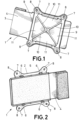
- Figures 1 and 2 show an exemplary implementation of a support bracket assembly (1) according to the invention, that comprises a support bracket (2) made of a plastic material, and a printed circuit board (3) conventionally comprising a board (4) and electronic components (5) and optionally a connector (19) fitted to the board (4), conventionally welded to connection tracks of the PCB.
- the support bracket (2) and a printed circuit board (3) are both complementary configured, such that they can be coupled together as shown in the figures.
- the assembly (1) includes coupling means (12) for mechanically coupling the support bracket (2) and the printed circuit board (3) together.
- these coupling means (12) are realized as clipping means (6) in the form of elastic tongues that retain the board (4) of the PCB at its edges by elastic pressure in a known manner.
- the board (4) of the PCB is shaped and dimensioned, so as to get coupled with the support bracket (2) by clipping or snap-fitting, by pressing the board (4) down against the clipping means (6).
- the support bracket (2) For attaching the assembly (1) to an external structure of an apparatus or vehicle (not shown) during the manufacturing process of the same, the support bracket (2) has two or more extension parts (7) located to overlap with fixation areas (not shown) of the apparatus on which the assembly is to be fixed. These extension parts (7) are integrally formed with the support bracket (2), and are arranged in the same, such that when the support bracket (2) and the PCB (3) are coupled together, in a plan view of the assembly (1), at least one extension part (7) protrudes outside the perimeter of the board (4) of the PCB (3) as shown in the Figures.
- the attaching means of the support bracket (2) are provided in those extension parts (7), and this implementation of the invention consist of passing-through holes (8), that would allow attaching the assembly (1) to an external structure by means of screws.
- these extension parts (7) are shaped and positioned depending on each practical application, so that the same PCB can be installed in different vehicle models simply by shaping the support bracket accordingly.
- the support bracket (2) is generally a planar body having a four-sided frame (9). Inside the area defined by the frame (9), there are apertures, in this example four triangular apertures (11) defined by crossbars (10).
- the support bracket (2) has four extension parts (7) at the corners of the frame (9), such that these extension parts (7) protrude outside the edges of the frame (9).
- the board (4) of the PCB can be fabricated with a rectangular configuration, which is very convenient to optimize the use of a mother board plank from which individual boards are cut-off.
- the PCB (4) is rectangular and the support bracket (2) is squared, and one side of the support bracket (2) (including the extension parts (7)), is longer than first sides of the board (4) of the PCB, and the other side of the support bracket (2) is shorter than at least one second side of the board (4) of the PCB (3).
- the length of one side of the frame (9), is similar to the length of the sort side of the board (4) of the PCB (3), in a way that the board (4) can be retained by the clipping means (6) at opposite sides.
- the support bracket (2) preferably has at least one aperture (11,11').
- the board (4) of the printed circuit board has at least one passing-through opening (13) overlapped with one aperture (11'), for allowing ventilation from one side of the assembly (1) to the other side.
- the support bracket (2) has at least one aperture (11) which does not overlap with an opening of the printed circuit board, that is, it is covered by the PCB.
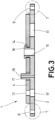
- the board (4) of the printed circuit board has at least one opening (14), and the support bracket (2) has one wall (15) inserted at least in part in that opening (14) for attaching the board (4) firmly to the support bracket (2).
- the wall (15) is a cylindrical tube, and it has a lib (16) configured to retain the board (4) attached to the support bracket (2) as shown in Figure 3 .
- the wall (15) configured as a cylindrical tube extends orthogonally with respect to the support bracket (2), and it also serves for ventilation as previously explained.
- the support bracket (2) has extension parts (7) which are parts that extend beyond the edges of perimeter of the board (4), such that the support bracket (2) and the board (4) do not overlap at these extension parts (7).
- the attaching means (8) of the support bracket (2), in this embodiment are passing-through holes provided in the extension parts (7).
- the support bracket (2) has a chimney (17) passing-through the board (4), in a way that the channel (18) of the chimney (17), communicates both sides of the assembly (1) for allowing air passing from one side of the assembly to the other side.
- This chimney (17) dimensioned to generate a chimney effect in a known manner, further enhance ventilation through the assembly due to the chimney effect.
- the length of chimney is larger than the height of the components fitted to the PCB, when attached to the support bracket, that is, the outlet of the chimney is above the components fitted to the PCB.
- This configuration of the chimney prevents that heat passing from one side of the PCB to the other side, would affect the PCB components.
Landscapes
- Engineering & Computer Science (AREA)
- Microelectronics & Electronic Packaging (AREA)
- Mounting Of Printed Circuit Boards And The Like (AREA)
Claims (14)
- Stützklammeranordnung (1) für Leiterplatten, umfassend:eine dedizierte Stützklammer (2) aufweisend Befestigungsmittel (8), welche dazu ausgebildet sind, die Befestigung der Stützklammer (2) an einer äußeren Struktur zu erlauben,eine Leiterplatte (3),wobei die Stützklammer (2) und die Leiterplatte (3) so ausgebildet sind, dass sie miteinander gekoppelt werden können, undKopplungsmittel (12) zur mechanischen Kopplung der Stützklammer (2) und der Leiterplatte (3) miteinander, sodass die Leiterplatte (3) von der Stützklammer (2) gestützt und gehalten wird,dadurch gekennzeichnet, dass sich Teile eines Bereichs der Leiterplatte (3) und der Stützklammer (2) überlappen und in direktem Kontakt sind, undwobei die Stützklammer (2) so ausgebildet ist, dass, wenn die Stützklammer (2) und die Leiterplatte (3) miteinander gekoppelt sind, in einer Draufsicht der Anordnung, mindestens ein Erstreckungsteil (7) der Stützklammer (2) außerhalb des Umfangs einer Platte (4) der Leiterplatte (3) hervorsteht, und wobei die Befestigungsmittel (8) der Stützklammer (2) in diesem Erstreckungsteil (7) vorgesehen sind.
- Stützklammeranordnung (1) nach Anspruch 1, wobei ein Teil der Stützklammer (2) geformt und dimensioniert ist, um mit einem Teil der Leiterplatte (3) übereinzustimmen, sodass die Leiterplatte (3) in der Stützklammer (2) aufgenommen ist und sich mit der Stützklammer (2) überlappt.
- Stützklammeranordnung (1) nach einem der vorhergehenden Ansprüche, wobei die Befestigungsmittel (8) Durchgangslöcher sind, um die Stützklammer (2) an der äußeren Struktur mittels Schrauben zu befestigen.
- Stützklammeranordnung (1) nach einem der vorhergehenden Ansprüche, wobei die Kopplungsmittel (12) Klemmmittel (6) und/oder Schrauben umfassen.
- Stützklammeranordnung (1) nach einem der vorhergehenden Ansprüche, wobei die Stützklammer (2) aus einem elektrisch isolierenden Material hergestellt ist.
- Stützklammeranordnung (1) nach einem der vorhergehenden Ansprüche, wobei mindestens ein Teil der Stützklammer (2) aus metallischem Material hergestellt ist, und wobei die Leiterplatte (3) eine Wärmesenke aufweist, welche dazu angeordnet ist, in Kontakt mit dem metallischen Teil der Stützklammer (2) zu sein, sodass Wärme von der Wärmesenke auf den metallischen Teil der Stützklammer (2) übertragen werden kann, um die Wärmeabfuhr zu erhöhen.
- Stützklammeranordnung (1) nach einem der vorhergehenden Ansprüche, wobei die Stützklammer (2) mindestens eine Öffnung (11') aufweist und wobei die Platte (4) der Leiterplatte eine Durchgangsbohrung (13) aufweist, welche sich mit dieser Öffnung (11') überlappt, um die Belüftung von einer Seite der Anordnung (1) zur anderen Seite zu erlauben.
- Stützklammeranordnung (1) nach einem der vorhergehenden Ansprüche, wobei die Platte (4) der Leiterplatte mindestens eine Bohrung (14) aufweist, und die Stützklammer (2) eine Wand (15) aufweist, welche mindestens teilweise in diese Bohrung (14) eingeführt ist, um die Platte (4) fest an der Stützklammer (2) zu befestigen.
- Stützklammeranordnung (1) nach Anspruch 8, wobei die Wand (15) ein Rohr ist, welches sich orthogonal in Bezug auf die Stützklammer (2) erstreckt.
- Stützklammeranordnung (1) nach einem der vorhergehenden Ansprüche, wobei die Stützklammer (2) einen Rahmen (9) aufweist, welcher mindestens eine Öffnung (11) in einem innerhalb des Rahmens definierten Bereich aufweist.
- Stützklammeranordnung (1) nach Anspruch 10, wobei der Rahmen (9) mindestens einen Erstreckungsteil (7) aufweist, welcher außerhalb des Rahmens (9) hervorsteht.
- Stützklammeranordnung (1) nach einem der vorhergehenden Ansprüche, aufweisend mindestens eine Öffnung (11) zur Verringerung deren Gewichts, und wobei das Gesamtvolumen einer oder mehrerer dieser Öffnungen mindestens 50 % des Gesamtvolumens der Stützklammer ist, und wobei eine oder mehrere dieser Öffnungen von der Leiterplatte gedeckt sind.
- Stützklammeranordnung (1) nach einem der Ansprüche 10-12, wobei der Rahmen (9) der Stützklammer (2) eine rechteckige oder quadratische Ausbildung aufweist.
- Stützklammeranordnung (1) nach einem der vorhergehenden Ansprüche, wobei die Stützklammer (2) einen Kamin (17) aufweist, welcher derart durch die Platte (4) durchgeht, dass der Kamin (17) beide Seiten der Anordnung (1) kommuniziert, um zu erlauben, dass Luft von einer Seite der Anordnung zur anderen Seite durchgeht.
Priority Applications (1)
| Application Number | Priority Date | Filing Date | Title |
|---|---|---|---|
| EP21382191.1A EP4057787B1 (de) | 2021-03-08 | 2021-03-08 | Stützklammeranordnung für leiterplatten |
Applications Claiming Priority (1)
| Application Number | Priority Date | Filing Date | Title |
|---|---|---|---|
| EP21382191.1A EP4057787B1 (de) | 2021-03-08 | 2021-03-08 | Stützklammeranordnung für leiterplatten |
Publications (2)
| Publication Number | Publication Date |
|---|---|
| EP4057787A1 EP4057787A1 (de) | 2022-09-14 |
| EP4057787B1 true EP4057787B1 (de) | 2024-10-09 |
Family
ID=75223261
Family Applications (1)
| Application Number | Title | Priority Date | Filing Date |
|---|---|---|---|
| EP21382191.1A Active EP4057787B1 (de) | 2021-03-08 | 2021-03-08 | Stützklammeranordnung für leiterplatten |
Country Status (1)
| Country | Link |
|---|---|
| EP (1) | EP4057787B1 (de) |
Family Cites Families (1)
| Publication number | Priority date | Publication date | Assignee | Title |
|---|---|---|---|---|
| US7616126B2 (en) * | 2006-07-18 | 2009-11-10 | Gentex Corporation | Optical particle detectors |
-
2021
- 2021-03-08 EP EP21382191.1A patent/EP4057787B1/de active Active
Also Published As
| Publication number | Publication date |
|---|---|
| EP4057787A1 (de) | 2022-09-14 |
Similar Documents
| Publication | Publication Date | Title |
|---|---|---|
| EP2633232B1 (de) | Beleuchtungsanordnung | |
| EP2807908B1 (de) | Vorrichtung, insbesondere schaltschrank, mit gehäuse | |
| US8383940B2 (en) | Bus bar attaching member and room lamp for vehicle having bus bar attaching member | |
| CN110062719B (zh) | 多媒体控制单元的散热装置 | |
| EP4057787B1 (de) | Stützklammeranordnung für leiterplatten | |
| CN206771149U (zh) | 照明器具 | |
| KR101487931B1 (ko) | 조명용 광센서 패키지 | |
| CN210807563U (zh) | 一种硅麦克风 | |
| KR100317096B1 (ko) | 전기장치 | |
| JP2015220093A (ja) | 照明器具 | |
| KR102425986B1 (ko) | 차폐부를 구비한 전기 시스템 | |
| CN220173471U (zh) | 一种pcb板的绝缘隔离结构及变频器 | |
| WO2008047815A1 (en) | Airconditioner with outdoor unit with insect proof closed spacer between printed wiring board and electric module | |
| CN210801081U (zh) | 细长型微波感应器 | |
| WO2022168569A1 (ja) | 電気装置 | |
| CN210118936U (zh) | 电控组件、用于电控组件的固定板及具有其的空调器 | |
| US20220320792A1 (en) | Electric apparatus | |
| JP4671119B2 (ja) | 安定器及び照明装置 | |
| EP4600687A1 (de) | Radarvorrichtung und verfahren zur herstellung davon | |
| CN218831701U (zh) | 一种激光除虫装置 | |
| JP2006235626A (ja) | シャーシベース組立体と、それを適用したプラズマ表示装置の組立体 | |
| CN217216522U (zh) | 一种晶体滤波器、电连接结构及电子设备 | |
| CN215529663U (zh) | 柜体散热装置及智能柜 | |
| JP2000252680A (ja) | 受光ユニット | |
| JP5704042B2 (ja) | 電子制御装置 |
Legal Events
| Date | Code | Title | Description |
|---|---|---|---|
| PUAI | Public reference made under article 153(3) epc to a published international application that has entered the european phase |
Free format text: ORIGINAL CODE: 0009012 |
|
| STAA | Information on the status of an ep patent application or granted ep patent |
Free format text: STATUS: THE APPLICATION HAS BEEN PUBLISHED |
|
| AK | Designated contracting states |
Kind code of ref document: A1 Designated state(s): AL AT BE BG CH CY CZ DE DK EE ES FI FR GB GR HR HU IE IS IT LI LT LU LV MC MK MT NL NO PL PT RO RS SE SI SK SM TR |
|
| STAA | Information on the status of an ep patent application or granted ep patent |
Free format text: STATUS: REQUEST FOR EXAMINATION WAS MADE |
|
| 17P | Request for examination filed |
Effective date: 20230314 |
|
| RBV | Designated contracting states (corrected) |
Designated state(s): AL AT BE BG CH CY CZ DE DK EE ES FI FR GB GR HR HU IE IS IT LI LT LU LV MC MK MT NL NO PL PT RO RS SE SI SK SM TR |
|
| GRAP | Despatch of communication of intention to grant a patent |
Free format text: ORIGINAL CODE: EPIDOSNIGR1 |
|
| STAA | Information on the status of an ep patent application or granted ep patent |
Free format text: STATUS: GRANT OF PATENT IS INTENDED |
|
| INTG | Intention to grant announced |
Effective date: 20240508 |
|
| GRAS | Grant fee paid |
Free format text: ORIGINAL CODE: EPIDOSNIGR3 |
|
| GRAA | (expected) grant |
Free format text: ORIGINAL CODE: 0009210 |
|
| STAA | Information on the status of an ep patent application or granted ep patent |
Free format text: STATUS: THE PATENT HAS BEEN GRANTED |
|
| AK | Designated contracting states |
Kind code of ref document: B1 Designated state(s): AL AT BE BG CH CY CZ DE DK EE ES FI FR GB GR HR HU IE IS IT LI LT LU LV MC MK MT NL NO PL PT RO RS SE SI SK SM TR |
|
| REG | Reference to a national code |
Ref country code: CH Ref legal event code: EP |
|
| REG | Reference to a national code |
Ref country code: DE Ref legal event code: R096 Ref document number: 602021019910 Country of ref document: DE |
|
| REG | Reference to a national code |
Ref country code: IE Ref legal event code: FG4D |
|
| REG | Reference to a national code |
Ref country code: LT Ref legal event code: MG9D |
|
| REG | Reference to a national code |
Ref country code: NL Ref legal event code: MP Effective date: 20241009 |
|
| REG | Reference to a national code |
Ref country code: AT Ref legal event code: MK05 Ref document number: 1732077 Country of ref document: AT Kind code of ref document: T Effective date: 20241009 |
|
| PG25 | Lapsed in a contracting state [announced via postgrant information from national office to epo] |
Ref country code: NL Free format text: LAPSE BECAUSE OF FAILURE TO SUBMIT A TRANSLATION OF THE DESCRIPTION OR TO PAY THE FEE WITHIN THE PRESCRIBED TIME-LIMIT Effective date: 20241009 |
|
| PG25 | Lapsed in a contracting state [announced via postgrant information from national office to epo] |
Ref country code: NL Free format text: LAPSE BECAUSE OF FAILURE TO SUBMIT A TRANSLATION OF THE DESCRIPTION OR TO PAY THE FEE WITHIN THE PRESCRIBED TIME-LIMIT Effective date: 20241009 |
|
| PG25 | Lapsed in a contracting state [announced via postgrant information from national office to epo] |
Ref country code: IS Free format text: LAPSE BECAUSE OF FAILURE TO SUBMIT A TRANSLATION OF THE DESCRIPTION OR TO PAY THE FEE WITHIN THE PRESCRIBED TIME-LIMIT Effective date: 20250209 Ref country code: HR Free format text: LAPSE BECAUSE OF FAILURE TO SUBMIT A TRANSLATION OF THE DESCRIPTION OR TO PAY THE FEE WITHIN THE PRESCRIBED TIME-LIMIT Effective date: 20241009 Ref country code: PT Free format text: LAPSE BECAUSE OF FAILURE TO SUBMIT A TRANSLATION OF THE DESCRIPTION OR TO PAY THE FEE WITHIN THE PRESCRIBED TIME-LIMIT Effective date: 20250210 |
|
| PG25 | Lapsed in a contracting state [announced via postgrant information from national office to epo] |
Ref country code: FI Free format text: LAPSE BECAUSE OF FAILURE TO SUBMIT A TRANSLATION OF THE DESCRIPTION OR TO PAY THE FEE WITHIN THE PRESCRIBED TIME-LIMIT Effective date: 20241009 |
|
| PG25 | Lapsed in a contracting state [announced via postgrant information from national office to epo] |
Ref country code: BG Free format text: LAPSE BECAUSE OF FAILURE TO SUBMIT A TRANSLATION OF THE DESCRIPTION OR TO PAY THE FEE WITHIN THE PRESCRIBED TIME-LIMIT Effective date: 20241009 |
|
| PG25 | Lapsed in a contracting state [announced via postgrant information from national office to epo] |
Ref country code: ES Free format text: LAPSE BECAUSE OF FAILURE TO SUBMIT A TRANSLATION OF THE DESCRIPTION OR TO PAY THE FEE WITHIN THE PRESCRIBED TIME-LIMIT Effective date: 20241009 |
|
| PG25 | Lapsed in a contracting state [announced via postgrant information from national office to epo] |
Ref country code: NO Free format text: LAPSE BECAUSE OF FAILURE TO SUBMIT A TRANSLATION OF THE DESCRIPTION OR TO PAY THE FEE WITHIN THE PRESCRIBED TIME-LIMIT Effective date: 20250109 |
|
| PG25 | Lapsed in a contracting state [announced via postgrant information from national office to epo] |
Ref country code: LV Free format text: LAPSE BECAUSE OF FAILURE TO SUBMIT A TRANSLATION OF THE DESCRIPTION OR TO PAY THE FEE WITHIN THE PRESCRIBED TIME-LIMIT Effective date: 20241009 Ref country code: AT Free format text: LAPSE BECAUSE OF FAILURE TO SUBMIT A TRANSLATION OF THE DESCRIPTION OR TO PAY THE FEE WITHIN THE PRESCRIBED TIME-LIMIT Effective date: 20241009 Ref country code: GR Free format text: LAPSE BECAUSE OF FAILURE TO SUBMIT A TRANSLATION OF THE DESCRIPTION OR TO PAY THE FEE WITHIN THE PRESCRIBED TIME-LIMIT Effective date: 20250110 |
|
| PG25 | Lapsed in a contracting state [announced via postgrant information from national office to epo] |
Ref country code: PL Free format text: LAPSE BECAUSE OF FAILURE TO SUBMIT A TRANSLATION OF THE DESCRIPTION OR TO PAY THE FEE WITHIN THE PRESCRIBED TIME-LIMIT Effective date: 20241009 |
|
| PG25 | Lapsed in a contracting state [announced via postgrant information from national office to epo] |
Ref country code: RS Free format text: LAPSE BECAUSE OF FAILURE TO SUBMIT A TRANSLATION OF THE DESCRIPTION OR TO PAY THE FEE WITHIN THE PRESCRIBED TIME-LIMIT Effective date: 20250109 |
|
| PG25 | Lapsed in a contracting state [announced via postgrant information from national office to epo] |
Ref country code: SM Free format text: LAPSE BECAUSE OF FAILURE TO SUBMIT A TRANSLATION OF THE DESCRIPTION OR TO PAY THE FEE WITHIN THE PRESCRIBED TIME-LIMIT Effective date: 20241009 |
|
| PGFP | Annual fee paid to national office [announced via postgrant information from national office to epo] |
Ref country code: DE Payment date: 20250528 Year of fee payment: 5 |
|
| PG25 | Lapsed in a contracting state [announced via postgrant information from national office to epo] |
Ref country code: DK Free format text: LAPSE BECAUSE OF FAILURE TO SUBMIT A TRANSLATION OF THE DESCRIPTION OR TO PAY THE FEE WITHIN THE PRESCRIBED TIME-LIMIT Effective date: 20241009 |
|
| REG | Reference to a national code |
Ref country code: DE Ref legal event code: R097 Ref document number: 602021019910 Country of ref document: DE |
|
| PG25 | Lapsed in a contracting state [announced via postgrant information from national office to epo] |
Ref country code: EE Free format text: LAPSE BECAUSE OF FAILURE TO SUBMIT A TRANSLATION OF THE DESCRIPTION OR TO PAY THE FEE WITHIN THE PRESCRIBED TIME-LIMIT Effective date: 20241009 |
|
| PG25 | Lapsed in a contracting state [announced via postgrant information from national office to epo] |
Ref country code: RO Free format text: LAPSE BECAUSE OF FAILURE TO SUBMIT A TRANSLATION OF THE DESCRIPTION OR TO PAY THE FEE WITHIN THE PRESCRIBED TIME-LIMIT Effective date: 20241009 |
|
| PG25 | Lapsed in a contracting state [announced via postgrant information from national office to epo] |
Ref country code: SK Free format text: LAPSE BECAUSE OF FAILURE TO SUBMIT A TRANSLATION OF THE DESCRIPTION OR TO PAY THE FEE WITHIN THE PRESCRIBED TIME-LIMIT Effective date: 20241009 |
|
| PG25 | Lapsed in a contracting state [announced via postgrant information from national office to epo] |
Ref country code: CZ Free format text: LAPSE BECAUSE OF FAILURE TO SUBMIT A TRANSLATION OF THE DESCRIPTION OR TO PAY THE FEE WITHIN THE PRESCRIBED TIME-LIMIT Effective date: 20241009 |
|
| PG25 | Lapsed in a contracting state [announced via postgrant information from national office to epo] |
Ref country code: IT Free format text: LAPSE BECAUSE OF FAILURE TO SUBMIT A TRANSLATION OF THE DESCRIPTION OR TO PAY THE FEE WITHIN THE PRESCRIBED TIME-LIMIT Effective date: 20241009 |
|
| PLBE | No opposition filed within time limit |
Free format text: ORIGINAL CODE: 0009261 |
|
| STAA | Information on the status of an ep patent application or granted ep patent |
Free format text: STATUS: NO OPPOSITION FILED WITHIN TIME LIMIT |
|
| PG25 | Lapsed in a contracting state [announced via postgrant information from national office to epo] |
Ref country code: SE Free format text: LAPSE BECAUSE OF FAILURE TO SUBMIT A TRANSLATION OF THE DESCRIPTION OR TO PAY THE FEE WITHIN THE PRESCRIBED TIME-LIMIT Effective date: 20241009 |
|
| 26N | No opposition filed |
Effective date: 20250710 |
|
| PG25 | Lapsed in a contracting state [announced via postgrant information from national office to epo] |
Ref country code: MC Free format text: LAPSE BECAUSE OF FAILURE TO SUBMIT A TRANSLATION OF THE DESCRIPTION OR TO PAY THE FEE WITHIN THE PRESCRIBED TIME-LIMIT Effective date: 20241009 |
|
| REG | Reference to a national code |
Ref country code: CH Ref legal event code: H13 Free format text: ST27 STATUS EVENT CODE: U-0-0-H10-H13 (AS PROVIDED BY THE NATIONAL OFFICE) Effective date: 20251023 |
|
| PG25 | Lapsed in a contracting state [announced via postgrant information from national office to epo] |
Ref country code: LU Free format text: LAPSE BECAUSE OF NON-PAYMENT OF DUE FEES Effective date: 20250308 |
|
| GBPC | Gb: european patent ceased through non-payment of renewal fee |
Effective date: 20250308 |