EP4057784A1 - Multilayer wiring board - Google Patents
Multilayer wiring board Download PDFInfo
- Publication number
- EP4057784A1 EP4057784A1 EP20884642.8A EP20884642A EP4057784A1 EP 4057784 A1 EP4057784 A1 EP 4057784A1 EP 20884642 A EP20884642 A EP 20884642A EP 4057784 A1 EP4057784 A1 EP 4057784A1
- Authority
- EP
- European Patent Office
- Prior art keywords
- wiring substrate
- layer
- joining
- layers
- joining layer
- Prior art date
- Legal status (The legal status is an assumption and is not a legal conclusion. Google has not performed a legal analysis and makes no representation as to the accuracy of the status listed.)
- Pending
Links
Images




Classifications
-
- H—ELECTRICITY
- H05—ELECTRIC TECHNIQUES NOT OTHERWISE PROVIDED FOR
- H05K—PRINTED CIRCUITS; CASINGS OR CONSTRUCTIONAL DETAILS OF ELECTRIC APPARATUS; MANUFACTURE OF ASSEMBLAGES OF ELECTRICAL COMPONENTS
- H05K3/00—Apparatus or processes for manufacturing printed circuits
- H05K3/46—Manufacturing multilayer circuits
- H05K3/4611—Manufacturing multilayer circuits by laminating two or more circuit boards
- H05K3/4626—Manufacturing multilayer circuits by laminating two or more circuit boards characterised by the insulating layers or materials
- H05K3/4632—Manufacturing multilayer circuits by laminating two or more circuit boards characterised by the insulating layers or materials laminating thermoplastic or uncured resin sheets comprising printed circuits without added adhesive materials between the sheets
-
- H—ELECTRICITY
- H10—SEMICONDUCTOR DEVICES; ELECTRIC SOLID-STATE DEVICES NOT OTHERWISE PROVIDED FOR
- H10W—GENERIC PACKAGES, INTERCONNECTIONS, CONNECTORS OR OTHER CONSTRUCTIONAL DETAILS OF DEVICES COVERED BY CLASS H10
- H10W70/00—Package substrates; Interposers; Redistribution layers [RDL]
- H10W70/60—Insulating or insulated package substrates; Interposers; Redistribution layers
- H10W70/67—Insulating or insulated package substrates; Interposers; Redistribution layers characterised by their insulating layers or insulating parts
- H10W70/69—Insulating materials thereof
- H10W70/695—Organic materials
-
- G—PHYSICS
- G01—MEASURING; TESTING
- G01R—MEASURING ELECTRIC VARIABLES; MEASURING MAGNETIC VARIABLES
- G01R1/00—Details of instruments or arrangements of the types included in groups G01R5/00 - G01R13/00 and G01R31/00
- G01R1/02—General constructional details
- G01R1/04—Housings; Supporting members; Arrangements of terminals
- G01R1/0408—Test fixtures or contact fields; Connectors or connecting adaptors; Test clips; Test sockets
-
- H—ELECTRICITY
- H05—ELECTRIC TECHNIQUES NOT OTHERWISE PROVIDED FOR
- H05K—PRINTED CIRCUITS; CASINGS OR CONSTRUCTIONAL DETAILS OF ELECTRIC APPARATUS; MANUFACTURE OF ASSEMBLAGES OF ELECTRICAL COMPONENTS
- H05K1/00—Printed circuits
- H05K1/02—Details
- H05K1/0296—Conductive pattern lay-out details not covered by sub groups H05K1/02 - H05K1/0295
- H05K1/0298—Multilayer circuits
-
- H—ELECTRICITY
- H05—ELECTRIC TECHNIQUES NOT OTHERWISE PROVIDED FOR
- H05K—PRINTED CIRCUITS; CASINGS OR CONSTRUCTIONAL DETAILS OF ELECTRIC APPARATUS; MANUFACTURE OF ASSEMBLAGES OF ELECTRICAL COMPONENTS
- H05K1/00—Printed circuits
- H05K1/02—Details
- H05K1/03—Use of materials for the substrate
- H05K1/0306—Inorganic insulating substrates, e.g. ceramic, glass
-
- H—ELECTRICITY
- H05—ELECTRIC TECHNIQUES NOT OTHERWISE PROVIDED FOR
- H05K—PRINTED CIRCUITS; CASINGS OR CONSTRUCTIONAL DETAILS OF ELECTRIC APPARATUS; MANUFACTURE OF ASSEMBLAGES OF ELECTRICAL COMPONENTS
- H05K1/00—Printed circuits
- H05K1/02—Details
- H05K1/14—Structural association of two or more printed circuits
- H05K1/144—Stacked arrangements of planar printed circuit boards
-
- H—ELECTRICITY
- H05—ELECTRIC TECHNIQUES NOT OTHERWISE PROVIDED FOR
- H05K—PRINTED CIRCUITS; CASINGS OR CONSTRUCTIONAL DETAILS OF ELECTRIC APPARATUS; MANUFACTURE OF ASSEMBLAGES OF ELECTRICAL COMPONENTS
- H05K3/00—Apparatus or processes for manufacturing printed circuits
- H05K3/46—Manufacturing multilayer circuits
- H05K3/4611—Manufacturing multilayer circuits by laminating two or more circuit boards
- H05K3/4614—Manufacturing multilayer circuits by laminating two or more circuit boards the electrical connections between the circuit boards being made during lamination
- H05K3/462—Manufacturing multilayer circuits by laminating two or more circuit boards the electrical connections between the circuit boards being made during lamination characterized by laminating only or mainly similar double-sided circuit boards
-
- H—ELECTRICITY
- H05—ELECTRIC TECHNIQUES NOT OTHERWISE PROVIDED FOR
- H05K—PRINTED CIRCUITS; CASINGS OR CONSTRUCTIONAL DETAILS OF ELECTRIC APPARATUS; MANUFACTURE OF ASSEMBLAGES OF ELECTRICAL COMPONENTS
- H05K3/00—Apparatus or processes for manufacturing printed circuits
- H05K3/46—Manufacturing multilayer circuits
- H05K3/4611—Manufacturing multilayer circuits by laminating two or more circuit boards
- H05K3/4626—Manufacturing multilayer circuits by laminating two or more circuit boards characterised by the insulating layers or materials
- H05K3/4629—Manufacturing multilayer circuits by laminating two or more circuit boards characterised by the insulating layers or materials laminating inorganic sheets comprising printed circuits, e.g. green ceramic sheets
-
- H—ELECTRICITY
- H05—ELECTRIC TECHNIQUES NOT OTHERWISE PROVIDED FOR
- H05K—PRINTED CIRCUITS; CASINGS OR CONSTRUCTIONAL DETAILS OF ELECTRIC APPARATUS; MANUFACTURE OF ASSEMBLAGES OF ELECTRICAL COMPONENTS
- H05K3/00—Apparatus or processes for manufacturing printed circuits
- H05K3/46—Manufacturing multilayer circuits
- H05K3/4688—Composite multilayer circuits, i.e. comprising insulating layers having different properties
-
- H—ELECTRICITY
- H10—SEMICONDUCTOR DEVICES; ELECTRIC SOLID-STATE DEVICES NOT OTHERWISE PROVIDED FOR
- H10W—GENERIC PACKAGES, INTERCONNECTIONS, CONNECTORS OR OTHER CONSTRUCTIONAL DETAILS OF DEVICES COVERED BY CLASS H10
- H10W70/00—Package substrates; Interposers; Redistribution layers [RDL]
- H10W70/01—Manufacture or treatment
- H10W70/05—Manufacture or treatment of insulating or insulated package substrates, or of interposers, or of redistribution layers
-
- H—ELECTRICITY
- H10—SEMICONDUCTOR DEVICES; ELECTRIC SOLID-STATE DEVICES NOT OTHERWISE PROVIDED FOR
- H10W—GENERIC PACKAGES, INTERCONNECTIONS, CONNECTORS OR OTHER CONSTRUCTIONAL DETAILS OF DEVICES COVERED BY CLASS H10
- H10W70/00—Package substrates; Interposers; Redistribution layers [RDL]
- H10W70/60—Insulating or insulated package substrates; Interposers; Redistribution layers
- H10W70/67—Insulating or insulated package substrates; Interposers; Redistribution layers characterised by their insulating layers or insulating parts
- H10W70/68—Shapes or dispositions thereof
- H10W70/685—Shapes or dispositions thereof comprising multiple insulating layers
-
- H—ELECTRICITY
- H10—SEMICONDUCTOR DEVICES; ELECTRIC SOLID-STATE DEVICES NOT OTHERWISE PROVIDED FOR
- H10W—GENERIC PACKAGES, INTERCONNECTIONS, CONNECTORS OR OTHER CONSTRUCTIONAL DETAILS OF DEVICES COVERED BY CLASS H10
- H10W70/00—Package substrates; Interposers; Redistribution layers [RDL]
- H10W70/60—Insulating or insulated package substrates; Interposers; Redistribution layers
- H10W70/67—Insulating or insulated package substrates; Interposers; Redistribution layers characterised by their insulating layers or insulating parts
- H10W70/68—Shapes or dispositions thereof
- H10W70/685—Shapes or dispositions thereof comprising multiple insulating layers
- H10W70/686—Shapes or dispositions thereof comprising multiple insulating layers the multiple insulating layers having different compositions, e.g. polymer layer on glass substrate
-
- G—PHYSICS
- G01—MEASURING; TESTING
- G01R—MEASURING ELECTRIC VARIABLES; MEASURING MAGNETIC VARIABLES
- G01R1/00—Details of instruments or arrangements of the types included in groups G01R5/00 - G01R13/00 and G01R31/00
- G01R1/02—General constructional details
- G01R1/06—Measuring leads; Measuring probes
- G01R1/067—Measuring probes
- G01R1/073—Multiple probes
- G01R1/07307—Multiple probes with individual probe elements, e.g. needles, cantilever beams or bump contacts, fixed in relation to each other, e.g. bed of nails fixture or probe card
-
- G—PHYSICS
- G01—MEASURING; TESTING
- G01R—MEASURING ELECTRIC VARIABLES; MEASURING MAGNETIC VARIABLES
- G01R1/00—Details of instruments or arrangements of the types included in groups G01R5/00 - G01R13/00 and G01R31/00
- G01R1/02—General constructional details
- G01R1/06—Measuring leads; Measuring probes
- G01R1/067—Measuring probes
- G01R1/073—Multiple probes
- G01R1/07307—Multiple probes with individual probe elements, e.g. needles, cantilever beams or bump contacts, fixed in relation to each other, e.g. bed of nails fixture or probe card
- G01R1/07364—Multiple probes with individual probe elements, e.g. needles, cantilever beams or bump contacts, fixed in relation to each other, e.g. bed of nails fixture or probe card with provisions for altering position, number or connection of probe tips; Adapting to differences in pitch
- G01R1/07378—Multiple probes with individual probe elements, e.g. needles, cantilever beams or bump contacts, fixed in relation to each other, e.g. bed of nails fixture or probe card with provisions for altering position, number or connection of probe tips; Adapting to differences in pitch using an intermediate adapter, e.g. space transformers
-
- H—ELECTRICITY
- H05—ELECTRIC TECHNIQUES NOT OTHERWISE PROVIDED FOR
- H05K—PRINTED CIRCUITS; CASINGS OR CONSTRUCTIONAL DETAILS OF ELECTRIC APPARATUS; MANUFACTURE OF ASSEMBLAGES OF ELECTRICAL COMPONENTS
- H05K2201/00—Indexing scheme relating to printed circuits covered by H05K1/00
- H05K2201/09—Shape and layout
- H05K2201/09209—Shape and layout details of conductors
- H05K2201/095—Conductive through-holes or vias
- H05K2201/096—Vertically aligned vias, holes or stacked vias
-
- H—ELECTRICITY
- H05—ELECTRIC TECHNIQUES NOT OTHERWISE PROVIDED FOR
- H05K—PRINTED CIRCUITS; CASINGS OR CONSTRUCTIONAL DETAILS OF ELECTRIC APPARATUS; MANUFACTURE OF ASSEMBLAGES OF ELECTRICAL COMPONENTS
- H05K2203/00—Indexing scheme relating to apparatus or processes for manufacturing printed circuits covered by H05K3/00
- H05K2203/06—Lamination
- H05K2203/061—Lamination of previously made multilayered subassemblies
-
- H—ELECTRICITY
- H05—ELECTRIC TECHNIQUES NOT OTHERWISE PROVIDED FOR
- H05K—PRINTED CIRCUITS; CASINGS OR CONSTRUCTIONAL DETAILS OF ELECTRIC APPARATUS; MANUFACTURE OF ASSEMBLAGES OF ELECTRICAL COMPONENTS
- H05K3/00—Apparatus or processes for manufacturing printed circuits
- H05K3/46—Manufacturing multilayer circuits
- H05K3/4611—Manufacturing multilayer circuits by laminating two or more circuit boards
- H05K3/4614—Manufacturing multilayer circuits by laminating two or more circuit boards the electrical connections between the circuit boards being made during lamination
Definitions
- the present invention relates to a multilayer wiring substrate.
- a wiring substrate described in PTL 2 includes a joining layer that joins a front surface of a ceramic substrate and a back surface of a wiring layer to each other.
- the joining layer has a core layer made of a thermosetting resin and an adhesive layer made of a thermosetting resin having a lower elasticity than that of the core layer.
- the number of man-hours for manufacturing a ceramic that is used for a multilayer wiring substrate is larger than the number of man-hours for manufacturing other components.
- the number of man-hours for manufacturing the entire multilayer wiring substrate may increase, and the time required for manufacturing the multilayer wiring substrate may increase.
- PTL 1 and PTL 2 disclose a method of manufacturing each layer in the multilayer wiring substrate; however, PTL 1 and PTL 2 do not consider the numbers of man-hours for manufacturing the multilayer wiring substrate and the ceramic.
- To decrease the number of man-hours for manufacturing the multilayer wiring substrate there has been a demand of reusing the ceramic that takes many man-hours for manufacturing.
- the present invention is made to solve the above-described problem and an object of the invention is to provide a ceramic substrate that is used for a multilayer wiring substrate and that is reusable.
- the present invention is made to solve the above-described problem, and can be implemented as aspects as follows.
- the thickness of each layer of the first wiring substrate in the stacking direction is smaller than the thickness of the joining layer. Namely, with the configuration, the thickness of the first wiring substrate can be decreased. Thus, the number of wiring layers that constitute the first wiring substrate can be increased, and the wires of a circuit that is constituted by the wiring layers can be thinned.
- the present invention can be implemented according to various aspects.
- the present invention can be implemented according to aspects including a wiring substrate, a multilayer wiring substrate, a semiconductor wiring substrate, a component including any one of the substrates, and a method of manufacturing the wiring substrate or the multilayer wiring substrate.
- Fig. 1 is a schematic cross-sectional view of a multilayer wiring substrate 100 as an embodiment of the present invention.
- the multilayer wiring substrate 100 of the present embodiment is used as a probe card that is used for semiconductor inspection.
- the probe card is a tool for inspecting electric time characteristics of a plurality of electronic components formed on a silicon wafer.
- Fig. 1 illustrates an overview of a cross section in a stacking direction of respective layers that form the multilayer wiring substrate 100.
- the multilayer wiring substrate 100 includes a first wiring substrate 10 in which a plurality of resin layers made of a thermosetting resin are stacked, a second wiring substrate made of a ceramic, and a joining layer 30 disposed between a back surface of the first wiring substrate 10 and a front surface of the second wiring substrate 20.
- Fig. 1 omits illustration for the details of the first wiring substrate 10, and the details of the first wiring substrate 10 will be described also with reference to Fig. 2 .
- the second wiring substrate 20 is a substrate in which three ceramic layers C21 to C23 made of a ceramic are stacked.
- the three ceramic layers C21 to C23 are substrates made of aluminum oxide and having the same thickness.
- a connecting terminal 23 is formed on a front surface of the ceramic layer C21.
- Wiring layers 21 and 22 having predetermined patterns are formed on respective front surfaces of the ceramic layers C22 and C23.
- a connecting terminal 24 is formed on a back surface of the ceramic layer C23. Namely, the connecting terminals 23 and 24 are formed on the front surface and a back surface of the second wiring substrate 20.
- a via conductor V21 that electrically connects the connecting terminal 23 formed on the front surface of the ceramic layer C21 and the wiring layer 21 to each other is formed in the ceramic layer C21.
- a via conductor V22 that electrically connects the wiring layer 21 and the wiring layer 22 to each other is formed in the ceramic layer C22.
- a via conductor V23 that connects the wiring layer 22 and the connecting terminal 24 formed on the back surface of the ceramic layer C23 to each other is formed in the ceramic layer C23.
- Each of the via conductors V21 to V23 are made of W (tungsten).
- the via conductors V21 to V23 electrically connect the connecting terminal 23 formed on the front surface of the second wiring substrate 20 and the connecting terminal 24 formed on the back surface of the second wiring substrate 20 to each other.
- Fig. 2 is an explanatory diagram of a cross section of the wiring substrate 10.
- Fig. 2 presents a schematic diagram illustrating a cross section of the wiring substrate 10 in an enlarged manner only in the stacking direction.
- the first wiring substrate 10 of the present embodiment is a substrate in which a plurality of resin layers J11 to J13 made of a polyimide that is a thermosetting resin are stacked. Wiring layers 12 and 13 having predetermined patterns are formed between the resin layers J11 to J13 in a state in contact with the resin layers J11 to J13. Also, a connecting terminal 11 is formed on a front surface of the ceramic layer J11. A connecting terminal 14 is formed on a back surface of the ceramic layer J13.
- the connecting terminals 11 and 14 are formed on a front surface and the back surface of the first wiring substrate 10.
- the connecting terminal 11 is a terminal in which a Cu (copper) layer 11c, an Ni (nickel) layer 11n, and an Au (gold) layer 11a are stacked in that order from the front surface of the resin layer J11.
- the wiring layers 12 and 13, and the connecting terminal 14 are made of Cu-Ti.
- a via conductor V11 that electrically connects the connecting terminal 11 and the wiring layer 12 to each other is formed in the resin layer J11.
- a via conductor V12 that electrically connects the wiring layer 12 and the wiring layer 13 to each other is formed in the resin layer J12.
- a via conductor V13 that electrically connects the wiring layer 13 and the connecting terminal 14 to each other is formed in the resin layer J13.
- Each of the via conductors V11 to V13 is made of Cu-Ti.
- the via conductors V11 to V13 electrically connect the connecting terminal 11 formed on the front surface of the first wiring substrate 10 and the connecting terminal 14 formed on the back surface of the first wiring substrate 10 to each other.
- the first wiring substrate 10 of the present embodiment is manufactured by a buildup method of forming the wiring layer 13, the resin layer J12, the wiring layer 12, the resin layer J11, and the wiring layer 11 in that order on the resin layer J13, instead of being manufactured by preparing the resin layers J11 to J13 separately and then collectively stacking the resin layers J11 to J13.
- thicknesses t11 to t13 of the respective resin layers J11 to J13 of the present embodiment in the stacking direction are smaller than the thicknesses in the case where the resin layers J11 to J13 are separately prepared.
- Fig. 3 is a schematic cross-sectional view of the joining layer 30 before the first wiring substrate 10 and the second wiring substrate 20 are joined to each other.
- Fig. 3 presents a cross-sectional view illustrating a portion of the joining layer 30 in an enlarged manner.
- the joining layer 30 includes a base material 31 made of a polyimide that is a thermosetting resin, joining materials 32 and 33 disposed on both surfaces of the base material 31, and a conductive member 34.
- the joining materials 32 and 33 are made of a polyimide that is a thermoplastic resin and that is different from the polyimide of the base material 31.
- the polyimide of the thermoplastic resin and the polyimide of the thermosetting resin are distinguished from each other based on a glass transition point.
- a resin whose glass transition point is 300 degrees centigrade or higher is defined as a thermosetting resin
- a resin whose glass transition point is lower than 300 degrees centigrade is defined as a thermoplastic resin.
- the glass transition point can be specified by, for example, TMA method (Thermo Mechanical Analysis).
- the glass transition point of the polyimide of the thermoplastic resin is 240 degrees centigrade and the glass transition point of the polyimide of the thermosetting resin is 420 degrees centigrade.
- the base material 31 with a thickness t31 of 10 to 100 ⁇ m in the stacking direction is used.
- the thickness t31 is 30 ⁇ m.
- the joining materials 32 and 33 with thicknesses t32 and t33 of 15 ⁇ m or less in the stacking direction can be used.
- the thicknesses t32 and t33 are the same and are 3 ⁇ m.
- the thickness (t31 + t32 + t33) of the joining layer 30, which is the sum of the thicknesses of the base material 31 and the joining materials 32 and 33, is larger than the thickness of a layer (for example, J11) of the first wiring substrate 10.
- the thickness (for example, t11) of each layer of the first wiring substrate 10 in the stacking direction is smaller than the thickness of the joining layer 30.
- the conductive member 34 is made of Ag.
- the conductive member 34 is formed to penetrate through the joining layer 30 (the base material 31 and the joining materials 32 and 33). As illustrated in Fig. 3 , the conductive member 34 protrudes from a front surface and a back surface of the joining materials 32 and 33 in a thickness direction. As illustrated in Fig. 1 , the conductive member 34 formed in and on the joining layer 30 is formed at each position at which the conductive member 34 connects the connecting terminal 14 formed on the back surface of the first wiring substrate 10 and the connecting terminal 23 formed on the front surface of the second wiring substrate 20 to each other. Namely, the conductive member 34 electrically connects the connecting terminal 14 on the back surface of the first wiring substrate 10 and the connecting terminal 23 on the front surface of the second wiring substrate 20 to each other.
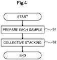
- Fig. 4 is a flowchart of a method of manufacturing the multilayer wiring substrate 100.
- the method of manufacturing the multilayer wiring substrate 100 first, the first wiring substrate 10, the second wiring substrate 20, and the joining layer 30 that are each a sample that constitutes the multilayer wiring substrate 100 are prepared (step S1). Then, in a state where the conductive member 34 of the joining layer 30 is disposed at the position at which the conductive member 34 connects the connecting terminal 14 of the first wiring substrate 10 and the connecting terminal 23 of the second wiring substrate 20 to each other, the first wiring substrate 10, the second wiring substrate 20, and the joining layer 30 are collectively stacked (step S2), thereby manufacturing the multilayer wiring substrate 100. Heat is applied to the joining layer 30 during the collective stacking.
- the joining materials 32 and 33 that are the thermoplastic resin of the joining layer 30 change to join the first wiring substrate 10 and the joining layer 30 to each other and to join the joining layer 30 and the second wiring substrate 20 to each other.
- the first wiring substrate 10 and the second wiring substrate 20 are joined to each other via the joining layer 30.
- Fig. 5 and Fig. 6 are explanatory diagrams of a method of manufacturing the joining layer 30.
- Fig. 5 presents a flowchart of the method of manufacturing the joining layer 30.
- Fig. 6 presents a portion of a cross section of the joining layer 30 that changes according to the flowchart, to meet the respective steps presented in Fig. 5 .
- a sheet of the joining layer 30 having the joining materials 32 and 33 formed on both the surfaces of the base material 31 is cut into a predetermined size (step S11).
- a frame is attached to the cut joining layer 30 (step S12).
- a through hole HL is formed by laser punching to extend through the joining layer 30 in the thickness direction (step S13).
- the formed through hole HL is filled with Ag that is to serve as the conductive member 34 (step S14), and the method of manufacturing the joining layer 30 is ended.
- the multilayer wiring substrate 100 of the present embodiment includes the joining layer 30 that is disposed between the back surface of the first wiring substrate 10 having the wiring layers 12 and 13 and the front surface of the second wiring substrate 20 made of the ceramic and that joins the first wiring substrate 10 and the second wiring substrate 20 to each other.
- a surface of the joining layer 30 adjacent to the second wiring substrate 20 is formed of the joining material 33 of the thermoplastic resin. Namely, the first wiring substrate 10 and the second wiring substrate 20 are joined to each other by the thermoplastic resin that makes the joining material 33.
- the thermoplastic resin changes, and the joining between the first wiring substrate 10 and the second wiring substrate 20 is released.
- the first wiring substrate 10 is formed of the plurality of layers made of the thermosetting resin, the joining between the respective layers is not released even when heat is applied.
- the completed multilayer wiring substrate 100 can be separated into the first wiring substrate 10 and the second wiring substrate 20, and the first wiring substrate 10 and the second wiring substrate 20 can be reused.
- reusing the second wiring substrate 20 that takes many man-hours for manufacturing can decrease the number of man-hours for manufacturing the multilayer wiring substrate 100.
- fabricating in advance a ceramic commonly usable for many multilayer wiring substrates 100 decreases the number of man-hours for manufacturing the multilayer wiring substrate 100.
- the joining layer 30 of the present embodiment includes the base material 31 made of the thermosetting resin, and the joining materials 32 and 33 of the thermoplastic resin disposed on both the surfaces of the base material 31.
- the joining layer 30 has the conductive member 34 formed to penetrate through the joining layer 30 in the stacking direction.
- the conductive member 34 electrically connects the connecting terminal 14 on the back surface of the first wiring substrate 10 and the connecting terminal 23 on the front surface of the second wiring substrate 20 to each other. Since the base material 31 is made of the thermosetting resin, the base material 31 is less likely to be deformed compared with the joining materials 32 and 33 made of the thermoplastic resin.
- the first wiring substrate 10 and the second wiring substrate 20 are joined to each other in a state where the joining can be released by the joining materials 32 and 33, and also are electrically stably connected to each other by the base material 31 that is less likely to be deformed.
- the thickness of a layer (for example, the resin layer J11) of the first wiring substrate 10 of the present embodiment in the stacking direction is smaller than the thickness of the joining layer 30. Hence, the thickness of the entire first wiring substrate 10 can be decreased. Thus, the number of wiring layers that constitute the first wiring substrate 10 can be increased, and wires of a circuit that is constituted by the wiring layers can be thinned.
- the present invention is not limited to the above-described embodiment, can be implemented in various embodiments within a range not departing from the gist of the invention, and can be modified, for example, as follows.
- the examples of the first wiring substrate 10, the second wiring substrate 20, and the joining layer 30 that constitute the multilayer wiring substrate 100 have been described.
- the respective configurations and respective shapes of the multilayer wiring substrate 100 can be modified in various ways.
- the first wiring substrate 10 of the above-described embodiment is the multilayer body of the three resin layers J11 to J13 as illustrated in Fig. 2
- the number of stacked layers may be two, or four or more.
- the thickness of each layer (for example, t11) in the stacking direction need not be smaller than the thickness of the joining layer 30.
- the layers may mixedly include a layer thinner than the joining layer 30 and a layer thicker than the joining layer 30.
- the resin layers J11 to J13 of the above-described embodiment are made of the polyimide of the thermosetting resin, the resin layers J11 to J13 may be made of another thermosetting resin.
- the predetermined patterns of the connecting terminals 11 and 14 and the wiring layers 12 and 13 can be modified. While the connecting terminal 11 formed on the front surface of the first wiring substrate 10 is the terminal in which the three metals of Au, Ni, and Cu are stacked, the connecting terminal 11 may be made of a kind of metal of the three metals, or may be made of another kind of metal (for example, Ag).
- the connecting terminal 14 can be omitted.
- the via conductor V13 in the resin layer J13 may be directly connected to the conductive member 34 that penetrates through the joining layer 30.
- the via conductors V11 to V13 that respectively penetrate through the resin layers J11 to J13 may be made of a conductive material other than Cu or Ti (titanium), and may be made of, for example, Ag.
- the second wiring substrate 20 of the above-described embodiment is the multilayer body of the three ceramic layers C21 to C23 made of the ceramic as illustrated in Fig. 1
- the second wiring substrate 20 may be a multilayer body including four or more layers, or, for example, may be formed of only one layer of the ceramic layer C21.
- the material that makes the ceramic layers C21 to C23 may be, for example, AlN (aluminum nitride), glass-ceramic, mullite, or BN, as a ceramic other than aluminum oxide.
- the layers may be made of ceramics different from one another. The thicknesses of the respective ceramic layers C21 to C23 in the stacking direction need not be the same and may differ from one another.
- the predetermined patterns of the wiring layers 21 and 23 and the connecting terminals 23 and 24 can be modified.
- the via conductors V21 to 23 that respectively penetrate through the ceramic layers C21 to C23 may be made of a conductive material other than W, for example, Mo (molybdenum), a mixed material of Mo and W, or Cu.
- the joining layer 30 of the above-described embodiment is the layer in which the base material 31 serves as a parent material and the joining materials 32 and 33 of the thermoplastic resin are formed on both the surfaces of the base material 31,
- the configuration of the joining layer 30 can be modified in various ways.
- only at least the joining material 33 on the back surface of the joining layer 30 adjacent to the second wiring substrate 20 may be made of a thermoplastic resin, and the joining material 32 on the front surface may be omitted.
- the entire joining layer 30 may be made of a thermoplastic resin, and the joining layer 30 need not contain a thermosetting resin.
- the respective thicknesses t31 to t33 of the base material 31 and the joining materials 32 and 33 according to the above-described embodiment are merely examples, and may have other dimensions.
- the conductive member 34 may be made of a material other than Ag.
- the conductive member 34 may be made of Cu, W, Mo, or Ta (tantalum).
- thermoplastic resin examples include acrylonitrile butadiene styrene copolymer synthetic resin (ABS resin), nylon, polypropylene (PP), polycarbonate (PC), polyamide (PA) nylon, polyacetal (POM), polybutylene terephthalate (PBT), polyetherimide (PEI), polyphenylene sulfide (PPS), polyetheretherketone (PEEK), liquid crystal polymer (LCP), polyphthalamide (PPA), polysulfone (PSU), polyethersulfone (PES), and polyamidoimide (PAI).
- ABS resin acrylonitrile butadiene styrene copolymer synthetic resin
- ABS resin acrylonitrile butadiene styrene copolymer synthetic resin
- PP polypropylene
- PC polycarbonate
- PA polyamide
- POM polyacetal
- PBT polybutylene terephthalate
- PEI polyetherimide
- PPS polyphenylene
- thermosetting resin examples include epoxy resin, phenolic resin, urea, melamine, unsaturated polyester, polyurethane, diallyphthalate, silicone, and alkyd.
Landscapes
- Engineering & Computer Science (AREA)
- Microelectronics & Electronic Packaging (AREA)
- Manufacturing & Machinery (AREA)
- Chemical & Material Sciences (AREA)
- Ceramic Engineering (AREA)
- Inorganic Chemistry (AREA)
- Physics & Mathematics (AREA)
- General Physics & Mathematics (AREA)
- Production Of Multi-Layered Print Wiring Board (AREA)
Abstract
Description
- The present invention relates to a multilayer wiring substrate.
- There is known a multilayer wiring substrate in which a resin substrate including a plurality of stacked resin layers and a ceramic substrate having a connecting terminal are collectively stacked (for example, see PTL 1). In the multilayer wiring substrate described in
PTL 1, the plurality of resin layers are individually fabricated, and then the resin substrate and the ceramic substrate are collectively stacked. A wiring substrate described inPTL 2 includes a joining layer that joins a front surface of a ceramic substrate and a back surface of a wiring layer to each other. The joining layer has a core layer made of a thermosetting resin and an adhesive layer made of a thermosetting resin having a lower elasticity than that of the core layer. -
- PTL 1:
Japanese Unexamined Patent Application Publication No. 2017-37929 - PTL 2: International Publication No.
2013/031822 - The number of man-hours for manufacturing a ceramic that is used for a multilayer wiring substrate is larger than the number of man-hours for manufacturing other components. Thus, the number of man-hours for manufacturing the entire multilayer wiring substrate may increase, and the time required for manufacturing the multilayer wiring substrate may increase.
PTL 1 andPTL 2 disclose a method of manufacturing each layer in the multilayer wiring substrate; however,PTL 1 andPTL 2 do not consider the numbers of man-hours for manufacturing the multilayer wiring substrate and the ceramic. To decrease the number of man-hours for manufacturing the multilayer wiring substrate, there has been a demand of reusing the ceramic that takes many man-hours for manufacturing. - The present invention is made to solve the above-described problem and an object of the invention is to provide a ceramic substrate that is used for a multilayer wiring substrate and that is reusable.
- The present invention is made to solve the above-described problem, and can be implemented as aspects as follows.
-
- (1) According to an aspect of the present invention, a multilayer wiring substrate is provided. The multilayer wiring substrate includes a first wiring substrate including a plurality of stacked layers made of a thermosetting resin and having a wiring layer formed between each adjacent layers of the layers in a state in contact with the adjacent layers; a second wiring substrate made of a ceramic; and a joining layer disposed between a back surface of the first wiring substrate and a front surface of the second wiring substrate and configured to join the first wiring substrate and the second wiring substrate to each other. At least a surface of the joining layer adjacent to the second wiring substrate is made of a thermoplastic resin.
With the configuration, the surface, which is adjacent to the front surface of the second wiring substrate, of the joining layer configured to join the back surface of the first wiring substrate and the front surface of the second wiring substrate to each other is made of the thermoplastic resin. Thus, even after the first wiring substrate and the second wiring substrate are joined to each other, when heat is applied to the multilayer wiring substrate, the thermoplastic resin changes, and the joining between the first wiring substrate and the second wiring substrate is released. In contrast, the joining between the layers of the first wiring substrate joined by the thermosetting resin is not released. As the results, the first wiring substrate and the second wiring substrate can be easily separated from each other, and the first wiring substrate and the second wiring substrate can be reused. Thus, reusing the second wiring substrate that takes many man-hours for manufacturing can decrease the number of man-hours for manufacturing the multilayer wiring substrate. Also, fabricating in advance a ceramic applicable to many multilayer wiring substrates decreases the number of man-hours for manufacturing the multilayer wiring substrate. - (2) In the multilayer wiring substrate of the above-described aspect, a connecting terminal may be formed on each of front surfaces and back surfaces of the first wiring substrate and the second wiring substrate; the connecting terminal on the back surface of the first wiring substrate and the connecting terminal on the front surface of the second wiring substrate may be electrically connected to each other via a conductive member that is formed to penetrate through the joining layer; and the joining layer may include a base material made of a thermosetting resin, and a joining material disposed on each of both surfaces of the base material, configured to join the first wiring substrate and the second wiring substrate to each other, and made of a thermoplastic resin.
With the configuration, the joining layer includes the joining material formed on each of both the surfaces and made of the thermoplastic resin, and the base material disposed between the joining materials on both the surfaces. Since the base material is made of the thermosetting resin, the base material is less likely to be deformed even when heat for joining the first wiring layer and the second wiring layer to each other is applied to the joining layer. Thus, the first wiring substrate and the second wiring substrate are joined to each other in a state where the joining can be released by the joining materials, and also are electrically stably connected to each other by thebase material 31 that is less likely to be deformed. - (3) In the multilayer wiring substrate of the above-described aspect, a thickness of one of the layers of the first wiring substrate may be smaller than a thickness of the joining layer in a stacking direction of the first wiring substrate, the joining layer, and the second wiring substrate.
- With the configuration, the thickness of each layer of the first wiring substrate in the stacking direction is smaller than the thickness of the joining layer. Namely, with the configuration, the thickness of the first wiring substrate can be decreased. Thus, the number of wiring layers that constitute the first wiring substrate can be increased, and the wires of a circuit that is constituted by the wiring layers can be thinned.
- The present invention can be implemented according to various aspects. For example, the present invention can be implemented according to aspects including a wiring substrate, a multilayer wiring substrate, a semiconductor wiring substrate, a component including any one of the substrates, and a method of manufacturing the wiring substrate or the multilayer wiring substrate.
-
- [
Fig. 1] Fig. 1 is a schematic cross-sectional view of a multilayer wiring substrate as an embodiment of the present invention. - [
Fig. 2] Fig. 2 is an explanatory diagram of a cross section of a first wiring substrate. - [
Fig. 3] Fig. 3 is a schematic cross-sectional view of a joining layer before the first wiring substrate and a second wiring substrate are joined to each other. - [
Fig. 4] Fig. 4 is a flowchart of a method of manufacturing the multilayer wiring substrate. - [
Fig. 5] Fig. 5 is an explanatory diagram of a method of manufacturing the joining layer. - [
Fig. 6] Fig. 6 is an explanatory diagram of the method of manufacturing the joining layer. -
Fig. 1 is a schematic cross-sectional view of amultilayer wiring substrate 100 as an embodiment of the present invention. Themultilayer wiring substrate 100 of the present embodiment is used as a probe card that is used for semiconductor inspection. The probe card is a tool for inspecting electric time characteristics of a plurality of electronic components formed on a silicon wafer.Fig. 1 illustrates an overview of a cross section in a stacking direction of respective layers that form themultilayer wiring substrate 100. - As illustrated in
Fig. 1 , themultilayer wiring substrate 100 includes afirst wiring substrate 10 in which a plurality of resin layers made of a thermosetting resin are stacked, a second wiring substrate made of a ceramic, and a joininglayer 30 disposed between a back surface of thefirst wiring substrate 10 and a front surface of thesecond wiring substrate 20. Note thatFig. 1 omits illustration for the details of thefirst wiring substrate 10, and the details of thefirst wiring substrate 10 will be described also with reference toFig. 2 . - As illustrated in
Fig. 1 , thesecond wiring substrate 20 is a substrate in which three ceramic layers C21 to C23 made of a ceramic are stacked. In the present embodiment, the three ceramic layers C21 to C23 are substrates made of aluminum oxide and having the same thickness. A connectingterminal 23 is formed on a front surface of the ceramic layer C21.Wiring layers connecting terminal 24 is formed on a back surface of the ceramic layer C23. Namely, the connectingterminals second wiring substrate 20. - A via conductor V21 that electrically connects the connecting
terminal 23 formed on the front surface of the ceramic layer C21 and thewiring layer 21 to each other is formed in the ceramic layer C21. Similarly, a via conductor V22 that electrically connects thewiring layer 21 and thewiring layer 22 to each other is formed in the ceramic layer C22. A via conductor V23 that connects thewiring layer 22 and the connectingterminal 24 formed on the back surface of the ceramic layer C23 to each other is formed in the ceramic layer C23. Each of the via conductors V21 to V23 are made of W (tungsten). The via conductors V21 to V23 electrically connect the connectingterminal 23 formed on the front surface of thesecond wiring substrate 20 and the connectingterminal 24 formed on the back surface of thesecond wiring substrate 20 to each other. -
Fig. 2 is an explanatory diagram of a cross section of thewiring substrate 10.Fig. 2 presents a schematic diagram illustrating a cross section of thewiring substrate 10 in an enlarged manner only in the stacking direction. As illustrated inFig. 2 , thefirst wiring substrate 10 of the present embodiment is a substrate in which a plurality of resin layers J11 to J13 made of a polyimide that is a thermosetting resin are stacked. Wiring layers 12 and 13 having predetermined patterns are formed between the resin layers J11 to J13 in a state in contact with the resin layers J11 to J13. Also, a connectingterminal 11 is formed on a front surface of the ceramic layer J11. A connectingterminal 14 is formed on a back surface of the ceramic layer J13. Namely, the connectingterminals first wiring substrate 10. The connectingterminal 11 is a terminal in which a Cu (copper)layer 11c, an Ni (nickel)layer 11n, and an Au (gold)layer 11a are stacked in that order from the front surface of the resin layer J11. The wiring layers 12 and 13, and the connectingterminal 14 are made of Cu-Ti. - A via conductor V11 that electrically connects the connecting
terminal 11 and thewiring layer 12 to each other is formed in the resin layer J11. Similarly, a via conductor V12 that electrically connects thewiring layer 12 and thewiring layer 13 to each other is formed in the resin layer J12. A via conductor V13 that electrically connects thewiring layer 13 and the connectingterminal 14 to each other is formed in the resin layer J13. Each of the via conductors V11 to V13 is made of Cu-Ti. The via conductors V11 to V13 electrically connect the connectingterminal 11 formed on the front surface of thefirst wiring substrate 10 and the connectingterminal 14 formed on the back surface of thefirst wiring substrate 10 to each other. - The
first wiring substrate 10 of the present embodiment is manufactured by a buildup method of forming thewiring layer 13, the resin layer J12, thewiring layer 12, the resin layer J11, and thewiring layer 11 in that order on the resin layer J13, instead of being manufactured by preparing the resin layers J11 to J13 separately and then collectively stacking the resin layers J11 to J13. Thus, thicknesses t11 to t13 of the respective resin layers J11 to J13 of the present embodiment in the stacking direction are smaller than the thicknesses in the case where the resin layers J11 to J13 are separately prepared. -
Fig. 3 is a schematic cross-sectional view of the joininglayer 30 before thefirst wiring substrate 10 and thesecond wiring substrate 20 are joined to each other.Fig. 3 presents a cross-sectional view illustrating a portion of the joininglayer 30 in an enlarged manner. As illustrated inFig. 3 , the joininglayer 30 includes abase material 31 made of a polyimide that is a thermosetting resin, joiningmaterials base material 31, and aconductive member 34. The joiningmaterials base material 31. - In the present embodiment, the polyimide of the thermoplastic resin and the polyimide of the thermosetting resin are distinguished from each other based on a glass transition point. Specifically, a resin whose glass transition point is 300 degrees centigrade or higher is defined as a thermosetting resin, and a resin whose glass transition point is lower than 300 degrees centigrade is defined as a thermoplastic resin. The glass transition point can be specified by, for example, TMA method (Thermo Mechanical Analysis). In the present embodiment, the glass transition point of the polyimide of the thermoplastic resin is 240 degrees centigrade and the glass transition point of the polyimide of the thermosetting resin is 420 degrees centigrade.
- The
base material 31 with a thickness t31 of 10 to 100 µm in the stacking direction is used. In the present example, the thickness t31 is 30 µm. Also, the joiningmaterials layer 30, which is the sum of the thicknesses of thebase material 31 and the joiningmaterials first wiring substrate 10. In other words, the thickness (for example, t11) of each layer of thefirst wiring substrate 10 in the stacking direction is smaller than the thickness of the joininglayer 30. - The
conductive member 34 is made of Ag. Theconductive member 34 is formed to penetrate through the joining layer 30 (thebase material 31 and the joiningmaterials 32 and 33). As illustrated inFig. 3 , theconductive member 34 protrudes from a front surface and a back surface of the joiningmaterials Fig. 1 , theconductive member 34 formed in and on the joininglayer 30 is formed at each position at which theconductive member 34 connects the connectingterminal 14 formed on the back surface of thefirst wiring substrate 10 and the connectingterminal 23 formed on the front surface of thesecond wiring substrate 20 to each other. Namely, theconductive member 34 electrically connects the connectingterminal 14 on the back surface of thefirst wiring substrate 10 and the connectingterminal 23 on the front surface of thesecond wiring substrate 20 to each other. -
Fig. 4 is a flowchart of a method of manufacturing themultilayer wiring substrate 100. In the method of manufacturing themultilayer wiring substrate 100, first, thefirst wiring substrate 10, thesecond wiring substrate 20, and the joininglayer 30 that are each a sample that constitutes themultilayer wiring substrate 100 are prepared (step S1). Then, in a state where theconductive member 34 of the joininglayer 30 is disposed at the position at which theconductive member 34 connects the connectingterminal 14 of thefirst wiring substrate 10 and the connectingterminal 23 of thesecond wiring substrate 20 to each other, thefirst wiring substrate 10, thesecond wiring substrate 20, and the joininglayer 30 are collectively stacked (step S2), thereby manufacturing themultilayer wiring substrate 100. Heat is applied to the joininglayer 30 during the collective stacking. Thus, the joiningmaterials layer 30 change to join thefirst wiring substrate 10 and the joininglayer 30 to each other and to join the joininglayer 30 and thesecond wiring substrate 20 to each other. As the result, thefirst wiring substrate 10 and thesecond wiring substrate 20 are joined to each other via the joininglayer 30. -
Fig. 5 andFig. 6 are explanatory diagrams of a method of manufacturing the joininglayer 30.Fig. 5 presents a flowchart of the method of manufacturing the joininglayer 30.Fig. 6 presents a portion of a cross section of the joininglayer 30 that changes according to the flowchart, to meet the respective steps presented inFig. 5 . In the method of manufacturing the joininglayer 30, first, a sheet of the joininglayer 30 having the joiningmaterials base material 31 is cut into a predetermined size (step S11). A frame is attached to the cut joining layer 30 (step S12). - A through hole HL is formed by laser punching to extend through the joining
layer 30 in the thickness direction (step S13). The formed through hole HL is filled with Ag that is to serve as the conductive member 34 (step S14), and the method of manufacturing the joininglayer 30 is ended. - As described above, the
multilayer wiring substrate 100 of the present embodiment includes the joininglayer 30 that is disposed between the back surface of thefirst wiring substrate 10 having the wiring layers 12 and 13 and the front surface of thesecond wiring substrate 20 made of the ceramic and that joins thefirst wiring substrate 10 and thesecond wiring substrate 20 to each other. A surface of the joininglayer 30 adjacent to thesecond wiring substrate 20 is formed of the joiningmaterial 33 of the thermoplastic resin. Namely, thefirst wiring substrate 10 and thesecond wiring substrate 20 are joined to each other by the thermoplastic resin that makes the joiningmaterial 33. Thus, when heat is applied to themultilayer wiring substrate 100, the thermoplastic resin changes, and the joining between thefirst wiring substrate 10 and thesecond wiring substrate 20 is released. In contrast, since thefirst wiring substrate 10 is formed of the plurality of layers made of the thermosetting resin, the joining between the respective layers is not released even when heat is applied. As the results, the completedmultilayer wiring substrate 100 can be separated into thefirst wiring substrate 10 and thesecond wiring substrate 20, and thefirst wiring substrate 10 and thesecond wiring substrate 20 can be reused. Thus, reusing thesecond wiring substrate 20 that takes many man-hours for manufacturing can decrease the number of man-hours for manufacturing themultilayer wiring substrate 100. Also, fabricating in advance a ceramic commonly usable for manymultilayer wiring substrates 100 decreases the number of man-hours for manufacturing themultilayer wiring substrate 100. - Also, as illustrated in
Fig. 3 , the joininglayer 30 of the present embodiment includes thebase material 31 made of the thermosetting resin, and the joiningmaterials base material 31. Moreover, the joininglayer 30 has theconductive member 34 formed to penetrate through the joininglayer 30 in the stacking direction. Theconductive member 34 electrically connects the connectingterminal 14 on the back surface of thefirst wiring substrate 10 and the connectingterminal 23 on the front surface of thesecond wiring substrate 20 to each other. Since thebase material 31 is made of the thermosetting resin, thebase material 31 is less likely to be deformed compared with the joiningmaterials first wiring substrate 10 and thesecond wiring substrate 20 are joined to each other in a state where the joining can be released by the joiningmaterials base material 31 that is less likely to be deformed. - Also, the thickness of a layer (for example, the resin layer J11) of the
first wiring substrate 10 of the present embodiment in the stacking direction is smaller than the thickness of the joininglayer 30. Hence, the thickness of the entirefirst wiring substrate 10 can be decreased. Thus, the number of wiring layers that constitute thefirst wiring substrate 10 can be increased, and wires of a circuit that is constituted by the wiring layers can be thinned. - The present invention is not limited to the above-described embodiment, can be implemented in various embodiments within a range not departing from the gist of the invention, and can be modified, for example, as follows.
- In the above-described embodiment, the examples of the
first wiring substrate 10, thesecond wiring substrate 20, and the joininglayer 30 that constitute themultilayer wiring substrate 100 have been described. However, the respective configurations and respective shapes of themultilayer wiring substrate 100 can be modified in various ways. While thefirst wiring substrate 10 of the above-described embodiment is the multilayer body of the three resin layers J11 to J13 as illustrated inFig. 2 , the number of stacked layers may be two, or four or more. The thickness of each layer (for example, t11) in the stacking direction need not be smaller than the thickness of the joininglayer 30. The layers may mixedly include a layer thinner than the joininglayer 30 and a layer thicker than the joininglayer 30. While the resin layers J11 to J13 of the above-described embodiment are made of the polyimide of the thermosetting resin, the resin layers J11 to J13 may be made of another thermosetting resin. - The predetermined patterns of the connecting
terminals terminal 11 formed on the front surface of thefirst wiring substrate 10 is the terminal in which the three metals of Au, Ni, and Cu are stacked, the connectingterminal 11 may be made of a kind of metal of the three metals, or may be made of another kind of metal (for example, Ag). The connectingterminal 14 can be omitted. For example, the via conductor V13 in the resin layer J13 may be directly connected to theconductive member 34 that penetrates through the joininglayer 30. The via conductors V11 to V13 that respectively penetrate through the resin layers J11 to J13 may be made of a conductive material other than Cu or Ti (titanium), and may be made of, for example, Ag. - While the
second wiring substrate 20 of the above-described embodiment is the multilayer body of the three ceramic layers C21 to C23 made of the ceramic as illustrated inFig. 1 , thesecond wiring substrate 20 may be a multilayer body including four or more layers, or, for example, may be formed of only one layer of the ceramic layer C21. The material that makes the ceramic layers C21 to C23 may be, for example, AlN (aluminum nitride), glass-ceramic, mullite, or BN, as a ceramic other than aluminum oxide. Also, the layers may be made of ceramics different from one another. The thicknesses of the respective ceramic layers C21 to C23 in the stacking direction need not be the same and may differ from one another. The predetermined patterns of the wiring layers 21 and 23 and the connectingterminals - While the joining
layer 30 of the above-described embodiment is the layer in which thebase material 31 serves as a parent material and the joiningmaterials base material 31, the configuration of the joininglayer 30 can be modified in various ways. For example, only at least the joiningmaterial 33 on the back surface of the joininglayer 30 adjacent to thesecond wiring substrate 20 may be made of a thermoplastic resin, and the joiningmaterial 32 on the front surface may be omitted. Also, the entire joininglayer 30 may be made of a thermoplastic resin, and the joininglayer 30 need not contain a thermosetting resin. The respective thicknesses t31 to t33 of thebase material 31 and the joiningmaterials conductive member 34 may be made of a material other than Ag. For example, theconductive member 34 may be made of Cu, W, Mo, or Ta (tantalum). - Examples of the thermoplastic resin that is used for the joining
layer 30 include acrylonitrile butadiene styrene copolymer synthetic resin (ABS resin), nylon, polypropylene (PP), polycarbonate (PC), polyamide (PA) nylon, polyacetal (POM), polybutylene terephthalate (PBT), polyetherimide (PEI), polyphenylene sulfide (PPS), polyetheretherketone (PEEK), liquid crystal polymer (LCP), polyphthalamide (PPA), polysulfone (PSU), polyethersulfone (PES), and polyamidoimide (PAI). - Examples of the thermosetting resin that is used for the
base material 31 of the joininglayer 30 include epoxy resin, phenolic resin, urea, melamine, unsaturated polyester, polyurethane, diallyphthalate, silicone, and alkyd. - The present aspect has been described above based on the embodiment and the modifications; however, the embodiment of the above-described aspect is provided for easier understanding of the present aspect, and is not for limiting the present aspect. The present aspect may be changed and improved without departing from the gist of the aspect and the claims, and the present aspect also includes equivalents to the aspect. Also, the technical features of the aspect may be appropriately deleted unless otherwise the technical features are described as being essential in the specification.
-
- 10 first wiring substrate
- 11, 14 connecting terminal
- 11a Au layer
- 11c Cu layer
- 11n Ni layer
- 12, 13 wiring layer
- 20 second wiring substrate
- 21, 22 wiring layer
- 23, 24 connecting terminal
- 30 joining layer
- 31 base material
- 32, 33 joining material
- 34 conductive member
- 100 multilayer wiring substrate
- C21 to C23 ceramic layer
- HL through hole
- J11, J12, J13 resin layer
- V11 to V13 via conductor
- V21 to V23 via conductor
- t11 to t13, t31 to t33 thickness
Claims (3)
- A multilayer wiring substrate comprising:a first wiring substrate including a plurality of stacked layers made of a thermosetting resin and having a wiring layer formed between each adjacent layers of the layers in a state in contact with the adjacent layers;a second wiring substrate made of a ceramic; anda joining layer disposed between a back surface of the first wiring substrate and a front surface of the second wiring substrate and configured to join the first wiring substrate and the second wiring substrate to each other,wherein at least a surface of the joining layer adjacent to the second wiring substrate is made of a thermoplastic resin.
- The multilayer wiring substrate in accordance with claim 1,wherein a connecting terminal is formed on each of front surfaces and back surfaces of the first wiring substrate and the second wiring substrate,wherein the connecting terminal on the back surface of the first wiring substrate and the connecting terminal on the front surface of the second wiring substrate are electrically connected to each other via a conductive member that is formed to penetrate through the joining layer, andwherein the joining layer includesa base material made of a thermosetting resin, anda joining material disposed on each of both surfaces of the base material, configured to join the first wiring substrate and the second wiring substrate to each other, and made of a thermoplastic resin.
- The multilayer wiring substrate in accordance with claim 1 or claim 2,
wherein a thickness of one of the layers of the first wiring substrate is smaller than a thickness of the joining layer in a stacking direction of the first wiring substrate, the joining layer, and the second wiring substrate.
Applications Claiming Priority (2)
| Application Number | Priority Date | Filing Date | Title |
|---|---|---|---|
| JP2019202914A JP7223672B2 (en) | 2019-11-08 | 2019-11-08 | multilayer wiring board |
| PCT/JP2020/020311 WO2021090527A1 (en) | 2019-11-08 | 2020-05-22 | Multilayer wiring board |
Publications (2)
| Publication Number | Publication Date |
|---|---|
| EP4057784A1 true EP4057784A1 (en) | 2022-09-14 |
| EP4057784A4 EP4057784A4 (en) | 2024-01-31 |
Family
ID=75849840
Family Applications (1)
| Application Number | Title | Priority Date | Filing Date |
|---|---|---|---|
| EP20884642.8A Pending EP4057784A4 (en) | 2019-11-08 | 2020-05-22 | MULTI-LAYER PCB |
Country Status (7)
| Country | Link |
|---|---|
| US (1) | US20220108943A1 (en) |
| EP (1) | EP4057784A4 (en) |
| JP (1) | JP7223672B2 (en) |
| KR (1) | KR102537662B1 (en) |
| CN (1) | CN113412686B (en) |
| TW (1) | TWI761839B (en) |
| WO (1) | WO2021090527A1 (en) |
Families Citing this family (1)
| Publication number | Priority date | Publication date | Assignee | Title |
|---|---|---|---|---|
| KR20220160967A (en) * | 2021-05-28 | 2022-12-06 | (주)티에스이 | multi-layer printed circuit board made of different materials and manufacturing method of the same |
Family Cites Families (24)
| Publication number | Priority date | Publication date | Assignee | Title |
|---|---|---|---|---|
| JPS6180896A (en) * | 1984-09-28 | 1986-04-24 | 株式会社日立製作所 | multilayer wiring board |
| JP4186236B2 (en) * | 1996-06-20 | 2008-11-26 | 富士通マイクロエレクトロニクス株式会社 | Method for producing polyimide multilayer wiring film and method for producing multilayer wiring board |
| US6600224B1 (en) * | 2000-10-31 | 2003-07-29 | International Business Machines Corporation | Thin film attachment to laminate using a dendritic interconnection |
| JP3840921B2 (en) | 2001-06-13 | 2006-11-01 | 株式会社デンソー | Printed circuit board and manufacturing method thereof |
| US6768064B2 (en) * | 2001-07-10 | 2004-07-27 | Fujikura Ltd. | Multilayer wiring board assembly, multilayer wiring board assembly component and method of manufacture thereof |
| JP2003318545A (en) * | 2002-04-22 | 2003-11-07 | Sony Corp | Multilayer printed wiring board and method of manufacturing multilayer printed wiring board |
| US20050175850A1 (en) * | 2002-11-20 | 2005-08-11 | Tomoegawa Paper Co., Ltd | Flexible metal laminate and heat-resistant adhesive composition |
| JP2005144816A (en) * | 2003-11-13 | 2005-06-09 | Tomoegawa Paper Co Ltd | Flexible metal laminate |
| JP4786914B2 (en) | 2005-02-24 | 2011-10-05 | 日本特殊陶業株式会社 | Composite wiring board structure |
| JP4157589B1 (en) * | 2007-01-30 | 2008-10-01 | 京セラ株式会社 | Probe card assembly substrate, probe card assembly and semiconductor wafer inspection method |
| JP5019909B2 (en) * | 2007-02-28 | 2012-09-05 | 株式会社日本マイクロニクス | Inspection method for multilayer wiring boards |
| JP2009031192A (en) * | 2007-07-30 | 2009-02-12 | Japan Electronic Materials Corp | Probe card and probe card manufacturing method |
| JP4713682B1 (en) * | 2010-02-25 | 2011-06-29 | パナソニック株式会社 | Multilayer wiring board and method for manufacturing multilayer wiring board |
| JP2011222555A (en) * | 2010-04-02 | 2011-11-04 | Denso Corp | Method for manufacturing wiring board with built-in semiconductor chip |
| JP5541122B2 (en) * | 2010-11-30 | 2014-07-09 | 山一電機株式会社 | Flexible wiring board |
| WO2013031822A1 (en) | 2011-08-29 | 2013-03-07 | 京セラ株式会社 | Thin-film wiring substrate and substrate for probe card |
| JP6250309B2 (en) * | 2013-06-14 | 2017-12-20 | 日本特殊陶業株式会社 | Manufacturing method of multilayer wiring board |
| JP6561841B2 (en) * | 2013-12-09 | 2019-08-21 | 日立化成株式会社 | Release polyimide film, laminate with release polyimide film with adhesive layer, laminate, single-layer or multilayer wiring board with release polyimide film with adhesive layer, and method for producing multilayer wiring board |
| JP6304263B2 (en) * | 2014-01-17 | 2018-04-04 | 株式会社村田製作所 | Multilayer wiring board and inspection apparatus including the same |
| JP6502205B2 (en) * | 2015-08-07 | 2019-04-17 | 日本特殊陶業株式会社 | Multilayer wiring board and method of manufacturing the same |
| JP6691762B2 (en) * | 2015-11-03 | 2020-05-13 | 日本特殊陶業株式会社 | Wiring board for inspection |
| JP2018181995A (en) | 2017-04-10 | 2018-11-15 | 日本特殊陶業株式会社 | Wiring board |
| JP6847780B2 (en) * | 2017-06-29 | 2021-03-24 | 京セラ株式会社 | Circuit board and probe card |
| JP6732706B2 (en) * | 2017-09-01 | 2020-07-29 | タツタ電線株式会社 | Method for manufacturing printed wiring board, printed wiring board, method for manufacturing multilayer printed wiring board, and multilayer printed wiring board |
-
2019
- 2019-11-08 JP JP2019202914A patent/JP7223672B2/en active Active
-
2020
- 2020-05-22 EP EP20884642.8A patent/EP4057784A4/en active Pending
- 2020-05-22 US US17/429,666 patent/US20220108943A1/en not_active Abandoned
- 2020-05-22 WO PCT/JP2020/020311 patent/WO2021090527A1/en not_active Ceased
- 2020-05-22 KR KR1020217025195A patent/KR102537662B1/en active Active
- 2020-05-22 CN CN202080013476.2A patent/CN113412686B/en active Active
- 2020-05-22 TW TW109117062A patent/TWI761839B/en active
Also Published As
| Publication number | Publication date |
|---|---|
| JP2021077758A (en) | 2021-05-20 |
| WO2021090527A1 (en) | 2021-05-14 |
| KR20210111843A (en) | 2021-09-13 |
| CN113412686B (en) | 2024-11-12 |
| KR102537662B1 (en) | 2023-05-30 |
| JP7223672B2 (en) | 2023-02-16 |
| US20220108943A1 (en) | 2022-04-07 |
| CN113412686A (en) | 2021-09-17 |
| EP4057784A4 (en) | 2024-01-31 |
| TW202119891A (en) | 2021-05-16 |
| TWI761839B (en) | 2022-04-21 |
Similar Documents
| Publication | Publication Date | Title |
|---|---|---|
| EP3664127A2 (en) | Semiconductor package having a laser-activatable mold compound | |
| US9326378B2 (en) | Thin-film wiring substrate and substrate for probe card | |
| KR20000029830A (en) | Chip card, process for manufacturing a chip card and semiconductor chip for use in a chip card | |
| CN103180941B (en) | Circuit board | |
| US6603210B2 (en) | Semiconductor module and producing method therefor | |
| US20220108943A1 (en) | Multilayer wiring substrate | |
| JPWO2007052476A1 (en) | Electronic circuit device and manufacturing method thereof | |
| CN103081574B (en) | Circuit board and electronic installation | |
| EP3451371A1 (en) | Substrate for mounting electronic component, electronic device and electronic module | |
| EP1336993B1 (en) | Assembly structure for electronic power integrated circuit formed on a semiconductor die and corresponding manufacturing process | |
| CN1918583B (en) | Electronic device | |
| US9502367B2 (en) | Semiconductor device including a cap facing a semiconductor chip and a bump electrode provided between the semiconductor chip and the cap | |
| CN111293086A (en) | Semiconductor device and method for manufacturing semiconductor device | |
| EP3547357A1 (en) | Wiring board, electronic device, and electronic module | |
| US9392697B2 (en) | Package and method of manufacturing package thereof | |
| US20080173998A1 (en) | Chip arrangement and method for producing a chip arrangement | |
| JP2003109689A (en) | Conductive complex | |
| JP2022107133A (en) | Multilayer wiring board and manufacturing method thereof | |
| JP6567469B2 (en) | IC chip performance inspection method | |
| US20240088339A1 (en) | Semiconductor device and method for manufacturing same | |
| EP2704185A1 (en) | Method for producing electronic component module and electronic component module | |
| US20260123480A1 (en) | Isolation semiconductor packages with extended conductive terminals | |
| KR102698002B1 (en) | Probe card and method for manufacturing the same | |
| CN118173524A (en) | Package frame and chip components | |
| US20040201109A1 (en) | Semiconductor devices, manufacturing methods therefore, circuit substrates and electronic devices |
Legal Events
| Date | Code | Title | Description |
|---|---|---|---|
| STAA | Information on the status of an ep patent application or granted ep patent |
Free format text: STATUS: THE INTERNATIONAL PUBLICATION HAS BEEN MADE |
|
| PUAI | Public reference made under article 153(3) epc to a published international application that has entered the european phase |
Free format text: ORIGINAL CODE: 0009012 |
|
| STAA | Information on the status of an ep patent application or granted ep patent |
Free format text: STATUS: REQUEST FOR EXAMINATION WAS MADE |
|
| 17P | Request for examination filed |
Effective date: 20210930 |
|
| AK | Designated contracting states |
Kind code of ref document: A1 Designated state(s): AL AT BE BG CH CY CZ DE DK EE ES FI FR GB GR HR HU IE IS IT LI LT LU LV MC MK MT NL NO PL PT RO RS SE SI SK SM TR |
|
| DAV | Request for validation of the european patent (deleted) | ||
| DAX | Request for extension of the european patent (deleted) | ||
| RAP3 | Party data changed (applicant data changed or rights of an application transferred) |
Owner name: NITERRA CO., LTD. |
|
| A4 | Supplementary search report drawn up and despatched |
Effective date: 20240105 |
|
| RIC1 | Information provided on ipc code assigned before grant |
Ipc: G01R 1/073 20060101ALI20231222BHEP Ipc: H05K 3/46 20060101AFI20231222BHEP |