EP4046849A1 - Décharge active d'un système d'entraînement électrique - Google Patents
Décharge active d'un système d'entraînement électrique Download PDFInfo
- Publication number
- EP4046849A1 EP4046849A1 EP21157846.3A EP21157846A EP4046849A1 EP 4046849 A1 EP4046849 A1 EP 4046849A1 EP 21157846 A EP21157846 A EP 21157846A EP 4046849 A1 EP4046849 A1 EP 4046849A1
- Authority
- EP
- European Patent Office
- Prior art keywords
- voltage
- supply
- power switch
- internal
- terminal
- Prior art date
- Legal status (The legal status is an assumption and is not a legal conclusion. Google has not performed a legal analysis and makes no representation as to the accuracy of the status listed.)
- Pending
Links
Images

Classifications
-
- B—PERFORMING OPERATIONS; TRANSPORTING
- B60—VEHICLES IN GENERAL
- B60L—PROPULSION OF ELECTRICALLY-PROPELLED VEHICLES; SUPPLYING ELECTRIC POWER FOR AUXILIARY EQUIPMENT OF ELECTRICALLY-PROPELLED VEHICLES; ELECTRODYNAMIC BRAKE SYSTEMS FOR VEHICLES IN GENERAL; MAGNETIC SUSPENSION OR LEVITATION FOR VEHICLES; MONITORING OPERATING VARIABLES OF ELECTRICALLY-PROPELLED VEHICLES; ELECTRIC SAFETY DEVICES FOR ELECTRICALLY-PROPELLED VEHICLES
- B60L3/00—Electric devices on electrically-propelled vehicles for safety purposes; Monitoring operating variables, e.g. speed, deceleration or energy consumption
- B60L3/0023—Detecting, eliminating, remedying or compensating for drive train abnormalities, e.g. failures within the drive train
- B60L3/003—Detecting, eliminating, remedying or compensating for drive train abnormalities, e.g. failures within the drive train relating to inverters
-
- B—PERFORMING OPERATIONS; TRANSPORTING
- B60—VEHICLES IN GENERAL
- B60L—PROPULSION OF ELECTRICALLY-PROPELLED VEHICLES; SUPPLYING ELECTRIC POWER FOR AUXILIARY EQUIPMENT OF ELECTRICALLY-PROPELLED VEHICLES; ELECTRODYNAMIC BRAKE SYSTEMS FOR VEHICLES IN GENERAL; MAGNETIC SUSPENSION OR LEVITATION FOR VEHICLES; MONITORING OPERATING VARIABLES OF ELECTRICALLY-PROPELLED VEHICLES; ELECTRIC SAFETY DEVICES FOR ELECTRICALLY-PROPELLED VEHICLES
- B60L3/00—Electric devices on electrically-propelled vehicles for safety purposes; Monitoring operating variables, e.g. speed, deceleration or energy consumption
- B60L3/0023—Detecting, eliminating, remedying or compensating for drive train abnormalities, e.g. failures within the drive train
-
- H—ELECTRICITY
- H02—GENERATION; CONVERSION OR DISTRIBUTION OF ELECTRIC POWER
- H02M—APPARATUS FOR CONVERSION BETWEEN AC AND AC, BETWEEN AC AND DC, OR BETWEEN DC AND DC, AND FOR USE WITH MAINS OR SIMILAR POWER SUPPLY SYSTEMS; CONVERSION OF DC OR AC INPUT POWER INTO SURGE OUTPUT POWER; CONTROL OR REGULATION THEREOF
- H02M7/00—Conversion of AC power input into DC power output; Conversion of DC power input into AC power output
- H02M7/42—Conversion of DC power input into AC power output without possibility of reversal
- H02M7/44—Conversion of DC power input into AC power output without possibility of reversal by static converters
- H02M7/48—Conversion of DC power input into AC power output without possibility of reversal by static converters using discharge tubes with control electrode or semiconductor devices with control electrode
- H02M7/53—Conversion of DC power input into AC power output without possibility of reversal by static converters using discharge tubes with control electrode or semiconductor devices with control electrode using devices of a triode or transistor type requiring continuous application of a control signal
- H02M7/537—Conversion of DC power input into AC power output without possibility of reversal by static converters using discharge tubes with control electrode or semiconductor devices with control electrode using devices of a triode or transistor type requiring continuous application of a control signal using semiconductor devices only, e.g. single switched pulse inverters
- H02M7/5387—Conversion of DC power input into AC power output without possibility of reversal by static converters using discharge tubes with control electrode or semiconductor devices with control electrode using devices of a triode or transistor type requiring continuous application of a control signal using semiconductor devices only, e.g. single switched pulse inverters in a bridge configuration
- H02M7/53871—Conversion of DC power input into AC power output without possibility of reversal by static converters using discharge tubes with control electrode or semiconductor devices with control electrode using devices of a triode or transistor type requiring continuous application of a control signal using semiconductor devices only, e.g. single switched pulse inverters in a bridge configuration with automatic control of output voltage or current
-
- B—PERFORMING OPERATIONS; TRANSPORTING
- B60—VEHICLES IN GENERAL
- B60L—PROPULSION OF ELECTRICALLY-PROPELLED VEHICLES; SUPPLYING ELECTRIC POWER FOR AUXILIARY EQUIPMENT OF ELECTRICALLY-PROPELLED VEHICLES; ELECTRODYNAMIC BRAKE SYSTEMS FOR VEHICLES IN GENERAL; MAGNETIC SUSPENSION OR LEVITATION FOR VEHICLES; MONITORING OPERATING VARIABLES OF ELECTRICALLY-PROPELLED VEHICLES; ELECTRIC SAFETY DEVICES FOR ELECTRICALLY-PROPELLED VEHICLES
- B60L15/00—Methods, circuits, or devices for controlling the traction-motor speed of electrically-propelled vehicles
- B60L15/007—Physical arrangements or structures of drive train converters specially adapted for the propulsion motors of electric vehicles
-
- B—PERFORMING OPERATIONS; TRANSPORTING
- B60—VEHICLES IN GENERAL
- B60L—PROPULSION OF ELECTRICALLY-PROPELLED VEHICLES; SUPPLYING ELECTRIC POWER FOR AUXILIARY EQUIPMENT OF ELECTRICALLY-PROPELLED VEHICLES; ELECTRODYNAMIC BRAKE SYSTEMS FOR VEHICLES IN GENERAL; MAGNETIC SUSPENSION OR LEVITATION FOR VEHICLES; MONITORING OPERATING VARIABLES OF ELECTRICALLY-PROPELLED VEHICLES; ELECTRIC SAFETY DEVICES FOR ELECTRICALLY-PROPELLED VEHICLES
- B60L3/00—Electric devices on electrically-propelled vehicles for safety purposes; Monitoring operating variables, e.g. speed, deceleration or energy consumption
- B60L3/0023—Detecting, eliminating, remedying or compensating for drive train abnormalities, e.g. failures within the drive train
- B60L3/0046—Detecting, eliminating, remedying or compensating for drive train abnormalities, e.g. failures within the drive train relating to electric energy storage systems, e.g. batteries or capacitors
-
- B—PERFORMING OPERATIONS; TRANSPORTING
- B60—VEHICLES IN GENERAL
- B60L—PROPULSION OF ELECTRICALLY-PROPELLED VEHICLES; SUPPLYING ELECTRIC POWER FOR AUXILIARY EQUIPMENT OF ELECTRICALLY-PROPELLED VEHICLES; ELECTRODYNAMIC BRAKE SYSTEMS FOR VEHICLES IN GENERAL; MAGNETIC SUSPENSION OR LEVITATION FOR VEHICLES; MONITORING OPERATING VARIABLES OF ELECTRICALLY-PROPELLED VEHICLES; ELECTRIC SAFETY DEVICES FOR ELECTRICALLY-PROPELLED VEHICLES
- B60L3/00—Electric devices on electrically-propelled vehicles for safety purposes; Monitoring operating variables, e.g. speed, deceleration or energy consumption
- B60L3/04—Cutting off the power supply under fault conditions
-
- B—PERFORMING OPERATIONS; TRANSPORTING
- B60—VEHICLES IN GENERAL
- B60L—PROPULSION OF ELECTRICALLY-PROPELLED VEHICLES; SUPPLYING ELECTRIC POWER FOR AUXILIARY EQUIPMENT OF ELECTRICALLY-PROPELLED VEHICLES; ELECTRODYNAMIC BRAKE SYSTEMS FOR VEHICLES IN GENERAL; MAGNETIC SUSPENSION OR LEVITATION FOR VEHICLES; MONITORING OPERATING VARIABLES OF ELECTRICALLY-PROPELLED VEHICLES; ELECTRIC SAFETY DEVICES FOR ELECTRICALLY-PROPELLED VEHICLES
- B60L50/00—Electric propulsion with power supplied within the vehicle
- B60L50/50—Electric propulsion with power supplied within the vehicle using propulsion power supplied by batteries or fuel cells
- B60L50/51—Electric propulsion with power supplied within the vehicle using propulsion power supplied by batteries or fuel cells characterised by AC-motors
-
- G—PHYSICS
- G05—CONTROLLING; REGULATING
- G05F—SYSTEMS FOR REGULATING ELECTRIC OR MAGNETIC VARIABLES
- G05F3/00—Non-retroactive systems for regulating electric variables by using an uncontrolled element, or an uncontrolled combination of elements, such element or such combination having self-regulating properties
- G05F3/02—Regulating voltage or current
- G05F3/08—Regulating voltage or current wherein the variable is DC
- G05F3/10—Regulating voltage or current wherein the variable is DC using uncontrolled devices with non-linear characteristics
- G05F3/16—Regulating voltage or current wherein the variable is DC using uncontrolled devices with non-linear characteristics being semiconductor devices
- G05F3/18—Regulating voltage or current wherein the variable is DC using uncontrolled devices with non-linear characteristics being semiconductor devices using Zener diodes
-
- H—ELECTRICITY
- H02—GENERATION; CONVERSION OR DISTRIBUTION OF ELECTRIC POWER
- H02M—APPARATUS FOR CONVERSION BETWEEN AC AND AC, BETWEEN AC AND DC, OR BETWEEN DC AND DC, AND FOR USE WITH MAINS OR SIMILAR POWER SUPPLY SYSTEMS; CONVERSION OF DC OR AC INPUT POWER INTO SURGE OUTPUT POWER; CONTROL OR REGULATION THEREOF
- H02M1/00—Details of apparatus for conversion
- H02M1/08—Circuits specially adapted for the generation of control voltages for semiconductor devices incorporated in static converters
- H02M1/088—Circuits specially adapted for the generation of control voltages for semiconductor devices incorporated in static converters for the simultaneous control of series or parallel connected semiconductor devices
-
- H—ELECTRICITY
- H02—GENERATION; CONVERSION OR DISTRIBUTION OF ELECTRIC POWER
- H02M—APPARATUS FOR CONVERSION BETWEEN AC AND AC, BETWEEN AC AND DC, OR BETWEEN DC AND DC, AND FOR USE WITH MAINS OR SIMILAR POWER SUPPLY SYSTEMS; CONVERSION OF DC OR AC INPUT POWER INTO SURGE OUTPUT POWER; CONTROL OR REGULATION THEREOF
- H02M1/00—Details of apparatus for conversion
- H02M1/32—Means for protecting converters other than automatic disconnection
- H02M1/322—Means for rapidly discharging a capacitor of the converter for protecting electrical components or for preventing electrical shock
-
- H—ELECTRICITY
- H02—GENERATION; CONVERSION OR DISTRIBUTION OF ELECTRIC POWER
- H02M—APPARATUS FOR CONVERSION BETWEEN AC AND AC, BETWEEN AC AND DC, OR BETWEEN DC AND DC, AND FOR USE WITH MAINS OR SIMILAR POWER SUPPLY SYSTEMS; CONVERSION OF DC OR AC INPUT POWER INTO SURGE OUTPUT POWER; CONTROL OR REGULATION THEREOF
- H02M1/00—Details of apparatus for conversion
- H02M1/36—Means for starting or stopping converters
-
- H—ELECTRICITY
- H02—GENERATION; CONVERSION OR DISTRIBUTION OF ELECTRIC POWER
- H02P—CONTROL OR REGULATION OF ELECTRIC MOTORS, ELECTRIC GENERATORS OR DYNAMO-ELECTRIC CONVERTERS; CONTROLLING TRANSFORMERS, REACTORS OR CHOKE COILS
- H02P27/00—Arrangements or methods for the control of AC motors characterised by the kind of supply voltage
- H02P27/04—Arrangements or methods for the control of AC motors characterised by the kind of supply voltage using variable-frequency supply voltage, e.g. inverter or converter supply voltage
- H02P27/06—Arrangements or methods for the control of AC motors characterised by the kind of supply voltage using variable-frequency supply voltage, e.g. inverter or converter supply voltage using DC to AC converters or inverters
- H02P27/08—Arrangements or methods for the control of AC motors characterised by the kind of supply voltage using variable-frequency supply voltage, e.g. inverter or converter supply voltage using DC to AC converters or inverters with pulse width modulation
- H02P27/085—Arrangements or methods for the control of AC motors characterised by the kind of supply voltage using variable-frequency supply voltage, e.g. inverter or converter supply voltage using DC to AC converters or inverters with pulse width modulation wherein the PWM mode is adapted on the running conditions of the motor, e.g. the switching frequency
-
- B—PERFORMING OPERATIONS; TRANSPORTING
- B60—VEHICLES IN GENERAL
- B60L—PROPULSION OF ELECTRICALLY-PROPELLED VEHICLES; SUPPLYING ELECTRIC POWER FOR AUXILIARY EQUIPMENT OF ELECTRICALLY-PROPELLED VEHICLES; ELECTRODYNAMIC BRAKE SYSTEMS FOR VEHICLES IN GENERAL; MAGNETIC SUSPENSION OR LEVITATION FOR VEHICLES; MONITORING OPERATING VARIABLES OF ELECTRICALLY-PROPELLED VEHICLES; ELECTRIC SAFETY DEVICES FOR ELECTRICALLY-PROPELLED VEHICLES
- B60L2210/00—Converter types
- B60L2210/40—DC to AC converters
-
- B—PERFORMING OPERATIONS; TRANSPORTING
- B60—VEHICLES IN GENERAL
- B60L—PROPULSION OF ELECTRICALLY-PROPELLED VEHICLES; SUPPLYING ELECTRIC POWER FOR AUXILIARY EQUIPMENT OF ELECTRICALLY-PROPELLED VEHICLES; ELECTRODYNAMIC BRAKE SYSTEMS FOR VEHICLES IN GENERAL; MAGNETIC SUSPENSION OR LEVITATION FOR VEHICLES; MONITORING OPERATING VARIABLES OF ELECTRICALLY-PROPELLED VEHICLES; ELECTRIC SAFETY DEVICES FOR ELECTRICALLY-PROPELLED VEHICLES
- B60L2240/00—Control parameters of input or output; Target parameters
- B60L2240/40—Drive Train control parameters
- B60L2240/52—Drive Train control parameters related to converters
- B60L2240/527—Voltage
-
- H—ELECTRICITY
- H02—GENERATION; CONVERSION OR DISTRIBUTION OF ELECTRIC POWER
- H02M—APPARATUS FOR CONVERSION BETWEEN AC AND AC, BETWEEN AC AND DC, OR BETWEEN DC AND DC, AND FOR USE WITH MAINS OR SIMILAR POWER SUPPLY SYSTEMS; CONVERSION OF DC OR AC INPUT POWER INTO SURGE OUTPUT POWER; CONTROL OR REGULATION THEREOF
- H02M1/00—Details of apparatus for conversion
- H02M1/0003—Details of control, feedback or regulation circuits
- H02M1/0006—Arrangements for supplying an adequate voltage to the control circuit of converters
-
- H—ELECTRICITY
- H02—GENERATION; CONVERSION OR DISTRIBUTION OF ELECTRIC POWER
- H02M—APPARATUS FOR CONVERSION BETWEEN AC AND AC, BETWEEN AC AND DC, OR BETWEEN DC AND DC, AND FOR USE WITH MAINS OR SIMILAR POWER SUPPLY SYSTEMS; CONVERSION OF DC OR AC INPUT POWER INTO SURGE OUTPUT POWER; CONTROL OR REGULATION THEREOF
- H02M7/00—Conversion of AC power input into DC power output; Conversion of DC power input into AC power output
- H02M7/42—Conversion of DC power input into AC power output without possibility of reversal
- H02M7/44—Conversion of DC power input into AC power output without possibility of reversal by static converters
- H02M7/48—Conversion of DC power input into AC power output without possibility of reversal by static converters using discharge tubes with control electrode or semiconductor devices with control electrode
- H02M7/53—Conversion of DC power input into AC power output without possibility of reversal by static converters using discharge tubes with control electrode or semiconductor devices with control electrode using devices of a triode or transistor type requiring continuous application of a control signal
- H02M7/537—Conversion of DC power input into AC power output without possibility of reversal by static converters using discharge tubes with control electrode or semiconductor devices with control electrode using devices of a triode or transistor type requiring continuous application of a control signal using semiconductor devices only, e.g. single switched pulse inverters
- H02M7/5387—Conversion of DC power input into AC power output without possibility of reversal by static converters using discharge tubes with control electrode or semiconductor devices with control electrode using devices of a triode or transistor type requiring continuous application of a control signal using semiconductor devices only, e.g. single switched pulse inverters in a bridge configuration
Definitions
- This invention relates to the active discharge of an electric drive system.
- Electric drive systems are found in electric vehicles such as, e.g., electric cars and trucks, hybrid electric cars and trucks, and electric trains and trams.
- Electric vehicles generally include an inverter that converts a battery or other dc output into an ac signal for driving an electric motor.
- a relatively large and high current capacity energy storage capacitance is commonly used as an intermediate buffer between the battery and the inverter.
- These capacitances can be referred to as “DC link capacitors" or “smoothing capacitors.” These capacitances smoothen the input voltage, provide low-inductive current paths to the inverter output stage, and to store energy.
- An electric drive system in a battery-powered electric vehicle will typically be shut down several thousand times over its operational lifespan. During a shutdown, the battery is isolated from the rest of the electric drive system. However, without further measures, the intermediate DC link capacitor will retain a charge after being disconnected from the battery. For safety reasons, regulatory agencies often require that this charge be dissipated reasonably soon after shut down. For example, a typical regulatory requirement would have the DC link capacitor discharged within 2 seconds to a voltage below 60 volts.
- a discharge switch and a resistor can be coupled across the DC link capacitor. After disconnection from the battery, this discharge switch is switched into conduction and the DC link capacitor is discharged through the resistor.
- one or more of the power switches that drive the electric motor can be used to discharge the DC link capacitor.
- the amount of current conducted by the power switch is responsive to the difference between a control terminal voltage and a reference terminal voltage of the power switch.
- a gate drive unit controls the voltage difference between a control terminal and a reference terminal to turn ON and OFF the power switch and discharge the DC link capacitor.
- the difference between the control terminal voltage and the reference terminal voltage may be varied to control current conduction by the power switch during discharge the DC link capacitor.
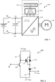
- FIG. 1 is a schematic representation of an electric drive system 100.
- Drive system 100 includes a battery 105 reversibly coupled between a high rail 110 and a low rail 115 by a switch 120.
- Drive system 100 also includes an inverter 125, an electric motor 130, and a gate drive channel 150.
- inverter 125 converts the dc voltage supplied by battery 105 into an ac voltage and supplies electric motor 130 with power.
- a DC link capacitor 135 is coupled between rails 110, 115. When battery 105 is decoupled from rails 110, 115 by switch 120, DC link capacitor 135 is discharged though inverter 125.
- switches 120 are typical mechanical switches and coupled to connect and disconnect battery 105 from rails 110, 115. Under normal conditions, battery 105 will be connected to rails 110, 115 when the vehicle that includes drive system 100 is in operation, e.g., moving or ready to move. Battery 105 will be disconnected from rails 110, 115 during shut-off or in the event of a sufficiently severe fault condition.
- both DC link capacitor 135 and inverter 125 Upon connection of battery 105 to rails 110, 115, both DC link capacitor 135 and inverter 125 will be biased by battery 105. The voltage developed across DC link capacitor 135 will tend towards equality with the voltage provided by battery 105. However, deviations from equality will occur since DC link capacitor 135 accepts and provides charge more quickly than battery 105. In addition, the DC link capacitor 135 is generally placed physically closer to the power switches of inverter 125 and some distance from the battery 105. The cable inductance could lead to high transient voltage events. DC link capacitor 135 thus acts to smooth the voltage between rails 110, 115 across inverter 125.
- Inverter 125 can include a collection of phase legs that are each formed by a pair of switching devices coupled in series between rails 110, 115.
- the switching devices will be insulated-gate bipolar transistors (IGBT) or other power semiconductor devices.
- Other power semiconductor switches could include gallium nitride (GaN), silicon (Si), or silicon carbide (SiC) based transistors.
- MOSFET metal-oxide field-effect transistors
- BJT bipolar junction transitors
- the switching of the switching devices is driven by gate driver circuitry 140 under the control of a controller 145.
- Gate driver circuitry 140 is configured to appropriately bias the switching devices in inverter 125 in accordance with control signals received from controller 145.
- Controller 145 is configured to generate the control signals in response to higher level control signals.
- Example of higher level control signals include, e.g., an indication that the vehicle's velocity is to be increased or decreased.
- gate driver circuitry 140 is referenced to rail 115.
- Controller 145 can also be referenced to rail 115, can be referenced to another voltage, or can include some components that are referenced to rail 115 and other components that are referenced to another voltage.
- gate driver circuitry 140 and controller 145 can be considered to be part of a gate drive channel 150 that controls the provision of power to electric motor 130 by appropriately driving switches in inverter 125.
- controller 145 can also switch one or more of the switching devices in inverter 125 to discharge DC link capacitor 135 when battery 105 is decoupled from rails 110, 115 by switch 120.
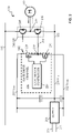
- FIG. 2 is a schematic representation of a portion of the circuitry in electric drive system 100, namely, a portion responsible for controlling the provision of power to electric motor 130 via a single phase leg.
- electric drive system 100 includes a supply 205.
- supply 205 is configured to generate an internal supply voltage (i.e., V ISO - V COM ) between its output rails 210, 212.
- Supply 205 is coupled to input rails 270, 275 and output rails 210, 212.
- high rail 110 and low rail 115 are coupled to input rails 270.
- contacts 30/31 are coupled to input rails 270, 275.
- DIN 72552 contact 30 can be coupled to input rail 270 and DIN 72552 contact 31 coupled to input rail 275.
- an intermediate output 215 with a voltage V EE that is in a range between Viso and V COM is tied to low rail 115 of battery 115.
- the intermediate output of a second supply will be tied to an intermediate node in phase leg 260 of inverter 125, i.e., output node 250.
- voltage Viso is in a voltage range suitable to drive power switch 245 and referenced to rail 115.
- voltage V COM 212 is selected to accommodate the turn-off gate voltage of IGBT 245.
- voltage V COM 212 is low with respect to the voltage on rail 115.
- V ISO , V EE , and V COM are selected to provide the turn-on and turn-off voltages for IGBT 245.
- V ISO , V EE , and V COM could be utilized to provide working supply voltages to internal circuitry in drive system 100.
- the voltage difference between V ISO and V EE can be between 10-30 V (e.g., 15 Volts).
- the voltage difference between V EE and V COM can be, e.g., > 0-10 volts (e.g., 5 volts) so that the voltage V COM on rail 212 is below the voltage on low rail 115.
- the voltage difference between rail 210, 215 (i.e., V ISO - V EE ) can be changed to discharge DC link capacitor 135 when battery 105 is decoupled from rails 110, 115.
- the illustrated implementation of a portion of gate drive channel 150 includes a gate driver controller 220, a pull up transistor 225, a pull down transistor 230, and a single gate resistor 232.
- Gate driver controller 220 is configured to receive control signals and controls transistors 225, 230 in accordance with those control signals.
- Pull up transistor 225 is coupled between high supply rail 210 and an output node 235 of the gate drive channel.
- Pull down transistor 230 is coupled between output node 235 and low rail 212.
- Gate resistor 232 conducts drive signals from output node 235 to IGBT 245.
- this portion of gate drive channel 150 can be pulled up and down using different channels that each include one transistor and one gate resistor and alternatively couple the gate of the IGBT 245 to a respective rail.
- pull up transistor 225 and pull down transistor 230 are shown as MOSFETs, respectively, it should be appreciated that other transistor devices (e.g., npn and pnp BJTs) may be used.
- the illustrated portion of electric drive system 100 also includes a single phase leg 260 of inverter 125.
- Phase leg 260 includes a pair of IGBTs 240, 245 coupled in series between positive rail 110 and low supply rail 212.
- An output node 250 of inverter 125 is between IGBTs 240, 245 and reversibly coupled to a single one of either positive rail 110 or low supply rail 115 when a respective of IGBTs 240, 245 is switched into conduction.
- control terminal (i.e., gate) of each IGBT 240, 245 is coupled to a respective portion of gate drive channel 150, although only the coupling of IGBT 245 is shown in the schematic illustration.
- inverter 125 includes additional phase legs (e.g., 3 or 4 phase legs in toto ).
- IGBT 245 When IGBT 245 is to be biased into conduction, pull down transistor 230 is driven into a non-conductive state by gate driver controller 220 and pull up transistor 225 is driven into a conductive state. Conduction through pull up transistor 225 biases IGBT 245 positively with respect to low supply rail 215 and into conduction. Current can flow through motor 130 and IGBT 245 to low supply rail 115.
- pull up transistor 225 is driven into a nonconductive state and pull down transistor 230 is driven into a conductive state by gate driver controller 220.
- Conduction through pull down transistor 230 biases the gate of IGBT 245 negatively with respect to low supply rail 115 and out of conduction. Since supply 205 supplies the voltages V ISO , V COM , low rail 212 can negatively bias the gate of IGBT 245 and ensure a proper shut-off.
- supply 205 supplies a voltage difference of 20 Volts between V ISO or rail 210 and V COM of rail 212, with V EE about 5 volts above V COM .
- the voltage difference between V ISO and V EE is thus approximately 15 Volts.
- pull down transistor 230 in conduction and pull up transistor 225 not conducting the gate of IGBT 245 will be biased to five volts below V EE -- and hence below the emitter of IGBT 245. Turn-off of IGBT 245 is insured.
- pull up transistor 225 in conduction and pull down transistor 230 not conducting the gate of IGBT 245 will be biased 15 volts positively with respect to V EE -- and 15 volts above the emitter of IGBT 245. Turn-on of IGBT 245 is insured and IGBT 245 will conduct with a given transconductance.
- FIG. 3 is a schematic representation of a portion of the circuitry in supply 205.
- FIG. 3 is a schematic representation of a portion of the circuitry in supply 205 which generates voltage V EE 215.
- the illustrated portion of supply 205 includes an input 305, a control transistor 310, Zener diodes 315, 320, a bypass transistor 325, and a resistance 330.
- input 305 is coupled to receive a signal indicative of the need to discharge DC link capacitor 135, e.g., upon shut down of the vehicle. Referenced to low rail 212, the signal received at input 305 is sufficient to bias control transistor 310 into conductance when the vehicle is operational.
- the supply 205 and the gate driver controller may be formed as part of an integrated circuit that is manufactured as either a hybrid or monolithic integrated circuit.
- the gate driver controller 220 may be implemented as an integrated circuit and the supply 205 may be implemented external from the gate drive controller 220. Or even, a portion of the supply 205 and the gate driver controller may be formed as part of an integrated circuit while other portions of the supply 205 are external to the gate driver controller.
- control transistor 310 is implemented as an NPN transistor that has a collector terminal coupled to high supply rail 210 (V ISO ) through a resistance 335 and an emitter terminal that is coupled to low rail 212 (V COM ).
- V ISO high supply rail 210
- V COM low rail 212
- control transistor 310 when the signal received at input 305 biases control transistor 310 so that it does not conduct, the voltage on the collector terminal of control transistor 310 essentially becomes equal to the voltage V ISO , i.e., essentially the entire voltage difference between high supply rail 210 and low rail 212 is across control transistor 310.
- the control terminal of bypass transistor 325 is thereby biased so that bypass transistor 325 conducts and Zener diode 315 is bypassed.
- the illustrated implementation that includes transistor 310 and resistance 335 can be used even if the amplitude of the input 305 is not large enough to turn-on transistor 325. However, in implementations where the amplitude of input 305 is large enough to turn-on transistor 325, transistor 310 and resistance 335 may be omitted.
- Zener diode 315 and bypass transistor 325 are coupled in series with Zener diodes 320 and resistance 330 to form a voltage divider between high supply rail 210 and low rail 115.
- the breakdown voltages of Zener diodes 315, 320 and the value of resistance 330 can be selected to ensure that:
- the breakdown voltages of Zener diodes 315, 320 and the value of resistance 330 can be selected to ensure that the voltage difference V ISO - V EE between high supply rail 210 and intermediate output 215 either drives IGBT 245 to conduct with a very low impedance (approximately a short circuit) or with an impedance that is sufficiently high to resist current flow.
- supply 205 can maintain voltage difference of 20 Volts between V ISO and the voltage V COM on low rail 212 with V EE about 5 volts above the voltage V COM on low rail 212.
- Zener diodes 315, 320 can each be chosen to provide a breakdown voltage of ⁇ 7.5 V. During vehicular operation with bypass transistor 325 not conducting, this provides a turn on voltage (i.e., the voltage difference between V ISO and V EE ) of 15 volts and a turn off voltage (i.e., the voltage difference between V EE and V COM ) of negative five volts.
- bypass transistor 325 bypasses Zener diode 315.
- This provides a turn on voltage (i.e., the voltage difference between V ISO and V EE ) of 7.5 volts and a turn off voltage (i.e., the voltage difference between V EE and V ISO ) of approximately negative 12.5 volts.
- the transition to begin discharge of DC link capacitor 135 can be initiated in response to, e.g., the same signal that opens switch 120.
- Gate driver channel 150 can stop driving the switches in inverter 125.
- the high-side switch in each respective phase leg e.g., IGBT 240 in phase leg 260
- bypass transistor 325 can be switched into conductance, resulting in a voltage difference between high supply rail 210 and intermediate output 215 (i.e., V ISO -V EE ) that suffices to drive IGBT 245 with a limited transconductance.
- supply 205 can further include a voltage buffer (e.g., a unity gain operational amplifier voltage follower) between the anode of Zener diode 320 and intermediate output 215. If such an operational amplifier can source/sink relatively large currents, then the voltage on intermediate output 215 can follow the voltage on the anode of Zener diode 320 more quickly.
- a suitable transition time would be approximately 5% to 20% of requested discharge time (e.g. 100 ms to 400 ms for a discharge time of 2 s).
- the gate driver controller can be controlled to pulse the control terminal of IGBT 245 with a series of pulses that each only suffice to bias IGBT 245 into conduction with a limited transconductance.
- the pulses can be width modulated to as to discharge DC link capacitor 135 with a desired waveform.
- DC link capacitor 135 In response to the voltage across DC link capacitor 135 dropping below a predefined level (e.g., 60 V or other level specified by an appropriate regulatory agency), the active discharge of DC link capacitor 135 can be stopped. For example, both the pulsing of the low-side switches in the different phase legs and the driving of the high-side switches in the different phase legs can be stopped. Further, bypass transistor 325 need not be biased to conduct.
- a predefined level e.g. 60 V or other level specified by an appropriate regulatory agency
- the low-side switches can be driven to conduct with a high transconductance and the high-side switches can be pulsed.
- both the high-side and low-side switches can be pulsed-either in synch or asynchronously.
- only a proper subset of the phase legs need participate in active discharge of DC link capacitor 135. In all of these cases, an appropriate voltage for pulsing the respective switches can be achieved by tailoring the voltages provided by a supply.
- FIG. 4 is a graph 400 that represents the output characteristics of an IGBT that is suitable for use an inverter in an electric vehicle drive system, e.g., as IGBT's 240, 245.
- Position along the x-axis in graph 400 denotes the voltage difference between the collector and the emitter (i.e., V CE ) of the IGBT in volts.
- Position along the y-axis denotes the collector current (i.e., Ic) in amperes.
- the different curves 405, 410, 415, 420, 425, 430 are each associated with a different voltage between the gate and the emitter of the IGBT (i.e., V GE ).
- curve 405 shows the relationship between V CE and Ic when V GE is 19 Volts
- curve 410 shows the relationship between V CE and Ic when V GE is 17 Volts
- curve 415 shows the relationship between V CE and Ic when V GE is 15 Volts
- curve 420 shows the relationship between V CE and Ic when V GE is 13 Volts
- curve 425 shows the relationship between V CE and Ic when V GE is 11 Volts
- curve 430 shows the relationship between V CE and Ic when V GE is 9 Volts.
- the slope of curves 405, 410, 415, 420, 425, 430 decreases and the resistance of the IGBT increases.
- graphs like graph 400 are provided by the supplier of an IGBT can be readily used to tailor the voltages and the values of different components to a particular set of operational circumstances.
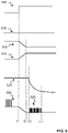
- FIG. 5 is a schematic representation of different waveforms in an electric drive system 100.
- the waveforms are all presented as a function of time and span a window during which the voltage across DC link capacitor 135 is discharged.
- the waveforms can span a short window during and shortly after shut down or a response to a sufficiently severe fault condition.
- Waveform 505 represents the voltage applied to the gate of bypass transistor 325.
- Waveform 510 represents the regulated voltage V ISO at high supply rail 210 relative to the voltage V COM on low rail 212.
- Waveform 515 represents the voltage difference between the voltage V ISO at high supply rail 210 and the voltage V EE at intermediate output 215.
- Waveform 520 represents the voltage difference between the voltage V EE at intermediate output215 and the voltage V COM at low rail 212.
- Waveform 525 represents the voltage across DC link capacitor 135.
- Waveform 530 represents the gate-to-emitter voltage of IGBT 245 (or other IGBT that participates in active discharge of DC link capacitor 135).
- bypass transistor 325 Prior to time T1, the voltage applied to the gate of bypass transistor 325, i.e., waveform 505 is low and bypass transistor 325 remains in a non-conductive state.
- the voltage V ISO - V COM i.e., waveform 510 is regulated to a constant value-as it is throughout the illustrated time window.
- the voltage difference between the voltage at high supply rail 210 and the voltage at intermediate output 215, i.e., V ISO - V EE as represented by waveform 515, is relatively high.
- the voltage difference between the voltage V EE at intermediate output 215 and the voltage at low rail 212, i.e., V EE -V COM as represented by waveform 520, is relatively low.
- the voltage V EE on intermediate output 215 is sufficiently lower that the voltage V ISO on high supply rail 210 such that application of the voltage V ISO on high supply rail 210 to output node 235 and the control terminal of IGBT 245 suffices to drive IGBT 245 with a high transconductance.
- the voltage across DC link capacitor 135, i.e., waveform 525 is high and approximately equal to the dc voltage provided by battery 105.
- the gate-to-emitter voltage of the IGBT, i.e., waveform 530 includes a collection of relatively large amplitude pulses that represent the driving of motor 130.
- discharge of DC link capacitor 135 is triggered, e.g., by vehicle shut down or a sufficiently severe fault condition.
- the voltage applied to the gate of bypass transistor 325, i.e., waveform 505 rises and bypass transistor 325 is biased into a conductive state.
- the voltage difference between the voltage V ISO at high supply rail 210 and the voltage V EE at intermediate output 215, i.e., waveform 515 begins to fall and eventually settles at a time T2.
- the voltage difference between the voltage V EE at intermediate output 215 and the voltage at low rail 212, i.e., waveform 520 begins to rise and eventually settles at a time T2.
- the voltage across DC link capacitor 135, i.e., waveform 525 remains high but may decrease slightly, e.g., due to parasitic or other power consumption by various components.
- the gate-to-emitter voltage of the IGBT i.e., waveform 530, falls in conjunction with the increase in the voltage V EE at intermediate output 215.
- the gate-to-emitter voltage of the IGBT i.e., waveform 530
- the gate-to-emitter voltage of the IGBT is pulsed with a series of pulses 535 that each only suffice to bias IGBT 245 into conduction with a limited transconductance.
- the voltage across DC link capacitor 135, i.e., waveform 525 discharges while the other waveforms remain unchanged.
- the voltage across DC link capacitor 135 has fallen to a sufficiently low level that active discharge using pulses 535 can be ended.
- the voltage across DC link capacitor 135 can continue to fall over time due to power consumption by other components.
- waveforms 505, 510, 515, 520, 525, 530 only span a short window during and shortly after shut down or a response to a sufficiently severe fault condition.
- a complete shut down or response can include, e.g., ending the application of a voltage to the gate of bypass transistor 325, ending regulation of the voltage difference V ISO - V COM , and completion of the discharge of the voltage across DC link capacitor 135. For the sake of brevity, a complete shut down or response is not shown.
Landscapes
- Engineering & Computer Science (AREA)
- Power Engineering (AREA)
- Mechanical Engineering (AREA)
- Transportation (AREA)
- Life Sciences & Earth Sciences (AREA)
- Sustainable Energy (AREA)
- Sustainable Development (AREA)
- Physics & Mathematics (AREA)
- Nonlinear Science (AREA)
- Automation & Control Theory (AREA)
- Radar, Positioning & Navigation (AREA)
- General Physics & Mathematics (AREA)
- Electromagnetism (AREA)
- Inverter Devices (AREA)
Priority Applications (3)
| Application Number | Priority Date | Filing Date | Title |
|---|---|---|---|
| EP21157846.3A EP4046849A1 (fr) | 2021-02-18 | 2021-02-18 | Décharge active d'un système d'entraînement électrique |
| US17/581,777 US12227086B2 (en) | 2021-02-18 | 2022-01-21 | Active discharge of an electric drive system |
| CN202210163367.XA CN114977865A (zh) | 2021-02-18 | 2022-02-18 | 电驱动系统的有源放电 |
Applications Claiming Priority (1)
| Application Number | Priority Date | Filing Date | Title |
|---|---|---|---|
| EP21157846.3A EP4046849A1 (fr) | 2021-02-18 | 2021-02-18 | Décharge active d'un système d'entraînement électrique |
Publications (1)
| Publication Number | Publication Date |
|---|---|
| EP4046849A1 true EP4046849A1 (fr) | 2022-08-24 |
Family
ID=74668683
Family Applications (1)
| Application Number | Title | Priority Date | Filing Date |
|---|---|---|---|
| EP21157846.3A Pending EP4046849A1 (fr) | 2021-02-18 | 2021-02-18 | Décharge active d'un système d'entraînement électrique |
Country Status (3)
| Country | Link |
|---|---|
| US (1) | US12227086B2 (fr) |
| EP (1) | EP4046849A1 (fr) |
| CN (1) | CN114977865A (fr) |
Families Citing this family (4)
| Publication number | Priority date | Publication date | Assignee | Title |
|---|---|---|---|---|
| EP4046849A1 (fr) | 2021-02-18 | 2022-08-24 | Power Integrations, Inc. | Décharge active d'un système d'entraînement électrique |
| EP4046850B1 (fr) * | 2021-02-18 | 2025-09-24 | Power Integrations, Inc. | Décharge active d'un système d'entraînement électrique |
| EP4186733B1 (fr) | 2021-11-24 | 2025-01-01 | Power Integrations, Inc. | Décharge active d'un système d'entraînement électrique |
| WO2025213461A1 (fr) * | 2024-04-12 | 2025-10-16 | Wolfspeed, Inc. | Générateur rapide de tension négative configuré pour une mise en œuvre avec une attaque de grille d'un dispositif de puissance et son procédé de mise en œuvre |
Citations (4)
| Publication number | Priority date | Publication date | Assignee | Title |
|---|---|---|---|---|
| US20110221370A1 (en) * | 2010-03-11 | 2011-09-15 | Denso Corporation | Discharge control device for power conversion system |
| DE112011105295B4 (de) * | 2011-05-31 | 2017-02-09 | Toyota Jidosha Kabushiki Kaisha | Fahrzeug mit einer elektrischen Antriebsvorrichtung und einer Entladungsschaltung sowie Steuerverfahren hierfür |
| US20180219546A1 (en) * | 2017-01-31 | 2018-08-02 | Ford Global Technologies, Llc | Resonant gate driver |
| US10183555B2 (en) * | 2013-11-20 | 2019-01-22 | Denso Corporation | Onboard electric system |
Family Cites Families (46)
| Publication number | Priority date | Publication date | Assignee | Title |
|---|---|---|---|---|
| JP2680914B2 (ja) | 1990-05-10 | 1997-11-19 | 甲府日本電気株式会社 | スイッチング電源回路 |
| US7109686B2 (en) * | 2004-11-15 | 2006-09-19 | Ise Corporation | System and method for precharging and discharging a high power ultracapacitor pack |
| US7158393B2 (en) | 2005-03-11 | 2007-01-02 | Soft Switching Technologies Corporation | Power conversion and voltage sag correction with regenerative loads |
| US7368890B2 (en) | 2006-02-07 | 2008-05-06 | Rockwell Automation Technologies, Inc. | Power converter with active discharging for improved auto-restart capability |
| JP2008061300A (ja) | 2006-08-29 | 2008-03-13 | Toyota Motor Corp | 電力変換装置およびその電力変換装置における残留電荷の消費方法 |
| US8140204B2 (en) * | 2007-12-10 | 2012-03-20 | Ford Global Technologies, Llc | Charge depleting energy management strategy for plug-in hybrid electric vehicles |
| JP2009232620A (ja) | 2008-03-24 | 2009-10-08 | Toshiba Mitsubishi-Electric Industrial System Corp | 電力変換装置 |
| US8039993B2 (en) | 2008-04-24 | 2011-10-18 | GM Global Technology Operations LLC | High-voltage bus discharge with logarithmic self-protection |
| US7635998B1 (en) | 2008-07-10 | 2009-12-22 | Freescale Semiconductor, Inc. | Pre-driver for bridge circuit |
| US8022569B2 (en) * | 2008-10-23 | 2011-09-20 | GM Global Technology Operations LLC | Systems and methods for discharging bus voltage using semiconductor devices |
| US8115457B2 (en) | 2009-07-31 | 2012-02-14 | Power Integrations, Inc. | Method and apparatus for implementing a power converter input terminal voltage discharge circuit |
| JP4835743B2 (ja) | 2009-10-07 | 2011-12-14 | 株式会社デンソー | 電力変換回路の制御装置 |
| US8299730B2 (en) | 2010-02-09 | 2012-10-30 | Power Integrations, Inc. | Integrated on-time extension for non-dissipative bleeding in a power supply |
| JP5064547B2 (ja) | 2010-09-15 | 2012-10-31 | 豊田合成株式会社 | 車両用放電装置 |
| US8610382B2 (en) | 2010-12-23 | 2013-12-17 | Caterpillar Inc. | Active high voltage bus bleed down |
| DE102011083945A1 (de) | 2011-10-04 | 2013-04-04 | Robert Bosch Gmbh | Steuervorrichtung für Halbleiterschalter eines Wechselrichters und Verfahren zum Ansteuern eines Wechselrichters |
| DE102012202869B4 (de) | 2012-02-24 | 2024-10-02 | Robert Bosch Gmbh | Ansteuervorrichtung und Ansteuerverfahren einer aktiven Snubberschaltung für einen Gleichspannungswandler |
| US9018865B2 (en) * | 2012-04-30 | 2015-04-28 | GM Global Technology Operations LLC | Passive high-voltage DC bus discharge circuit for a vehicle |
| US9041329B2 (en) * | 2012-09-19 | 2015-05-26 | Ford Global Technologies, Llc | Vehicle electric machine control strategy |
| WO2014159456A1 (fr) | 2013-03-12 | 2014-10-02 | Power Integrations, Inc. | Régulateur de courant intégré permettant d'entretenir un courant de maintien d'un circuit atténuateur |
| EP3017542B1 (fr) * | 2013-07-04 | 2019-09-11 | NXP USA, Inc. | Circuit d'attaque de gâchette et procédé de commande d'un transistor de puissance |
| US9484814B2 (en) | 2014-11-07 | 2016-11-01 | Power Integrations, Inc. | Power converter controller with analog controlled variable current circuit |
| US9219420B1 (en) | 2014-11-07 | 2015-12-22 | Power Integrations, Inc. | Overvoltage protection using a tapFET |
| US10351002B2 (en) | 2014-11-14 | 2019-07-16 | Aisin Aw Co., Ltd. | Inverter control device and vehicle control device |
| GB2545236B (en) | 2015-12-10 | 2017-12-13 | Rolls Royce Plc | A method of controlling an inverter |
| US9985452B2 (en) | 2016-03-03 | 2018-05-29 | GM Global Technology Operations LLC | Apparatus for discharging a high-voltage bus |
| ITUA20161431A1 (it) | 2016-03-07 | 2017-09-07 | St Microelectronics Srl | Circuito di pilotaggio di gate per uno stadio di uscita half bridge o full bridge e corrispondente procedimento per pilotare uno stadio di uscita half bridge o full bridge |
| US9748947B1 (en) | 2016-07-12 | 2017-08-29 | Ge Energy Power Conversion Technology Ltd | IGBT gate drive circuit and method |
| US10384561B2 (en) | 2016-09-19 | 2019-08-20 | Ford Global Technologies, Llc | Active discharge circuit for link capacitor using phase leg switches |
| US9954461B1 (en) | 2017-06-12 | 2018-04-24 | Power Integrations, Inc. | Multiple stage gate drive for cascode current sensing |
| US10644581B2 (en) | 2017-11-01 | 2020-05-05 | Texas Instruments Incorporated | DC-DC power conversion circuitry with efficiency optimization using temperature sensing |
| DE102018204382A1 (de) | 2018-03-22 | 2019-09-26 | Audi Ag | Zwischenkreiskondensator für ein elektromotorisch angetriebenes Fahrzeug |
| US10924001B2 (en) | 2018-08-22 | 2021-02-16 | Texas Instruments Incorporated | Gate driver controller and associated discharge method |
| CN109600030B (zh) | 2018-10-12 | 2021-03-23 | 蔚来(安徽)控股有限公司 | 用于功率装置的母线电容放电方法、系统及装置 |
| JP7156996B2 (ja) | 2019-04-24 | 2022-10-19 | 本田技研工業株式会社 | 車両の電源システム |
| KR102726797B1 (ko) | 2019-06-17 | 2024-11-05 | 현대자동차주식회사 | 전력변환장치용 스위칭소자의 구동 제어 장치 및 방법 |
| EP3987648A1 (fr) | 2019-08-05 | 2022-04-27 | Siemens Energy Global GmbH & Co. KG | Convertisseur de puissance |
| US10998843B2 (en) | 2019-09-23 | 2021-05-04 | Power Integrations, Inc. | External adjustment of a drive control of a switch |
| US10790818B1 (en) * | 2019-09-27 | 2020-09-29 | Infineon Technologies Austria Ag | Slew rate control by adaptation of the gate drive voltage of a power transistor |
| EP3975402B1 (fr) | 2020-09-29 | 2024-04-17 | STMicroelectronics S.r.l. | Circuit de commande de décharge, système, véhicule et procédé correspondants |
| DE102021122687A1 (de) | 2020-12-02 | 2022-06-02 | Hanon Systems | Anordnung und Verfahren zur Entladung eines Zwischenkreiskondensators |
| US11437911B2 (en) | 2020-12-22 | 2022-09-06 | Power Integrations, Inc. | Variable drive strength in response to a power converter operating condition |
| DE102021103299A1 (de) | 2021-02-12 | 2022-08-18 | Bayerische Motoren Werke Aktiengesellschaft | Aktives Entladen eines Drei-Phasen-Wechselrichters |
| EP4046849A1 (fr) | 2021-02-18 | 2022-08-24 | Power Integrations, Inc. | Décharge active d'un système d'entraînement électrique |
| US12351037B2 (en) | 2023-02-22 | 2025-07-08 | Eaton Intelligent Power Limited | Thermal management of active discharge function in automotive inverters |
| IT202300004365A1 (it) | 2023-03-09 | 2024-09-09 | St Microelectronics Int Nv | Circuito di pilotaggio con controllo di scarica, sistema elettronico e veicolo corrispondenti |
-
2021
- 2021-02-18 EP EP21157846.3A patent/EP4046849A1/fr active Pending
-
2022
- 2022-01-21 US US17/581,777 patent/US12227086B2/en active Active
- 2022-02-18 CN CN202210163367.XA patent/CN114977865A/zh active Pending
Patent Citations (4)
| Publication number | Priority date | Publication date | Assignee | Title |
|---|---|---|---|---|
| US20110221370A1 (en) * | 2010-03-11 | 2011-09-15 | Denso Corporation | Discharge control device for power conversion system |
| DE112011105295B4 (de) * | 2011-05-31 | 2017-02-09 | Toyota Jidosha Kabushiki Kaisha | Fahrzeug mit einer elektrischen Antriebsvorrichtung und einer Entladungsschaltung sowie Steuerverfahren hierfür |
| US10183555B2 (en) * | 2013-11-20 | 2019-01-22 | Denso Corporation | Onboard electric system |
| US20180219546A1 (en) * | 2017-01-31 | 2018-08-02 | Ford Global Technologies, Llc | Resonant gate driver |
Also Published As
| Publication number | Publication date |
|---|---|
| US20220258610A1 (en) | 2022-08-18 |
| US12227086B2 (en) | 2025-02-18 |
| CN114977865A (zh) | 2022-08-30 |
Similar Documents
| Publication | Publication Date | Title |
|---|---|---|
| US12227086B2 (en) | Active discharge of an electric drive system | |
| EP0649579B1 (fr) | Circuit de commande d'un demi-pont | |
| EP3745466A1 (fr) | Circuit d'excursion basse intégré à sécurité intégrée pour commutateur gan | |
| KR101723358B1 (ko) | 스위칭 소자 구동 회로, 파워 모듈 및 자동차 | |
| CN104467370B (zh) | 用于隔离的驱动器的软关闭的设备和方法 | |
| US9264022B2 (en) | Level shift circuit | |
| US12323052B2 (en) | Active discharge of an electric drive system | |
| US11695321B2 (en) | Gate drive adapter | |
| US20210288640A1 (en) | Semiconductor Device Signal Transmission Circuit for Drive-Control, Method of Controlling Semiconductor Device Signal Transmission Circuit for Drive-Control, Semiconductor Device, Power Conversion Device, and Electric System for Railway Vehicle | |
| US20190229721A1 (en) | Minimizing ringing in wide band gap semiconductor devices | |
| CN113497546B (zh) | 栅极驱动装置及栅极驱动方法、功率半导体模块和电力变换装置 | |
| KR20240034826A (ko) | 반도체 구동 장치 및 그것을 구비하는 전력 변환 장치 | |
| US20250266754A1 (en) | Active discharge of an electric drive system | |
| JP2023134570A (ja) | 出力トランジスタの駆動回路、半導体装置、自動車 | |
| US12407342B2 (en) | Drive circuit to drive power semiconductor element, power semiconductor module, and power conversion device | |
| Zhou et al. | A low cost gate driver with dynamic turn-off transient control for HEV/EV traction inverter application | |
| CN116780864A (zh) | 开关元件的驱动电路和智能功率模块 | |
| WO2024018612A1 (fr) | Dispositif à semi-conducteur et dispositif de conversion de puissance | |
| CN115708301A (zh) | 驱动装置 | |
| WO2025133712A1 (fr) | Interrupteurs d'attaque à courants variables | |
| CN119766212A (zh) | 一种开关功率管截止控制电路及驱动芯片 | |
| WO2023162032A1 (fr) | Circuit d'attaque de grille et dispositif de conversion de puissance utilisant ledit circuit |
Legal Events
| Date | Code | Title | Description |
|---|---|---|---|
| PUAI | Public reference made under article 153(3) epc to a published international application that has entered the european phase |
Free format text: ORIGINAL CODE: 0009012 |
|
| STAA | Information on the status of an ep patent application or granted ep patent |
Free format text: STATUS: REQUEST FOR EXAMINATION WAS MADE |
|
| 17P | Request for examination filed |
Effective date: 20210218 |
|
| AK | Designated contracting states |
Kind code of ref document: A1 Designated state(s): AL AT BE BG CH CY CZ DE DK EE ES FI FR GB GR HR HU IE IS IT LI LT LU LV MC MK MT NL NO PL PT RO RS SE SI SK SM TR |
|
| STAA | Information on the status of an ep patent application or granted ep patent |
Free format text: STATUS: EXAMINATION IS IN PROGRESS |
|
| 17Q | First examination report despatched |
Effective date: 20260313 |