EP4040476A1 - Photodetector - Google Patents
Photodetector Download PDFInfo
- Publication number
- EP4040476A1 EP4040476A1 EP20871226.5A EP20871226A EP4040476A1 EP 4040476 A1 EP4040476 A1 EP 4040476A1 EP 20871226 A EP20871226 A EP 20871226A EP 4040476 A1 EP4040476 A1 EP 4040476A1
- Authority
- EP
- European Patent Office
- Prior art keywords
- hole
- light receiving
- side wall
- receiving element
- end portion
- Prior art date
- Legal status (The legal status is an assumption and is not a legal conclusion. Google has not performed a legal analysis and makes no representation as to the accuracy of the status listed.)
- Withdrawn
Links
Images


Classifications
-
- H—ELECTRICITY
- H10—SEMICONDUCTOR DEVICES; ELECTRIC SOLID-STATE DEVICES NOT OTHERWISE PROVIDED FOR
- H10F—INORGANIC SEMICONDUCTOR DEVICES SENSITIVE TO INFRARED RADIATION, LIGHT, ELECTROMAGNETIC RADIATION OF SHORTER WAVELENGTH OR CORPUSCULAR RADIATION
- H10F39/00—Integrated devices, or assemblies of multiple devices, comprising at least one element covered by group H10F30/00, e.g. radiation detectors comprising photodiode arrays
- H10F39/80—Constructional details of image sensors
- H10F39/804—Containers or encapsulations
-
- H—ELECTRICITY
- H10—SEMICONDUCTOR DEVICES; ELECTRIC SOLID-STATE DEVICES NOT OTHERWISE PROVIDED FOR
- H10F—INORGANIC SEMICONDUCTOR DEVICES SENSITIVE TO INFRARED RADIATION, LIGHT, ELECTROMAGNETIC RADIATION OF SHORTER WAVELENGTH OR CORPUSCULAR RADIATION
- H10F77/00—Constructional details of devices covered by this subclass
- H10F77/93—Interconnections
-
- H—ELECTRICITY
- H10—SEMICONDUCTOR DEVICES; ELECTRIC SOLID-STATE DEVICES NOT OTHERWISE PROVIDED FOR
- H10F—INORGANIC SEMICONDUCTOR DEVICES SENSITIVE TO INFRARED RADIATION, LIGHT, ELECTROMAGNETIC RADIATION OF SHORTER WAVELENGTH OR CORPUSCULAR RADIATION
- H10F39/00—Integrated devices, or assemblies of multiple devices, comprising at least one element covered by group H10F30/00, e.g. radiation detectors comprising photodiode arrays
- H10F39/10—Integrated devices
- H10F39/12—Image sensors
-
- H—ELECTRICITY
- H10—SEMICONDUCTOR DEVICES; ELECTRIC SOLID-STATE DEVICES NOT OTHERWISE PROVIDED FOR
- H10F—INORGANIC SEMICONDUCTOR DEVICES SENSITIVE TO INFRARED RADIATION, LIGHT, ELECTROMAGNETIC RADIATION OF SHORTER WAVELENGTH OR CORPUSCULAR RADIATION
- H10F39/00—Integrated devices, or assemblies of multiple devices, comprising at least one element covered by group H10F30/00, e.g. radiation detectors comprising photodiode arrays
- H10F39/80—Constructional details of image sensors
- H10F39/811—Interconnections
-
- H—ELECTRICITY
- H10—SEMICONDUCTOR DEVICES; ELECTRIC SOLID-STATE DEVICES NOT OTHERWISE PROVIDED FOR
- H10F—INORGANIC SEMICONDUCTOR DEVICES SENSITIVE TO INFRARED RADIATION, LIGHT, ELECTROMAGNETIC RADIATION OF SHORTER WAVELENGTH OR CORPUSCULAR RADIATION
- H10F77/00—Constructional details of devices covered by this subclass
- H10F77/50—Encapsulations or containers
-
- H—ELECTRICITY
- H10—SEMICONDUCTOR DEVICES; ELECTRIC SOLID-STATE DEVICES NOT OTHERWISE PROVIDED FOR
- H10W—GENERIC PACKAGES, INTERCONNECTIONS, CONNECTORS OR OTHER CONSTRUCTIONAL DETAILS OF DEVICES COVERED BY CLASS H10
- H10W42/00—Arrangements for protection of devices
-
- H—ELECTRICITY
- H10—SEMICONDUCTOR DEVICES; ELECTRIC SOLID-STATE DEVICES NOT OTHERWISE PROVIDED FOR
- H10W—GENERIC PACKAGES, INTERCONNECTIONS, CONNECTORS OR OTHER CONSTRUCTIONAL DETAILS OF DEVICES COVERED BY CLASS H10
- H10W72/00—Interconnections or connectors in packages
- H10W72/50—Bond wires
-
- H—ELECTRICITY
- H10—SEMICONDUCTOR DEVICES; ELECTRIC SOLID-STATE DEVICES NOT OTHERWISE PROVIDED FOR
- H10W—GENERIC PACKAGES, INTERCONNECTIONS, CONNECTORS OR OTHER CONSTRUCTIONAL DETAILS OF DEVICES COVERED BY CLASS H10
- H10W76/00—Containers; Fillings or auxiliary members therefor; Seals
- H10W76/10—Containers or parts thereof
- H10W76/12—Containers or parts thereof characterised by their shape
-
- H—ELECTRICITY
- H10—SEMICONDUCTOR DEVICES; ELECTRIC SOLID-STATE DEVICES NOT OTHERWISE PROVIDED FOR
- H10W—GENERIC PACKAGES, INTERCONNECTIONS, CONNECTORS OR OTHER CONSTRUCTIONAL DETAILS OF DEVICES COVERED BY CLASS H10
- H10W76/00—Containers; Fillings or auxiliary members therefor; Seals
- H10W76/10—Containers or parts thereof
- H10W76/17—Containers or parts thereof characterised by their materials
- H10W76/18—Insulating materials, e.g. resins, glasses or ceramics
-
- H—ELECTRICITY
- H10—SEMICONDUCTOR DEVICES; ELECTRIC SOLID-STATE DEVICES NOT OTHERWISE PROVIDED FOR
- H10W—GENERIC PACKAGES, INTERCONNECTIONS, CONNECTORS OR OTHER CONSTRUCTIONAL DETAILS OF DEVICES COVERED BY CLASS H10
- H10W72/00—Interconnections or connectors in packages
- H10W72/851—Dispositions of multiple connectors or interconnections
- H10W72/874—On different surfaces
- H10W72/884—Die-attach connectors and bond wires
Definitions
- the present disclosure relates to a photodetector.
- a photodetector including a light receiving element and a package accommodating the light receiving element, in which the package includes an accommodation member formed of a ceramic and a light transmitting member attached to the accommodation member such that an opening of a recess portion of the accommodation member is covered, is known (for example, refer to Patent Literature 1).
- An accommodation member formed of a ceramic has excellent heat dissipation and heat resistance compared to an accommodation member formed of a resin, for example.
- Patent Literature 1 Japanese Unexamined Patent Publication No. 2015-216142
- An object of the present disclosure is to provide a photodetector in which electrical connection between a wiring provided in a package and a light receiving element accommodated inside the package can be reliably performed and occurrence of dew condensation inside the package can be reliably prevented.
- a photodetector includes a light receiving element provided with a light receiving portion and a terminal, and a package accommodating the light receiving element.
- the package has an accommodation member including a bottom wall and a side wall defining an opening facing the bottom wall, the accommodation member formed of a ceramic, a wiring including a pad connected to the terminal by a wire, the wiring provided in the accommodation member, and a light transmitting member attached to the side wall such that the opening is covered.
- the bottom wall has a placement surface to which the light receiving element is attached by an adhesive member.
- the bottom wall or the side wall has a pad surface on which the pad is disposed, the pad surface positioned on the opening side with respect to the placement surface.
- the side wall has a through hole allowing communication between the inside of the package and the outside of the package. At least a portion of an inner end portion of the through hole is positioned on the opening side with respect to a surface of the light receiving element on the opening side.
- the pad surface on which the pad of the wiring is disposed is positioned on the opening side of the accommodation member with respect to the placement surface to which the light receiving element is attached by the adhesive member. Accordingly, the adhesive member is unlikely to reach the pad surface. Therefore, the terminal and the pad for the wiring corresponding to each other in the light receiving element are reliably connected to each other by the wire.
- the accommodation member formed of a ceramic at least a portion of the inner end portion of the through hole formed in the side wall is positioned on the opening side of the accommodation member with respect to the surface of the light receiving element on the opening side.
- the inner end portion of the through hole is unlikely to be blocked by the adhesive member. Therefore, ventilation between the inside and the outside of the package is secured, and occurrence of dew condensation inside the package is reliably prevented.
- electrical connection between the wiring provided in the package and the light receiving element accommodated inside the package can be reliably performed, and occurrence of dew condensation inside the package can be reliably prevented.
- At least a portion of the inner end portion of the through hole may be positioned on the opening side with respect to the pad surface. Accordingly, even if a foreign substance intrudes into the package through the through hole, the foreign substance can be easily captured on the pad surface. Moreover, the light receiving portion of the light receiving element is separated from the inner end portion of the through hole by an amount corresponding to a thickness of the pad surface therebetween. Hence, even if a foreign substance intrudes into the package through the through hole, arrival of the foreign substance at the light receiving portion of the light receiving element can be curbed.
- the through hole may have a bent portion. Accordingly, intrusion of a foreign substance into the package through the through hole can be curbed.
- an internal surface of the through hole may exhibit a rounded shape at the bent portion. Accordingly, the accommodation member is unlikely to break at the bent portion. Therefore, intrusion of a foreign substance into the package caused by such breakage can be curbed.
- the through hole may be a single hole. Accordingly, compared to when there are a plurality of through holes, intrusion of a foreign substance into the package through the through hole can be curbed.
- an inner surface of the side wall may have an inside corner portion when viewed in a direction in which the bottom wall and the opening face each other.
- the inner end portion of the through hole may be positioned at the inside corner portion. Accordingly, smooth ventilation between the inside and the outside of the package can be achieved.
- the side wall may have a corner portion when viewed in a direction in which the bottom wall and the opening face each other.
- the through hole may be formed at the corner portion. Accordingly, a length of the through hole can be increased, and intrusion of a foreign substance into the package through the through hole can be curbed.
- the side wall may include a plurality of side wall portions.
- An outer end portion of the through hole may be positioned on an outer surface of a side wall portion having the largest thickness of the plurality of side wall portions. Accordingly, the length of the through hole can be increased, and intrusion of a foreign substance into the package through the through hole can be curbed.
- a recess portion may be formed on an outer surface of the side wall.
- An outer end portion of the through hole may be positioned in the recess portion. Accordingly, intrusion of a foreign substance into the outer end portion of the through hole can be curbed.
- the wiring may include a plurality of connection portions extending in a direction in which the bottom wall and the opening face each other on an outer surface of the side wall.
- a distance between a connection portion closest to the outer end portion of the through hole of the plurality of connection portions and the outer end portion of the through hole may be longer than a distance between the connection portion closest to the outer end portion of the through hole of the plurality of connection portions and a connection portion second closest to the outer end portion of the through hole of the plurality of connection portions. Accordingly, blocking of the outer end portion of the through hole by a reflow material which has melted when the photodetector is mounted can be curbed.
- a center position of the light receiving portion may coincide with a center position of the package in at least a predetermined direction when viewed in a direction in which the bottom wall and the opening face each other. Accordingly, when the photodetector is mounted, positioning of the light receiving portion can be performed based on the package in at least a predetermined direction.
- the inner end portion of the through hole may be positioned on a side opposite to the center position of the light receiving portion with respect to the center position of the package in at least a predetermined direction when viewed in a direction in which the bottom wall and the opening face each other. Accordingly, the light receiving portion of the light receiving element is separated from the inner end portion of the through hole in at least a predetermined direction. Therefore, even if a foreign substance intrudes into the package through the through hole, arrival of the foreign substance at the light receiving portion of the light receiving element can be curbed.
- a gap may be formed between the light receiving element and the side wall. Accordingly, even if a foreign substance intrudes into the package through the through hole, the foreign substance can be easily captured by the gap between the light receiving element and the side wall. Therefore, arrival of a foreign substance at the light receiving portion of the light receiving element can be curbed.
- a height difference between the surface of the light receiving element on the opening side and the pad surface may be smaller than a thickness of the light receiving element. Accordingly, connection of the wire to the terminal of the light receiving element and the pad of the wiring corresponding to each other can be easily performed.
- a photodetector in which electrical connection between a wiring provided in a package and a light receiving element accommodated inside the package can be reliably performed and occurrence of dew condensation inside the package can be reliably prevented.
- a photodetector 1 includes a light receiving element 2 and a package 3 accommodating the light receiving element 2.
- the package 3 has an accommodation member 4, a plurality of wirings 5, and a light transmitting member 6.
- an incident direction of light with respect to the photodetector 1 will be referred to as a Z direction
- a direction perpendicular to the Z direction will be referred to as an X direction
- a direction perpendicular to both the Z direction and the X direction will be referred to as a Y direction.
- the light receiving element 2 is a rear incident-type solid state imaging element (for example, a CMOS image sensor).
- the light receiving element 2 exhibits a rectangular plate shape having each of the X direction and the Y direction as an extending direction of each side and having the Z direction as a thickness direction thereof.
- a length of each side of the light receiving element 2 is approximately around ten mm, and a thickness of the light receiving element 2 is approximately several hundred ⁇ m.
- the light receiving element 2 is provided with a light receiving portion 21 and a plurality of terminals 22.
- the light receiving portion 21 exhibits a rectangular shape having each of the X direction and the Y direction as an extending direction of each side.
- a length of each side of the light receiving portion 21 is approximately several mm to around ten mm.
- the light receiving portion 21 is offset to one side in the X direction (the left side in FIG. 1 ) and one side in the Y direction (the upper side in FIG. 1 ).
- Regions other than the light receiving portion 21 in the light receiving element 2 is provided with circuits such as a CMOS reading circuit, a vertical scanning circuit, and a horizontal scanning circuit (not illustrated).
- the plurality of terminals 22 are disposed along an outer edge of a surface 2a of the light receiving element 2. Each of the terminals 22 is buried on the surface 2a in an exposed state on the surface 2a. Each of the terminals 22 is electrically connected to the circuits of the light receiving element 2.
- the accommodation member 4 includes a bottom wall 41 and a side wall 42 and is formed of a ceramic.
- the bottom wall 41 and the side wall 42 are integrally formed by sintering of a laminate.
- the bottom wall 41 is a part between a flat surface including a placement surface 41a (which will be described below) and an outer surface 41b in the accommodation member 4.
- the bottom wall 41 exhibits a rectangular plate shape having each of the X direction and the Y direction as an extending direction of each side and having the Z direction as a thickness direction thereof.
- a length of each side of the bottom wall 41 is approximately around ten mm, and a thickness of the bottom wall 41 (that is, a distance between a flat surface including the placement surface 41a and the outer surface 41b) is approximately several hundred ⁇ m.
- the side wall 42 defines an opening 40 facing the bottom wall 41 in the Z direction.
- the side wall 42 exhibits a rectangular frame shape extending along an outer edge of the bottom wall 41.
- a height of the side wall 42 is approximately several hundred ⁇ m, and a thickness of the side wall 42 is approximately several mm.
- the side wall 42 is constituted of a plurality of side wall portions 43, 44, 45, and 46.
- the side wall portion 43 is positioned on one side in the X direction (the left side in FIG. 1 ).
- the side wall portion 44 is positioned on the other side in the X direction (the right side in FIG. 1 ).
- the side wall portion 45 is positioned on one side in the Y direction (the upper side in FIG. 1 ).
- the side wall portion 46 is positioned on the other side in the Y direction (the lower side in FIG. 1 ).
- the placement surface 41a is formed in the bottom wall 41.
- the placement surface 41a is an inner surface of the bottom wall 41 on the opening 40 side.
- the light receiving element 2 is attached to the placement surface 41a by an adhesive member 7 in a state in which the surface 2a of the light receiving element 2 faces the opening 40 side.
- the surface 2a of the light receiving element 2 on the opening 40 side is positioned between the placement surface 41a and an end surface 42a of the side wall 42 (an end surface of the side wall 42 on a side opposite to the bottom wall 41) in the Z direction.
- a gap is formed between the light receiving element 2 and the side wall 42. As an example, a width of the gap is approximately several hundred ⁇ m.
- a pad surface 42b is formed in the side wall 42.
- the pad surface 42b extends along an inner edge of the side wall 42.
- the pad surface 42b is positioned on the opening 40 side with respect to the placement surface 41a of the bottom wall 41 and positioned on the bottom wall 41 side with respect to the end surface 42a of the side wall 42 in the Z direction. Namely, the pad surface 42b is positioned between the placement surface 41a and the end surface 42a in the Z direction.
- a height difference between the surface 2a of the light receiving element 2 and the pad surface 42b (that is, a distance between the surface 2a and the pad surface 42b in the Z direction) is smaller than the thickness of the light receiving element 2.
- the height difference between the surface 2a of the light receiving element 2 and the pad surface 42b is substantially zero.
- the width of the gap formed between the light receiving element 2 and the side wall 42 is smaller than a width of the pad surface 42b (a width of the pad surface 42b in a direction perpendicular to the extending direction of the pad surface 42b extending along the inner edge of the side wall 42).
- the plurality of wirings 5 are provided in the accommodation member 4. Each of the wirings 5 reaches the outer surface 41b of the bottom wall 41 from the pad surface 42b via the inside of the side wall 42 and an outer surface 42c of the side wall 42. A material of each of the wirings 5 is a metal, for example.
- Each of the wirings 5 includes pads 51 and 52 and a connection portion 53.
- the pad 51 is disposed on the pad surface 42b.
- the pad 52 is disposed along an outer edge of the outer surface 41b of the bottom wall 41.
- the connection portion 53 extends in the Z direction on the outer surface 42c of the side wall 42.
- the accommodation member 4 and the plurality of wirings 5 are integrally formed by baking a laminate of green sheets on which a wiring pattern is formed.
- the terminal 22 and the pad 51 for the wiring 5 corresponding to each other in the light receiving element 2 are electrically connected to each other by a wire 8.
- the light transmitting member 6 is attached to the side wall 42 such that the opening 40 is covered.
- the light transmitting member 6 is attached to the end surface 42a of the side wall 42 by an adhesive member 9.
- the material of the light transmitting member 6 is a glass, for example.
- the light transmitting member 6 exhibits a rectangular plate shape having each of the X direction and the Y direction as an extending direction of each side and having the Z direction as a thickness direction thereof.
- a length of each side of the light transmitting member 6 is approximately around ten mm, and a thickness of the light transmitting member 6 is approximately several hundred ⁇ m.
- the light transmitting member 6 is separated from the light receiving element 2 and a plurality of wires 8.
- the light receiving portion 21 is offset to one side in the X direction (the left side in FIG. 1 ) in the light receiving element 2.
- a center position C1 of the light receiving portion 21 coincides with a center position C2 of the package 3 in the X direction (predetermined direction). This is realized by causing a thickness of the side wall portion 43 positioned on one side in the X direction (the left side in FIG. 1 ) to be larger than a thickness of the side wall portion 44 positioned on the other side in the X direction (the right side in FIG. 1 ).
- the center position C1 of the light receiving portion 21 is also a centroidal position of the light receiving portion 21 when viewed in the Z direction
- the center position C2 of the package 3 is also a centroidal position of the package 3 when viewed in the Z direction.
- a through hole 10 is formed at a corner portion 47 of the side wall 42.
- the corner portion 47 is a corner portion of the side wall 42 when viewed in the Z direction and is a corner portion formed by the side wall portion 43 and the side wall portion 46. Only one through hole 10 is formed in the side wall 42.
- the through hole 10 allows communication between the inside of the package 3 (that is, an inner space of the package 3) and the outside of the package 3 (that is, an outer space of the package 3).
- An inner end portion 11 of the through hole 10 is positioned on an inner surface 42d of the side wall 42, and an outer end portion 12 of the through hole 10 is positioned on the outer surface 42c of the side wall 42.
- the inner end portion 11 of the through hole 10 is positioned on a side opposite to the center position C1 of the light receiving portion 21 with respect to the center position C2 of the package 3 in the Y direction (predetermined direction).
- the inner end portion 11 of the through hole 10 is positioned on the opening 40 side with respect to the surface 2a of the light receiving element 2 in the Z direction.
- the entirety of the through hole 10 including the inner end portion 11 and the outer end portion 12 of the through hole 10 is positioned on the opening 40 side through a wire the pad surface 42b in the Z direction.
- the cross-sectional shape of the through hole 10 is a rectangular shape, for example.
- each of the width and the height of the through hole 10 is approximately several hundred ⁇ m, and the width of the through hole 10 is larger than the height of the through hole 10.
- the inner end portion 11 of the through hole 10 is positioned on at an inside corner portion 47a on the inward side in the corner portion 47.
- the inside corner portion 47a is an inside corner portion of the inner surface 42d of the side wall 42 when viewed in the Z direction.
- the outer end portion 12 of the through hole 10 is positioned on an outer surface of the side wall portion 43.
- the side wall portion 43 is a side wall portion having the largest thickness of the plurality of side wall portions 43, 44, 45, and 46 constituting the side wall 42.
- the through hole 10 has a plurality of bent portions 13.
- An internal surface 10a of the through hole 10 exhibits a rounded shape (that is, a round-chamfered shape) in each of the bent portions 13 when viewed in the Z direction.
- a plurality of groove portions 48 and one groove portion (recess portion) 49 are formed on the outer surface 42c of the side wall 42.
- Each of the groove portions 48 and 49 extends in the Z direction.
- the cross-sectional shape of each of the groove portions 48 and 49 is a U-shape, for example.
- each of the width and the depth of each of the groove portions 48 and 49 is approximately several hundred ⁇ m.
- the connection portion 53 of the wiring 5 is disposed in each of the groove portions 48.
- the outer end portion 12 of the through hole 10 is positioned in the groove portion 49.
- the connection portion 53 of the wiring 5 is not disposed in the groove portion 49.
- a distance D1 between the connection portion 53 closest to the outer end portion 12 of the through hole 10 of a plurality of connection portions 53 and the outer end portion 12 of the through hole 10 is longer than a distance D2 between the connection portion 53 closest to the outer end portion 12 of the through hole 10 of the plurality of connection portions 53 and the connection portion 53 second closest to the outer end portion 12 of the through hole 10 of the plurality of connection portions 53.
- the pad surface 42b on which the pad 51 of each of the wirings 5 is disposed is positioned on the opening 40 side with respect to the placement surface 41a to which the light receiving element 2 is attached by the adhesive member 7. Accordingly, the adhesive member 7 is unlikely to reach the pad surface 42b. Therefore, the terminal 22 and the pad 51 for the wiring 5 corresponding to each other in the light receiving element 2 are reliably connected to each other by the wire 8.
- the inner end portion 11 of the through hole 10 formed in the side wall 42 is positioned on the opening 40 side with respect to the surface 2a of the light receiving element 2.
- the inner end portion 11 of the through hole 10 is unlikely to be blocked by the adhesive member 7. Therefore, ventilation between the inside and the outside of the package 3 is secured, and occurrence of dew condensation (for example, dew condensation occurring due to a temperature difference caused by a reflow step when the photodetector 1 is mounted) inside the package 3 is reliably prevented.
- dew condensation for example, dew condensation occurring due to a temperature difference caused by a reflow step when the photodetector 1 is mounted
- electrical connection between the plurality of wirings 5 provided in the package 3 and the light receiving element 2 accommodated inside the package 3 can be reliably performed, and occurrence of dew condensation inside the package 3 can be reliably prevented.
- the inner end portion 11 of the through hole 10 is positioned on the opening 40 side with respect to the surface 2a of the light receiving element 2. Therefore, air can be smoothly discharged from the inside of the package 3 to the outside of the package 3.
- the inner end portion 11 of the through hole 10 is positioned on the opening 40 side with respect to the surface 2a of the light receiving element 2, even if gas is generated from the adhesive member 9, the gas can be efficiently discharged from the inside of the package 3 to the outside of the package 3.
- the inner end portion 11 of the through hole 10 is positioned on the opening 40 side with respect to the surface 2a of the light receiving element 2 and the inner end portion 11 of the through hole 10 is unlikely to be blocked by the adhesive member 7, the distance between the light receiving element 2 and the side wall 42 can be reduced, and thus miniaturization of the photodetector 1 can be achieved.
- the light receiving element 2 is a rear incident-type solid state imaging element and a resin adhesive member is used between a support substrate and a device layer, dew condensation is likely to occur inside the package 3 due to hygroscopic properties of the resin adhesive member. Therefore, it is particularly effective to provide the through hole 10 in the accommodation member 4.
- the inner end portion 11 of the through hole 10 is positioned on the opening 40 side with respect to the pad surface 42b. Accordingly, even if a foreign substance intrudes into the package 3 through the through hole 10, the foreign substance can be easily captured on the pad surface 42b. Moreover, the light receiving portion 21 is separated from the inner end portion 11 of the through hole 10 by an amount corresponding to a thickness of the pad surface 42b therebetween. Hence, even if a foreign substance intrudes into the package 3 through the through hole 10, arrival of the foreign substance at the light receiving portion 21 can be curbed.
- the inner end portion 11 of the through hole 10 is positioned on the opening 40 side with respect to the pad surface 42b. Therefore, the degree of freedom in laying the plurality of wirings 5 can be secured at a part on the bottom wall 41 side of the pad surface 42b in the side wall 42.
- the through hole 10 has the plurality of bent portions 13. Accordingly, intrusion of a foreign substance into the package 3 through the through hole 10 can be curbed.
- the internal surface 10a of the through hole 10 exhibits a rounded shape in each of the bent portions 13. Accordingly, the accommodation member 4 is unlikely to break at each of the bent portions 13. Therefore, intrusion of a foreign substance into the package 3 caused by such breakage can be curbed.
- the through hole 10 is a single hole. Accordingly, compared to when there are a plurality of through holes 10, intrusion of a foreign substance into the package 3 through the through hole 10 can be curbed.
- the inner end portion 11 of the through hole 10 is positioned at the inside corner portion 47a on the inner surface 42d of the side wall 42. Accordingly, smooth ventilation between the inside and the outside of the package 3 can be achieved.
- the through hole 10 is formed at the corner portion 47 in the side wall 42. Accordingly, a length of the through hole 10 can be increased, and intrusion of a foreign substance into the package 3 through the through hole 10 can be curbed.
- the outer end portion 12 of the through hole 10 is positioned on the outer surface of the side wall portion 43 having the largest thickness of the plurality of side wall portions 43, 44, 45, and 46. Accordingly, the length of the through hole 10 can be increased, and intrusion of a foreign substance into the package 3 through the through hole 10 can be curbed.
- the outer end portion 12 of the through hole 10 is positioned in the groove portion 49 formed on the outer surface 42c of the side wall 42. Accordingly, intrusion of a foreign substance into the outer end portion 12 of the through hole 10 can be curbed.
- the distance D1 between the connection portion 53 closest to the outer end portion 12 of the through hole 10 of the plurality of connection portions 53 and the outer end portion 12 of the through hole 10 is longer than the distance D2 between the connection portion 53 closest to the outer end portion 12 of the through hole 10 of the plurality of connection portions 53 and the connection portion 53 second closest to the outer end portion 12 of the through hole 10 of the plurality of connection portions 53. Accordingly, blocking of the outer end portion 12 of the through hole 10 by a reflow material which has melted when the photodetector 1 is mounted can be curbed.
- the center position C1 of the light receiving portion 21 coincides with the center position C2 of the package 3 in the X direction. Accordingly, when the photodetector 1 is mounted, positioning of the light receiving portion 21 can be performed based on the package 3 in the X direction.
- the inner end portion 11 of the through hole 10 is positioned on a side opposite to the center position C1 of the light receiving portion 21 with respect to the center position C2 of the package 3 in the Y direction when viewed in the Z direction. Accordingly, the light receiving portion 21 is separated from the inner end portion 11 of the through hole 10 in the Y direction. Therefore, even if a foreign substance intrudes into the package 3 through the through hole 10, arrival of the foreign substance at the light receiving portion 21 can be curbed.
- a gap is formed between the light receiving element 2 and the side wall 42. Accordingly, even if a foreign substance intrudes into the package 3 through the through hole 10, the foreign substance can be easily captured by the gap between the light receiving element 2 and the side wall 42. Therefore, arrival of a foreign substance at the light receiving portion 21 can be curbed.
- the width of the gap formed between the light receiving element 2 and the side wall 42 is smaller than the width of the pad surface 42b. Therefore, miniaturization of the entirety of the package 3 can be achieved. At this time, even if the width of the gap is reduced, the inner end portion 11 of the through hole 10 is positioned on the opening 40 side of the surface 2a of the light receiving element 2. Therefore, the inner end portion 11 of the through hole 10 is unlikely to be blocked by the adhesive member 7.
- the height difference between the surface 2a of the light receiving element 2 and the pad surface 42b is smaller than the thickness of the light receiving element 2. Accordingly, connection of the wire 8 to the terminal 22 of the light receiving element 2 and the pad 51 of the wiring 5 corresponding to each other can be easily performed.
- the present disclosure is not limited to the embodiment described above.
- at least a portion of the inner end portion 11 of the through hole 10 need only be positioned on the opening 40 side of the pad surface 42b in the Z direction. If the entirety of the inner end portion 11 of the through hole 10 is positioned on the opening 40 side of the placement surface 41a in the Z direction, blocking of the inner end portion 11 of the through hole 10 by the adhesive member 7 can be curbed.
- the inner end portion 11 of the through hole 10 need only be positioned on the opening 40 side of the surface 2a of the light receiving element 2 in the Z direction.
- the pad surface 42b may be positioned on the opening 40 side with respect to the surface 2a of the light receiving element 2 in the Z direction, and at least a portion of the inner end portion 11 of the through hole 10 may be positioned between the pad surface 42b and the surface 2a of the light receiving element 2 in the Z direction.
- the surface 2a of the light receiving element 2 may be positioned on the opening 40 side with respect to the pad surface 42b in the Z direction, and at least a portion of the inner end portion 11 of the through hole 10 may be positioned on the opening 40 side with respect to the pad surface 42b and the surface 2a of the light receiving element 2 in the Z direction.
- the shape of the through hole 10 and the number thereof are not limited to those described above as long as the through hole 10 is formed in the side wall 42.
- the through hole 10 need only have at least one bent portion 13.
- the through hole 10 may not have the bent portions 13.
- the outer end portion 12 of the through hole 10 may be positioned in a recess portion exhibiting a shape other than those of the groove portions 48.
- a plurality of through holes 10 may be formed in the side wall 42.
- the light receiving element 2 may be a front incident-type solid state imaging element.
- the light receiving element 2 may be a PD array or the like.
- the pad surface 42b need only be formed in the bottom wall 41 or the side wall 42. However, from a viewpoint of miniaturizing the entirety of the package 3, it is more preferable to form the pad surface 42b in the side wall 42 than to form the pad surface 42b in the bottom wall 41.
Landscapes
- Light Receiving Elements (AREA)
- Solid State Image Pick-Up Elements (AREA)
- Engineering & Computer Science (AREA)
- Microelectronics & Electronic Packaging (AREA)
Abstract
Description
- The present disclosure relates to a photodetector.
- A photodetector including a light receiving element and a package accommodating the light receiving element, in which the package includes an accommodation member formed of a ceramic and a light transmitting member attached to the accommodation member such that an opening of a recess portion of the accommodation member is covered, is known (for example, refer to Patent Literature 1). An accommodation member formed of a ceramic has excellent heat dissipation and heat resistance compared to an accommodation member formed of a resin, for example.
- [Patent Literature 1]
Japanese Unexamined Patent Publication No. 2015-216142 - In the photodetector described above, when a wiring is provided in the package, how reliably electrical connection between the wiring and the light receiving element can be performed becomes a problem. On the other hand, how reliably occurrence of dew condensation inside the package can be prevented becomes another problem.
- An object of the present disclosure is to provide a photodetector in which electrical connection between a wiring provided in a package and a light receiving element accommodated inside the package can be reliably performed and occurrence of dew condensation inside the package can be reliably prevented.
- A photodetector according to an aspect of the present disclosure includes a light receiving element provided with a light receiving portion and a terminal, and a package accommodating the light receiving element. The package has an accommodation member including a bottom wall and a side wall defining an opening facing the bottom wall, the accommodation member formed of a ceramic, a wiring including a pad connected to the terminal by a wire, the wiring provided in the accommodation member, and a light transmitting member attached to the side wall such that the opening is covered. The bottom wall has a placement surface to which the light receiving element is attached by an adhesive member. The bottom wall or the side wall has a pad surface on which the pad is disposed, the pad surface positioned on the opening side with respect to the placement surface. The side wall has a through hole allowing communication between the inside of the package and the outside of the package. At least a portion of an inner end portion of the through hole is positioned on the opening side with respect to a surface of the light receiving element on the opening side.
- In the photodetector of the aspect of the present disclosure, in the accommodation member formed of a ceramic, the pad surface on which the pad of the wiring is disposed is positioned on the opening side of the accommodation member with respect to the placement surface to which the light receiving element is attached by the adhesive member. Accordingly, the adhesive member is unlikely to reach the pad surface. Therefore, the terminal and the pad for the wiring corresponding to each other in the light receiving element are reliably connected to each other by the wire. Moreover, in the photodetector of the aspect of the present disclosure, in the accommodation member formed of a ceramic, at least a portion of the inner end portion of the through hole formed in the side wall is positioned on the opening side of the accommodation member with respect to the surface of the light receiving element on the opening side. Accordingly, the inner end portion of the through hole is unlikely to be blocked by the adhesive member. Therefore, ventilation between the inside and the outside of the package is secured, and occurrence of dew condensation inside the package is reliably prevented. Hence, according to the photodetector of the aspect of the present disclosure, electrical connection between the wiring provided in the package and the light receiving element accommodated inside the package can be reliably performed, and occurrence of dew condensation inside the package can be reliably prevented.
- In the photodetector of the aspect of the present disclosure, at least a portion of the inner end portion of the through hole may be positioned on the opening side with respect to the pad surface. Accordingly, even if a foreign substance intrudes into the package through the through hole, the foreign substance can be easily captured on the pad surface. Moreover, the light receiving portion of the light receiving element is separated from the inner end portion of the through hole by an amount corresponding to a thickness of the pad surface therebetween. Hence, even if a foreign substance intrudes into the package through the through hole, arrival of the foreign substance at the light receiving portion of the light receiving element can be curbed.
- In the photodetector of the aspect of the present disclosure, the through hole may have a bent portion. Accordingly, intrusion of a foreign substance into the package through the through hole can be curbed.
- In the photodetector of the aspect of the present disclosure, an internal surface of the through hole may exhibit a rounded shape at the bent portion. Accordingly, the accommodation member is unlikely to break at the bent portion. Therefore, intrusion of a foreign substance into the package caused by such breakage can be curbed.
- In the photodetector of the aspect of the present disclosure, the through hole may be a single hole. Accordingly, compared to when there are a plurality of through holes, intrusion of a foreign substance into the package through the through hole can be curbed.
- In the photodetector of the aspect of the present disclosure, an inner surface of the side wall may have an inside corner portion when viewed in a direction in which the bottom wall and the opening face each other. The inner end portion of the through hole may be positioned at the inside corner portion. Accordingly, smooth ventilation between the inside and the outside of the package can be achieved.
- In the photodetector of the aspect of the present disclosure, the side wall may have a corner portion when viewed in a direction in which the bottom wall and the opening face each other. The through hole may be formed at the corner portion. Accordingly, a length of the through hole can be increased, and intrusion of a foreign substance into the package through the through hole can be curbed.
- In the photodetector of the aspect of the present disclosure, the side wall may include a plurality of side wall portions. An outer end portion of the through hole may be positioned on an outer surface of a side wall portion having the largest thickness of the plurality of side wall portions. Accordingly, the length of the through hole can be increased, and intrusion of a foreign substance into the package through the through hole can be curbed.
- In the photodetector of the aspect of the present disclosure, a recess portion may be formed on an outer surface of the side wall. An outer end portion of the through hole may be positioned in the recess portion. Accordingly, intrusion of a foreign substance into the outer end portion of the through hole can be curbed.
- In the photodetector of the aspect of the present disclosure, the wiring may include a plurality of connection portions extending in a direction in which the bottom wall and the opening face each other on an outer surface of the side wall. A distance between a connection portion closest to the outer end portion of the through hole of the plurality of connection portions and the outer end portion of the through hole may be longer than a distance between the connection portion closest to the outer end portion of the through hole of the plurality of connection portions and a connection portion second closest to the outer end portion of the through hole of the plurality of connection portions. Accordingly, blocking of the outer end portion of the through hole by a reflow material which has melted when the photodetector is mounted can be curbed.
- In the photodetector of the aspect of the present disclosure, a center position of the light receiving portion may coincide with a center position of the package in at least a predetermined direction when viewed in a direction in which the bottom wall and the opening face each other. Accordingly, when the photodetector is mounted, positioning of the light receiving portion can be performed based on the package in at least a predetermined direction.
- In the photodetector of the aspect of the present disclosure, the inner end portion of the through hole may be positioned on a side opposite to the center position of the light receiving portion with respect to the center position of the package in at least a predetermined direction when viewed in a direction in which the bottom wall and the opening face each other. Accordingly, the light receiving portion of the light receiving element is separated from the inner end portion of the through hole in at least a predetermined direction. Therefore, even if a foreign substance intrudes into the package through the through hole, arrival of the foreign substance at the light receiving portion of the light receiving element can be curbed.
- In the photodetector of the aspect of the present disclosure, a gap may be formed between the light receiving element and the side wall. Accordingly, even if a foreign substance intrudes into the package through the through hole, the foreign substance can be easily captured by the gap between the light receiving element and the side wall. Therefore, arrival of a foreign substance at the light receiving portion of the light receiving element can be curbed.
- In the photodetector of the aspect of the present disclosure, a height difference between the surface of the light receiving element on the opening side and the pad surface may be smaller than a thickness of the light receiving element. Accordingly, connection of the wire to the terminal of the light receiving element and the pad of the wiring corresponding to each other can be easily performed.
- According to the present disclosure, it is possible to provide a photodetector in which electrical connection between a wiring provided in a package and a light receiving element accommodated inside the package can be reliably performed and occurrence of dew condensation inside the package can be reliably prevented.
-
-
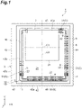
FIG. 1 is a plan view of a photodetector of an embodiment. -
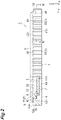
FIG. 2 is a side view of the photodetector illustrated inFIG. 1 . -
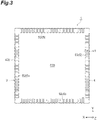
FIG. 3 is a bottom view of the photodetector illustrated inFIG. 1 . -
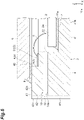
FIG. 4 is a cross-sectional view along line IV-IV illustrated inFIG. 2 . -
FIG. 5 is a cross-sectional view along line V-V illustrated inFIG. 4 . -
FIG. 6 is a cross-sectional view of the photodetector of a modification example. -
FIG. 7 is a cross-sectional view of the photodetector of another modification example. - Hereinafter, an embodiment of the present disclosure will be described in detail with reference to the drawings. In each of the diagrams, the same reference signs are applied to parts which are the same or corresponding, and duplicate description thereof will be omitted.
- As illustrated in
FIGS. 1 ,2 , and3 , aphotodetector 1 includes alight receiving element 2 and apackage 3 accommodating thelight receiving element 2. Thepackage 3 has anaccommodation member 4, a plurality ofwirings 5, and alight transmitting member 6. Hereinafter, an incident direction of light with respect to thephotodetector 1 will be referred to as a Z direction, a direction perpendicular to the Z direction will be referred to as an X direction, and a direction perpendicular to both the Z direction and the X direction will be referred to as a Y direction. - The
light receiving element 2 is a rear incident-type solid state imaging element (for example, a CMOS image sensor). For example, thelight receiving element 2 exhibits a rectangular plate shape having each of the X direction and the Y direction as an extending direction of each side and having the Z direction as a thickness direction thereof. As an example, a length of each side of thelight receiving element 2 is approximately around ten mm, and a thickness of thelight receiving element 2 is approximately several hundred µm. - The
light receiving element 2 is provided with alight receiving portion 21 and a plurality ofterminals 22. For example, thelight receiving portion 21 exhibits a rectangular shape having each of the X direction and the Y direction as an extending direction of each side. As an example, a length of each side of thelight receiving portion 21 is approximately several mm to around ten mm. In thelight receiving element 2, thelight receiving portion 21 is offset to one side in the X direction (the left side inFIG. 1 ) and one side in the Y direction (the upper side inFIG. 1 ). Regions other than thelight receiving portion 21 in thelight receiving element 2 is provided with circuits such as a CMOS reading circuit, a vertical scanning circuit, and a horizontal scanning circuit (not illustrated). The plurality ofterminals 22 are disposed along an outer edge of asurface 2a of thelight receiving element 2. Each of theterminals 22 is buried on thesurface 2a in an exposed state on thesurface 2a. Each of theterminals 22 is electrically connected to the circuits of thelight receiving element 2. - The
accommodation member 4 includes abottom wall 41 and aside wall 42 and is formed of a ceramic. Thebottom wall 41 and theside wall 42 are integrally formed by sintering of a laminate. Thebottom wall 41 is a part between a flat surface including aplacement surface 41a (which will be described below) and anouter surface 41b in theaccommodation member 4. For example, thebottom wall 41 exhibits a rectangular plate shape having each of the X direction and the Y direction as an extending direction of each side and having the Z direction as a thickness direction thereof. As an example, a length of each side of thebottom wall 41 is approximately around ten mm, and a thickness of the bottom wall 41 (that is, a distance between a flat surface including theplacement surface 41a and theouter surface 41b) is approximately several hundred µm. Theside wall 42 defines anopening 40 facing thebottom wall 41 in the Z direction. For example, theside wall 42 exhibits a rectangular frame shape extending along an outer edge of thebottom wall 41. As an example, a height of theside wall 42 is approximately several hundred µm, and a thickness of theside wall 42 is approximately several mm. - The
side wall 42 is constituted of a plurality ofside wall portions side wall portion 43 is positioned on one side in the X direction (the left side inFIG. 1 ). Theside wall portion 44 is positioned on the other side in the X direction (the right side inFIG. 1 ). Theside wall portion 45 is positioned on one side in the Y direction (the upper side inFIG. 1 ). Theside wall portion 46 is positioned on the other side in the Y direction (the lower side inFIG. 1 ). - The
placement surface 41a is formed in thebottom wall 41. Theplacement surface 41a is an inner surface of thebottom wall 41 on theopening 40 side. Thelight receiving element 2 is attached to theplacement surface 41a by anadhesive member 7 in a state in which thesurface 2a of thelight receiving element 2 faces theopening 40 side. Thesurface 2a of thelight receiving element 2 on theopening 40 side is positioned between theplacement surface 41a and anend surface 42a of the side wall 42 (an end surface of theside wall 42 on a side opposite to the bottom wall 41) in the Z direction. A gap is formed between thelight receiving element 2 and theside wall 42. As an example, a width of the gap is approximately several hundred µm. - A
pad surface 42b is formed in theside wall 42. Thepad surface 42b extends along an inner edge of theside wall 42. Thepad surface 42b is positioned on theopening 40 side with respect to theplacement surface 41a of thebottom wall 41 and positioned on thebottom wall 41 side with respect to theend surface 42a of theside wall 42 in the Z direction. Namely, thepad surface 42b is positioned between theplacement surface 41a and theend surface 42a in the Z direction. A height difference between thesurface 2a of thelight receiving element 2 and thepad surface 42b (that is, a distance between thesurface 2a and thepad surface 42b in the Z direction) is smaller than the thickness of thelight receiving element 2. In the present embodiment, the height difference between thesurface 2a of thelight receiving element 2 and thepad surface 42b is substantially zero. The width of the gap formed between thelight receiving element 2 and theside wall 42 is smaller than a width of thepad surface 42b (a width of thepad surface 42b in a direction perpendicular to the extending direction of thepad surface 42b extending along the inner edge of the side wall 42). - The plurality of
wirings 5 are provided in theaccommodation member 4. Each of thewirings 5 reaches theouter surface 41b of thebottom wall 41 from thepad surface 42b via the inside of theside wall 42 and anouter surface 42c of theside wall 42. A material of each of thewirings 5 is a metal, for example. Each of thewirings 5 includespads connection portion 53. Thepad 51 is disposed on thepad surface 42b. Thepad 52 is disposed along an outer edge of theouter surface 41b of thebottom wall 41. Theconnection portion 53 extends in the Z direction on theouter surface 42c of theside wall 42. For example, theaccommodation member 4 and the plurality ofwirings 5 are integrally formed by baking a laminate of green sheets on which a wiring pattern is formed. The terminal 22 and thepad 51 for thewiring 5 corresponding to each other in thelight receiving element 2 are electrically connected to each other by awire 8. - The
light transmitting member 6 is attached to theside wall 42 such that theopening 40 is covered. Thelight transmitting member 6 is attached to theend surface 42a of theside wall 42 by anadhesive member 9. The material of thelight transmitting member 6 is a glass, for example. For example, thelight transmitting member 6 exhibits a rectangular plate shape having each of the X direction and the Y direction as an extending direction of each side and having the Z direction as a thickness direction thereof. As an example, a length of each side of thelight transmitting member 6 is approximately around ten mm, and a thickness of thelight transmitting member 6 is approximately several hundred µm. Thelight transmitting member 6 is separated from thelight receiving element 2 and a plurality ofwires 8. - As described above, the
light receiving portion 21 is offset to one side in the X direction (the left side inFIG. 1 ) in thelight receiving element 2. However, when viewed in the Z direction (in a direction in which thebottom wall 41 and theopening 40 face each other), a center position C1 of thelight receiving portion 21 coincides with a center position C2 of thepackage 3 in the X direction (predetermined direction). This is realized by causing a thickness of theside wall portion 43 positioned on one side in the X direction (the left side inFIG. 1 ) to be larger than a thickness of theside wall portion 44 positioned on the other side in the X direction (the right side inFIG. 1 ). The center position C1 of thelight receiving portion 21 is also a centroidal position of thelight receiving portion 21 when viewed in the Z direction, and the center position C2 of thepackage 3 is also a centroidal position of thepackage 3 when viewed in the Z direction. - A through
hole 10 is formed at acorner portion 47 of theside wall 42. Thecorner portion 47 is a corner portion of theside wall 42 when viewed in the Z direction and is a corner portion formed by theside wall portion 43 and theside wall portion 46. Only one throughhole 10 is formed in theside wall 42. The throughhole 10 allows communication between the inside of the package 3 (that is, an inner space of the package 3) and the outside of the package 3 (that is, an outer space of the package 3). Aninner end portion 11 of the throughhole 10 is positioned on aninner surface 42d of theside wall 42, and anouter end portion 12 of the throughhole 10 is positioned on theouter surface 42c of theside wall 42. When viewed in the Z direction, theinner end portion 11 of the throughhole 10 is positioned on a side opposite to the center position C1 of thelight receiving portion 21 with respect to the center position C2 of thepackage 3 in the Y direction (predetermined direction). - As illustrated in
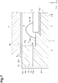
FIGS. 4 and5 , theinner end portion 11 of the throughhole 10 is positioned on theopening 40 side with respect to thesurface 2a of thelight receiving element 2 in the Z direction. In the present embodiment, the entirety of the throughhole 10 including theinner end portion 11 and theouter end portion 12 of the throughhole 10 is positioned on theopening 40 side through a wire thepad surface 42b in the Z direction. The cross-sectional shape of the throughhole 10 is a rectangular shape, for example. As an example, each of the width and the height of the throughhole 10 is approximately several hundred µm, and the width of the throughhole 10 is larger than the height of the throughhole 10. - The
inner end portion 11 of the throughhole 10 is positioned on at aninside corner portion 47a on the inward side in thecorner portion 47. Theinside corner portion 47a is an inside corner portion of theinner surface 42d of theside wall 42 when viewed in the Z direction. Theouter end portion 12 of the throughhole 10 is positioned on an outer surface of theside wall portion 43. Theside wall portion 43 is a side wall portion having the largest thickness of the plurality ofside wall portions side wall 42. The throughhole 10 has a plurality ofbent portions 13. Aninternal surface 10a of the throughhole 10 exhibits a rounded shape (that is, a round-chamfered shape) in each of thebent portions 13 when viewed in the Z direction. - A plurality of
groove portions 48 and one groove portion (recess portion) 49 are formed on theouter surface 42c of theside wall 42. Each of thegroove portions groove portions groove portions connection portion 53 of thewiring 5 is disposed in each of thegroove portions 48. Theouter end portion 12 of the throughhole 10 is positioned in thegroove portion 49. Theconnection portion 53 of thewiring 5 is not disposed in thegroove portion 49. A distance D1 between theconnection portion 53 closest to theouter end portion 12 of the throughhole 10 of a plurality ofconnection portions 53 and theouter end portion 12 of the throughhole 10 is longer than a distance D2 between theconnection portion 53 closest to theouter end portion 12 of the throughhole 10 of the plurality ofconnection portions 53 and theconnection portion 53 second closest to theouter end portion 12 of the throughhole 10 of the plurality ofconnection portions 53. - As described above, in the
photodetector 1, in theaccommodation member 4 formed of a ceramic, thepad surface 42b on which thepad 51 of each of thewirings 5 is disposed is positioned on theopening 40 side with respect to theplacement surface 41a to which thelight receiving element 2 is attached by theadhesive member 7. Accordingly, theadhesive member 7 is unlikely to reach thepad surface 42b. Therefore, the terminal 22 and thepad 51 for thewiring 5 corresponding to each other in thelight receiving element 2 are reliably connected to each other by thewire 8. Moreover, in thephotodetector 1, in theaccommodation member 4 formed of a ceramic, theinner end portion 11 of the throughhole 10 formed in theside wall 42 is positioned on theopening 40 side with respect to thesurface 2a of thelight receiving element 2. Accordingly, theinner end portion 11 of the throughhole 10 is unlikely to be blocked by theadhesive member 7. Therefore, ventilation between the inside and the outside of thepackage 3 is secured, and occurrence of dew condensation (for example, dew condensation occurring due to a temperature difference caused by a reflow step when thephotodetector 1 is mounted) inside thepackage 3 is reliably prevented. Hence, according to thephotodetector 1, electrical connection between the plurality ofwirings 5 provided in thepackage 3 and thelight receiving element 2 accommodated inside thepackage 3 can be reliably performed, and occurrence of dew condensation inside thepackage 3 can be reliably prevented. - In the
photodetector 1, theinner end portion 11 of the throughhole 10 is positioned on theopening 40 side with respect to thesurface 2a of thelight receiving element 2. Therefore, air can be smoothly discharged from the inside of thepackage 3 to the outside of thepackage 3. In addition, since theinner end portion 11 of the throughhole 10 is positioned on theopening 40 side with respect to thesurface 2a of thelight receiving element 2, even if gas is generated from theadhesive member 9, the gas can be efficiently discharged from the inside of thepackage 3 to the outside of thepackage 3. Moreover, since theinner end portion 11 of the throughhole 10 is positioned on theopening 40 side with respect to thesurface 2a of thelight receiving element 2 and theinner end portion 11 of the throughhole 10 is unlikely to be blocked by theadhesive member 7, the distance between thelight receiving element 2 and theside wall 42 can be reduced, and thus miniaturization of thephotodetector 1 can be achieved. In addition, if thelight receiving element 2 is a rear incident-type solid state imaging element and a resin adhesive member is used between a support substrate and a device layer, dew condensation is likely to occur inside thepackage 3 due to hygroscopic properties of the resin adhesive member. Therefore, it is particularly effective to provide the throughhole 10 in theaccommodation member 4. - In the
photodetector 1, theinner end portion 11 of the throughhole 10 is positioned on theopening 40 side with respect to thepad surface 42b. Accordingly, even if a foreign substance intrudes into thepackage 3 through the throughhole 10, the foreign substance can be easily captured on thepad surface 42b. Moreover, thelight receiving portion 21 is separated from theinner end portion 11 of the throughhole 10 by an amount corresponding to a thickness of thepad surface 42b therebetween. Hence, even if a foreign substance intrudes into thepackage 3 through the throughhole 10, arrival of the foreign substance at thelight receiving portion 21 can be curbed. - In the
photodetector 1, theinner end portion 11 of the throughhole 10 is positioned on theopening 40 side with respect to thepad surface 42b. Therefore, the degree of freedom in laying the plurality ofwirings 5 can be secured at a part on thebottom wall 41 side of thepad surface 42b in theside wall 42. - In the
photodetector 1, the throughhole 10 has the plurality ofbent portions 13. Accordingly, intrusion of a foreign substance into thepackage 3 through the throughhole 10 can be curbed. - In the
photodetector 1, theinternal surface 10a of the throughhole 10 exhibits a rounded shape in each of thebent portions 13. Accordingly, theaccommodation member 4 is unlikely to break at each of thebent portions 13. Therefore, intrusion of a foreign substance into thepackage 3 caused by such breakage can be curbed. - In the
photodetector 1, the throughhole 10 is a single hole. Accordingly, compared to when there are a plurality of throughholes 10, intrusion of a foreign substance into thepackage 3 through the throughhole 10 can be curbed. - In the
photodetector 1, theinner end portion 11 of the throughhole 10 is positioned at theinside corner portion 47a on theinner surface 42d of theside wall 42. Accordingly, smooth ventilation between the inside and the outside of thepackage 3 can be achieved. - In the
photodetector 1, the throughhole 10 is formed at thecorner portion 47 in theside wall 42. Accordingly, a length of the throughhole 10 can be increased, and intrusion of a foreign substance into thepackage 3 through the throughhole 10 can be curbed. - In the
photodetector 1, theouter end portion 12 of the throughhole 10 is positioned on the outer surface of theside wall portion 43 having the largest thickness of the plurality ofside wall portions hole 10 can be increased, and intrusion of a foreign substance into thepackage 3 through the throughhole 10 can be curbed. - In the
photodetector 1, theouter end portion 12 of the throughhole 10 is positioned in thegroove portion 49 formed on theouter surface 42c of theside wall 42. Accordingly, intrusion of a foreign substance into theouter end portion 12 of the throughhole 10 can be curbed. - In the
photodetector 1, the distance D1 between theconnection portion 53 closest to theouter end portion 12 of the throughhole 10 of the plurality ofconnection portions 53 and theouter end portion 12 of the throughhole 10 is longer than the distance D2 between theconnection portion 53 closest to theouter end portion 12 of the throughhole 10 of the plurality ofconnection portions 53 and theconnection portion 53 second closest to theouter end portion 12 of the throughhole 10 of the plurality ofconnection portions 53. Accordingly, blocking of theouter end portion 12 of the throughhole 10 by a reflow material which has melted when thephotodetector 1 is mounted can be curbed. - In the
photodetector 1, when viewed in the Z direction, the center position C1 of thelight receiving portion 21 coincides with the center position C2 of thepackage 3 in the X direction. Accordingly, when thephotodetector 1 is mounted, positioning of thelight receiving portion 21 can be performed based on thepackage 3 in the X direction. - In the
photodetector 1, theinner end portion 11 of the throughhole 10 is positioned on a side opposite to the center position C1 of thelight receiving portion 21 with respect to the center position C2 of thepackage 3 in the Y direction when viewed in the Z direction. Accordingly, thelight receiving portion 21 is separated from theinner end portion 11 of the throughhole 10 in the Y direction. Therefore, even if a foreign substance intrudes into thepackage 3 through the throughhole 10, arrival of the foreign substance at thelight receiving portion 21 can be curbed. - In the
photodetector 1, a gap is formed between thelight receiving element 2 and theside wall 42. Accordingly, even if a foreign substance intrudes into thepackage 3 through the throughhole 10, the foreign substance can be easily captured by the gap between thelight receiving element 2 and theside wall 42. Therefore, arrival of a foreign substance at thelight receiving portion 21 can be curbed. In thephotodetector 1, the width of the gap formed between thelight receiving element 2 and theside wall 42 is smaller than the width of thepad surface 42b. Therefore, miniaturization of the entirety of thepackage 3 can be achieved. At this time, even if the width of the gap is reduced, theinner end portion 11 of the throughhole 10 is positioned on theopening 40 side of thesurface 2a of thelight receiving element 2. Therefore, theinner end portion 11 of the throughhole 10 is unlikely to be blocked by theadhesive member 7. - In the
photodetector 1, the height difference between thesurface 2a of thelight receiving element 2 and thepad surface 42b is smaller than the thickness of thelight receiving element 2. Accordingly, connection of thewire 8 to theterminal 22 of thelight receiving element 2 and thepad 51 of thewiring 5 corresponding to each other can be easily performed. - The present disclosure is not limited to the embodiment described above. For example, regarding the position of the
inner end portion 11 of the throughhole 10, at least a portion of theinner end portion 11 of the throughhole 10 need only be positioned on theopening 40 side of thepad surface 42b in the Z direction. If the entirety of theinner end portion 11 of the throughhole 10 is positioned on theopening 40 side of theplacement surface 41a in the Z direction, blocking of theinner end portion 11 of the throughhole 10 by theadhesive member 7 can be curbed. - In addition, at least a portion of the
inner end portion 11 of the throughhole 10 need only be positioned on theopening 40 side of thesurface 2a of thelight receiving element 2 in the Z direction. In such a case, as illustrated inFIG. 6 , thepad surface 42b may be positioned on theopening 40 side with respect to thesurface 2a of thelight receiving element 2 in the Z direction, and at least a portion of theinner end portion 11 of the throughhole 10 may be positioned between thepad surface 42b and thesurface 2a of thelight receiving element 2 in the Z direction. In addition, as illustrated inFIG. 7 , thesurface 2a of thelight receiving element 2 may be positioned on theopening 40 side with respect to thepad surface 42b in the Z direction, and at least a portion of theinner end portion 11 of the throughhole 10 may be positioned on theopening 40 side with respect to thepad surface 42b and thesurface 2a of thelight receiving element 2 in the Z direction. - In addition, the shape of the through
hole 10 and the number thereof are not limited to those described above as long as the throughhole 10 is formed in theside wall 42. For example, the throughhole 10 need only have at least onebent portion 13. In addition, the throughhole 10 may not have thebent portions 13. In addition, theouter end portion 12 of the throughhole 10 may be positioned in a recess portion exhibiting a shape other than those of thegroove portions 48. In addition, a plurality of throughholes 10 may be formed in theside wall 42. - In addition, the
light receiving element 2 may be a front incident-type solid state imaging element. In addition, thelight receiving element 2 may be a PD array or the like. In addition, thepad surface 42b need only be formed in thebottom wall 41 or theside wall 42. However, from a viewpoint of miniaturizing the entirety of thepackage 3, it is more preferable to form thepad surface 42b in theside wall 42 than to form thepad surface 42b in thebottom wall 41. - 1: Photodetector, 2: Light receiving element, 2a: Surface, 21: Light receiving portion, 22: Terminal, 3: Package, 4: Accommodation member, 40: Opening, 41: Bottom wall, 41a: Placement surface, 42: Side wall, 42b: Pad surface, 42c: Outer surface, 42d: Inner surface, 43, 44, 45, 46: Side wall portion, 47: Corner portion, 47a: Inside corner portion, 49: Groove portion (recess portion), 5: Wiring, 51: Pad, 53: Connection portion, 6: Light transmitting member, 7: Adhesive member, 8: Wire, 10: Through hole, 10a: Internal surface, 11: Inner end portion, 12: Outer end portion, 13: Bent portion.
Claims (14)
- A photodetector comprising:a light receiving element provided with a light receiving portion and a terminal; anda package accommodating the light receiving element,wherein the package hasan accommodation member including a bottom wall and a side wall defining an opening facing the bottom wall, the accommodation member formed of a ceramic,a wiring including a pad connected to the terminal by a wire, the wiring provided in the accommodation member, anda light transmitting member attached to the side wall such that the opening is covered,wherein the bottom wall has a placement surface to which the light receiving element is attached by an adhesive member,wherein the bottom wall or the side wall has a pad surface on which the pad is disposed, the pad surface positioned on the opening side with respect to the placement surface,wherein the side wall has a through hole allowing communication between the inside of the package and the outside of the package, andwherein at least a portion of an inner end portion of the through hole is positioned on the opening side with respect to a surface of the light receiving element on the opening side.
- The photodetector according to claim 1,
wherein at least a portion of the inner end portion of the through hole is positioned on the opening side with respect to the pad surface. - The photodetector according to claim 1 or 2,
wherein the through hole has a bent portion. - The photodetector according to claim 3,
wherein an internal surface of the through hole exhibits a rounded shape at the bent portion. - The photodetector according to any one of claims 1 to 4,
wherein the through hole is a single hole. - The photodetector according to any one of claims 1 to 5,wherein an inner surface of the side wall has an inside corner portion when viewed in a direction in which the bottom wall and the opening face each other, andwherein the inner end portion of the through hole is positioned at the inside corner portion.
- The photodetector according to any one of claims 1 to 6,wherein the side wall has a corner portion when viewed in a direction in which the bottom wall and the opening face each other, andwherein the through hole is formed at the corner portion.
- The photodetector according to any one of claims 1 to 7,wherein the side wall includes a plurality of side wall portions, andwherein an outer end portion of the through hole is positioned on an outer surface of a side wall portion having the largest thickness of the plurality of side wall portions.
- The photodetector according to any one of claims 1 to 8,wherein a recess portion is formed on an outer surface of the side wall, andwherein an outer end portion of the through hole is positioned in the recess portion.
- The photodetector according to any one of claims 1 to 9,wherein the wiring includes a plurality of connection portions extending in a direction in which the bottom wall and the opening face each other on an outer surface of the side wall, andwherein a distance between a connection portion closest to an outer end portion of the through hole of the plurality of connection portions and the outer end portion of the through hole is longer than a distance between the connection portion closest to the outer end portion of the through hole of the plurality of connection portions and a connection portion second closest to the outer end portion of the through hole of the plurality of connection portions.
- The photodetector according to any one of claims 1 to 10,
wherein a center position of the light receiving portion coincides with a center position of the package in at least a predetermined direction when viewed in a direction in which the bottom wall and the opening face each other. - The photodetector according to any one of claims 1 to 11,
wherein the inner end portion of the through hole is positioned on a side opposite to the center position of the light receiving portion with respect to the center position of the package in at least a predetermined direction when viewed in a direction in which the bottom wall and the opening face each other. - The photodetector according to any one of claims 1 to 12,
wherein a gap is formed between the light receiving element and the side wall. - The photodetector according to any one of claims 1 to 13,
wherein a height difference between the surface of the light receiving element on the opening side and the pad surface is smaller than a thickness of the light receiving element.
Applications Claiming Priority (2)
| Application Number | Priority Date | Filing Date | Title |
|---|---|---|---|
| JP2019179193A JP6839248B1 (en) | 2019-09-30 | 2019-09-30 | Photodetector |
| PCT/JP2020/032645 WO2021065272A1 (en) | 2019-09-30 | 2020-08-28 | Photodetector |
Publications (2)
| Publication Number | Publication Date |
|---|---|
| EP4040476A1 true EP4040476A1 (en) | 2022-08-10 |
| EP4040476A4 EP4040476A4 (en) | 2023-10-04 |
Family
ID=74673668
Family Applications (1)
| Application Number | Title | Priority Date | Filing Date |
|---|---|---|---|
| EP20871226.5A Withdrawn EP4040476A4 (en) | 2019-09-30 | 2020-08-28 | Photodetector |
Country Status (5)
| Country | Link |
|---|---|
| EP (1) | EP4040476A4 (en) |
| JP (1) | JP6839248B1 (en) |
| CN (1) | CN114450796B (en) |
| TW (1) | TWI855161B (en) |
| WO (1) | WO2021065272A1 (en) |
Family Cites Families (19)
| Publication number | Priority date | Publication date | Assignee | Title |
|---|---|---|---|---|
| FR2824955B1 (en) * | 2001-05-18 | 2004-07-09 | St Microelectronics Sa | SHIELDED OPTICAL SEMICONDUCTOR PACKAGE |
| JP4351012B2 (en) * | 2003-09-25 | 2009-10-28 | 浜松ホトニクス株式会社 | Semiconductor device |
| JP4554492B2 (en) * | 2005-11-01 | 2010-09-29 | シャープ株式会社 | Manufacturing method of semiconductor package |
| JP4466552B2 (en) * | 2005-12-09 | 2010-05-26 | ソニー株式会社 | Method for manufacturing solid-state imaging device |
| JP5193492B2 (en) * | 2007-04-25 | 2013-05-08 | 浜松ホトニクス株式会社 | Optical semiconductor device |
| EP2172970A4 (en) * | 2007-07-19 | 2012-04-04 | Fujikura Ltd | Semiconductor package and its manufacturing method |
| JP2009081303A (en) * | 2007-09-26 | 2009-04-16 | Panasonic Corp | Semiconductor device and manufacturing method thereof |
| JP2009289830A (en) * | 2008-05-27 | 2009-12-10 | Mitsui Chemicals Inc | Package for semiconductor element mounting |
| JP5136215B2 (en) * | 2008-05-29 | 2013-02-06 | 住友ベークライト株式会社 | Semiconductor device |
| JP2010177351A (en) * | 2009-01-28 | 2010-08-12 | Sharp Corp | Solid-state imaging device and electronic apparatus including the same |
| US8912453B2 (en) * | 2009-12-18 | 2014-12-16 | Mitsubishi Electric Corporation | Electronic component package |
| US9275949B2 (en) * | 2011-06-01 | 2016-03-01 | Canon Kabushiki Kaisha | Semiconductor device |
| US8884413B2 (en) * | 2012-08-31 | 2014-11-11 | Freescale Semiconductor, Inc. | Leadframes, air-cavity packages, and electronic devices with offset vent holes, and methods of their manufacture |
| JP5925711B2 (en) * | 2013-02-20 | 2016-05-25 | 浜松ホトニクス株式会社 | Detector, PET apparatus and X-ray CT apparatus |
| US10184832B2 (en) * | 2013-10-31 | 2019-01-22 | Hamamatsu Photonics K.K. | Light-detecting device |
| JP2015216142A (en) | 2014-05-07 | 2015-12-03 | キヤノン株式会社 | Container manufacturing method, container member, container, solid-state imaging device manufacturing method, and solid-state imaging device |
| JP2017041615A (en) * | 2015-08-21 | 2017-02-23 | 株式会社フジクラ | Optical element module and manufacturing method of the same |
| JP6483854B2 (en) * | 2016-05-20 | 2019-03-13 | 京セラ株式会社 | Electronic device mounting substrate and electronic device |
| JP7025153B2 (en) * | 2017-09-08 | 2022-02-24 | エムテックスマツムラ株式会社 | Hollow package container, semiconductor device package and its manufacturing method |
-
2019
- 2019-09-30 JP JP2019179193A patent/JP6839248B1/en active Active
-
2020
- 2020-08-28 WO PCT/JP2020/032645 patent/WO2021065272A1/en not_active Ceased
- 2020-08-28 EP EP20871226.5A patent/EP4040476A4/en not_active Withdrawn
- 2020-08-28 CN CN202080068182.XA patent/CN114450796B/en active Active
- 2020-09-21 TW TW109132524A patent/TWI855161B/en active
Also Published As
| Publication number | Publication date |
|---|---|
| TWI855161B (en) | 2024-09-11 |
| JP6839248B1 (en) | 2021-03-03 |
| US20220344520A1 (en) | 2022-10-27 |
| CN114450796A (en) | 2022-05-06 |
| TW202118078A (en) | 2021-05-01 |
| WO2021065272A1 (en) | 2021-04-08 |
| JP2021057454A (en) | 2021-04-08 |
| EP4040476A4 (en) | 2023-10-04 |
| CN114450796B (en) | 2026-03-17 |
Similar Documents
| Publication | Publication Date | Title |
|---|---|---|
| US7682159B2 (en) | Electrical connector and camera device having the same | |
| US8773867B2 (en) | Camera module for shielding EMI | |
| CN100490162C (en) | Solid-state imaging device and method for producing the same | |
| JP5465288B2 (en) | Infrared sensor | |
| JPWO2013118501A1 (en) | Imaging unit and imaging apparatus | |
| US8053685B2 (en) | Metal wiring plate | |
| JP2006210205A (en) | Socket for module | |
| JP4646960B2 (en) | Package for storing solid-state imaging device and imaging apparatus | |
| EP1705479B1 (en) | Gas sensor | |
| KR100696429B1 (en) | Arrangement of Camera Module in Portable Device | |
| JPH11252416A (en) | Mounting method of solid-state image sensor | |
| JP4652149B2 (en) | The camera module | |
| US12622092B2 (en) | Photodetector | |
| EP4040476A1 (en) | Photodetector | |
| KR20220001966A (en) | Camera module | |
| KR102054852B1 (en) | Camera for mounting on vehicle | |
| TWI758549B (en) | Substrate laminate, and imaging device | |
| JP4622995B2 (en) | Electronic control unit | |
| CN205453015U (en) | Electrical connection box | |
| CN211791698U (en) | Camera assembly and electronic product | |
| JP4157109B2 (en) | Protective cover mounting structure | |
| CN109278643B (en) | Camera equipment for observing the driver of the vehicle | |
| CN101355219B (en) | Connector | |
| JP2005129720A (en) | Solid-state imaging device and manufacturing method thereof | |
| US12080813B2 (en) | Optical semiconductor device |
Legal Events
| Date | Code | Title | Description |
|---|---|---|---|
| STAA | Information on the status of an ep patent application or granted ep patent |
Free format text: STATUS: THE INTERNATIONAL PUBLICATION HAS BEEN MADE |
|
| PUAI | Public reference made under article 153(3) epc to a published international application that has entered the european phase |
Free format text: ORIGINAL CODE: 0009012 |
|
| STAA | Information on the status of an ep patent application or granted ep patent |
Free format text: STATUS: REQUEST FOR EXAMINATION WAS MADE |
|
| 17P | Request for examination filed |
Effective date: 20220331 |
|
| AK | Designated contracting states |
Kind code of ref document: A1 Designated state(s): AL AT BE BG CH CY CZ DE DK EE ES FI FR GB GR HR HU IE IS IT LI LT LU LV MC MK MT NL NO PL PT RO RS SE SI SK SM TR |
|
| DAV | Request for validation of the european patent (deleted) | ||
| DAX | Request for extension of the european patent (deleted) | ||
| REG | Reference to a national code |
Ref country code: DE Ref legal event code: R079 Free format text: PREVIOUS MAIN CLASS: H01L0023020000 Ipc: H01L0027146000 |
|
| A4 | Supplementary search report drawn up and despatched |
Effective date: 20230905 |
|
| RIC1 | Information provided on ipc code assigned before grant |
Ipc: H01L 23/02 20060101ALI20230830BHEP Ipc: H01L 31/0203 20140101ALI20230830BHEP Ipc: H01L 27/146 20060101AFI20230830BHEP |
|
| STAA | Information on the status of an ep patent application or granted ep patent |
Free format text: STATUS: THE APPLICATION HAS BEEN WITHDRAWN |
|
| 18W | Application withdrawn |
Effective date: 20260312 |