EP4040456A1 - Film capacitor element - Google Patents
Film capacitor element Download PDFInfo
- Publication number
- EP4040456A1 EP4040456A1 EP20870793.5A EP20870793A EP4040456A1 EP 4040456 A1 EP4040456 A1 EP 4040456A1 EP 20870793 A EP20870793 A EP 20870793A EP 4040456 A1 EP4040456 A1 EP 4040456A1
- Authority
- EP
- European Patent Office
- Prior art keywords
- metal strips
- film
- dielectric films
- end faces
- film stack
- Prior art date
- Legal status (The legal status is an assumption and is not a legal conclusion. Google has not performed a legal analysis and makes no representation as to the accuracy of the status listed.)
- Withdrawn
Links
Images



Classifications
-
- H—ELECTRICITY
- H01—ELECTRIC ELEMENTS
- H01G—CAPACITORS; CAPACITORS, RECTIFIERS, DETECTORS, SWITCHING DEVICES, LIGHT-SENSITIVE OR TEMPERATURE-SENSITIVE DEVICES OF THE ELECTROLYTIC TYPE
- H01G4/00—Fixed capacitors; Processes of their manufacture
- H01G4/33—Thin- or thick-film capacitors (thin- or thick-film circuits; capacitors without a potential-jump or surface barrier specially adapted for integrated circuits, details thereof, multistep manufacturing processes therefor)
-
- H—ELECTRICITY
- H01—ELECTRIC ELEMENTS
- H01G—CAPACITORS; CAPACITORS, RECTIFIERS, DETECTORS, SWITCHING DEVICES, LIGHT-SENSITIVE OR TEMPERATURE-SENSITIVE DEVICES OF THE ELECTROLYTIC TYPE
- H01G4/00—Fixed capacitors; Processes of their manufacture
- H01G4/32—Wound capacitors
-
- H—ELECTRICITY
- H01—ELECTRIC ELEMENTS
- H01G—CAPACITORS; CAPACITORS, RECTIFIERS, DETECTORS, SWITCHING DEVICES, LIGHT-SENSITIVE OR TEMPERATURE-SENSITIVE DEVICES OF THE ELECTROLYTIC TYPE
- H01G4/00—Fixed capacitors; Processes of their manufacture
- H01G4/002—Details
- H01G4/228—Terminals
- H01G4/232—Terminals electrically connecting two or more layers of a stacked or rolled capacitor
-
- H—ELECTRICITY
- H01—ELECTRIC ELEMENTS
- H01G—CAPACITORS; CAPACITORS, RECTIFIERS, DETECTORS, SWITCHING DEVICES, LIGHT-SENSITIVE OR TEMPERATURE-SENSITIVE DEVICES OF THE ELECTROLYTIC TYPE
- H01G4/00—Fixed capacitors; Processes of their manufacture
- H01G4/002—Details
- H01G4/005—Electrodes
-
- H—ELECTRICITY
- H01—ELECTRIC ELEMENTS
- H01G—CAPACITORS; CAPACITORS, RECTIFIERS, DETECTORS, SWITCHING DEVICES, LIGHT-SENSITIVE OR TEMPERATURE-SENSITIVE DEVICES OF THE ELECTROLYTIC TYPE
- H01G4/00—Fixed capacitors; Processes of their manufacture
- H01G4/002—Details
- H01G4/005—Electrodes
- H01G4/012—Form of non-self-supporting electrodes
-
- H—ELECTRICITY
- H01—ELECTRIC ELEMENTS
- H01G—CAPACITORS; CAPACITORS, RECTIFIERS, DETECTORS, SWITCHING DEVICES, LIGHT-SENSITIVE OR TEMPERATURE-SENSITIVE DEVICES OF THE ELECTROLYTIC TYPE
- H01G4/00—Fixed capacitors; Processes of their manufacture
- H01G4/002—Details
- H01G4/005—Electrodes
- H01G4/015—Special provisions for self-healing
-
- H—ELECTRICITY
- H01—ELECTRIC ELEMENTS
- H01G—CAPACITORS; CAPACITORS, RECTIFIERS, DETECTORS, SWITCHING DEVICES, LIGHT-SENSITIVE OR TEMPERATURE-SENSITIVE DEVICES OF THE ELECTROLYTIC TYPE
- H01G4/00—Fixed capacitors; Processes of their manufacture
- H01G4/002—Details
- H01G4/018—Dielectrics
- H01G4/06—Solid dielectrics
-
- H—ELECTRICITY
- H01—ELECTRIC ELEMENTS
- H01G—CAPACITORS; CAPACITORS, RECTIFIERS, DETECTORS, SWITCHING DEVICES, LIGHT-SENSITIVE OR TEMPERATURE-SENSITIVE DEVICES OF THE ELECTROLYTIC TYPE
- H01G4/00—Fixed capacitors; Processes of their manufacture
- H01G4/002—Details
- H01G4/224—Housing; Encapsulation
-
- H—ELECTRICITY
- H01—ELECTRIC ELEMENTS
- H01G—CAPACITORS; CAPACITORS, RECTIFIERS, DETECTORS, SWITCHING DEVICES, LIGHT-SENSITIVE OR TEMPERATURE-SENSITIVE DEVICES OF THE ELECTROLYTIC TYPE
- H01G4/00—Fixed capacitors; Processes of their manufacture
- H01G4/30—Stacked capacitors
Definitions
- the present disclosure relates to a film capacitor device.
- Patent Literature 1 A known technique is described in, for example, Patent Literature 1.
- Patent Literature 1 Japanese Unexamined Patent Application Publication No. 2016-9775
- a film capacitor device includes a film stack being rectangular, external electrodes, insulation areas, and a conductor.
- the film stack includes a plurality of dielectric films being stacked.
- Each of the plurality of dielectric films includes a plurality of metal strips extending in a first direction on a surface of the dielectric film.
- Each of the plurality of dielectric films includes an insulation margin extending in the first direction as a groove between adjacent metal strips of the plurality of metal strips.
- Each of the plurality of dielectric films includes, at an edge of the surface of the dielectric film in the first direction, an edge insulation area continuously extending in a second direction perpendicular to the first direction.
- the plurality of dielectric films include adjacent dielectric films in 180° opposite orientations in the first direction on the surface and alternate dielectric films having the edge insulation areas overlapping in a plan view.
- the external electrodes are on a pair of end faces of the film stack in the first direction.
- the insulation areas electrically insulate metal strips of the plurality of metal strips at two ends of the film stack in the second direction from the external electrodes.
- the conductor continuously extends in a stacking direction on at least one of a pair of end faces of the film stack in the second direction.
- a film capacitor with the structure that forms the basis of a film capacitor device includes either a wound metalized film or metalized films stacked in one direction, which are metal layers to be an electrode, on the surface of a dielectric film of, for example, a polypropylene resin.
- a stacked film capacitor device is a rectangular block with an appropriate size (capacity) cut from a stack of metalized films.
- the stacked film capacitor includes external electrodes on its pair of side surfaces.
- the stacked film capacitor device with the structure that forms the basis of the film capacitor device according to one or more embodiments of the present disclosure includes the external electrodes (metal-sprayed electrodes) in areas not in contact with metal layers exposed at the ends, or specifically the cut surfaces of the stacked film capacitor device, instead of being arranged on the entire side surface. This structure reliably achieves insulation on the cut surfaces.
- the dielectric films being stacked may have slight misalignment during stacking.
- the metal layers not in contact with the external electrodes are floating.
- misalignment in stacking may cause the floating metal layers to overlap metal layers that are connected to the external electrodes in a plan view. This may cause a voltage to be applied to the floating metal layers through capacitive coupling.
- the floating metal layers are partially exposed at the cut surfaces. The application of voltage can thus cause electric discharge at the cut surfaces.
- a film capacitor device according to one or more embodiments will now be described with reference to the drawings.
- a film capacitor device 10 includes multiple dielectric films 1 and dielectric films 2 that are stacked alternately.
- Each of the dielectric films 1 and 2 includes, on its surface, multiple metal strips (films) 3 that continuously extend in a first direction (x-direction in the figure).
- the metal strips 3 serve as internal electrodes of the capacitor.
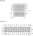
- the dielectric films 1 and 2 have the same structure as the structures shown in FIG. 1B and subsequent figures with the difference being their stacking orientations. To indicate the orientations in the stacked structure, the metal strips 3 are denoted with numerals 1A to IN or numerals 2Ato 2N in this order from an end of the dielectric film as shown in FIGs. 1A and 1D .
- the direction in which the metal strips 3 continuously extend parallel to one another is referred to as a first direction (x-direction), and the direction in which the metal strips 3 align parallel to one another (y-direction perpendicular to x-direction) is referred to as a second direction.
- the films are stacked on one another in a third direction (z-direction in the figures) perpendicular to the first and second directions.
- the metal strips 3 on the surface of each of the dielectric films 1 and 2 are formed by depositing metal on a base film (substrate) by vapor deposition.
- Each of the dielectric films 1 and 2 has surface portions as grooves each exposed between the metal strips 3 adjacent to each other in y-direction (hereafter, insulation margins S), which are also referred to as small margins.
- the metal strips 3 are thus separate and are electrically insulated from one another.
- Each of the insulation margins S (small margins) is continuous with an edge insulation area T at an end of the dielectric film in the first direction (x-direction).
- the edge insulation area T which is also referred to as a large margin, continuously extends in the second direction (y-direction).
- the dielectric films 1 and 2 included in the film capacitor device may be formed from an organic resin material such as polypropylene, polyethylene terephthalate, polyarylate, or cyclic olefin polymer.
- a film stack 4 includes the dielectric films 1 and 2 that are adjacent to each other in the vertical direction (z-direction) in the figure and are stacked alternately in 180° opposite orientations in x-direction. More specifically, the dielectric films 1 and 2 are stacked on one another to have their edge insulation areas T each located at an end (edge) of the corresponding dielectric film 1 or 2 to be alternately opposite to each other in x-direction.
- the film stack 4 includes, on its two end faces 4a in x-direction, metal electrodes that are formed by metal thermal spraying (hereafter, metal-sprayed electrodes).
- metal-sprayed electrodes metal electrodes that are formed by metal thermal spraying
- 5A indicates the metal-sprayed electrode at one end face 4a in x-direction
- 5B indicates the metal-sprayed electrode at the other end face 4a in x-direction. These electrodes are simply at different positions and have the same structure.
- the metal-sprayed electrodes 5A and 5B may be simply referred to as the metal-sprayed electrodes 5 without being distinguished from each other.
- the film capacitor device 10 includes the metal-sprayed electrodes 5A and 5B on the two end faces 4a in x-direction.
- the metal-sprayed electrodes 5A and 5B are not arranged on the entire end faces 4a.
- the film capacitor device 10 includes electrode-free areas 50 including no metal-sprayed electrodes 5 on the two ends of each end face 4a in y-direction.
- Each electrode-free area 50 has a predetermined width W and continuously extends in the stacking direction.
- the electrode-free areas 50 are insulation areas that electrically insulate the metal strips 3 located at the two ends of the film capacitor device in y-direction among the multiple metal strips 3 from the metal-sprayed electrodes 5.
- each electrode-free area 50 may be any dimension that can insulate one metal strip 3 located at each of the two ends in y-direction from the corresponding metal-sprayed electrode 5.
- the width W may thus be at least one time the pitch P between the insulation margins S. This allows the metal strip 3 at each of the two ends in y-direction to be insulated from the corresponding metal-sprayed electrode 5.
- the width W may be three times the pitch P or less. This structure reduces a decrease in capacitance resulting from insulation.
- the insulation areas cause the metal strips 3 at the two ends in y-direction to be floating electrodes, reliably achieving insulation on the two end faces 4b in y-direction.
- the two end faces 4b in y-direction are cut surfaces.
- Some floating electrodes may overlap the metal strips 3 connected to the metal-sprayed electrodes 5 in a plan view in the stacking direction due to misalignment in stacking. This may cause a voltage to be applied to the floating metal strips 3 through capacitive coupling. When multiple floating metal strips 3 aligned in the stacking direction are exposed at the end faces, the differences in potential between the metal strips 3 may cause electric discharge.
- the film capacitor device 10 includes a conductor 6 that continuously extends in the stacking direction on at least one of the two end faces 4b, which are the cut surfaces in y-direction.
- the conductor 6 serves as an equipotential area that electrically connects the floating metal strips 3 exposed at the cut surface to cause the exposed metal strips 3 to have the same potential. This reduces electric discharge at the cut surface.
- the conductor 6 may continuously extend in the stacking direction to electrically connect the exposed metal strips 3 aligned in the stacking direction at the end face 4b in y-direction as described above. In other words, the conductor 6 may extend to cover at least a part of the end face 4b, instead of covering the entire end face 4b. In the present embodiment, the conductor 6 is located over the entire end face 4b. Any metal strips 3 exposed at the end face 4b may thus be reliably connected and have the same potential.
- the conductors 6 may not be located on each of the two end faces 4b in y-direction, and may be on either of the two end faces 4b. In the present embodiment, the conductors 6 are on both the two end faces 4b in y-direction.
- the conductors 6 may be formed from any material using any method that allows electrical connection between the metal strips 3.
- Examples of the material for the conductors 6 include metal materials such as aluminum (Al), zinc (Zn), tin (Sn), silver (Ag), platinum (Pt), copper (Cu), nickel (Ni), iron (Fe), cobalt (Co), titanium (Ti), chromium (Cr), and lead (Pb).
- Metal powders including, for example, Cu, Ni, or Ag, or conductive adhesives containing carbon-based materials such as graphite may also be used.
- the conductors 6 may be formed from Al, Zn, or Sn by metal thermal spraying or sputtering.
- FIG. 2 is a plan view of a film capacitor device corresponding to FIG. 1B .
- the insulation areas electrically insulating the metal strips 3 at the two ends in y-direction from the metal-sprayed electrodes 5 in the second embodiment differ from the insulation areas in the first embodiment.
- the insulation areas in the present embodiment include recesses 11 between the metal-sprayed electrodes 5 and the film stack 4.
- the recesses 11 at the two ends of the film capacitor device 10 in y-direction separate the metal strips 3 from the metal-sprayed electrodes 5A and 5B.
- the film capacitor device 10 has four recesses 11 in total, which are two recesses 11 at one end of the film stack 4 in x-direction and two recesses 11 at the other end.
- Each recess 11 continuously extends in the stacking direction of the film (z-direction) between the metal-sprayed electrode 5A or 5B and the film stack 4 or in an area including the interface (boundary) between the metal-sprayed electrode 5A or 5B and the film stack 4.
- the recess 11 is open to an end face 4b of the film stack 4 in y-direction and has a depth D (y-direction) that is the same as the width W of each electrode-free area in the first embodiment.
- the recess 11 can insulate the metal strip 3 at one of the two ends in y-direction from the corresponding metal-sprayed electrode 5.
- the film capacitor device 10 when multiple floating metal strips 3 aligned in the stacking direction are exposed at the two end faces 4b in y-direction, the differences in potential between the metal strips 3 may cause electric discharge as in the first embodiment.
- the film capacitor device 10 according to the second embodiment also includes conductors 6 that continuously extend in the stacking direction on each of the two end faces 4b, which are the cut surfaces in y-direction. The conductors 6 can reduce electric discharge.
- FIG. 3 is a plan view of a film capacitor device corresponding to FIG. 1B .
- the conductors 6 on the two end faces 4b in y-direction in the third embodiment differ from the conductors 6 in the first embodiment.
- the conductors 6 in the present embodiment extend linearly in the stacking direction in a middle portion in x-direction, instead of being arranged on the entire end faces 4b.
- each end face 4b includes areas without any conductors 6 at its two ends in x-direction.
- electrode-free areas including no metal-sprayed electrodes 5 on the two end faces 4a in x-direction with a relatively small width W may cause a conductor 6 on the entire end face 4b to be closer to metal-sprayed electrodes 5 at the corners of the film stack 4. This may possibly cause a short circuit.
- the conductor 6 may simply extend in the middle portion in x-direction on the end face 4b in y-direction in the present embodiment. In the film capacitor device 10 according to the third embodiment as well, the conductor 6 can reduce electric discharge.
- FIG. 4 is a perspective view of a film capacitor device.
- the conductors 6 on the end faces 4b in y-direction in the fourth embodiment differ from the conductors 6 in the third embodiment.
- the conductors 6 in the present embodiment extend obliquely in a middle portion in x-direction in the stacking direction.
- the conductors 6 extend in the middle portion in x-direction to reduce a short circuit between the conductors 6 and the metal-sprayed electrodes 5 as in the third embodiment.
- the metal strips 3 are exposed in a nonuniform manner on the end faces 4b in y-direction, which are the cut surfaces.
- the conductors 6 extending obliquely in the stacking direction can be more easily connected to the metal strips 3 than the conductors 6 extending linearly.
- the conductors 6 can reduce electric discharge.
- the film stack 4 in the fourth embodiment includes an insulating layer 12 on its upper surface.
- the insulating layer 12 is, for example, a dielectric film with no metal strips 3 and serves as a protective layer (film) for the stack.
- the insulating layer 12 may be eliminated.
- the insulating layer 12 may be stacked on the upper surface of the film stack 4 as in the fourth embodiment.
- the stacked film capacitor device 10 A method for manufacturing the stacked film capacitor device 10 will now be described.
- Multiple dielectric films 1 and 2 each including multiple metal strips 3 that continuously extend in x-direction are first stacked alternately in opposite orientations in x-direction. More specifically, the stacked dielectric films 1 and 2 include adjacent dielectric films in 180° opposite orientations in x-direction (first direction) and alternate dielectric films having their edge insulation areas T overlapping in a plan view.
- the dielectric films 1 and films 2 have the same structure but different orientations in x-direction.
- the elongated dielectric films 1 and 2 may be stacked with a known method, such as winding the films around a cylindrical core or a polygonal core.
- the stack is then cut into a predetermined length to obtain the film stack 4.
- the vertically adjacent dielectric films 1 and 2 are offset from each other in the direction in which the metal strips 3 continuously extend (x-direction) in the stacked structure.
- Each metal strip 3 thus has an end exposed at either of the two end faces 4a of the film stack 4 in x-direction.
- the metal-sprayed electrodes 5A and 5B are then formed by metal thermal spraying onto the two end faces 4a of the film stack 4 in x-direction.
- the metal strips 3 have their ends exposed at the corresponding end faces 4a.
- the metal strips 3 on the dielectric films 1 and 2 are thus electrically connected to the corresponding metal-sprayed electrodes 5A or 5B to function as internal electrodes of the film capacitor device.
- the two end faces 4a of the film stack 4 in x-direction may be masked before metal thermal spraying to form the electrode-free areas 50.
- the conductors 6 are then formed on the two end faces 4b of the film stack 4, which are the cut surfaces in y-direction.
- the conductors 6 may be formed by, for example, applying a conductive adhesive as described above.
- the metal-sprayed electrodes 5 and the conductors 6 may be formed in any order, and either may be formed first.
- the film capacitor device 10 can be manufactured with the method described above.
- the film capacitor device 10 having the recesses 11 in the second embodiment will now be described.
- the recesses 11 are open to the two end faces 4b in y-direction and separate the metal strips 3 from the metal-sprayed electrodes 5A and 5B.
- the recesses 11 may be formed to continuously extend in the stacking direction by, for example, machining or cutting.
- the recesses 11 may be, for example, cutouts, slits, or notches.
- the recesses 11 may have the depth D in y-direction at least one time the pitch P, which is the sum of the width of one metal strip 3 and the width of one insulation margin S.
- Each recess 11 may be formed between the metal-sprayed electrode 5 and the film stack 4.
- the film stack 4 may be cut alone, or both the metal-sprayed electrode 5 and the film stack 4 including the interface (boundary) between them may be cut together.
- the film capacitor device with the above structure includes the conductors 6 on the end faces 4b, which are the cut surfaces in y-direction (second direction).
- the conductors 6 electrically connect the floating metal strips 3 exposed at the cut surfaces to one another to cause these metal strips 3 to have the same potential.
- the film capacitor device with the conductors 6 can reduce electric discharge resulting from the metal strips 3 exposed at the cut surfaces.
- a film capacitor device includes a film stack being rectangular, external electrodes, insulation areas, and a conductor.
- the film stack includes a plurality of dielectric films being stacked.
- Each of the plurality of dielectric films includes a plurality of metal strips extending in a first direction on a surface of the dielectric film.
- Each of the plurality of dielectric films includes an insulation margin extending in the first direction as a groove between adjacent metal strips of the plurality of metal strips.
- Each of the plurality of dielectric films includes, at an edge of the surface of the dielectric film in the first direction, an edge insulation area continuously extending in a second direction perpendicular to the first direction.
- the plurality of dielectric films include adjacent dielectric films in 180° opposite orientations in the first direction on the surface and alternate dielectric films having the edge insulation areas overlapping in a plan view.
- the external electrodes are on a pair of end faces of the film stack in the first direction.
- the insulation areas electrically insulate metal strips of the plurality of metal strips at two ends of the film stack in the second direction from the external electrodes.
- the conductor continuously extends in a stacking direction on at least one of a pair of end faces of the film stack in the second direction.
- the film capacitor device according to one or more embodiments of the present disclosure can reduce electric discharge on the end faces.
Landscapes
- Engineering & Computer Science (AREA)
- Power Engineering (AREA)
- Microelectronics & Electronic Packaging (AREA)
- Manufacturing & Machinery (AREA)
- Fixed Capacitors And Capacitor Manufacturing Machines (AREA)
Abstract
Description
- The present disclosure relates to a film capacitor device.
- A known technique is described in, for example,
Patent Literature 1. - Patent Literature 1:
Japanese Unexamined Patent Application Publication No. 2016-9775 - A film capacitor device according to an aspect of the present disclosure includes a film stack being rectangular, external electrodes, insulation areas, and a conductor. The film stack includes a plurality of dielectric films being stacked. Each of the plurality of dielectric films includes a plurality of metal strips extending in a first direction on a surface of the dielectric film. Each of the plurality of dielectric films includes an insulation margin extending in the first direction as a groove between adjacent metal strips of the plurality of metal strips. Each of the plurality of dielectric films includes, at an edge of the surface of the dielectric film in the first direction, an edge insulation area continuously extending in a second direction perpendicular to the first direction. The plurality of dielectric films include adjacent dielectric films in 180° opposite orientations in the first direction on the surface and alternate dielectric films having the edge insulation areas overlapping in a plan view. The external electrodes are on a pair of end faces of the film stack in the first direction. The insulation areas electrically insulate metal strips of the plurality of metal strips at two ends of the film stack in the second direction from the external electrodes. The conductor continuously extends in a stacking direction on at least one of a pair of end faces of the film stack in the second direction.
- The objects, features, and advantages of the present disclosure will become more apparent from the following detailed description and the drawings.
-
FIG. 1A is a plan view of a film capacitor device according to a first embodiment, showing metalized dielectric films. -
FIG. 1B is a plan view of the film capacitor device viewed from above. -
FIG. 1C is a cross-sectional view of the film capacitor device taken along line A-A inFIG. 1B . -
FIG. 1D is a cross-sectional view of the film capacitor device taken along line B-B inFIG. 1B . -
FIG. 2 is a plan view of a film capacitor device according to a second embodiment. -
FIG. 3 is a plan view of a film capacitor device according to a third embodiment. -
FIG. 4 is a perspective view of a film capacitor device according to a fourth embodiment. - A film capacitor with the structure that forms the basis of a film capacitor device according to one or more embodiments of the present disclosure includes either a wound metalized film or metalized films stacked in one direction, which are metal layers to be an electrode, on the surface of a dielectric film of, for example, a polypropylene resin.
- A stacked film capacitor device is a rectangular block with an appropriate size (capacity) cut from a stack of metalized films. The stacked film capacitor includes external electrodes on its pair of side surfaces.
- The stacked film capacitor device with the structure that forms the basis of the film capacitor device according to one or more embodiments of the present disclosure includes the external electrodes (metal-sprayed electrodes) in areas not in contact with metal layers exposed at the ends, or specifically the cut surfaces of the stacked film capacitor device, instead of being arranged on the entire side surface. This structure reliably achieves insulation on the cut surfaces.
- The dielectric films being stacked may have slight misalignment during stacking. The metal layers not in contact with the external electrodes are floating. However, such misalignment in stacking may cause the floating metal layers to overlap metal layers that are connected to the external electrodes in a plan view. This may cause a voltage to be applied to the floating metal layers through capacitive coupling. The floating metal layers are partially exposed at the cut surfaces. The application of voltage can thus cause electric discharge at the cut surfaces.
- A film capacitor device according to one or more embodiments will now be described with reference to the drawings.
- As shown in
FIG. 1A , afilm capacitor device 10 according to a first embodiment includes multipledielectric films 1 anddielectric films 2 that are stacked alternately. Each of thedielectric films - After being stacked, the
metal strips 3 serve as internal electrodes of the capacitor. Thedielectric films FIG. 1B and subsequent figures with the difference being their stacking orientations. To indicate the orientations in the stacked structure, themetal strips 3 are denoted withnumerals 1A to IN ornumerals 2Ato 2N in this order from an end of the dielectric film as shown inFIGs. 1A and1D . - In the figures, the direction in which the
metal strips 3 continuously extend parallel to one another is referred to as a first direction (x-direction), and the direction in which themetal strips 3 align parallel to one another (y-direction perpendicular to x-direction) is referred to as a second direction. The films are stacked on one another in a third direction (z-direction in the figures) perpendicular to the first and second directions. - The
metal strips 3 on the surface of each of thedielectric films dielectric films metal strips 3 adjacent to each other in y-direction (hereafter, insulation margins S), which are also referred to as small margins. Themetal strips 3 are thus separate and are electrically insulated from one another. - Each of the insulation margins S (small margins) is continuous with an edge insulation area T at an end of the dielectric film in the first direction (x-direction). The edge insulation area T, which is also referred to as a large margin, continuously extends in the second direction (y-direction). The interval (pitch P) between the insulation margins S is equal to the sum of a width P1 of one
metal strip 3 in y-direction and a width P2 of one insulation margin S in y-direction (P = P1 + P2). - The
dielectric films - As shown in
FIG. 1B , afilm stack 4 includes thedielectric films dielectric films dielectric film - The
film stack 4 includes, on its two end faces 4a in x-direction, metal electrodes that are formed by metal thermal spraying (hereafter, metal-sprayed electrodes). In the figure, 5A indicates the metal-sprayed electrode at oneend face 4a in x-direction, and 5B indicates the metal-sprayed electrode at theother end face 4a in x-direction. These electrodes are simply at different positions and have the same structure. The metal-sprayedelectrodes - The
film capacitor device 10 according to the embodiment includes the metal-sprayedelectrodes electrodes film capacitor device 10 includes electrode-free areas 50 including no metal-sprayed electrodes 5 on the two ends of eachend face 4a in y-direction. Each electrode-free area 50 has a predetermined width W and continuously extends in the stacking direction. The electrode-free areas 50 are insulation areas that electrically insulate themetal strips 3 located at the two ends of the film capacitor device in y-direction among themultiple metal strips 3 from the metal-sprayed electrodes 5. - The width W of each electrode-
free area 50 may be any dimension that can insulate onemetal strip 3 located at each of the two ends in y-direction from the corresponding metal-sprayed electrode 5. The width W may thus be at least one time the pitch P between the insulation margins S. This allows themetal strip 3 at each of the two ends in y-direction to be insulated from the corresponding metal-sprayed electrode 5. The width W may be three times the pitch P or less. This structure reduces a decrease in capacitance resulting from insulation. - The insulation areas cause the
metal strips 3 at the two ends in y-direction to be floating electrodes, reliably achieving insulation on the two end faces 4b in y-direction. The two end faces 4b in y-direction are cut surfaces. Some floating electrodes may overlap themetal strips 3 connected to the metal-sprayed electrodes 5 in a plan view in the stacking direction due to misalignment in stacking. This may cause a voltage to be applied to the floatingmetal strips 3 through capacitive coupling. When multiple floatingmetal strips 3 aligned in the stacking direction are exposed at the end faces, the differences in potential between themetal strips 3 may cause electric discharge. - The
film capacitor device 10 according to one or more embodiments of the present disclosure includes aconductor 6 that continuously extends in the stacking direction on at least one of the two end faces 4b, which are the cut surfaces in y-direction. Theconductor 6 serves as an equipotential area that electrically connects the floatingmetal strips 3 exposed at the cut surface to cause the exposedmetal strips 3 to have the same potential. This reduces electric discharge at the cut surface. - The
conductor 6 may continuously extend in the stacking direction to electrically connect the exposedmetal strips 3 aligned in the stacking direction at theend face 4b in y-direction as described above. In other words, theconductor 6 may extend to cover at least a part of theend face 4b, instead of covering theentire end face 4b. In the present embodiment, theconductor 6 is located over theentire end face 4b. Any metal strips 3 exposed at theend face 4b may thus be reliably connected and have the same potential. Theconductors 6 may not be located on each of the two end faces 4b in y-direction, and may be on either of the two end faces 4b. In the present embodiment, theconductors 6 are on both the two end faces 4b in y-direction. - The
conductors 6 may be formed from any material using any method that allows electrical connection between the metal strips 3. Examples of the material for theconductors 6 include metal materials such as aluminum (Al), zinc (Zn), tin (Sn), silver (Ag), platinum (Pt), copper (Cu), nickel (Ni), iron (Fe), cobalt (Co), titanium (Ti), chromium (Cr), and lead (Pb). Metal powders including, for example, Cu, Ni, or Ag, or conductive adhesives containing carbon-based materials such as graphite may also be used. Theconductors 6 may be formed from Al, Zn, or Sn by metal thermal spraying or sputtering. - A
film capacitor device 10 according to a second embodiment will now be described.FIG. 2 is a plan view of a film capacitor device corresponding toFIG. 1B . The insulation areas electrically insulating themetal strips 3 at the two ends in y-direction from the metal-sprayed electrodes 5 in the second embodiment differ from the insulation areas in the first embodiment. The insulation areas in the present embodiment includerecesses 11 between the metal-sprayed electrodes 5 and thefilm stack 4. - The
recesses 11 at the two ends of thefilm capacitor device 10 in y-direction separate themetal strips 3 from the metal-sprayedelectrodes film capacitor device 10 has fourrecesses 11 in total, which are tworecesses 11 at one end of thefilm stack 4 in x-direction and tworecesses 11 at the other end. - Each
recess 11 continuously extends in the stacking direction of the film (z-direction) between the metal-sprayedelectrode film stack 4 or in an area including the interface (boundary) between the metal-sprayedelectrode film stack 4. Therecess 11 is open to anend face 4b of thefilm stack 4 in y-direction and has a depth D (y-direction) that is the same as the width W of each electrode-free area in the first embodiment. Therecess 11 can insulate themetal strip 3 at one of the two ends in y-direction from the corresponding metal-sprayed electrode 5. - In the second embodiment as well, when multiple floating
metal strips 3 aligned in the stacking direction are exposed at the two end faces 4b in y-direction, the differences in potential between themetal strips 3 may cause electric discharge as in the first embodiment. Thefilm capacitor device 10 according to the second embodiment also includesconductors 6 that continuously extend in the stacking direction on each of the two end faces 4b, which are the cut surfaces in y-direction. Theconductors 6 can reduce electric discharge. - A
film capacitor device 10 according to a third embodiment will now be described.FIG. 3 is a plan view of a film capacitor device corresponding toFIG. 1B . Theconductors 6 on the two end faces 4b in y-direction in the third embodiment differ from theconductors 6 in the first embodiment. Theconductors 6 in the present embodiment extend linearly in the stacking direction in a middle portion in x-direction, instead of being arranged on the entire end faces 4b. In other words, eachend face 4b includes areas without anyconductors 6 at its two ends in x-direction. - For example, electrode-free areas including no metal-sprayed electrodes 5 on the two end faces 4a in x-direction with a relatively small width W may cause a
conductor 6 on theentire end face 4b to be closer to metal-sprayed electrodes 5 at the corners of thefilm stack 4. This may possibly cause a short circuit. To electrically connectmultiple metal strips 3 exposed at the end face to one another, theconductor 6 may simply extend in the middle portion in x-direction on theend face 4b in y-direction in the present embodiment. In thefilm capacitor device 10 according to the third embodiment as well, theconductor 6 can reduce electric discharge. - A
film capacitor device 10 according to a fourth embodiment will now be described.FIG. 4 is a perspective view of a film capacitor device. Theconductors 6 on the end faces 4b in y-direction in the fourth embodiment differ from theconductors 6 in the third embodiment. Theconductors 6 in the present embodiment extend obliquely in a middle portion in x-direction in the stacking direction. - In the present embodiment as well, the
conductors 6 extend in the middle portion in x-direction to reduce a short circuit between theconductors 6 and the metal-sprayed electrodes 5 as in the third embodiment. The metal strips 3 are exposed in a nonuniform manner on the end faces 4b in y-direction, which are the cut surfaces. Theconductors 6 extending obliquely in the stacking direction can be more easily connected to themetal strips 3 than theconductors 6 extending linearly. In thefilm capacitor device 10 according to the fourth embodiment as well, theconductors 6 can reduce electric discharge. - The
film stack 4 in the fourth embodiment includes an insulatinglayer 12 on its upper surface. The insulatinglayer 12 is, for example, a dielectric film with nometal strips 3 and serves as a protective layer (film) for the stack. The insulatinglayer 12 may be eliminated. In the first to third embodiments described above, the insulatinglayer 12 may be stacked on the upper surface of thefilm stack 4 as in the fourth embodiment. - A method for manufacturing the stacked
film capacitor device 10 will now be described. Multipledielectric films multiple metal strips 3 that continuously extend in x-direction are first stacked alternately in opposite orientations in x-direction. More specifically, the stackeddielectric films - As described above, the
dielectric films 1 andfilms 2 have the same structure but different orientations in x-direction. The elongateddielectric films - The stack is then cut into a predetermined length to obtain the
film stack 4. In a perspective view ofFIG. 4 , the vertically adjacentdielectric films metal strips 3 continuously extend (x-direction) in the stacked structure. Eachmetal strip 3 thus has an end exposed at either of the two end faces 4a of thefilm stack 4 in x-direction. - The metal-sprayed
electrodes film stack 4 in x-direction. The metal strips 3 have their ends exposed at the corresponding end faces 4a. The metal strips 3 on thedielectric films electrodes film stack 4 in x-direction may be masked before metal thermal spraying to form the electrode-free areas 50. - The
conductors 6 are then formed on the two end faces 4b of thefilm stack 4, which are the cut surfaces in y-direction. Theconductors 6 may be formed by, for example, applying a conductive adhesive as described above. The metal-sprayed electrodes 5 and theconductors 6 may be formed in any order, and either may be formed first. - The
film capacitor device 10 can be manufactured with the method described above. Thefilm capacitor device 10 having therecesses 11 in the second embodiment will now be described. - The
recesses 11 are open to the two end faces 4b in y-direction and separate themetal strips 3 from the metal-sprayedelectrodes recesses 11 may be formed to continuously extend in the stacking direction by, for example, machining or cutting. Therecesses 11 may be, for example, cutouts, slits, or notches. - The
recesses 11 may have the depth D in y-direction at least one time the pitch P, which is the sum of the width of onemetal strip 3 and the width of one insulation margin S. Eachrecess 11 may be formed between the metal-sprayed electrode 5 and thefilm stack 4. Thefilm stack 4 may be cut alone, or both the metal-sprayed electrode 5 and thefilm stack 4 including the interface (boundary) between them may be cut together. - The film capacitor device with the above structure includes the
conductors 6 on the end faces 4b, which are the cut surfaces in y-direction (second direction). Theconductors 6 electrically connect the floatingmetal strips 3 exposed at the cut surfaces to one another to cause thesemetal strips 3 to have the same potential. The film capacitor device with theconductors 6 can reduce electric discharge resulting from themetal strips 3 exposed at the cut surfaces. - The present disclosure may be implemented in the following forms.
- A film capacitor device according to one or more embodiments of the present disclosure includes a film stack being rectangular, external electrodes, insulation areas, and a conductor. The film stack includes a plurality of dielectric films being stacked. Each of the plurality of dielectric films includes a plurality of metal strips extending in a first direction on a surface of the dielectric film. Each of the plurality of dielectric films includes an insulation margin extending in the first direction as a groove between adjacent metal strips of the plurality of metal strips. Each of the plurality of dielectric films includes, at an edge of the surface of the dielectric film in the first direction, an edge insulation area continuously extending in a second direction perpendicular to the first direction. The plurality of dielectric films include adjacent dielectric films in 180° opposite orientations in the first direction on the surface and alternate dielectric films having the edge insulation areas overlapping in a plan view. The external electrodes are on a pair of end faces of the film stack in the first direction. The insulation areas electrically insulate metal strips of the plurality of metal strips at two ends of the film stack in the second direction from the external electrodes. The conductor continuously extends in a stacking direction on at least one of a pair of end faces of the film stack in the second direction.
- The film capacitor device according to one or more embodiments of the present disclosure can reduce electric discharge on the end faces.
- The present disclosure may be embodied in various forms without departing from the spirit or the main features of the present disclosure. The embodiments described above are thus merely illustrative in all respects. The scope of the present disclosure is defined not by the description given above but by the claims. Any modifications and alterations contained in the claims fall within the scope of the present disclosure.
-
- 1, 2
- dielectric film
- 3
- metal strip
- 4
- film stack
- 4a
- end face in x-direction
- 4b
- end face in y-direction
- 5A, 5B
- metal-sprayed electrode (metal electrode)
- 6
- conductor
- 10
- film capacitor device
- 11
- recess
- 50
- electrode-free area
- S
- insulation margin
- T
- edge insulation area
Claims (5)
- A film capacitor device, comprising:a film stack being rectangular and including a plurality of dielectric films being stacked, each of the plurality of dielectric films including a plurality of metal strips extending in a first direction on a surface of the dielectric film, each of the plurality of dielectric films including an insulation margin extending in the first direction as a groove between adjacent metal strips of the plurality of metal strips, each of the plurality of dielectric films including, at an edge of the surface of the dielectric film in the first direction, an edge insulation area continuously extending in a second direction perpendicular to the first direction, the plurality of dielectric films including adjacent dielectric films in 180° opposite orientations in the first direction on the surface and alternate dielectric films having the edge insulation areas overlapping in a plan view;external electrodes on a pair of end faces of the film stack in the first direction;insulation areas electrically insulating metal strips of the plurality of metal strips at two ends of the film stack in the second direction from the external electrodes; anda conductor continuously extending in a stacking direction on at least one of a pair of end faces of the film stack in the second direction.
- The film capacitor device according to claim 1, wherein
the conductor extends entirely over each of the pair of end faces of the film stack in the second direction. - The film capacitor device according to claim 1 or claim 2, wherein
the insulation areas include electrode-free areas with no external electrode, and the electrode-free areas are on the pair of end faces of the film stack in the first direction. - The film capacitor device according to claim 1 or claim 2, wherein
the insulation areas include recesses continuously extending in the stacking direction of the dielectric films on the pair of end faces of the film stack in the second direction, and the recesses separate the film stack from the external electrodes. - A film capacitor device, comprising:a film stack being rectangular and including a plurality of dielectric films being stacked, each of the plurality of dielectric films including a plurality of metal strips extending in a first direction on a surface of the dielectric film, each of the plurality of dielectric films including an insulation margin extending in the first direction as a groove between adjacent metal strips of the plurality of metal strips, each of the plurality of dielectric films including, at an edge of the surface of the dielectric film in the first direction, an edge insulation area continuously extending in a second direction perpendicular to the first direction, the plurality of dielectric films including adjacent dielectric films in 180° opposite orientations in the first direction on the surface and alternate dielectric films having the edge insulation areas overlapping in a plan view;external electrodes on a pair of end faces of the film stack in the first direction;insulation areas electrically insulating metal strips of the plurality of metal strips at two ends of the film stack in the second direction from the external electrodes; andan equipotential area electrically connecting metal strips exposed, among the metal strips at the two ends of the film stack in the second direction, at the pair of end faces of the film stack in the second direction to one another on the pair of end faces to cause the metal strips exposed at one end face of the pair of end faces to have the same potential.
Applications Claiming Priority (2)
| Application Number | Priority Date | Filing Date | Title |
|---|---|---|---|
| JP2019180400 | 2019-09-30 | ||
| PCT/JP2020/034945 WO2021065487A1 (en) | 2019-09-30 | 2020-09-15 | Film capacitor element |
Publications (2)
| Publication Number | Publication Date |
|---|---|
| EP4040456A1 true EP4040456A1 (en) | 2022-08-10 |
| EP4040456A4 EP4040456A4 (en) | 2024-02-21 |
Family
ID=75337978
Family Applications (1)
| Application Number | Title | Priority Date | Filing Date |
|---|---|---|---|
| EP20870793.5A Withdrawn EP4040456A4 (en) | 2019-09-30 | 2020-09-15 | LAYER CAPACITOR ELEMENT |
Country Status (5)
| Country | Link |
|---|---|
| US (1) | US11961678B2 (en) |
| EP (1) | EP4040456A4 (en) |
| JP (1) | JP7583731B2 (en) |
| CN (1) | CN114521277B (en) |
| WO (1) | WO2021065487A1 (en) |
Family Cites Families (19)
| Publication number | Priority date | Publication date | Assignee | Title |
|---|---|---|---|---|
| DE2732748A1 (en) * | 1977-07-20 | 1979-02-01 | Draloric Electronic | Capacitor consisting of stacked insulating layers - uses dielectric plates which are metallised on both sides, and has metal foil strip attached to them and folded to form stack |
| JPH04165611A (en) * | 1990-10-29 | 1992-06-11 | Marcon Electron Co Ltd | Laminated film capacitor and manufacture thereof |
| JPH04302122A (en) * | 1991-03-28 | 1992-10-26 | Marcon Electron Co Ltd | Composite laminated film capacitor, manufacture thereof and circuit using the capacitor |
| CN1523619B (en) * | 1997-11-18 | 2010-05-26 | 松下电器产业株式会社 | Laminates and Capacitors |
| JP2003257783A (en) * | 2002-03-05 | 2003-09-12 | Matsushita Electric Ind Co Ltd | Manufacturing method of multilayer thin film capacitor and multilayer thin film capacitor |
| JP2005217238A (en) * | 2004-01-30 | 2005-08-11 | Shizuki Electric Co Inc | Multilayer film capacitor |
| US20120018206A1 (en) * | 2009-03-31 | 2012-01-26 | Nippon Chem-Con Corporation | Solid electrolytic capacitor |
| KR101106982B1 (en) * | 2010-01-27 | 2012-01-25 | 주식회사 뉴인텍 | Deposition film and film capacitor using the same |
| JP5605342B2 (en) * | 2010-11-09 | 2014-10-15 | 株式会社村田製作所 | Electronic components and board modules |
| JP2013004916A (en) * | 2011-06-21 | 2013-01-07 | Daikin Ind Ltd | Film capacitor |
| JP2014103174A (en) * | 2012-11-16 | 2014-06-05 | Okaya Electric Ind Co Ltd | Metalization film capacitor |
| JP6179480B2 (en) * | 2013-09-20 | 2017-08-16 | 株式会社村田製作所 | Capacitor element manufacturing method and manufacturing apparatus |
| JP2015156445A (en) * | 2014-02-20 | 2015-08-27 | 株式会社村田製作所 | Lamination type film capacitor, and method for manufacturing lamination type film capacitor |
| JP6413259B2 (en) * | 2014-02-28 | 2018-10-31 | Tdk株式会社 | Multilayer ceramic capacitor and mounting structure |
| JP2016009775A (en) * | 2014-06-25 | 2016-01-18 | 小島プレス工業株式会社 | Laminated film capacitor and manufacturing method of the same |
| WO2016021529A1 (en) * | 2014-08-06 | 2016-02-11 | 株式会社村田製作所 | Composite electronic component |
| KR101548879B1 (en) * | 2014-09-18 | 2015-08-31 | 삼성전기주식회사 | Chip component and board for mounting the same |
| WO2017204338A1 (en) | 2016-05-27 | 2017-11-30 | 京セラ株式会社 | Stacked capacitor |
| WO2018190437A1 (en) * | 2017-04-14 | 2018-10-18 | 京セラ株式会社 | Film capacitor, connection-type capacitor, and inverter and electric vehicle in which said capacitors are used |
-
2020
- 2020-09-15 US US17/763,338 patent/US11961678B2/en active Active
- 2020-09-15 JP JP2021550575A patent/JP7583731B2/en active Active
- 2020-09-15 WO PCT/JP2020/034945 patent/WO2021065487A1/en not_active Ceased
- 2020-09-15 EP EP20870793.5A patent/EP4040456A4/en not_active Withdrawn
- 2020-09-15 CN CN202080067326.XA patent/CN114521277B/en active Active
Also Published As
| Publication number | Publication date |
|---|---|
| EP4040456A4 (en) | 2024-02-21 |
| CN114521277A (en) | 2022-05-20 |
| WO2021065487A1 (en) | 2021-04-08 |
| JP7583731B2 (en) | 2024-11-14 |
| US20220367116A1 (en) | 2022-11-17 |
| JPWO2021065487A1 (en) | 2021-04-08 |
| US11961678B2 (en) | 2024-04-16 |
| CN114521277B (en) | 2024-07-30 |
Similar Documents
| Publication | Publication Date | Title |
|---|---|---|
| CN115512965B (en) | Multilayer ceramic capacitor | |
| CN107967995A (en) | Capacitor device and its manufacture method | |
| US9972437B2 (en) | Multilayer capacitor with terminal electrode including sintered conductor layer | |
| CN110828166B (en) | Multilayer ceramic capacitor and method of manufacturing the same | |
| US10026554B2 (en) | Multilayer capacitor with (1) an element body having internal electrodes and (2) opposing terminal electrodes | |
| US3304475A (en) | Miniature capacitor and method of making the same | |
| US10991508B2 (en) | Film capacitor | |
| CN112309712A (en) | Multilayer ceramic capacitor | |
| US20230154683A1 (en) | Electronic component | |
| KR101454059B1 (en) | Electrical multilayer component | |
| US11961678B2 (en) | Film capacitor device | |
| JP5131263B2 (en) | Multilayer capacitor | |
| EP4030450A1 (en) | Film capacitor element | |
| US11610732B2 (en) | Multilayer capacitor and method of manufacturing the same | |
| JP2015026784A (en) | Multilayer capacitor | |
| US20220375690A1 (en) | Film capacitor device | |
| EP4053866A1 (en) | Film capacitor element | |
| US20250132094A1 (en) | Electronic component | |
| US20240212942A1 (en) | Electronic component | |
| US12094656B2 (en) | Multilayer capacitor having internal electrodes and external electrodes | |
| US12573559B2 (en) | Electronic component | |
| JP5131264B2 (en) | Multilayer capacitor | |
| KR20250064355A (en) | Multilayer Ceramic Capacitor | |
| CN120767133A (en) | Multilayer ceramic capacitor | |
| JPH11312624A (en) | Multilayer ceramic capacitors |
Legal Events
| Date | Code | Title | Description |
|---|---|---|---|
| STAA | Information on the status of an ep patent application or granted ep patent |
Free format text: STATUS: THE INTERNATIONAL PUBLICATION HAS BEEN MADE |
|
| PUAI | Public reference made under article 153(3) epc to a published international application that has entered the european phase |
Free format text: ORIGINAL CODE: 0009012 |
|
| STAA | Information on the status of an ep patent application or granted ep patent |
Free format text: STATUS: REQUEST FOR EXAMINATION WAS MADE |
|
| 17P | Request for examination filed |
Effective date: 20220323 |
|
| AK | Designated contracting states |
Kind code of ref document: A1 Designated state(s): AL AT BE BG CH CY CZ DE DK EE ES FI FR GB GR HR HU IE IS IT LI LT LU LV MC MK MT NL NO PL PT RO RS SE SI SK SM TR |
|
| DAV | Request for validation of the european patent (deleted) | ||
| DAX | Request for extension of the european patent (deleted) | ||
| P01 | Opt-out of the competence of the unified patent court (upc) registered |
Effective date: 20230505 |
|
| RIC1 | Information provided on ipc code assigned before grant |
Ipc: H01G 4/015 20060101ALI20231009BHEP Ipc: H01G 4/012 20060101ALI20231009BHEP Ipc: H01G 4/32 20060101ALI20231009BHEP Ipc: H01G 4/30 20060101ALI20231009BHEP Ipc: H01G 4/232 20060101AFI20231009BHEP |
|
| A4 | Supplementary search report drawn up and despatched |
Effective date: 20240123 |
|
| RIC1 | Information provided on ipc code assigned before grant |
Ipc: H01G 4/015 20060101ALI20240117BHEP Ipc: H01G 4/012 20060101ALI20240117BHEP Ipc: H01G 4/32 20060101ALI20240117BHEP Ipc: H01G 4/30 20060101ALI20240117BHEP Ipc: H01G 4/232 20060101AFI20240117BHEP |
|
| STAA | Information on the status of an ep patent application or granted ep patent |
Free format text: STATUS: THE APPLICATION HAS BEEN WITHDRAWN |
|
| 18W | Application withdrawn |
Effective date: 20250613 |