EP4038403B1 - Sample holder for measurements of optically detected magnetic resonance - Google Patents
Sample holder for measurements of optically detected magnetic resonance Download PDFInfo
- Publication number
- EP4038403B1 EP4038403B1 EP20803642.6A EP20803642A EP4038403B1 EP 4038403 B1 EP4038403 B1 EP 4038403B1 EP 20803642 A EP20803642 A EP 20803642A EP 4038403 B1 EP4038403 B1 EP 4038403B1
- Authority
- EP
- European Patent Office
- Prior art keywords
- conductive non
- magnetic strip
- central
- plate
- holder according
- Prior art date
- Legal status (The legal status is an assumption and is not a legal conclusion. Google has not performed a legal analysis and makes no representation as to the accuracy of the status listed.)
- Active
Links
Images

Classifications
-
- G—PHYSICS
- G01—MEASURING; TESTING
- G01R—MEASURING ELECTRIC VARIABLES; MEASURING MAGNETIC VARIABLES
- G01R33/00—Arrangements or instruments for measuring magnetic variables
- G01R33/20—Arrangements or instruments for measuring magnetic variables involving magnetic resonance
- G01R33/28—Details of apparatus provided for in groups G01R33/44 - G01R33/64
- G01R33/30—Sample handling arrangements, e.g. sample cells, spinning mechanisms
-
- G—PHYSICS
- G01—MEASURING; TESTING
- G01R—MEASURING ELECTRIC VARIABLES; MEASURING MAGNETIC VARIABLES
- G01R33/00—Arrangements or instruments for measuring magnetic variables
- G01R33/20—Arrangements or instruments for measuring magnetic variables involving magnetic resonance
- G01R33/28—Details of apparatus provided for in groups G01R33/44 - G01R33/64
- G01R33/32—Excitation or detection systems, e.g. using radio frequency signals
- G01R33/323—Detection of MR without the use of RF or microwaves, e.g. force-detected MR, thermally detected MR, MR detection via electrical conductivity, optically detected MR
-
- G—PHYSICS
- G01—MEASURING; TESTING
- G01N—INVESTIGATING OR ANALYSING MATERIALS BY DETERMINING THEIR CHEMICAL OR PHYSICAL PROPERTIES
- G01N24/00—Investigating or analyzing materials by the use of nuclear magnetic resonance, electron paramagnetic resonance or other spin effects
- G01N24/10—Investigating or analyzing materials by the use of nuclear magnetic resonance, electron paramagnetic resonance or other spin effects by using electron paramagnetic resonance
-
- G—PHYSICS
- G01—MEASURING; TESTING
- G01R—MEASURING ELECTRIC VARIABLES; MEASURING MAGNETIC VARIABLES
- G01R33/00—Arrangements or instruments for measuring magnetic variables
- G01R33/20—Arrangements or instruments for measuring magnetic variables involving magnetic resonance
- G01R33/28—Details of apparatus provided for in groups G01R33/44 - G01R33/64
- G01R33/32—Excitation or detection systems, e.g. using radio frequency signals
- G01R33/34—Constructional details, e.g. resonators, specially adapted to MR
- G01R33/34007—Manufacture of RF coils, e.g. using printed circuit board technology; additional hardware for providing mechanical support to the RF coil assembly or to part thereof, e.g. a support for moving the coil assembly relative to the remainder of the MR system
-
- G—PHYSICS
- G01—MEASURING; TESTING
- G01R—MEASURING ELECTRIC VARIABLES; MEASURING MAGNETIC VARIABLES
- G01R33/00—Arrangements or instruments for measuring magnetic variables
- G01R33/20—Arrangements or instruments for measuring magnetic variables involving magnetic resonance
- G01R33/60—Arrangements or instruments for measuring magnetic variables involving magnetic resonance using electron paramagnetic resonance
Definitions
- the subject of the invention is a sample holder, intended to hold and stabilise a sample during measurements using the optically detected magnetic resonance (ODMR) method.
- the ODMR method is a variation of the measurement method based on EPR electron resonance, wherein ODMR additionally uses optical measurements, including fluorescence, phosphorescence or absorption.
- a number of solutions delivering microwave radiation to a sample is known in the field of the invention, wherein some of the solutions use special holders.
- the closest report in the field namely the Master's Degree dissertation by Mr Martin Schneider, J Brno University Of Technology, Brno 2017, p. 38 - 43, titled “Design of optically detected magnetic resonance (ODMR) spectrometer” discloses a sample holder intended to hold a sample during measurements of optically detected magnetic resonance.
- the holder disclosed in this document includes an antenna, installed between a brass top plate and a brass bottom plate, acting as the holder base.
- the top plate and the bottom plate of this holder are connected using four screws placed in the corners of the plates.
- the sample for testing using the ODMR method is placed directly on the antenna.
- a Teflon insert acting as an insulator is also provided between the antenna and the bottom plate, wherein signal is delivered to the antenna via an U.FL connector, soldered directly onto the antenna.
- the optical axis runs orthogonally to the sample surface, and thus to the surface of the top and the bottom plate of the holder.
- this cavity is made of three main parts, namely the top plate, the wall-less body and the bottom piston.
- the body and the top plate are connected using two screws passing through threaded openings.
- the bottom part of the body is threaded, enabling the piston to move, which in turns allows tuning of the resonance frequency.
- the piston may be locked in place using a locking nut.
- the cavity is provided with a sample holder located outside.
- the holder is tightened to the end of a rod made of stainless steel, terminated with brass ends. Additionally, a stainless steel pipe with strictly defined dimensions is used to introduce the rod terminated with the holder into a cryostat unit, wherein an o-ring ensures access from outside.
- Japanese patent application JP 2015 049072 A discloses a sample holder for EPR studies, which consists of three plates. However, no opening is provided in top and middle plates, especially since the sample is placed on top of the top plate.
- the subject of the invention is a sample holder for measurements of optically detected magnetic resonance in accordance with claim 1. It includes a top plate and a bottom plate. A middle plate made of dielectric material, with a central opening provided in the plate, is located between the bottom plate made of dielectric material and the top plate made of dielectric material, in which at least one top opening is made. At least one conductive non-magnetic strip is present on the surface of the bottom plate oriented towards a top plate, connected at its first end to the first pole of the microwave signal carrier, and providing electrical connection at its second end with the first end of at least one central, surrounding, conductive non-magnetic strip.
- At least one central, surrounding, conductive non-magnetic strip is provided on the middle plate, from the side of the central opening, transversely to the side of the middle plate and wherein at least one central, surrounding, conductive non-magnetic strip overlaps both surfaces of the middle plate at its ends.
- the second end of at least one central, surrounding, conductive non-magnetic strip forms electrical connection with the first end of at least one top, conductive non-magnetic strip provided on the surface of the top plate oriented towards the bottom plate.
- the second end of at least one top, conductive non-magnetic strip forms electrical connection with the first end of at least one central, surface, conductive non-magnetic strip provided on the side of the middle plate opposite at least one central, surrounding, conductive non-magnetic strip, on the surface oriented towards the top plate.
- the second end of at least one central, surface, conductive non-magnetic strip is connected to the second pole of the microwave signal carrier, wherein the bottom plate, the top plate and the middle plate are detachably connected.
- the top opening is preferably separated with a bridge made of dielectric material.
- the top opening is preferably provided on the top plate, along the conductive non-magnetic strip.
- the middle plate is optionally made of at least two, separated plates made of dielectric material.
- the dielectric material is preferably a glass fibre reinforced epoxy laminate, particularly FR-4.
- the central opening is preferably provided as a space for placing a sample therein, wherein the sample is placed between the bottom plate and the top plate.
- the bottom, conductive non-magnetic strip, the central, surrounding, conductive non-magnetic strip, the top, conductive non-magnetic strip and the central, surface, conductive non-magnetic strip are optionally made of metal, such as copper or gold, and are preferably made of gold-plated copper.
- the bottom plate, the top plate and the middle plate are preferably provided with connecting openings, through which detachable connections pass through.
- the detachable connections are provided as screws made of conductive non-magnetic material.
- At least one top opening preferably has rectangular cross-section.
- the bottom, conductive non-magnetic strip and the central, surface, conductive non-magnetic strip are preferably connected at one of their ends with the poles of the microwave signal carrier via a microwave socket, preferably a SMP-type socket.
- the height of the middle plate is preferably larger than the height of the studied sample.
- J Z a sample holder for measurements of optically detected magnetic resonance, including the top plate and the bottom plate, characterised in that a middle plate made of dielectric material, with a central opening provided in the plate, is located between the bottom plate made of dielectric material and the top plate made of dielectric material, in which the top opening is made. Conductive non-magnetic strips are applied onto the top plate, the middle plate and the top plate, which are connected and form at least one loop of an electrical circuit.
- the dielectric material is preferably a glass fibre reinforced epoxy laminate, preferably FR-4.
- the middle plate is optionally made of at least two separated parts made of a dielectric material.
- the conductive non-magnetic strips are preferably made of metal, such as copper or gold, most preferably of gold-plated copper.
- the bottom plate, the top plate and the middle plate are preferably provided with connecting openings, through which detachable connections pass through.
- the detachable connection is optionally provided as screws made of non-magnetic material.
- the top opening preferably has a rectangular cross-section.
- the height of the middle plate is preferably larger than the height of the studied sample.
- at least one loop of the electrical circuit is terminated with a microwave socket, preferably a SMP-type socket.
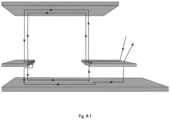
- the principle of operation of the holder according to the invention is based on the studied sample placed between the top plate and the bottom plate, inside the central opening in the middle plate, and then the bottom plate, the top plate and the middle plate are connected using the detachable connection.
- Such a connection of holder elements results in the sample being surrounded in the plane orthogonal to its top surface by a loop formed as a result of electrical contact between at least one bottom, conductive non-magnetic strip, at least one central, surrounding, conductive non-magnetic strip, at least one top, conductive non-magnetic strip and at least one central, surface, conductive non-magnetic strip.
- the free end of at least one bottom, conductive non-magnetic strip and the free end of at least one central, surface, conductive non-magnetic strip are connected, respectively, with poles of the microwave signal carrier connected to a microwave generator.
- the microwave source When the microwave source is turned on, coupling of the studied sample with microwave radiation may be achieved, wherein at least one top opening in the top plate ensures continuous optical access to the studied sample during the measurement, making studies using the ODMR method possible.
- the holder according to the invention does not require additional technological operations to be performed on the sample, such as metal sputtering or application of electrical contacts onto the sample.
- the design of the holder according to the invention ensures compatibility with the already existing systems and devices used in optical magnetospectroscopy.
- the described solution is characterised by its compact size and enables its use with a wide range of frequencies, as well as enables measurements in cryogenic temperatures.
- An additional advantage of the holder according to the invention lies in the fact that it enables the studied samples to be replaced repeatedly without a negative impact on functional parameters of the measurement system.
- the described holder additionally ensures advantageous direction of the magnetic component of microwave radiation towards the direction of the sampling light and towards the external magnetic field.
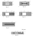
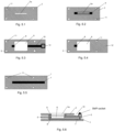
- a sample holder for measurements of optically detected magnetic resonance, which includes the bottom plate 1, the top plate 2 and the middle plate 5, wherein the bottom plate 1 has dimensions 25 mm x 60 mm x 1 mm, the top plate 2 has dimensions 25 mm x 45 mm x 1 mm, while the middle plate has dimensions 25 mm x 55 mm x 0.5 mm.
- the middle plate 5 is provided with a rectangular, central opening 6, which has dimensions 16 mm x 20 mm x 0.5 mm.
- the top opening is formed by two rectangular, top openings 3a and 3b, divided symmetrically along the longer side of the top plate 2 by a bridge 4, also made of FR-4, with a width of 1 mm.
- Connecting openings 11 with a 1.5 mm diameter are provided coaxially in all three plates, wherein brass screws with nuts made of the same material pass through said openings.
- the bottom, conductive non-magnetic strip 7 is provided, with a width of 1 mm, length of 46 mm and thickness of 35 ⁇ m, made of gold-plated copper.
- the bottom, conductive non-magnetic strip 7 is connected at its first end, via the SMP microwave socket, and through the socket opening 12, with the first pole of the microwave signal carrier, in the form of a microwave cable, while at its second end it forms an electrical connection with the first end of the central, surrounding, conductive non-magnetic strip 8, the width of which is equal to the width of the bottom, conductive non-magnetic strip 7 and is equal 1 mm, while its thickness is 100 ⁇ m.
- the central, surrounding, conductive non-magnetic strip 8 is placed on the middle plate 5 from the side of the central opening 6, transversely to the side of the middle plate 5, and its ends overlap both surfaces of the middle plate 5 by 2 mm each.
- the second end of the surrounding, conductive non-magnetic strip 8 forms an electrical connection with the first end of the top, conductive non-magnetic strip 9, the width of which is also 1 mm and which is placed on the surface of the top plate 2 oriented towards the bottom plate 1.
- the top, conductive non-magnetic strip 9 passes across the bridge 4.
- the second end of the top, conductive non-magnetic strip 9 forms an electrical connection with the first end of the central, surface, conductive non-magnetic strip 10 provided on the side of the middle plate 5 opposite to the central, surrounding, conductive non-magnetic strip 8 on the side of the middle plate 5, on the surface oriented towards the top plate 2.
- the width of the central, surface, conductive non-magnetic strip 10 is 1 mm.
- the second end of the central, surface, conductive non-magnetic strip 10 is connected with the second pole of the microwave signal carrier via the aforementioned, SMP microwave socket.
- the well was made using epitaxy, with molecular bundles, on a 350 micrometre thick substrate made of gallium arsenide, covered with a buffer layer of cadmium telluride, 5 micrometre thick.
- the sample dimensions were 5 mm x 5 mm x 0.35 mm.
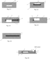
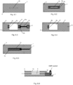
- the sample holder for measurements of optically detected magnetic resonance was prepared similarly to the first embodiment, with the difference that one rectangular top opening 3a with dimensions 8 mm x 20 mm x 0.5 mm is made in the top plate 2.
- the top opening 3a is placed asymmetrically in relation to the width of the plate, namely, is located closer to one of the longer sides of the top plate 2.
- the middle plate 5 is provided with a rectangular, central opening 6, which is locate asymmetrically, similar to opening 3a.
- the central opening 6 has dimensions of 16 mm x 20 mm x 0.5 mm and is located closer to one of the longer sides of the top plate 2, similar to the top opening 3a.
- the top, conductive non-magnetic strip 9, provided on the top plate 2 on the side of the bottom plate 1, is placed in parallel and at the same distance to the two longer sides of the top plate 2.
- the asymmetrical position of the central opening 6 implies that the surrounding, conductive non-magnetic strip 8 and the central, surface, conductive non-magnetic strip 10 are located closer to one of the two longer sides of the central opening 6.
- Bridge 4 is absent in this embodiment, wherein the other technical characteristics are analogous to the first embodiment of the invention.
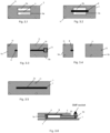
- a sample holder for measurements of optically detected magnetic resonance was prepared in the third embodiment of the invention, similarly to the first embodiment of the invention, with the difference that the central plate 5 comprises of two separated plates 5a and 5b, made of a dielectric material. Plates 5a and 5b are provided with connecting openings 11.
- a sample holder for measurements of optically detected magnetic resonance was prepared similarly to the first embodiment, with the difference that the top opening includes eight top openings 3a, 3b, 3c, 3d, 3e, 3f, 3g, 3h with a diameter of 1 mm in a series, wherein the top, conductive non-magnetic strip 9, provided on the top plate 2 on the side of the bottom plate 1, is placed in parallel and along the eight top openings 3a, 3b, 3c, 3d, 3e, 3f, 3g, 3h, comprising the top opening.
- Bridge 4 is absent in this sample holder according to the invention in this embodiment, wherein the other technical characteristics are analogous to the first embodiment of the invention.
- a sample holder for measurements of optically detected magnetic resonance was prepared similarly to the first embodiment, with the difference that only one, parallel and located at the same distance to the two longer sides of the top plate 2, rectangular top opening 3a with dimensions 0.5 mm x 16 mm x 0.5 mm is made in the top plate 2.
- bridge 4 is absent in the sample holder according to this embodiment, wherein the other technical characteristics are analogous to the first embodiment of the invention.
- a sample holder for measurements of optically detected magnetic resonance was prepared, which enables two parallel loops of the electrical circuits to be formed thanks to its design, thus additionally increasing the value of the magnetic component of the microwave on the sample surface.
- the holder according to this embodiment is similar to the holder according to the fifth embodiment of the invention, with the difference that the bottom, conductive non-magnetic strip 7 is separated into two parallel strip in the area of the central opening 6, i.e. into the bottom, conductive non-magnetic strip 7a and the bottom, conductive non-magnetic strip 7b.
- the bottom, conductive non-magnetic strip 7 is connected, via the SMP microwave socket, through the socket opening (12), with the first pole of the microwave signal carrier, provided in the form of a microwave cable.
- the central, surrounding, conductive non-magnetic strip 8, provided on the middle plate 5 on the side of the central opening 6, transversely to the side of the middle plate 6, is separated in this embodiment into two parallel strips, i.e. into the central, surrounding, conductive non-magnetic strip 8a and the central, surrounding, conductive non-magnetic strip 8b.
- the middle plate 5 has dimensions of 25 mm x 55 mm x 0.5 mm and is made of FR-4, wherein the central opening 6 has rectangular shape, with dimensions of 16 mm x 20 x 0.5 mm.
- the bottom, conductive non-magnetic strip 7a forms electrical connection with the first end of the central, surrounding, conductive non-magnetic strip 8a
- the bottom, conductive non-magnetic strip 7b forms electrical connection with the first end of the central, surrounding, conductive non-magnetic strip 8b.
- the top, conductive non-magnetic strip 9 is separated into two parallel strips, i.e. the top, conductive non-magnetic strip 9a and the top, conductive non-magnetic strip 9b.
- the dimensions of the top, conductive non-magnetic strip 9a are 1 mm x 25 mm, while the dimensions of the top, conductive non-magnetic strip 9b are 1 mm x 25 mm.
- the top opening 3 with dimensions of 1 mm x 25 mm x 0.5 mm is provided between the top, non-magnetic trip 9a and the top, conductive non-magnetic strip 9b.
- the second end of the central, surrounding, conductive non-magnetic strip 8a forms electrical connection with the first end of the top, conductive non-magnetic strip 9a
- the second end of the central, surrounding, conductive non-magnetic strip 8b forms electrical connection with the first end of the top, conductive non-magnetic strip 9b.
- the central, surface, conductive non-magnetic strip 10 is separated at its first end located at the central opening 6 into two parallel strips, i.e. the central, surface, conductive non-magnetic strip 10a and the central, surface, conductive non-magnetic strip 10b.
- the second end of the top, conductive non-magnetic strip 9a is connected with the first end of the central, surface, conductive non-magnetic strip 10a, while the second end of the first, conductive non-magnetic strip 9b is connected with the first end of the central, surface, conductive non-magnetic strip 10b.
- the second end of the central, surface, conductive non-magnetic strip 10a and the second end of the central, surface, conductive non-magnetic strip 10a connect and form the second end of the central, surface, conductive non-magnetic strip 10, which is connected with the second pole of the microwave signal carrier via the SMP microwave socket.
- This solution ensures increased homogeneity of the magnetic component of the microwave, as well as zero gradient of magnetic field along the axis between the conductive, conductive non-magnetic strips.
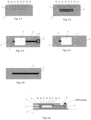
- a sample holder for measurements of optically detected magnetic resonance the design of which ensures formation of two spatially parallel loops of the electrical circuit, connected electrically in series.
- the holder includes the bottom plate 1, the top plate 2 and the middle plate 5, wherein the bottom plate 1 has dimensions 25 mm x 60 mm x 1 mm, the top plate 2 has dimensions 25 mm x 45 mm x 1 mm, while the middle plate has dimensions 25 mm x 55 mm x 0.5 mm.
- the middle plate 5 is provided with a rectangular, central opening 6, with dimensions of 16 mm x 20 mm x 0.5 mm, while the top plate 2 is provided with the top opening 3a with dimensions of 2 mm x 16 mm x 0.5 mm.
- the bottom plate 1, the top plate 2 and the middle plate 5 are made of FR-4.
- the central, surface, conductive non-magnetic strip 10 with 1 mm width, 20 mm length and 35 ⁇ m thickness is provided on the surface of the middle plate 5 oriented towards the top plate 2.
- the central, surface, conductive non-magnetic strip 10 is provided asymmetrically in relation to the width of the middle plate 5 and is located 8 mm away from one of the two longer edges of the middle plate 5 and 16 mm away from the other of the two longer edges of the middle plate 5.
- Two parallel strips, i.e. the top, conductive non-magnetic strip 9a and the top, conductive non-magnetic strip 9b, between which the top opening 3a is provided, are provided on the surface of the top plate 2 oriented towards the bottom plate 1.
- the central, surrounding, conductive non-magnetic strip 8, provided on the middle plate 5 on the side of the central opening 6, transversely to the side of the middle plate 6, is separated in this embodiment into two parallel strips, i.e. into the central, surrounding, conductive non-magnetic strip 8a and the central, surrounding, conductive non-magnetic strip 8b.
- a central, surrounding, conductive non-magnetic strip 8c is provided on the side of the central opening 6 opposite to the central, surrounding, conductive non-magnetic strip 8b, which is C-shaped and turned towards the central opening 6 on the surface of the middle plate 5 oriented towards the top plate 2.
- the bottom, conductive non-magnetic strip 7 is separated into two parallel strips, i.e. the bottom, conductive non-magnetic strip 7a and the bottom, conductive non-magnetic strip 7b.
- the bottom, conductive non-magnetic strip 7a is bent at a 90° angle towards the bottom, conductive non-magnetic strip 7b on the side of the SMP connector.
- the middle, surface, conductive non-magnetic strip 10 is connected at its first end with the first pole of the microwave signal carrier, provided as a microwave cable, using the SMP microwave socket.
- the second end of the central, surface, conductive non-magnetic strip 10 provided at the edge of the central opening 6 is connected with the first end of the top, conductive non-magnetic strip 9a.
- the second end of the top, conductive non-magnetic strip 9a is connected with the first end of the central, surrounding, conductive non-magnetic strip 8a, while the second end of the central, surrounding, conductive non-magnetic strip 8a is connected with the first end of the bottom, conductive non-magnetic strip 7a.
- the second end of the bottom, conductive non-magnetic strip 7a is connected with the first end of the central, surrounding, conductive non-magnetic strip 8c.
- the second end of the central, surrounding, conductive non-magnetic strip 7c is connected with the first end of the top, conductive non-magnetic strip 9b, while the second end of the top, conductive non-magnetic strip 9b is connected with the first end of the central, surrounding, conductive non-magnetic strip 8b, and the second end of the central, surrounding, conductive non-magnetic strip 8b is connected with the first end of the bottom, conductive non-magnetic strip 7b.
- the second end of the bottom, conductive non-magnetic strip 7 is connected, via the SMP microwave socket, through the socket opening (12), with the second pole of the microwave signal carrier, provided in the form of a microwave cable.
- a sample holder for measurements of optically detected magnetic resonance was prepared, similarly to the first embodiment, with the difference that the SMP microwave socket was rotated at an angle of 90° towards its initial orientation in the first embodiment of the invention.
- the SMP socket is connected, using a solder, at one of its poles with the conductive non-magnetic strip 10 of the middle plate 5, while at the other end is connected with the conductive non-magnetic strip 7 provided on the bottom plate 1.
- Such a modification of the SMP socket facilitates connection of a microwave cable, as well as placement of the handle according to the invention inside the laser beam.
Landscapes
- Physics & Mathematics (AREA)
- Condensed Matter Physics & Semiconductors (AREA)
- General Physics & Mathematics (AREA)
- Control Of Motors That Do Not Use Commutators (AREA)
- Investigating Or Analysing Materials By Optical Means (AREA)
- Magnetic Resonance Imaging Apparatus (AREA)
Applications Claiming Priority (2)
| Application Number | Priority Date | Filing Date | Title |
|---|---|---|---|
| PL431387A PL239882B1 (pl) | 2019-10-04 | 2019-10-04 | Uchwyt na próbkę do pomiarów optycznie wykrywanego rezonansu magnetycznego |
| PCT/IB2020/059288 WO2021064687A1 (en) | 2019-10-04 | 2020-10-02 | Sample holder for measurements of optically detected magnetic resonance |
Publications (2)
| Publication Number | Publication Date |
|---|---|
| EP4038403A1 EP4038403A1 (en) | 2022-08-10 |
| EP4038403B1 true EP4038403B1 (en) | 2024-09-18 |
Family
ID=73172762
Family Applications (1)
| Application Number | Title | Priority Date | Filing Date |
|---|---|---|---|
| EP20803642.6A Active EP4038403B1 (en) | 2019-10-04 | 2020-10-02 | Sample holder for measurements of optically detected magnetic resonance |
Country Status (4)
| Country | Link |
|---|---|
| US (1) | US12044758B2 (pl) |
| EP (1) | EP4038403B1 (pl) |
| PL (1) | PL239882B1 (pl) |
| WO (1) | WO2021064687A1 (pl) |
Families Citing this family (1)
| Publication number | Priority date | Publication date | Assignee | Title |
|---|---|---|---|---|
| DE102021120972A1 (de) * | 2021-08-11 | 2023-02-16 | Analytik Jena Gmbh | Vorrichtung für die Analyse einer als Tropfen bereitgestellten flüssigen oder pastösen Probe anhand von Kernspinresonanzen der Probe |
Family Cites Families (5)
| Publication number | Priority date | Publication date | Assignee | Title |
|---|---|---|---|---|
| JPS62132159A (ja) * | 1985-12-04 | 1987-06-15 | Nec Corp | トリプレ−ト型共振器 |
| JP4593255B2 (ja) * | 2004-12-08 | 2010-12-08 | 株式会社日立製作所 | Nmr装置およびnmr計測用プローブ |
| JP5973397B2 (ja) * | 2013-08-30 | 2016-08-23 | 日本電信電話株式会社 | 電子スピン共鳴装置 |
| US10585154B1 (en) * | 2018-01-29 | 2020-03-10 | Quantum Valley Investment Fund LP | Nuclear magnetic resonance diffraction |
| US11500186B2 (en) * | 2018-12-20 | 2022-11-15 | Massachusetts Institute Of Technology | Combined microscope objective and microwave wire for optically detected magnetic resonance imaging |
-
2019
- 2019-10-04 PL PL431387A patent/PL239882B1/pl unknown
-
2020
- 2020-10-02 EP EP20803642.6A patent/EP4038403B1/en active Active
- 2020-10-02 US US17/765,565 patent/US12044758B2/en active Active
- 2020-10-02 WO PCT/IB2020/059288 patent/WO2021064687A1/en not_active Ceased
Also Published As
| Publication number | Publication date |
|---|---|
| PL239882B1 (pl) | 2022-01-24 |
| WO2021064687A1 (en) | 2021-04-08 |
| PL431387A1 (pl) | 2021-04-06 |
| US20220404444A1 (en) | 2022-12-22 |
| EP4038403A1 (en) | 2022-08-10 |
| US12044758B2 (en) | 2024-07-23 |
Similar Documents
| Publication | Publication Date | Title |
|---|---|---|
| JP3834758B2 (ja) | 核磁気共鳴プローブ用コイル | |
| US5594342A (en) | Nuclear magnetic resonance probe coil with enhanced current-carrying capability | |
| US9507004B2 (en) | Electron spin resonance spectrometer and method for using same | |
| Gao et al. | Quantitative microwave near-field microscopy of dielectric properties | |
| JP4303286B2 (ja) | 超電導量子アンテナ | |
| EP1361452A2 (en) | Probe for NMR apparatus using magnesium diboride | |
| JPH11133127A (ja) | Nmr信号受信用超伝導ハイブリッド共鳴器 | |
| CN105158561A (zh) | 基于无氧铜矩形谐振腔的可调传输子量子比特系统 | |
| EP4038403B1 (en) | Sample holder for measurements of optically detected magnetic resonance | |
| Sauzade et al. | High resolution nuclear magnetic resonance spectroscopy in high magnetic fields | |
| Rinard et al. | Loop-gap resonators | |
| US11119165B2 (en) | Photonic band-gap resonator for magnetic resonance applications | |
| US8823373B2 (en) | Dual-resonance structure and method for examining samples using a plurality of conductive strips | |
| Sakai et al. | Electron paramagnetic resonance at high pressure using a diamond anvil cell | |
| Annino et al. | Dielectric resonators in ESR: overview, comments and perspectives | |
| Stenzel | High-frequency noise on antennas in plasmas | |
| Mamin et al. | Superconducting microwave resonator for millikelvin magnetic resonance force microscopy | |
| Klein | Basic concepts I | |
| Slade et al. | An esr spectrometer operating at 4 mm wavelength for the investigation of large zero field splittings | |
| US10571533B2 (en) | Method for manufacturing detection coil for magnetic resonance measurement | |
| Tkach et al. | W-band Fabry–Pérot microwave reasonators for optical detected electron paramagnetic resonance and electron nuclear double resonance of paramagnetic defects in solids | |
| Spaeth et al. | High‐field optically detected EPR and ENDOR of semiconductor defects using W‐band microwave Fabry–Pérot resonators | |
| Grzybowski et al. | Magnetic field probe for measuring surface current distributions on millimetre wave microstrip antennas | |
| Bai et al. | Spintronic terahertz emitter integrated multiple metasurface pattern for terahertz polarization modulation | |
| Peric et al. | Simple RF matching for NMR coils in ENDOR spectrometers |
Legal Events
| Date | Code | Title | Description |
|---|---|---|---|
| STAA | Information on the status of an ep patent application or granted ep patent |
Free format text: STATUS: UNKNOWN |
|
| STAA | Information on the status of an ep patent application or granted ep patent |
Free format text: STATUS: THE INTERNATIONAL PUBLICATION HAS BEEN MADE |
|
| PUAI | Public reference made under article 153(3) epc to a published international application that has entered the european phase |
Free format text: ORIGINAL CODE: 0009012 |
|
| STAA | Information on the status of an ep patent application or granted ep patent |
Free format text: STATUS: REQUEST FOR EXAMINATION WAS MADE |
|
| 17P | Request for examination filed |
Effective date: 20220325 |
|
| AK | Designated contracting states |
Kind code of ref document: A1 Designated state(s): AL AT BE BG CH CY CZ DE DK EE ES FI FR GB GR HR HU IE IS IT LI LT LU LV MC MK MT NL NO PL PT RO RS SE SI SK SM TR |
|
| DAV | Request for validation of the european patent (deleted) | ||
| DAX | Request for extension of the european patent (deleted) | ||
| STAA | Information on the status of an ep patent application or granted ep patent |
Free format text: STATUS: EXAMINATION IS IN PROGRESS |
|
| 17Q | First examination report despatched |
Effective date: 20230510 |
|
| GRAP | Despatch of communication of intention to grant a patent |
Free format text: ORIGINAL CODE: EPIDOSNIGR1 |
|
| STAA | Information on the status of an ep patent application or granted ep patent |
Free format text: STATUS: GRANT OF PATENT IS INTENDED |
|
| INTG | Intention to grant announced |
Effective date: 20240409 |
|
| GRAS | Grant fee paid |
Free format text: ORIGINAL CODE: EPIDOSNIGR3 |
|
| GRAA | (expected) grant |
Free format text: ORIGINAL CODE: 0009210 |
|
| STAA | Information on the status of an ep patent application or granted ep patent |
Free format text: STATUS: THE PATENT HAS BEEN GRANTED |
|
| AK | Designated contracting states |
Kind code of ref document: B1 Designated state(s): AL AT BE BG CH CY CZ DE DK EE ES FI FR GB GR HR HU IE IS IT LI LT LU LV MC MK MT NL NO PL PT RO RS SE SI SK SM TR |
|
| REG | Reference to a national code |
Ref country code: GB Ref legal event code: FG4D |
|
| REG | Reference to a national code |
Ref country code: CH Ref legal event code: EP |
|
| REG | Reference to a national code |
Ref country code: IE Ref legal event code: FG4D |
|
| REG | Reference to a national code |
Ref country code: DE Ref legal event code: R096 Ref document number: 602020038027 Country of ref document: DE |
|
| PGFP | Annual fee paid to national office [announced via postgrant information from national office to epo] |
Ref country code: DE Payment date: 20241217 Year of fee payment: 5 |
|
| REG | Reference to a national code |
Ref country code: LT Ref legal event code: MG9D |
|
| PG25 | Lapsed in a contracting state [announced via postgrant information from national office to epo] |
Ref country code: NO Free format text: LAPSE BECAUSE OF FAILURE TO SUBMIT A TRANSLATION OF THE DESCRIPTION OR TO PAY THE FEE WITHIN THE PRESCRIBED TIME-LIMIT Effective date: 20241218 |
|
| PG25 | Lapsed in a contracting state [announced via postgrant information from national office to epo] |
Ref country code: GR Free format text: LAPSE BECAUSE OF FAILURE TO SUBMIT A TRANSLATION OF THE DESCRIPTION OR TO PAY THE FEE WITHIN THE PRESCRIBED TIME-LIMIT Effective date: 20241219 Ref country code: FI Free format text: LAPSE BECAUSE OF FAILURE TO SUBMIT A TRANSLATION OF THE DESCRIPTION OR TO PAY THE FEE WITHIN THE PRESCRIBED TIME-LIMIT Effective date: 20240918 |
|
| PGFP | Annual fee paid to national office [announced via postgrant information from national office to epo] |
Ref country code: GB Payment date: 20241219 Year of fee payment: 5 |
|
| PG25 | Lapsed in a contracting state [announced via postgrant information from national office to epo] |
Ref country code: BG Free format text: LAPSE BECAUSE OF FAILURE TO SUBMIT A TRANSLATION OF THE DESCRIPTION OR TO PAY THE FEE WITHIN THE PRESCRIBED TIME-LIMIT Effective date: 20240918 |
|
| PG25 | Lapsed in a contracting state [announced via postgrant information from national office to epo] |
Ref country code: LV Free format text: LAPSE BECAUSE OF FAILURE TO SUBMIT A TRANSLATION OF THE DESCRIPTION OR TO PAY THE FEE WITHIN THE PRESCRIBED TIME-LIMIT Effective date: 20240918 |
|
| PG25 | Lapsed in a contracting state [announced via postgrant information from national office to epo] |
Ref country code: HR Free format text: LAPSE BECAUSE OF FAILURE TO SUBMIT A TRANSLATION OF THE DESCRIPTION OR TO PAY THE FEE WITHIN THE PRESCRIBED TIME-LIMIT Effective date: 20240918 |
|
| REG | Reference to a national code |
Ref country code: NL Ref legal event code: MP Effective date: 20240918 |
|
| PG25 | Lapsed in a contracting state [announced via postgrant information from national office to epo] |
Ref country code: RS Free format text: LAPSE BECAUSE OF FAILURE TO SUBMIT A TRANSLATION OF THE DESCRIPTION OR TO PAY THE FEE WITHIN THE PRESCRIBED TIME-LIMIT Effective date: 20241218 |
|
| PG25 | Lapsed in a contracting state [announced via postgrant information from national office to epo] |
Ref country code: RS Free format text: LAPSE BECAUSE OF FAILURE TO SUBMIT A TRANSLATION OF THE DESCRIPTION OR TO PAY THE FEE WITHIN THE PRESCRIBED TIME-LIMIT Effective date: 20241218 Ref country code: NO Free format text: LAPSE BECAUSE OF FAILURE TO SUBMIT A TRANSLATION OF THE DESCRIPTION OR TO PAY THE FEE WITHIN THE PRESCRIBED TIME-LIMIT Effective date: 20241218 Ref country code: LV Free format text: LAPSE BECAUSE OF FAILURE TO SUBMIT A TRANSLATION OF THE DESCRIPTION OR TO PAY THE FEE WITHIN THE PRESCRIBED TIME-LIMIT Effective date: 20240918 Ref country code: HR Free format text: LAPSE BECAUSE OF FAILURE TO SUBMIT A TRANSLATION OF THE DESCRIPTION OR TO PAY THE FEE WITHIN THE PRESCRIBED TIME-LIMIT Effective date: 20240918 Ref country code: GR Free format text: LAPSE BECAUSE OF FAILURE TO SUBMIT A TRANSLATION OF THE DESCRIPTION OR TO PAY THE FEE WITHIN THE PRESCRIBED TIME-LIMIT Effective date: 20241219 Ref country code: FI Free format text: LAPSE BECAUSE OF FAILURE TO SUBMIT A TRANSLATION OF THE DESCRIPTION OR TO PAY THE FEE WITHIN THE PRESCRIBED TIME-LIMIT Effective date: 20240918 Ref country code: BG Free format text: LAPSE BECAUSE OF FAILURE TO SUBMIT A TRANSLATION OF THE DESCRIPTION OR TO PAY THE FEE WITHIN THE PRESCRIBED TIME-LIMIT Effective date: 20240918 |
|
| REG | Reference to a national code |
Ref country code: AT Ref legal event code: MK05 Ref document number: 1725149 Country of ref document: AT Kind code of ref document: T Effective date: 20240918 |
|
| PG25 | Lapsed in a contracting state [announced via postgrant information from national office to epo] |
Ref country code: NL Free format text: LAPSE BECAUSE OF FAILURE TO SUBMIT A TRANSLATION OF THE DESCRIPTION OR TO PAY THE FEE WITHIN THE PRESCRIBED TIME-LIMIT Effective date: 20240918 |
|
| PG25 | Lapsed in a contracting state [announced via postgrant information from national office to epo] |
Ref country code: PT Free format text: LAPSE BECAUSE OF FAILURE TO SUBMIT A TRANSLATION OF THE DESCRIPTION OR TO PAY THE FEE WITHIN THE PRESCRIBED TIME-LIMIT Effective date: 20250120 Ref country code: IS Free format text: LAPSE BECAUSE OF FAILURE TO SUBMIT A TRANSLATION OF THE DESCRIPTION OR TO PAY THE FEE WITHIN THE PRESCRIBED TIME-LIMIT Effective date: 20250118 |
|
| PG25 | Lapsed in a contracting state [announced via postgrant information from national office to epo] |
Ref country code: SM Free format text: LAPSE BECAUSE OF FAILURE TO SUBMIT A TRANSLATION OF THE DESCRIPTION OR TO PAY THE FEE WITHIN THE PRESCRIBED TIME-LIMIT Effective date: 20240918 Ref country code: RO Free format text: LAPSE BECAUSE OF FAILURE TO SUBMIT A TRANSLATION OF THE DESCRIPTION OR TO PAY THE FEE WITHIN THE PRESCRIBED TIME-LIMIT Effective date: 20240918 |
|
| PG25 | Lapsed in a contracting state [announced via postgrant information from national office to epo] |
Ref country code: ES Free format text: LAPSE BECAUSE OF FAILURE TO SUBMIT A TRANSLATION OF THE DESCRIPTION OR TO PAY THE FEE WITHIN THE PRESCRIBED TIME-LIMIT Effective date: 20240918 |
|
| PG25 | Lapsed in a contracting state [announced via postgrant information from national office to epo] |
Ref country code: AT Free format text: LAPSE BECAUSE OF FAILURE TO SUBMIT A TRANSLATION OF THE DESCRIPTION OR TO PAY THE FEE WITHIN THE PRESCRIBED TIME-LIMIT Effective date: 20240918 Ref country code: EE Free format text: LAPSE BECAUSE OF FAILURE TO SUBMIT A TRANSLATION OF THE DESCRIPTION OR TO PAY THE FEE WITHIN THE PRESCRIBED TIME-LIMIT Effective date: 20240918 |
|
| PG25 | Lapsed in a contracting state [announced via postgrant information from national office to epo] |
Ref country code: PL Free format text: LAPSE BECAUSE OF FAILURE TO SUBMIT A TRANSLATION OF THE DESCRIPTION OR TO PAY THE FEE WITHIN THE PRESCRIBED TIME-LIMIT Effective date: 20240918 Ref country code: CZ Free format text: LAPSE BECAUSE OF FAILURE TO SUBMIT A TRANSLATION OF THE DESCRIPTION OR TO PAY THE FEE WITHIN THE PRESCRIBED TIME-LIMIT Effective date: 20240918 |
|
| PG25 | Lapsed in a contracting state [announced via postgrant information from national office to epo] |
Ref country code: SK Free format text: LAPSE BECAUSE OF FAILURE TO SUBMIT A TRANSLATION OF THE DESCRIPTION OR TO PAY THE FEE WITHIN THE PRESCRIBED TIME-LIMIT Effective date: 20240918 Ref country code: IT Free format text: LAPSE BECAUSE OF FAILURE TO SUBMIT A TRANSLATION OF THE DESCRIPTION OR TO PAY THE FEE WITHIN THE PRESCRIBED TIME-LIMIT Effective date: 20240918 |
|
| REG | Reference to a national code |
Ref country code: CH Ref legal event code: PL |
|
| REG | Reference to a national code |
Ref country code: DE Ref legal event code: R097 Ref document number: 602020038027 Country of ref document: DE |
|
| PG25 | Lapsed in a contracting state [announced via postgrant information from national office to epo] |
Ref country code: MC Free format text: LAPSE BECAUSE OF FAILURE TO SUBMIT A TRANSLATION OF THE DESCRIPTION OR TO PAY THE FEE WITHIN THE PRESCRIBED TIME-LIMIT Effective date: 20240918 |
|
| PG25 | Lapsed in a contracting state [announced via postgrant information from national office to epo] |
Ref country code: DK Free format text: LAPSE BECAUSE OF FAILURE TO SUBMIT A TRANSLATION OF THE DESCRIPTION OR TO PAY THE FEE WITHIN THE PRESCRIBED TIME-LIMIT Effective date: 20240918 |
|
| PG25 | Lapsed in a contracting state [announced via postgrant information from national office to epo] |
Ref country code: BE Free format text: LAPSE BECAUSE OF NON-PAYMENT OF DUE FEES Effective date: 20241031 Ref country code: LU Free format text: LAPSE BECAUSE OF NON-PAYMENT OF DUE FEES Effective date: 20241002 |
|
| PG25 | Lapsed in a contracting state [announced via postgrant information from national office to epo] |
Ref country code: CH Free format text: LAPSE BECAUSE OF NON-PAYMENT OF DUE FEES Effective date: 20241031 |
|
| PLBE | No opposition filed within time limit |
Free format text: ORIGINAL CODE: 0009261 |
|
| STAA | Information on the status of an ep patent application or granted ep patent |
Free format text: STATUS: NO OPPOSITION FILED WITHIN TIME LIMIT |
|
| REG | Reference to a national code |
Ref country code: BE Ref legal event code: MM Effective date: 20241031 |
|
| 26N | No opposition filed |
Effective date: 20250619 |
|
| PG25 | Lapsed in a contracting state [announced via postgrant information from national office to epo] |
Ref country code: SE Free format text: LAPSE BECAUSE OF FAILURE TO SUBMIT A TRANSLATION OF THE DESCRIPTION OR TO PAY THE FEE WITHIN THE PRESCRIBED TIME-LIMIT Effective date: 20240918 |
|
| PG25 | Lapsed in a contracting state [announced via postgrant information from national office to epo] |
Ref country code: FR Free format text: LAPSE BECAUSE OF NON-PAYMENT OF DUE FEES Effective date: 20241118 |
|
| PG25 | Lapsed in a contracting state [announced via postgrant information from national office to epo] |
Ref country code: IE Free format text: LAPSE BECAUSE OF NON-PAYMENT OF DUE FEES Effective date: 20241002 |
|
| PG25 | Lapsed in a contracting state [announced via postgrant information from national office to epo] |
Ref country code: CY Free format text: LAPSE BECAUSE OF FAILURE TO SUBMIT A TRANSLATION OF THE DESCRIPTION OR TO PAY THE FEE WITHIN THE PRESCRIBED TIME-LIMIT; INVALID AB INITIO Effective date: 20201002 |
|
| PG25 | Lapsed in a contracting state [announced via postgrant information from national office to epo] |
Ref country code: HU Free format text: LAPSE BECAUSE OF FAILURE TO SUBMIT A TRANSLATION OF THE DESCRIPTION OR TO PAY THE FEE WITHIN THE PRESCRIBED TIME-LIMIT; INVALID AB INITIO Effective date: 20201002 |