EP4037109B1 - Steckverbindersatz und kappe - Google Patents
Steckverbindersatz und kappe Download PDFInfo
- Publication number
- EP4037109B1 EP4037109B1 EP21217687.9A EP21217687A EP4037109B1 EP 4037109 B1 EP4037109 B1 EP 4037109B1 EP 21217687 A EP21217687 A EP 21217687A EP 4037109 B1 EP4037109 B1 EP 4037109B1
- Authority
- EP
- European Patent Office
- Prior art keywords
- connector
- thermal expansion
- expansion coefficient
- cap
- type connector
- Prior art date
- Legal status (The legal status is an assumption and is not a legal conclusion. Google has not performed a legal analysis and makes no representation as to the accuracy of the status listed.)
- Active
Links
Images


Classifications
-
- H—ELECTRICITY
- H01—ELECTRIC ELEMENTS
- H01R—ELECTRICALLY-CONDUCTIVE CONNECTIONS; STRUCTURAL ASSOCIATIONS OF A PLURALITY OF MUTUALLY-INSULATED ELECTRICAL CONNECTING ELEMENTS; COUPLING DEVICES; CURRENT COLLECTORS
- H01R24/00—Two-part coupling devices, or either of their cooperating parts, characterised by their overall structure
-
- H—ELECTRICITY
- H01—ELECTRIC ELEMENTS
- H01R—ELECTRICALLY-CONDUCTIVE CONNECTIONS; STRUCTURAL ASSOCIATIONS OF A PLURALITY OF MUTUALLY-INSULATED ELECTRICAL CONNECTING ELEMENTS; COUPLING DEVICES; CURRENT COLLECTORS
- H01R12/00—Structural associations of a plurality of mutually-insulated electrical connecting elements, specially adapted for printed circuits, e.g. printed circuit boards [PCB], flat or ribbon cables, or like generally planar structures, e.g. terminal strips, terminal blocks; Coupling devices specially adapted for printed circuits, flat or ribbon cables, or like generally planar structures; Terminals specially adapted for contact with, or insertion into, printed circuits, flat or ribbon cables, or like generally planar structures
- H01R12/70—Coupling devices
- H01R12/7005—Guiding, mounting, polarizing or locking means; Extractors
- H01R12/7011—Locking or fixing a connector to a PCB
- H01R12/707—Soldering or welding
-
- H—ELECTRICITY
- H01—ELECTRIC ELEMENTS
- H01R—ELECTRICALLY-CONDUCTIVE CONNECTIONS; STRUCTURAL ASSOCIATIONS OF A PLURALITY OF MUTUALLY-INSULATED ELECTRICAL CONNECTING ELEMENTS; COUPLING DEVICES; CURRENT COLLECTORS
- H01R12/00—Structural associations of a plurality of mutually-insulated electrical connecting elements, specially adapted for printed circuits, e.g. printed circuit boards [PCB], flat or ribbon cables, or like generally planar structures, e.g. terminal strips, terminal blocks; Coupling devices specially adapted for printed circuits, flat or ribbon cables, or like generally planar structures; Terminals specially adapted for contact with, or insertion into, printed circuits, flat or ribbon cables, or like generally planar structures
- H01R12/70—Coupling devices
- H01R12/71—Coupling devices for rigid printing circuits or like structures
- H01R12/712—Coupling devices for rigid printing circuits or like structures co-operating with the surface of the printed circuit or with a coupling device exclusively provided on the surface of the printed circuit
- H01R12/716—Coupling device provided on the PCB
-
- H—ELECTRICITY
- H01—ELECTRIC ELEMENTS
- H01R—ELECTRICALLY-CONDUCTIVE CONNECTIONS; STRUCTURAL ASSOCIATIONS OF A PLURALITY OF MUTUALLY-INSULATED ELECTRICAL CONNECTING ELEMENTS; COUPLING DEVICES; CURRENT COLLECTORS
- H01R12/00—Structural associations of a plurality of mutually-insulated electrical connecting elements, specially adapted for printed circuits, e.g. printed circuit boards [PCB], flat or ribbon cables, or like generally planar structures, e.g. terminal strips, terminal blocks; Coupling devices specially adapted for printed circuits, flat or ribbon cables, or like generally planar structures; Terminals specially adapted for contact with, or insertion into, printed circuits, flat or ribbon cables, or like generally planar structures
- H01R12/70—Coupling devices
- H01R12/71—Coupling devices for rigid printing circuits or like structures
- H01R12/72—Coupling devices for rigid printing circuits or like structures coupling with the edge of the rigid printed circuits or like structures
- H01R12/73—Coupling devices for rigid printing circuits or like structures coupling with the edge of the rigid printed circuits or like structures connecting to other rigid printed circuits or like structures
-
- H—ELECTRICITY
- H01—ELECTRIC ELEMENTS
- H01R—ELECTRICALLY-CONDUCTIVE CONNECTIONS; STRUCTURAL ASSOCIATIONS OF A PLURALITY OF MUTUALLY-INSULATED ELECTRICAL CONNECTING ELEMENTS; COUPLING DEVICES; CURRENT COLLECTORS
- H01R13/00—Details of coupling devices of the kinds covered by groups H01R12/70 or H01R24/00 - H01R33/00
- H01R13/46—Bases; Cases
- H01R13/502—Bases; Cases composed of different pieces
-
- H—ELECTRICITY
- H01—ELECTRIC ELEMENTS
- H01R—ELECTRICALLY-CONDUCTIVE CONNECTIONS; STRUCTURAL ASSOCIATIONS OF A PLURALITY OF MUTUALLY-INSULATED ELECTRICAL CONNECTING ELEMENTS; COUPLING DEVICES; CURRENT COLLECTORS
- H01R43/00—Apparatus or processes specially adapted for manufacturing, assembling, maintaining, or repairing of line connectors or current collectors or for joining electric conductors
- H01R43/02—Apparatus or processes specially adapted for manufacturing, assembling, maintaining, or repairing of line connectors or current collectors or for joining electric conductors for soldered or welded connections
- H01R43/0256—Apparatus or processes specially adapted for manufacturing, assembling, maintaining, or repairing of line connectors or current collectors or for joining electric conductors for soldered or welded connections for soldering or welding connectors to a printed circuit board
-
- H—ELECTRICITY
- H01—ELECTRIC ELEMENTS
- H01R—ELECTRICALLY-CONDUCTIVE CONNECTIONS; STRUCTURAL ASSOCIATIONS OF A PLURALITY OF MUTUALLY-INSULATED ELECTRICAL CONNECTING ELEMENTS; COUPLING DEVICES; CURRENT COLLECTORS
- H01R43/00—Apparatus or processes specially adapted for manufacturing, assembling, maintaining, or repairing of line connectors or current collectors or for joining electric conductors
- H01R43/02—Apparatus or processes specially adapted for manufacturing, assembling, maintaining, or repairing of line connectors or current collectors or for joining electric conductors for soldered or welded connections
- H01R43/0263—Apparatus or processes specially adapted for manufacturing, assembling, maintaining, or repairing of line connectors or current collectors or for joining electric conductors for soldered or welded connections for positioning or holding parts during soldering or welding process
-
- H—ELECTRICITY
- H05—ELECTRIC TECHNIQUES NOT OTHERWISE PROVIDED FOR
- H05K—PRINTED CIRCUITS; CASINGS OR CONSTRUCTIONAL DETAILS OF ELECTRIC APPARATUS; MANUFACTURE OF ASSEMBLAGES OF ELECTRICAL COMPONENTS
- H05K1/00—Printed circuits
- H05K1/02—Details
- H05K1/14—Structural association of two or more printed circuits
- H05K1/144—Stacked arrangements of planar printed circuit boards
-
- H—ELECTRICITY
- H05—ELECTRIC TECHNIQUES NOT OTHERWISE PROVIDED FOR
- H05K—PRINTED CIRCUITS; CASINGS OR CONSTRUCTIONAL DETAILS OF ELECTRIC APPARATUS; MANUFACTURE OF ASSEMBLAGES OF ELECTRICAL COMPONENTS
- H05K2201/00—Indexing scheme relating to printed circuits covered by H05K1/00
- H05K2201/10—Details of components or other objects attached to or integrated in a printed circuit board
- H05K2201/10007—Types of components
- H05K2201/10189—Non-printed connector
-
- H—ELECTRICITY
- H05—ELECTRIC TECHNIQUES NOT OTHERWISE PROVIDED FOR
- H05K—PRINTED CIRCUITS; CASINGS OR CONSTRUCTIONAL DETAILS OF ELECTRIC APPARATUS; MANUFACTURE OF ASSEMBLAGES OF ELECTRICAL COMPONENTS
- H05K3/00—Apparatus or processes for manufacturing printed circuits
- H05K3/30—Assembling printed circuits with electric components, e.g. with resistors
- H05K3/32—Assembling printed circuits with electric components, e.g. with resistors electrically connecting electric components or wires to printed circuits
- H05K3/34—Assembling printed circuits with electric components, e.g. with resistors electrically connecting electric components or wires to printed circuits by soldering
- H05K3/341—Surface mounted components
- H05K3/3431—Leadless components
- H05K3/3436—Leadless components having an array of bottom contacts, e.g. pad grid array or ball grid array components
Definitions
- the present disclosure relates to a high-speed transmission connector to be mounted on a circuit board, in particular, to a mezzanine connector that electrically connects different circuit boards.
- connectors for mediating high-speed transmission of signals between a circuit board and an expansion board there is a type of connector in which the connector mounted on the circuit board side is a socket type, the connector mounted on the expansion board side is a plug type, and the terminals of both connectors are electrically connected by fitting the plug type connector to the frontage of the socket type connector.
- this type of connector is called mezzanine connector.
- Patent Document 1 Japanese Patent Application Publication No. 2018-113146
- the connector described in this document has a box-shaped housing and contacts arranged side by side on its wall surface.
- the bottom surface of the housing of this connector is provided with a boss inserted into a positioning hole in a circuit board, and contacts are provided at the frontage on the side opposite to the side with the boss in the housing.
- the reflow mounting of this type of connector on a board is performed by placing the connector at a predetermined position on the board with the cap attached, raising the temperature from ordinary temperature to about 260 degrees to melt the solder, and returning it to ordinary temperature.
- Patent document US 2010/304584 discloses a connector set including at least one of a header and a socket and a jointer.
- the jointer extends in a direction and is configured to couple the header and the socket so as to be in parallel with each other.
- the jointer includes first jointer connecting portions provided at both end portions thereof and extending in a second direction perpendicular to the first direction, and which are configured to engage first connecting portions provided at both end portions of the header, and second jointer connecting portions provided at both end portions of the jointer body and extending in a third direction opposite to the second direction, and which are configured to engage the second connecting portions provided at both end portions of the socket.
- the invention corresponds to the connector set as disclosed in claim 1.
- a connector set including: a first connector; a first cap to be attached to the first connector when the first connector is reflow-mounted on a first external substrate; a second connector; and a second cap to be attached to the second connector when the second connector is reflow-mounted on a second external substrate formed of a material with a smaller thermal expansion coefficient than that of the first external substrate, wherein the second cap is formed of a material with a smaller thermal expansion coefficient than that of the first cap.
- the first connector includes a first housing with a slot and a plurality of contacts arranged in the slot
- the second connector includes a second housing with a header to be fitted in the slot.
- the first connector is arranged in a direction orthogonal to an extending direction of the slot and held by the first cap
- the second connector is arranged in a direction orthogonal to an extending direction of the header and held by the second cap.
- the relation of the ratio ⁇ 11/ ⁇ 10 of a thermal expansion coefficient ⁇ 11 to a thermal expansion coefficient ⁇ 10 and the ratio ⁇ 21/ ⁇ 20 of the thermal expansion coefficient ⁇ 21 to a thermal expansion coefficient ⁇ 20 may be ⁇ 11/ ⁇ 10 ⁇ ⁇ 21/ ⁇ 20, here the thermal expansion coefficient ⁇ 11 is the thermal expansion coefficient of the first cap in an arrangement direction of the first connector, the thermal expansion coefficient ⁇ 10 is the thermal expansion coefficient of the first external substrate, the thermal expansion coefficient ⁇ 21 is the thermal expansion coefficient of the second cap in an arrangement direction of the second connector, and the thermal expansion coefficient ⁇ 20 is the thermal expansion coefficient of the second external substrate.
- the number of the slots in one first connector may be two, and the number of the headers in one second connector may be two.
- the position of the contact on one side and the position of the contact on the other side may be shifted by 1/2 contact.
- first housing and the second housing may have a rotationally asymmetrical shape as viewed from the fitting direction.
- the first housing may include a bottom portion, first wall portions facing each other in a first direction orthogonal to the fitting direction, and second wall portions facing each other in a second direction orthogonal to the fitting direction and the first direction, so as to surround the slot.
- the slot may be separated into a plurality of slots by a partition wall extending along the first direction, one end portion of the partition wall may be connected to one first wall portion of the two first wall portions on both sides of the first direction, the other end portion of the partition wall may be not connected to the other first wall portion.
- a gap may be formed between the other end portion of the partition wall and the other first wall portion.
- the second housing may include a plurality of headers. The plurality of headers may extend in the first direction, and a fitting plate portion to be fitted in the gap may be provided between the adjacent one end portions of the plurality of headers in the first direction.
- a connector set including: a first connector; a first cap to be attached to the first connector when the first connector is reflow-mounted on a first external substrate; a second connector; and a second cap to be attached to the second connector when the second connector is reflow-mounted on a second external substrate formed of a material with a smaller thermal expansion coefficient than that of the first external substrate, the first cap and the second cap are formed of different materials in such a manner that a mounting position error is less than 0.15 mm when the first cap is reflow-mounted on the first external substrate and the second cap is reflow-mounted on the second external substrate.
- a cap including: a first cap to be attached to a first connector when the first connector is reflow-mounted on a first external substrate; a second connector; and a second cap to be attached to the second connector when the second connector is reflow-mounted on a second external substrate formed of a material with a smaller thermal expansion coefficient than that of the first external substrate, wherein the second cap is formed of a material with a smaller thermal expansion coefficient than that of the first cap.
- the relation of the ratio ⁇ 11/ ⁇ 10 of the thermal expansion coefficient ⁇ 11 to the thermal expansion coefficient ⁇ 10 and the ratio ⁇ 21/ ⁇ 20 of the thermal expansion coefficient ⁇ 21 to the thermal expansion coefficient ⁇ 20 may be ⁇ 11/ ⁇ 10 ⁇ ⁇ 21/ ⁇ 20, here the thermal expansion coefficient ⁇ 11 is the thermal expansion coefficient of the first cap in an arrangement direction of the first connector, the thermal expansion coefficient ⁇ 10 is the thermal expansion coefficient of the first external substrate, the thermal expansion coefficient ⁇ 21 is the thermal expansion coefficient of the second cap in an arrangement direction of the second connector, and the thermal expansion coefficient ⁇ 20 is the thermal expansion coefficient of the second external substrate.
- a socket type connector 1, a plug type connector 2, a first cap 100, and a second cap 200 that form a connector set according to one embodiment of the present disclosure will be explained with reference to drawings.
- a plurality of (four in the example of Fig. 1 ) socket type connectors 1 and plug type connectors 2 are arranged side by side, and are respectively mounted on a first substrate 51 and a second substrate 52.
- the second substrate 52 is formed of a material with a lower thermal expansion coefficient than that of the first substrate 51.
- the material of the first substrate 51 is FR4 (Flame Retardant Type 4), and the material of the second substrate 52 is ceramic.
- the first cap 100 is attached to the socket type connectors 1 when the socket type connectors 1 are reflow-mounted on the first substrate 51.
- the second cap 200 is attached to the plug type connectors 2 when the plug type connectors 2 are reflow-mounted on the second substrate 52.
- the fitting direction of the plug type connector 2 to the socket type connector 1 is appropriately referred to as the Z direction
- the direction orthogonal to the Z direction is appropriately referred to as the X direction
- the direction orthogonal to the Z direction and the X direction is appropriately referred to as the Y direction.
- the +Z side may be referred to as an upper side
- the -Z side may be referred to as a lower side
- the +X side may be referred to as a front side
- the -X side may be referred to as a rear side
- the +Y side may be referred to as a left side
- the -Y side may be referred to as a right side.
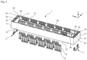
- the socket type connector 1 has a first housing 10, solder tab terminals 7 and contacts 8.
- the plug type connector 2 has a second housing 20, solder tab terminals 7 and contacts 8.
- the first housing 10 of the socket type connector 1 and the second housing 20 of the plug type connector 2 are formed by injecting resin in the X direction which is the longitudinal direction.
- the first housing 10 of the socket type connector 1 and the second housing 20 of the plug type connector 2 have a rotationally asymmetrical shape.
- the socket type connector 1 corresponds to, for example, the first connector defined in claims and the plug type connector 2 corresponds to, for example, the second connector defined in claims.
- the first housing 10 of the socket type connector 1 is provided with two slots 19.
- the two slots 19 extend in the X direction.
- the first housing 10 has a bottom portion 13 that becomes the bottom of the housing 10, wall portions 11 and wall portions 12 respectively facing each other in the X direction and the Y direction so as to surround the slots 19, and a partition wall 17 separating the two slots 19 in a frontage surrounded by the wall portions 11 and the wall portions 12.
- the wall portions 11 extend in the Y direction
- the wall portions 12 extend in the X direction.
- the wall portions 11 and the wall portions 12 correspond to, for example, the first wall portions and the second wall portions that are defined in claims, respectively.
- the end portion of the partition wall 17 on the -X side is connected to the wall portion 11 on the -X side.
- the end portion of the partition wall 17 on the +X side is not connected to the wall portion 11 on the +X side, and a gap 18 is formed between the end portion of the partition wall 17 on the +X side and the wall portion 11 on the +X side.
- a round hole 31 is provided in the middle of the wall portion 11 on the -X side in the Y direction.
- a long hole 33 is provided in the middle of the wall portion 11 on the +X side in the Y direction.
- the +X side of the long hole 33 is open.
- Rectangular grooves 35 are provided on the +Y side and the -Y side of the holes in the wall portion 11 on the -X side and the wall portion 11 on the +X side.
- the rectangular grooves 35 are recessed from the upper surfaces of the wall portions 11 toward the bottom portion 13. Holes are perforated at the bottoms of the rectangular grooves 35, and the solder tab terminals 7 are fitted and fixed in the holes. As shown in Fig.
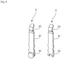
- the solder tab terminal 7 has an elongated substrate portion 71 and two projecting piece portions 72 rising from two end portions of one long side of the substrate portion 71.
- the two projecting piece portions 72 are fitted into the holes at the bottom of the rectangular groove 35 of the first housing 10.
- Grooves 36 are provided in the inner surfaces of the wall portions 12 and the side surfaces of the partition wall 17. Contacts 8 are accommodated in the grooves 36. As shown in Fig. 9 , the contact 8 has a linear portion 81 extending in one direction, a terminal portion 82 at one end of the linear portion 81, and a fork portion 83 at the other end of the linear portion 81. The terminal portion 82 is bent into a doglegged shape. The fork portion 83 is bifurcated. Solder 9 is caulked and fixed to the fork portion 83. The contact 8 is held in the grooves 36 of the wall portion 12 and the partition wall 17, and the fork portion 83 of the contact 8 and the solder 9 are exposed to the opposite side to the groove 36 side through the hole in the bottom portion 13.
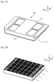
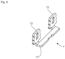
- the first cap 100 has a box shape with a width in the X direction and the Y direction slightly larger than that of four socket type connectors 1 arranged side by side.
- a first opening 130 for accommodating and holding the socket type connectors 1 is provided on the -Z side of the first cap 100.
- the first cap 100 has a top plate portion 113 that constitutes a ceiling of the first cap 100, wall portions 111 and wall portions 112 respectively facing each other in the X direction and the Y direction across the first opening 130.
- a hooking spring 135 and a spring accommodation portion 136 are provided at a position corresponding to each slot 19 of four first housings 10 inside the wall portion 112 on the -X side and the wall portion 112 on the +X side. As shown in Fig. 14 , the lower end portion 134 of the hooking spring 135 projects outward in a triangular shape.
- a positioning pin is provided at a position corresponding to the round hole 31 between the adjacent spring accommodation portions 136 inside the wall portion 112 on the -X side.
- the positioning pin has a shape to be put in the round hole 31.
- a positioning long pin is provided at a position corresponding to the long hole 33 between the adjacent spring accommodation portions 136 inside the wall portion 112 on the +X side. The positioning long pin has a shape to be put in the long hole 33.
- the attachment of the first cap 100 to the socket type connector 1 and the reflow mounting thereof are performed as follows. First, the four socket type connectors 1 are arranged so that the orientation of the gaps 18 of a part of the socket type connectors 1 and the orientation of the gaps 18 of the remaining socket type connectors 1 are reversed (for example, the gaps 18 of two socket type connectors 1 in the middle are on the -X side, and the gaps 18 of two socket type connectors 1 at both ends are on the +X side).
- the first cap 100 is attached to the four socket type connectors 1 so that the positioning pins are inserted into the round holes 31 on the -X side, the positioning long pins are inserted into the long holes 33 on the +X side, and the hooking springs 135 are fitted inside the wall portions 11 on the -X side and the +X side.
- the lower end portions 134 of the hooking springs 135 of the first cap 100 engage with the engaging pieces 34 of the connectors 1, and the socket type connectors 1 are supported from the inside in the X direction by the hooking springs 135 of the first cap 100.
- the four socket type connectors 1 gathered by the first cap 100 are placed on a predetermined position of the first substrate 51, and are put into a reflow device.
- the temperature in the device is changed from 20 °C to 260°C to 20°C.
- the solder 9 at the tip end portion of the contact 8 is melted, and when the temperature returns to ordinary temperature, the solder 9 solidifies.
- the contact 8 of the socket type connector 1 and the pad of the first substrate 51 are connected to each other by the solidification of the solder 9.
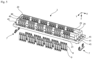
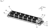
- the second housing 20 of the plug type connector 2 is provided with two headers 29.
- the two headers 29 extend in the X direction.
- the end portions on the -X side, +X side, -Y side, and +Y side of the bottom portion 23 that becomes the bottom of the two headers 29 of the second housing 20 project outside the portion that supports the headers 29.
- a fitting plate portion 48 is provided between the end portions of two adjacent headers 29 on the -X side in the second housing 20.
- a round hole 41 is provided in the middle of the end portion of the bottom portion 23 on the -X side in the Y direction.
- a second long hole is provided in the middle of the end portion of the bottom portion 23 on the +X side in the Y direction.
- the +X side of the second long hole is open.
- Rectangular holes 45 are provided on the +Y side and the -Y side of the holes in the end portions of the bottom portion 23 on the -X side and the +X side. Solder tab terminals 7 are fitted and fixed in the rectangular holes 45.
- Grooves 46 are provided in the side surfaces of the two headers 29 on the +Y side and the -Y side. Contacts 8 are accommodated in the grooves 46. The contacts 8 are held in the grooves 46 of the headers 29, and the fork portions 83 of the contacts 8 and solder 9 are exposed on the opposite side to the grooves 46 side through holes in the bottom portion 23.
- the second cap 200 has a box shape with a width in the X direction and the Y direction slightly larger than that of four plug type connectors 2 arranged side by side.
- a second opening 230 for accommodating and holding the plug type connectors 2 is provided on the +Z side of the second cap 200.
- the second cap 200 has a top plate portion 213 that becomes a ceiling of the second cap 200, wall portions 211 and wall portions 212 respectively facing each other in the X direction and the Y direction across the second opening 230.
- Positioning pins are provided at positions corresponding to the round holes 41 of the second housings 20 between the adjacent holding piece portions 227 of the wall portion 211 on the -X side.
- the positioning pin has a shape to be put in the round hole 41.
- Positioning long pins are provided at positions corresponding to the second long holes of the second housings 20 between the adjacent holding piece portions 229 of the wall portion 211 on the +X side.
- the positioning long pin has a shape to be put in the second long hole.
- the attachment of the second cap 200 to the plug type connectors 2 and the reflow-mounting thereof are performed as follows. First, the four plug type connectors 2 are arranged so that the combination of the fitting plate portions 48 on one side and the fitting plate portions 48 on the other side fits the gap of the four socket type connectors 1.
- the second cap 200 is attached to the four plug type connectors 2 so that the positioning pins are inserted into the round holes 41 on the +X side and the positioning long pins are inserted into the second long holes on the -X side.
- the holding piece portions 227and 229 of the second cap 200 abut against the headers 29 of the plug type connectors 2, and the four socket type connectors 1 are supported from the outside in the X direction by the holding piece portions 227and 229 of the second cap 200.
- the four plug type connectors 2 gathered by the second cap 200 are placed on a predetermined position of the second substrate 52, and are put into a reflow device.
- the temperature in the device is changed from 20 °C to 260°C to 20°C.
- the solder 9 at the tip end portion of the contact 8 is melted, and when the temperature returns to ordinary temperature, the solder 9 solidifies.
- the contact 8 of the plug type connector 2 and the pad of the second substrate 52 are connected to each other by the solidification of the solder 9.
- the second cap 200 is removed from the plug type connector 2.
- the fitting plate portion 48 of the plug type connector 2 is fitted to the gap 18 of the socket type connector 1.
- the fitting plate portion 48 of the plug type connector 2 interferes with the partition wall 17 of the socket type connector 1.
- the fitting plate portion 48 and the partition wall 17 interfere with each other, so that reverse insertion of plug type connector 2 and the socket type connector 1 is prevented.
- the first cap 100 and the second cap 200 are formed of different materials.
- the thermal expansion coefficient of the material of the second cap 200 is smaller than the thermal expansion coefficient of the material of the first cap 100. More specifically, when the thermal expansion coefficient of the first cap 100 in the Y direction, which is the arranging direction of the four socket type connectors 1, is ⁇ 11, the thermal expansion coefficient of the first substrate 51 in the Y direction is ⁇ 10, the thermal expansion coefficient of the second cap 200 in the Y direction is ⁇ 21, and the thermal expansion coefficient of the second substrate 52 in the Y direction is ⁇ 20, ⁇ 11/ ⁇ 10 ⁇ 21/ ⁇ 20. This is to settle the difference between the mounting position of the contact 8 of the socket type connector 1 on the first substrate 51 and the mounting position of the contact 8 of the plug type connector 2 on the second substrate 52 to be less than 0.15 mm.
- the reason why the mounting position error of the socket type connector 1 and the plug type connector 2 can be reduced by setting the thermal expansion coefficient of the second cap 200 smaller than the thermal expansion coefficient of the first cap 100 is as follows.
- the first cap 100, the first housing 10, and the first substrate 51, as well as the second cap 200, the second housing 20, and the second substrate 52 expand in the Y direction when the temperature in the reflow device becomes high, and contract when the temperature returns to ordinary temperature.
- the distance between the adjacent contacts 8 in the first housing 10 of the socket type connector 1 widens, and the positions of the contacts 8 of the socket type connector 1 at the time when temperature exceeds the melting temperature of the solder 9 and reaches 260°C become the mounting positions of the contacts 8 on the first substrate 51.
- the positions of the contacts 8 of the plug type connector 2 at the time when the temperature reaches 260°C become the mounting positions of the contacts 8 on the second substrate 52.
- ceramic which is the material of the second substrate 52
- FR4 which is the material of the first substrate 51.
- the first substrate 51 contracts while returning from 260°C to 20°C, and the interval between the contacts 8 of the socket type connector 1 also returns to the original interval.
- the second substrate 52 hardly contracts, and the interval between the contacts 8 of the plug type connector 2 remains widened by expansion. As a result, the mounting position error of the socket type connector 1 and the plug type connector 2 becomes large.
- the connector set according to the present embodiment includes: a socket type connector 1; a first cap 100 to be attached to the socket type connector 1 when the socket type connector 1 is reflow-mounted on the first substrate 51; a plug type connector 2; and a second cap 200 to be attached to the plug type connector 2 when the plug type connector 2 is reflow-mounted on the second substrate 52, wherein the second substrate 52 is formed of a material with a smaller thermal expansion coefficient than that of the first substrate 51, and the second cap 200 is formed of a material with a smaller thermal expansion coefficient than that of the first cap 100. Accordingly, it is possible to absorb the difference between the thermal expansion coefficient of the material of the circuit board on which the socket type connector 1 is mounted and the thermal expansion coefficient of the material of the circuit board on which the plug type connector 2 is mounted, and reduce the mounting position error.
- the connector according to the present embodiment includes a plurality of socket type connectors 1 to be mounted on a first substrate 51, and a plurality of plug type connectors 2 to be mounted on a second substrate 52.
- the socket type connector 1 includes a first housing 10 with a slot 19, and a plurality of contact 8 arranged in the slot 19.
- the plug type connector 2 includes a second housing 20 with a header 29 to be fitted into the slot 19, and a plurality of contacts 8 arranged in the header 29. Then, the first housing 10 of the socket type connector 1 and the second housing 20 of the plug type connector 2 have a rotationally asymmetrical shape as viewed in a fitting direction. Thus, it is possible to provide a connector that is unlikely to cause reverse insertion.
- the slots 19 of the socket type connector 1 and the headers 29 of the plug type connector 2 are in two rows. For this reason, compared with one row in the conventional connector, it is possible to make it difficult to apply stress to the solder 9.
Landscapes
- Engineering & Computer Science (AREA)
- Manufacturing & Machinery (AREA)
- Coupling Device And Connection With Printed Circuit (AREA)
Claims (6)
- Verbindersatz, umfassend:einen ersten Verbinder (1) und ein erstes externes Substrat (51);eine erste Kappe (100), die am ersten Verbinder (1) anzubringen ist, um den ersten Verbinder (1) zu halten, wenn er auf das erste externe Substrat reflow-montiert wird; undeinen zweiten Verbinder (2) und ein zweites externes Substrat (52);und eine zweite Kappe (200), die am zweiten Verbinder (2) anzubringen ist, um den zweiten Verbinder (2) zu halten, wenn er auf das zweite externe Substrat, das aus einem Material mit einem kleineren Wärmeausdehnungskoeffizienten als dem des ersten externen Substrats gebildet ist, reflow-montiert wird, wobei der erste Verbinder (1) umfasst:ein erstes Gehäuse (10) mit einem Schlitz (19); undeine Vielzahl von Kontakten (8), die in dem Schlitz (19) angeordnet sind, der erste Verbinder (1) in einer Richtung orthogonal zu einer Erstreckungsrichtung des Schlitzes (19) angeordnet ist,der zweite Verbinder (2) ein zweites Gehäuse (20) mit einem Kopfteil (29), der in den Schlitz (19) einzupassen ist, und eine Vielzahl von Kontakten (8) umfasst, die in einer Richtung orthogonal zu einer Erstreckungsrichtung des Kopfteils (29) angeordnet sind, wobei, wennder Kopfteil (29) in Schlitze (19) eingepasst wird, die Kontakte (8) des ersten Verbinders (1) elektronisch mit den Kontakten (8) des zweiten Verbinders (2) verbunden werden, dadurch gekennzeichnet, dassdie zweite Kappe (200) aus einem Material mit einem kleineren Wärmeausdehnungskoeffizienten als dem der ersten Kappe (100) gebildet ist.
- Verbindersatz nach Anspruch 1, wobeieine Beziehung eines Verhältnisses α11/α10 eines Wärmeausdehnungskoeffizienten α11 zu einem Wärmeausdehnungskoeffizienten α10 und eines Verhältnisses α21/α20 eines Wärmeausdehnungskoeffizienten α21 zu einem Wärmeausdehnungskoeffizienten α20 α11/α10 ≈ α21/α20 ist, wobeider Wärmeausdehnungskoeffizient α11 der Wärmeausdehnungskoeffizient der ersten Kappe (100) in einer Anordnungsrichtung (Y) des ersten Verbinders (1) ist, der Wärmeausdehnungskoeffizient α10 der Wärmeausdehnungskoeffizient des ersten externen Substrats ist,der Wärmeausdehnungskoeffizient α21 der Wärmeausdehnungskoeffizient der zweiten Kappe (200) in einer Anordnungsrichtung (Y) des zweiten Verbinders (2) ist, undder Wärmeausdehnungskoeffizient α20 der Wärmeausdehnungskoeffizient des zweiten externen Substrats ist.
- Verbindersatz nach Anspruch 1, wobeieine Anzahl der Schlitze (19) in einem ersten Verbinder (1) zwei beträgt,eine Anzahl der Kopfteile (29) in einem zweiten Verbinder (2) zwei beträgt.
- Verbindersatz nach Anspruch 1, wobei
zwischen den Kontakten (8), die jeweils auf beiden Seiten der Schlitze (19) und der Kopfteile (29) angeordnet sind, eine Position des Kontakts (8) auf einer Seite und eine Position des Kontakts (8) auf der anderen Seite um einen halben Kontakt verschoben sind. - Verbindersatz nach Anspruch 1, wobei
das erste Gehäuse (10) und das zweite Gehäuse (20) aus der Einpassrichtung (Z) gesehen eine rotationsasymmetrische Form aufweisen. - Verbindersatz nach Anspruch 5, wobeidas erste Gehäuse (100) einen Bodenabschnitt (13), erste Wandabschnitte (11), die einander in einer ersten Richtung (X) orthogonal zur Einpassrichtung (Z) zugewandt sind, und zweite Wandabschnitte (12) umfasst, die einander in einer zweiten Richtung (Y) orthogonal zur Einpassrichtung (Z) und der ersten Richtung (X) zugewandt sind, sodass sie den Schlitz (19) umgeben,der Schlitz (19) durch eine Trennwand (17), die sich entlang der ersten Richtung (X) erstreckt, in eine Vielzahl von Schlitzen (19) unterteilt ist, ein Endabschnitt der Trennwand (17) mit einem ersten Wandabschnitt (11) der zwei ersten Wandabschnitte (11) auf beiden Seiten der ersten Richtung (X) verbunden ist, der andere Endabschnitt der Trennwand (17) nicht mit dem anderen ersten Wandabschnitt (11) verbunden ist, und ein Spalt zwischen dem anderen Endabschnitt der Trennwand (17) und dem anderen ersten Wandabschnitt (11) gebildet ist,das zweite Gehäuse (200) eine Vielzahl von Kopfteilen (29) umfasst, die Vielzahl von Kopfteilen (29) sich in der ersten Richtung (X) erstrecken, und ein Einpassplattenabschnitt (48), der in den Spalt (18) einzupassen ist, zwischen den aneinandergrenzenden Endabschnitten der Vielzahl von Kopfteilen (29) in der ersten Richtung (X) vorgesehen ist.
Applications Claiming Priority (1)
| Application Number | Priority Date | Filing Date | Title |
|---|---|---|---|
| CN202011549516.3A CN114744423A (zh) | 2020-12-24 | 2020-12-24 | 连接器套件以及封盖 |
Publications (2)
| Publication Number | Publication Date |
|---|---|
| EP4037109A1 EP4037109A1 (de) | 2022-08-03 |
| EP4037109B1 true EP4037109B1 (de) | 2024-11-06 |
Family
ID=79024835
Family Applications (1)
| Application Number | Title | Priority Date | Filing Date |
|---|---|---|---|
| EP21217687.9A Active EP4037109B1 (de) | 2020-12-24 | 2021-12-24 | Steckverbindersatz und kappe |
Country Status (3)
| Country | Link |
|---|---|
| US (1) | US12027790B2 (de) |
| EP (1) | EP4037109B1 (de) |
| CN (1) | CN114744423A (de) |
Families Citing this family (4)
| Publication number | Priority date | Publication date | Assignee | Title |
|---|---|---|---|---|
| CN114465036B (zh) * | 2020-11-06 | 2025-05-13 | 莫列斯有限公司 | 电连接装置 |
| CN114678709B (zh) * | 2020-12-24 | 2025-07-25 | 山一电机株式会社 | 连接器以及连接器套件 |
| CN114744423A (zh) * | 2020-12-24 | 2022-07-12 | 山一电机株式会社 | 连接器套件以及封盖 |
| TWI840977B (zh) * | 2022-09-29 | 2024-05-01 | 南茂科技股份有限公司 | 可撓性線路基板以及薄膜覆晶封裝結構的製造方法 |
Family Cites Families (27)
| Publication number | Priority date | Publication date | Assignee | Title |
|---|---|---|---|---|
| US4275944A (en) * | 1979-07-09 | 1981-06-30 | Sochor Jerzy R | Miniature connector receptacles employing contacts with bowed tines and parallel mounting arms |
| US4993965A (en) * | 1988-05-10 | 1991-02-19 | E. I. Du Pont De Nemours And Company | Support for floated header/connector |
| US5123849A (en) * | 1990-11-15 | 1992-06-23 | Amp Incorporated | Conductive gel area array connector |
| US5219294A (en) * | 1991-02-20 | 1993-06-15 | Amp Incorporated | Electrical docking connector |
| SG49161A1 (en) * | 1992-07-17 | 1998-05-18 | Connector Systems Tech Nv | Flat back card connector |
| US6024584A (en) * | 1996-10-10 | 2000-02-15 | Berg Technology, Inc. | High density connector |
| SG71046A1 (en) * | 1996-10-10 | 2000-03-21 | Connector Systems Tech Nv | High density connector and method of manufacture |
| JPH1174040A (ja) * | 1997-09-01 | 1999-03-16 | Kel Corp | コネクタ |
| US6866521B1 (en) * | 2000-09-14 | 2005-03-15 | Fci Americas Technology, Inc. | High density connector |
| WO2002061892A1 (en) * | 2001-01-29 | 2002-08-08 | Tyco Electronics Corporation | Connector interface and retention system for high-density connector |
| CN2718825Y (zh) * | 2004-06-28 | 2005-08-17 | 富士康(昆山)电脑接插件有限公司 | 电连接器 |
| CN201204309Y (zh) * | 2008-03-25 | 2009-03-04 | 富士康(昆山)电脑接插件有限公司 | 电连接器 |
| JP4951651B2 (ja) * | 2009-05-26 | 2012-06-13 | パナソニック株式会社 | コネクタセットおよびこれに用いられるジョインタ |
| KR20110022745A (ko) * | 2009-08-24 | 2011-03-08 | 엘지이노텍 주식회사 | 커넥터 |
| US8353726B2 (en) * | 2010-11-03 | 2013-01-15 | Hon Hai Precision Inc. Co., Ltd. | Electrical connector with grounding bars therein to reduce cross talking |
| US8425236B2 (en) * | 2011-05-16 | 2013-04-23 | International Business Machines Corporation | Tall mezzanine connector |
| US9543703B2 (en) * | 2012-07-11 | 2017-01-10 | Fci Americas Technology Llc | Electrical connector with reduced stack height |
| JP5880428B2 (ja) * | 2012-12-28 | 2016-03-09 | 株式会社オートネットワーク技術研究所 | カードエッジコネクタ |
| CN107112665B (zh) * | 2014-10-23 | 2020-10-02 | 安费诺富加宜(亚洲)私人有限公司 | 夹层式电连接器 |
| JP6198712B2 (ja) * | 2014-12-12 | 2017-09-20 | ヒロセ電機株式会社 | 回路基板用電気コネクタ |
| JP6873424B2 (ja) | 2017-01-11 | 2021-05-19 | 日本圧着端子製造株式会社 | 基板対基板コネクタ |
| US10511127B2 (en) * | 2018-03-20 | 2019-12-17 | Microsoft Technology Licensing, Llc | High-speed electronic connector |
| TW202534957A (zh) * | 2020-01-27 | 2025-09-01 | 美商Fci美國有限責任公司 | 高速及高密度之直接耦合垂直式連接器 |
| CN114744423A (zh) * | 2020-12-24 | 2022-07-12 | 山一电机株式会社 | 连接器套件以及封盖 |
| CN114744424B (zh) * | 2020-12-24 | 2025-06-06 | 山一电机株式会社 | 连接器套件以及连接器 |
| CN213546603U (zh) * | 2020-12-24 | 2021-06-25 | 山一电机株式会社 | 连接器套件以及封盖 |
| CN114678709B (zh) * | 2020-12-24 | 2025-07-25 | 山一电机株式会社 | 连接器以及连接器套件 |
-
2020
- 2020-12-24 CN CN202011549516.3A patent/CN114744423A/zh active Pending
-
2021
- 2021-12-22 US US17/559,335 patent/US12027790B2/en active Active
- 2021-12-24 EP EP21217687.9A patent/EP4037109B1/de active Active
Also Published As
| Publication number | Publication date |
|---|---|
| US20220209446A1 (en) | 2022-06-30 |
| EP4037109A1 (de) | 2022-08-03 |
| CN114744423A (zh) | 2022-07-12 |
| US12027790B2 (en) | 2024-07-02 |
Similar Documents
| Publication | Publication Date | Title |
|---|---|---|
| EP4037109B1 (de) | Steckverbindersatz und kappe | |
| US6875031B1 (en) | Electrical connector with circuit board module | |
| US9502815B2 (en) | Electrical connector | |
| JP4592462B2 (ja) | 基板接続用コネクタ | |
| EP4044377B1 (de) | Verbindersatz und verbinder | |
| WO2009081768A1 (ja) | 板状端子の組付構造 | |
| CN101483285A (zh) | 电连接块 | |
| JP2021174770A (ja) | 基板側コネクタおよびコネクタアセンブリ | |
| US11949179B2 (en) | Connector and connector set | |
| KR101452626B1 (ko) | 회로기판 수직 접속용 커넥터 조립체 | |
| JP4102747B2 (ja) | コネクタ | |
| CN214013206U (zh) | 连接器以及连接器套件 | |
| KR20040080996A (ko) | 전기 커넥터 | |
| JP4659692B2 (ja) | フローティングコネクタ | |
| TW202312601A (zh) | 連接器 | |
| CN213546603U (zh) | 连接器套件以及封盖 | |
| JPH01279581A (ja) | 電気コネクター | |
| CN213717097U (zh) | 连接器套件以及连接器 | |
| JP2020092573A (ja) | 電気接続箱 | |
| JP7572639B2 (ja) | コネクタ | |
| JP7839041B2 (ja) | 電気コネクタ、電気コネクタ連結体、ユニットおよびユニット連結体 | |
| US20240063563A1 (en) | Sheet-like conductive path | |
| JP2024100320A (ja) | シート状導電路 | |
| TWM680250U (zh) | 電連接器 | |
| TW202545088A (zh) | 電連接器 |
Legal Events
| Date | Code | Title | Description |
|---|---|---|---|
| PUAI | Public reference made under article 153(3) epc to a published international application that has entered the european phase |
Free format text: ORIGINAL CODE: 0009012 |
|
| STAA | Information on the status of an ep patent application or granted ep patent |
Free format text: STATUS: THE APPLICATION HAS BEEN PUBLISHED |
|
| AK | Designated contracting states |
Kind code of ref document: A1 Designated state(s): AL AT BE BG CH CY CZ DE DK EE ES FI FR GB GR HR HU IE IS IT LI LT LU LV MC MK MT NL NO PL PT RO RS SE SI SK SM TR |
|
| STAA | Information on the status of an ep patent application or granted ep patent |
Free format text: STATUS: REQUEST FOR EXAMINATION WAS MADE |
|
| 17P | Request for examination filed |
Effective date: 20230127 |
|
| RBV | Designated contracting states (corrected) |
Designated state(s): AL AT BE BG CH CY CZ DE DK EE ES FI FR GB GR HR HU IE IS IT LI LT LU LV MC MK MT NL NO PL PT RO RS SE SI SK SM TR |
|
| GRAP | Despatch of communication of intention to grant a patent |
Free format text: ORIGINAL CODE: EPIDOSNIGR1 |
|
| STAA | Information on the status of an ep patent application or granted ep patent |
Free format text: STATUS: GRANT OF PATENT IS INTENDED |
|
| INTG | Intention to grant announced |
Effective date: 20240723 |
|
| GRAS | Grant fee paid |
Free format text: ORIGINAL CODE: EPIDOSNIGR3 |
|
| GRAA | (expected) grant |
Free format text: ORIGINAL CODE: 0009210 |
|
| STAA | Information on the status of an ep patent application or granted ep patent |
Free format text: STATUS: THE PATENT HAS BEEN GRANTED |
|
| AK | Designated contracting states |
Kind code of ref document: B1 Designated state(s): AL AT BE BG CH CY CZ DE DK EE ES FI FR GB GR HR HU IE IS IT LI LT LU LV MC MK MT NL NO PL PT RO RS SE SI SK SM TR |
|
| REG | Reference to a national code |
Ref country code: GB Ref legal event code: FG4D |
|
| REG | Reference to a national code |
Ref country code: CH Ref legal event code: EP |
|
| REG | Reference to a national code |
Ref country code: DE Ref legal event code: R096 Ref document number: 602021021353 Country of ref document: DE |
|
| REG | Reference to a national code |
Ref country code: IE Ref legal event code: FG4D |
|
| REG | Reference to a national code |
Ref country code: LT Ref legal event code: MG9D |
|
| REG | Reference to a national code |
Ref country code: NL Ref legal event code: MP Effective date: 20241106 |
|
| PG25 | Lapsed in a contracting state [announced via postgrant information from national office to epo] |
Ref country code: PT Free format text: LAPSE BECAUSE OF FAILURE TO SUBMIT A TRANSLATION OF THE DESCRIPTION OR TO PAY THE FEE WITHIN THE PRESCRIBED TIME-LIMIT Effective date: 20250306 Ref country code: HR Free format text: LAPSE BECAUSE OF FAILURE TO SUBMIT A TRANSLATION OF THE DESCRIPTION OR TO PAY THE FEE WITHIN THE PRESCRIBED TIME-LIMIT Effective date: 20241106 Ref country code: IS Free format text: LAPSE BECAUSE OF FAILURE TO SUBMIT A TRANSLATION OF THE DESCRIPTION OR TO PAY THE FEE WITHIN THE PRESCRIBED TIME-LIMIT Effective date: 20250306 |
|
| PGFP | Annual fee paid to national office [announced via postgrant information from national office to epo] |
Ref country code: DE Payment date: 20241227 Year of fee payment: 4 |
|
| PG25 | Lapsed in a contracting state [announced via postgrant information from national office to epo] |
Ref country code: NL Free format text: LAPSE BECAUSE OF FAILURE TO SUBMIT A TRANSLATION OF THE DESCRIPTION OR TO PAY THE FEE WITHIN THE PRESCRIBED TIME-LIMIT Effective date: 20241106 Ref country code: FI Free format text: LAPSE BECAUSE OF FAILURE TO SUBMIT A TRANSLATION OF THE DESCRIPTION OR TO PAY THE FEE WITHIN THE PRESCRIBED TIME-LIMIT Effective date: 20241106 |
|
| REG | Reference to a national code |
Ref country code: AT Ref legal event code: MK05 Ref document number: 1740436 Country of ref document: AT Kind code of ref document: T Effective date: 20241106 |
|
| PG25 | Lapsed in a contracting state [announced via postgrant information from national office to epo] |
Ref country code: BG Free format text: LAPSE BECAUSE OF FAILURE TO SUBMIT A TRANSLATION OF THE DESCRIPTION OR TO PAY THE FEE WITHIN THE PRESCRIBED TIME-LIMIT Effective date: 20241106 |
|
| PG25 | Lapsed in a contracting state [announced via postgrant information from national office to epo] |
Ref country code: ES Free format text: LAPSE BECAUSE OF FAILURE TO SUBMIT A TRANSLATION OF THE DESCRIPTION OR TO PAY THE FEE WITHIN THE PRESCRIBED TIME-LIMIT Effective date: 20241106 |
|
| PG25 | Lapsed in a contracting state [announced via postgrant information from national office to epo] |
Ref country code: NO Free format text: LAPSE BECAUSE OF FAILURE TO SUBMIT A TRANSLATION OF THE DESCRIPTION OR TO PAY THE FEE WITHIN THE PRESCRIBED TIME-LIMIT Effective date: 20250206 |
|
| PG25 | Lapsed in a contracting state [announced via postgrant information from national office to epo] |
Ref country code: GR Free format text: LAPSE BECAUSE OF FAILURE TO SUBMIT A TRANSLATION OF THE DESCRIPTION OR TO PAY THE FEE WITHIN THE PRESCRIBED TIME-LIMIT Effective date: 20250207 Ref country code: AT Free format text: LAPSE BECAUSE OF FAILURE TO SUBMIT A TRANSLATION OF THE DESCRIPTION OR TO PAY THE FEE WITHIN THE PRESCRIBED TIME-LIMIT Effective date: 20241106 Ref country code: LV Free format text: LAPSE BECAUSE OF FAILURE TO SUBMIT A TRANSLATION OF THE DESCRIPTION OR TO PAY THE FEE WITHIN THE PRESCRIBED TIME-LIMIT Effective date: 20241106 |
|
| PG25 | Lapsed in a contracting state [announced via postgrant information from national office to epo] |
Ref country code: PL Free format text: LAPSE BECAUSE OF FAILURE TO SUBMIT A TRANSLATION OF THE DESCRIPTION OR TO PAY THE FEE WITHIN THE PRESCRIBED TIME-LIMIT Effective date: 20241106 |
|
| PG25 | Lapsed in a contracting state [announced via postgrant information from national office to epo] |
Ref country code: RS Free format text: LAPSE BECAUSE OF FAILURE TO SUBMIT A TRANSLATION OF THE DESCRIPTION OR TO PAY THE FEE WITHIN THE PRESCRIBED TIME-LIMIT Effective date: 20250206 |
|
| PG25 | Lapsed in a contracting state [announced via postgrant information from national office to epo] |
Ref country code: SM Free format text: LAPSE BECAUSE OF FAILURE TO SUBMIT A TRANSLATION OF THE DESCRIPTION OR TO PAY THE FEE WITHIN THE PRESCRIBED TIME-LIMIT Effective date: 20241106 |
|
| PG25 | Lapsed in a contracting state [announced via postgrant information from national office to epo] |
Ref country code: DK Free format text: LAPSE BECAUSE OF FAILURE TO SUBMIT A TRANSLATION OF THE DESCRIPTION OR TO PAY THE FEE WITHIN THE PRESCRIBED TIME-LIMIT Effective date: 20241106 |
|
| PG25 | Lapsed in a contracting state [announced via postgrant information from national office to epo] |
Ref country code: EE Free format text: LAPSE BECAUSE OF FAILURE TO SUBMIT A TRANSLATION OF THE DESCRIPTION OR TO PAY THE FEE WITHIN THE PRESCRIBED TIME-LIMIT Effective date: 20241106 |
|
| PG25 | Lapsed in a contracting state [announced via postgrant information from national office to epo] |
Ref country code: RO Free format text: LAPSE BECAUSE OF FAILURE TO SUBMIT A TRANSLATION OF THE DESCRIPTION OR TO PAY THE FEE WITHIN THE PRESCRIBED TIME-LIMIT Effective date: 20241106 |
|
| PG25 | Lapsed in a contracting state [announced via postgrant information from national office to epo] |
Ref country code: SK Free format text: LAPSE BECAUSE OF FAILURE TO SUBMIT A TRANSLATION OF THE DESCRIPTION OR TO PAY THE FEE WITHIN THE PRESCRIBED TIME-LIMIT Effective date: 20241106 |
|
| PG25 | Lapsed in a contracting state [announced via postgrant information from national office to epo] |
Ref country code: CZ Free format text: LAPSE BECAUSE OF FAILURE TO SUBMIT A TRANSLATION OF THE DESCRIPTION OR TO PAY THE FEE WITHIN THE PRESCRIBED TIME-LIMIT Effective date: 20241106 |
|
| PG25 | Lapsed in a contracting state [announced via postgrant information from national office to epo] |
Ref country code: IT Free format text: LAPSE BECAUSE OF FAILURE TO SUBMIT A TRANSLATION OF THE DESCRIPTION OR TO PAY THE FEE WITHIN THE PRESCRIBED TIME-LIMIT Effective date: 20241106 |
|
| REG | Reference to a national code |
Ref country code: CH Ref legal event code: PL |
|
| REG | Reference to a national code |
Ref country code: DE Ref legal event code: R097 Ref document number: 602021021353 Country of ref document: DE |
|
| PG25 | Lapsed in a contracting state [announced via postgrant information from national office to epo] |
Ref country code: LU Free format text: LAPSE BECAUSE OF NON-PAYMENT OF DUE FEES Effective date: 20241224 |
|
| PG25 | Lapsed in a contracting state [announced via postgrant information from national office to epo] |
Ref country code: SE Free format text: LAPSE BECAUSE OF FAILURE TO SUBMIT A TRANSLATION OF THE DESCRIPTION OR TO PAY THE FEE WITHIN THE PRESCRIBED TIME-LIMIT Effective date: 20241106 |
|
| PLBE | No opposition filed within time limit |
Free format text: ORIGINAL CODE: 0009261 |
|
| STAA | Information on the status of an ep patent application or granted ep patent |
Free format text: STATUS: NO OPPOSITION FILED WITHIN TIME LIMIT |
|
| PG25 | Lapsed in a contracting state [announced via postgrant information from national office to epo] |
Ref country code: MC Free format text: LAPSE BECAUSE OF FAILURE TO SUBMIT A TRANSLATION OF THE DESCRIPTION OR TO PAY THE FEE WITHIN THE PRESCRIBED TIME-LIMIT Effective date: 20241106 |
|
| REG | Reference to a national code |
Ref country code: BE Ref legal event code: MM Effective date: 20241231 |
|
| 26N | No opposition filed |
Effective date: 20250807 |
|
| PG25 | Lapsed in a contracting state [announced via postgrant information from national office to epo] |
Ref country code: BE Free format text: LAPSE BECAUSE OF NON-PAYMENT OF DUE FEES Effective date: 20241231 |
|
| PG25 | Lapsed in a contracting state [announced via postgrant information from national office to epo] |
Ref country code: FR Free format text: LAPSE BECAUSE OF NON-PAYMENT OF DUE FEES Effective date: 20250106 |
|
| PG25 | Lapsed in a contracting state [announced via postgrant information from national office to epo] |
Ref country code: CH Free format text: LAPSE BECAUSE OF NON-PAYMENT OF DUE FEES Effective date: 20241231 |
|
| PG25 | Lapsed in a contracting state [announced via postgrant information from national office to epo] |
Ref country code: IE Free format text: LAPSE BECAUSE OF NON-PAYMENT OF DUE FEES Effective date: 20241224 |