EP4036992B1 - Solarzelle mit vierfachabzweigung und solarzellenanordnungen für raumfahrtanwendungen - Google Patents
Solarzelle mit vierfachabzweigung und solarzellenanordnungen für raumfahrtanwendungen Download PDFInfo
- Publication number
- EP4036992B1 EP4036992B1 EP22160040.6A EP22160040A EP4036992B1 EP 4036992 B1 EP4036992 B1 EP 4036992B1 EP 22160040 A EP22160040 A EP 22160040A EP 4036992 B1 EP4036992 B1 EP 4036992B1
- Authority
- EP
- European Patent Office
- Prior art keywords
- subcell
- solar
- layer
- solar cell
- band gap
- Prior art date
- Legal status (The legal status is an assumption and is not a legal conclusion. Google has not performed a legal analysis and makes no representation as to the accuracy of the status listed.)
- Active
Links
Images

Classifications
-
- H—ELECTRICITY
- H10—SEMICONDUCTOR DEVICES; ELECTRIC SOLID-STATE DEVICES NOT OTHERWISE PROVIDED FOR
- H10F—INORGANIC SEMICONDUCTOR DEVICES SENSITIVE TO INFRARED RADIATION, LIGHT, ELECTROMAGNETIC RADIATION OF SHORTER WAVELENGTH OR CORPUSCULAR RADIATION
- H10F77/00—Constructional details of devices covered by this subclass
- H10F77/10—Semiconductor bodies
- H10F77/12—Active materials
- H10F77/124—Active materials comprising only Group III-V materials, e.g. GaAs
-
- H—ELECTRICITY
- H10—SEMICONDUCTOR DEVICES; ELECTRIC SOLID-STATE DEVICES NOT OTHERWISE PROVIDED FOR
- H10F—INORGANIC SEMICONDUCTOR DEVICES SENSITIVE TO INFRARED RADIATION, LIGHT, ELECTROMAGNETIC RADIATION OF SHORTER WAVELENGTH OR CORPUSCULAR RADIATION
- H10F10/00—Individual photovoltaic cells, e.g. solar cells
- H10F10/10—Individual photovoltaic cells, e.g. solar cells having potential barriers
- H10F10/14—Photovoltaic cells having only PN homojunction potential barriers
- H10F10/142—Photovoltaic cells having only PN homojunction potential barriers comprising multiple PN homojunctions, e.g. tandem cells
-
- H—ELECTRICITY
- H10—SEMICONDUCTOR DEVICES; ELECTRIC SOLID-STATE DEVICES NOT OTHERWISE PROVIDED FOR
- H10F—INORGANIC SEMICONDUCTOR DEVICES SENSITIVE TO INFRARED RADIATION, LIGHT, ELECTROMAGNETIC RADIATION OF SHORTER WAVELENGTH OR CORPUSCULAR RADIATION
- H10F10/00—Individual photovoltaic cells, e.g. solar cells
- H10F10/10—Individual photovoltaic cells, e.g. solar cells having potential barriers
- H10F10/14—Photovoltaic cells having only PN homojunction potential barriers
- H10F10/144—Photovoltaic cells having only PN homojunction potential barriers comprising only Group III-V materials, e.g. GaAs,AlGaAs, or InP photovoltaic cells
-
- H—ELECTRICITY
- H10—SEMICONDUCTOR DEVICES; ELECTRIC SOLID-STATE DEVICES NOT OTHERWISE PROVIDED FOR
- H10F—INORGANIC SEMICONDUCTOR DEVICES SENSITIVE TO INFRARED RADIATION, LIGHT, ELECTROMAGNETIC RADIATION OF SHORTER WAVELENGTH OR CORPUSCULAR RADIATION
- H10F77/00—Constructional details of devices covered by this subclass
- H10F77/40—Optical elements or arrangements
- H10F77/42—Optical elements or arrangements directly associated or integrated with photovoltaic cells, e.g. light-reflecting means or light-concentrating means
- H10F77/48—Back surface reflectors [BSR]
-
- Y—GENERAL TAGGING OF NEW TECHNOLOGICAL DEVELOPMENTS; GENERAL TAGGING OF CROSS-SECTIONAL TECHNOLOGIES SPANNING OVER SEVERAL SECTIONS OF THE IPC; TECHNICAL SUBJECTS COVERED BY FORMER USPC CROSS-REFERENCE ART COLLECTIONS [XRACs] AND DIGESTS
- Y02—TECHNOLOGIES OR APPLICATIONS FOR MITIGATION OR ADAPTATION AGAINST CLIMATE CHANGE
- Y02E—REDUCTION OF GREENHOUSE GAS [GHG] EMISSIONS, RELATED TO ENERGY GENERATION, TRANSMISSION OR DISTRIBUTION
- Y02E10/00—Energy generation through renewable energy sources
- Y02E10/50—Photovoltaic [PV] energy
- Y02E10/544—Solar cells from Group III-V materials
Definitions
- the present disclosure relates to solar cells and the fabrication of solar cells, and more particularly the design and specification of the composition and band gaps of each of the four subcells in a four junction solar cell based on III-V semiconductor compounds in order to achieve improved "end-of-life" performance as may be specified for a predetermined space mission and environment.
- band gap of a solar subcell which internally has layers of different band gap shall be defined to mean the band gap of the layer of the solar subcell in which the majority of the charge carriers are generated (such sublayer typically being the p-type base semiconductor layer of the base/emitter photovoltaic junction of such subcell).
- the sublayer of that solar subcell with the lowest band gap shall be taken as defining the "band gap" of such a subcell.
- the sublayer or subregion of that semiconductor region with the lowest band gap shall be taken as defining the "band gap" of that semiconductor region.
- III-V compound semiconductor multijunction solar cells Solar power from photovoltaic cells, also called solar cells, has been predominantly provided by silicon semiconductor technology.
- high-volume manufacturing of III-V compound semiconductor multijunction solar cells for space applications has accelerated the development of such technology.
- III-V compound semiconductor multijunction devices have greater energy conversion efficiencies and are generally more radiation resistance, although they tend to be more complex to properly specify and manufacture.
- Typical commercial III-V compound semiconductor multijunction solar cells have energy efficiencies that exceed 29.5% under one sun, air mass 0 (AM0) illumination, whereas even the most efficient silicon technologies generally reach only about 18% efficiency under comparable conditions.
- III-V compound semiconductor solar cells compared to silicon solar cells is in part based on the ability to achieve spectral splitting of the incident radiation through the use of a plurality of series connected photovoltaic regions with different band gap energies, and accumulating the voltage at a given current from each of the regions.
- the size, mass and cost of a satellite power system are dependent on the power and energy conversion efficiency of the solar cells used.
- the size of the payload and the availability of on-board services are proportional to the amount of power provided.
- the power-to-weight (W/kg) and power-to-area (W/m 2 ) ratios and the lifetime efficiency of a solar cell becomes increasingly more important.
- Typical III-V compound semiconductor solar cells are fabricated on a semiconductor wafer in vertical, multijunction structures or stacked sequence of solar subcells, each subcell formed with appropriate semiconductor layers and including a p-n photoactive junction. Each subcell is designed to convert photons over different spectral or wavelength bands to electrical current. After the sunlight impinges on the front of the solar cell, and photons pass through the subcells, with each subcell being designed for photons in a specific wavelength band. After passing through a subcell, the photons that are not absorbed and converted to electrical energy propagate to the next subcells, where such photons are intended to be captured and converted to electrical energy.
- the individual solar cells or wafers are then disposed in horizontal arrays, with the individual solar cells connected together in an electrical series and/or parallel circuit.
- the shape and structure of an array, as well as the number of cells it contains, are determined in part by the desired output voltage and current needed by the payload or subcomponents of the payload, the amount of electrical storage capacity (batteries) on the spacecraft, and the power demands of the payloads during different orbital configurations.
- a solar cell designed for use in a space vehicle (such as a satellite, space station, or an interplanetary mission vehicle), has a sequence of subcells with compositions and band gaps which have been optimized to achieve maximum energy conversion efficiency for the AM0 solar spectrum in space.
- the AM0 solar spectrum in space is notably different from the AM1.5 solar spectrum at the surface of the earth, and accordingly terrestrial solar cells are designed with subcell band gaps optimized for the AM1.5 solar spectrum.
- the assembly of individual solar cells together with electrical interconnects and the cover glass form a so-called "CIC” (Cell-Interconnected-Cover glass) assembly, which are then typically electrically connected to form an array of series-connected solar cells.
- CIC Cell-Interconnected-Cover glass
- the solar cells used in many arrays often have a substantial size; for example, in the case of the single standard substantially “square” solar cell trimmed from a 100 mm wafer with cropped corners, the solar cell can have a side length of seven cm or more.
- the radiation hardness of a solar cell is defined as how well the cell performs after exposure to the electron or proton particle radiation which is a characteristic of the space environment.
- a standard metric is the ratio of the end of life performance (or efficiency) divided by the beginning of life performance (EOL/BOL) of the solar cell.
- the EOL performance is the cell performance parameter after exposure of that test solar cell to a given fluence of electrons or protons (which may be different for different space missions or orbits).
- the BOL performance is the performance parameter prior to exposure to the particle radiation.
- Another important mechanical or structural consideration in the choice of semiconductor layers for a solar cell is the desirability of the adjacent layers of semiconductor materials in the solar cell, i.e. each layer of crystalline semiconductor material that is deposited and grown to form a solar subcell, have similar or substantially similar crystal lattice constants or parameters.
- lattice mismatched refers to two adjacently disposed materials or layers (with thicknesses of greater than 100 nm) having in-plane lattice constants of the materials in their fully relaxed state differing from one another by less than 0.02% in lattice constant. (Applicant notes that this definition is considerably more stringent than that proposed, for example, in U.S. Patent No. 8,962,993 , which suggests less than 0.6% lattice constant difference as defining "lattice mismatched” layers).
- the present disclosure proposes design features for multijunction solar cells which departs from such conventional wisdom for increasing the efficiency of the multijunction solar cell in converting solar energy (or photons) to electrical energy and optimizing such efficiency at the "end-of-life" period.
- EP 315 9942 A1 describes a multijunction solar cell assembly and its method of manufacture including interconnected first and second discrete semiconductor body subassemblies disposed adjacent and parallel to each other, each semiconductor body subassembly including first top subcell, second (and possibly third) lattice matched middle subcells; a graded interlayer adjacent to the last middle solar subcell; and a bottom solar subcell adjacent to said graded interlayer being lattice mismatched with respect to the last middle solar subcell; wherein the interconnected subassemblies form at least a four junction solar cell by a series connection being formed between the bottom solar subcell in the first semiconductor body and the bottom solar subcell in the second semiconductor body.
- EP 3159 943 A1 describes a multijunction solar cell assembly and its method of manufacture including first and second discrete semiconductor body subassemblies, each semiconductor body subassembly including first, second and third lattice matched subcells; a graded interlayer adjacent to the third solar subcell and functioning as a lateral conduction layer; and a fourth solar subcell adjacent to said graded interlayer being lattice mismatched with respect to the third solar subcell; wherein the average band gap of all four cells is greater than 1.44 eV.
- US 2017/200845 A1 relates to a solar cell device that a first Bragg reflector disposed below a first solar cell and a second Bragg reflector disposed below the first Bragg reflector, wherein the first solar cell comprises a dilute nitride composition and has a first bandgap, wherein the first Bragg reflector is operable to reflect a first range of radiation wavelengths back into the first solar cell and the second Bragg reflector is operable to reflect a third range of wavelengths back into the first solar cell, and the first Bragg reflector and the second Bragg reflector are operable to cool the solar cell device by reflecting a second range of radiation wavelengths that are outside the photogeneration wavelength range of the first solar cell or that are weakly absorbed by the first solar cell.
- the present disclosure provides a solar cell comprising an upper first solar subcell composed of a semiconductor material having a first band gap; a second solar subcell adjacent to said first solar subcell composed of a semiconductor material having a second band gap smaller than the first band gap and being lattice matched with the upper first solar subcell; a third solar subcell adjacent to said second solar subcell and composed of a semiconductor material having a third band gap smaller than the second band gap and being lattice matched with the second solar subcell; and a fourth solar subcell adjacent to said third solar subcell and composed of a semiconductor material having a fourth band gap smaller than the third band gap and lattice mismatched from the third solar subcell; wherein the fourth subcell has a direct bandgap of greater than 0.75 eV.
- the average band gap of all four subcells (i.e., the sum of the four band gaps of each subcell divided by four) is greater than 1.35 eV.
- the fourth subcell is germanium.
- the second subcell has a band gap of approximately 1.73 eV and the upper first subcell has a band gap of approximately 2.10 eV.
- the upper first solar subcell has a band gap of approximately 2.05 to 2.10 eV
- the second solar subcell has a band gap in the range of 1.55 to 1.73 eV
- the third solar subcell has a band gap in the range of 1.15 to 1.41 eV.
- the upper first solar subcell has a band gap of approximately 2.10
- the second solar subcell has a band gap of approximately 1.73 eV
- the third solar subcell has a band gap in the range of 1.41 eV.
- the upper first solar subcell has a band gap of approximately 2.10
- the second solar subcell has a band gap of approximately 1.65 eV
- the third solar subcell has a band gap of 1.3 eV.
- the upper first solar subcell has a band gap of approximately 2.05, the second solar subcell has a band gap of approximately 1.55 eV; and the third solar subcell has a band gap of 1.2 eV.
- the first solar subcell has a band gap of 2.05 eV.
- the band gap of the third solar subcell is less than 1.41 eV, and greater than that of the fourth subcell.
- the third solar subcell has a band gap in the range of 1.15 to 1.35 eV.
- the third solar subcell has a band gap in the range of 1.1 to 1.2 eV.
- the third solar subcell has a band gap of approximately 1.2 eV.
- the upper first subcell is composed of indium gallium aluminum phosphide
- the second solar subcell includes an emitter layer composed of indium gallium phosphide or aluminum indium gallium arsenide, and a base layer composed of aluminum indium gallium arsenide
- the third solar subcell is composed of indium gallium arsenide
- the fourth subcell is composed of germanium.
- DBR distributed Bragg reflector
- the distributed Bragg reflector layer is composed of a plurality of alternating layers of lattice matched materials with discontinuities in their respective indices of refraction.
- the difference in refractive indices between alternating layers is maximized in order to minimize the number of periods required to achieve a given reflectivity, and the thickness and refractive index of each period determines the stop band and its limiting wavelength.
- the DBR layer includes a first DBR layer composed of a plurality of p type In z Al x Ga 1-x-z As sublayers, and a second DBR layer disposed over the first DBR layer and composed of a plurality of p type In w Al y Ga 1-y-x As sublayers, where 0 ⁇ x ⁇ 1, 0 ⁇ y ⁇ 1, 0 ⁇ z ⁇ 1 and y is greater than x, so that the first and second DBR layers are compositionally different, thereby increasing the reflection bandwidth of the DBR layer.
- the selection of the composition of the subcells and their band gaps maximizes the efficiency at high temperature (in the range of 40 to 70 degrees Centigrade) in deployment in space at a predetermined time after the initial deployment (referred to as the beginning-of-life or (BOL), such predetermined time being referred to as the end-of-life (EOL) and being at least five years, and the average band gap of all four cells greater than 1.35 eV.
- BOL beginning-of-life
- EOL end-of-life
- the present disclosure provides a four junction solar cell comprising an upper first solar subcell composed of a semiconductor material having a first band gap; a second solar subcell adjacent to said first solar subcell and composed of a semiconductor material having a second band gap smaller than the first band gap and being lattice matched with the upper first solar subcell; a third solar subcell adjacent to said second solar subcell and composed of a semiconductor material having a third band gap smaller than the second band gap and being lattice matched with the second solar subcell; and a fourth solar subcell adjacent to said third solar subcell and composed of a semiconductor material having a fourth band gap smaller than the third band gap; wherein the average band gap of all four subcells (i.e., the sum of the four band gaps of each subcell divided by four) is greater than 1.35 eV.
- the present disclosure provides a four-junction space-qualified solar cell designed for operation at AM0 and at a 1 MeV electron equivalent fluence of at least 1 x 10 14 e/cm 2 , the solar cell comprising subcells, wherein a combination of compositions and band gaps of the subcells is designed to maximize efficiency of the solar cell at a predetermined time, after initial deployment, when the solar cell is deployed in space at AM0 and at an operational temperature in the range of 40 to 70 degrees Centigrade, the predetermined time being at least five years and referred to as the end-of-life (EOL), the solar cell comprising: an upper first solar subcell composed of indium gallium aluminum phosphide and having a first band gap in the range of 2.0 to 2.15 eV attached to the glass supporting member with a transparent adhesive; a second solar subcell adjacent to said first solar subcell and including an emitter layer composed of indium gallium phosphide or aluminum indium gallium arsenide, and a base layer composed of aluminum indium gall
- the top or upper first subcell is composed of a base layer of (In x Ga 1-x ) 1-y Al y P where x is 0.505, and y is 0.142, corresponding to a band gap of 2.10 eV, and an emitter layer of (In x Ga 1-x ) -y Al y P where x is 0.505, and y is 0.107, corresponding to a band gap of 2.05 eV.
- the intermediate layer has a constant band gap in the range of 1.15 to 1.41 eV, or 1.2 to 1.35 eV, or 1.25 to 1.30 eV.
- either (i) the emitter layer; or (ii) the base layer and emitter layer of the upper first subcell have a different lattice constant from the lattice constant of the second subcell.
- each subcell includes an emitter region and a base region, and one or more of the subcells have a base region having a gradation in doping that increases exponentially from 1 x 10 15 atoms per cubic centimeter adjacent the p-n junction to 4 x 10 18 atoms per cubic centimeter adjacent to the adjoining layer at the rear of the base, and an emitter region having a gradation in doping that decreases from approximately 5 x 10 18 per cubic centimeter in the region immediately adjacent the adjoining layer to 5 x 10 17 per cubic centimeter in the region adjacent to the p-n junction.
- At least one of the upper sublayers of the graded interlayer has a larger lattice constant than the adjacent layers to the upper sublayer disposed above the grading interlayer.
- the difference in lattice constant between the adjacent third and fourth subcells is in the range of 0.1 to 0.2 Angstroms.
- it further comprises a first threading dislocation inhibition layer having a thickness in the range of 0.10 to 1.0 microns and disposed over said second solar subcell.
- it further comprises a second threading dislocation inhibition layer having a thickness in the range of 0.10 to 1.0 micron and composed of InGa(Al)P, the second threading dislocation inhibition layer being disposed over and directly adjacent to said grading interlayer for reducing the propagation of threading dislocations, said second threading dislocation inhibition layer having a composition different from a composition of the first threading dislocation inhibition layer.
- it further comprises: (a) a ceria doped borosilicate glass supporting member that is 3 to 6 mils in thickness attached to the upper first solar subcell by a transparent adhesive; (b) a plurality of interconnects each composed of a silver-plated nickel-cobalt ferrous alloy material, each interconnect welded to a respective bonding pad on each solar cell assembly to electrically connect the adjacent solar cell assemblies of the array in a series electrical circuit; and (c) an aluminum honeycomb panel having a carbon composite face sheet and having a coefficient of thermal expansion (CTE) that substantially matches the Ge layer of the fourth solar subcell in each solar cell assembly mounted thereon.
- CTE coefficient of thermal expansion
- the present disclosure provides a method for fabricating a four-junction space-qualified solar cell designed for operation at AM0 and at a 1 MeV electron equivalent fluence of at least 1 x 10 14 e/cm 2 , the solar cell comprising subcells, wherein a combination of compositions and band gaps of the subcells is designed to maximize efficiency of the solar cell as a predetermined time, after initial deployment, when the solar cell is deployed in space at AM0 and at an operational temperature in the range of 40 to 70 degrees Centigrade, the predetermined time being at least five years and referred to as the end-of-life (EOL), comprising: providing a growth substrate; forming a first solar subcell over or in the growth substrate; growing a sequence of layers of semiconductor material using a disposition process to form a solar cell comprising a plurality of subcells including a third subcell disposed over the growth substrate and having a band gap in the range of 1.15 to 1.41 eV, a second subcell disposed over and lattice matched
- the present disclosure provides a method of manufacturing a four junction solar cell comprising providing a germanium substrate; growing on the germanium substrate a sequence of layers of semiconductor material using a semiconductor deposition process to form a solar cell comprising a plurality of subcells including a third subcell disposed over the germanium substrate and having a band gap of 1.41 eV or less, a second subcell disposed over the third subcell and having a band gap in the range of approximately 1.55 to 1.8 eV and an upper first subcell disposed over the second subcell and having a band gap in the range of 2.0 to 2.15 eV.
- additional layer(s) may be added or deleted in the cell structure without departing from the scope of the present disclosure.
- multijunction solar cells A variety of different features of multijunction solar cells are disclosed in related applications of the applicant. Some, many or all of such features may be included in the structures and processes associated with the "upright" solar cells of the present disclosure. However, more particularly, the present disclosure is directed to the fabrication of a multijunction solar cell grown on a single growth substrate, including in one embodiment the two lower subcells i.e. the fourth and third subcells being lattice mismatched.
- the present disclosure relates to four junction solar cells with direct band gaps in the range of 2.0 to 2.15 eV (or higher) for the upper first subcell, and (i) 1.65 to 1.8 eV, and (ii) 1.41 eV or less for the second and third subcells, and 0.6 to 0.8 eV indirect bandgaps, for the bottom fourth subcell, respectively.
- the present disclosure provides an unconventional four junction design (with three grown lattice matched subcells, which are lattice mismatched to the Ge substrate) that leads to a surprising significant performance improvement over that of traditional three junction solar cell on Ge despite the substantial current mismatch present between the top three junctions and the bottom Ge junction, i.e. the fourth subcell.
- This performance gain is especially realized at high temperature and after high exposure to space radiation by the proposal of incorporating high band gap semiconductors that are inherently more resistant to radiation and temperature, thus specifically addressing the problem of ensuring continues adequate efficiency and power output at the "end-of-life”.
- the average band gap of all four subcells is greater than 1.35 eV, wherein the band gap of a solar subcell is the lowest band gap material used in that subcell
- the fourth subcell is germanium, while in other embodiments the fourth subcell is InGaAs, GaAsSb, InAsP, InAlAs, or SiGeSn, InGaAsN, InGaAsNSb, InGaAsNBi, InGaAsNSbBi, InGaSbN, InGaBiN. InGaSbBiN or other III-V or II-VI compound semiconductor material.
- Another descriptive aspect of the present disclosure is to characterize the fourth subcell as having a direct band gap of greater than 0.75 eV.
- the indirect band gap of germanium at room temperature is about 0.66 eV, while the direct band gap of germanium at room temperature is 0.8 eV.
- Those skilled in the art will normally refer to the "band gap" of germanium as 0.67 eV, since it is lower than the direct band gap value of 0.8 eV.
- the fourth subcell has a direct band gap of greater than 0.75 eV
- the fourth subcell has a direct band gap of greater than 0.75 eV
- the present disclosure intends to provide a relatively simple and reproducible technique that does not employ inverted processing associated with inverted metamorphic multijunction solar cells, and is suitable for use in a high volume production environment in which various semiconductor layers are grown on a growth substrate in an MOCVD reactor, and subsequent processing steps are defined and selected to minimize any physical damage to the quality of the deposited layers, thereby ensuring a relatively high yield of operable solar cells meeting specifications at the conclusion of the fabrication processes.
- One aspect of the present disclosure relates to the use of aluminum in the active layers of the upper subcells in a multijunction solar cell.
- the effects of increasing amounts of aluminum as a constituent element in an active layer of a subcell affects the photovoltaic device performance.
- One measure of the "quality" or “goodness” of a solar cell junction is the difference between the band gap of the semiconductor material in that subcell or junction and the V oc , or open circuit voltage, of that same junction. The smaller the difference, the higher the V oc of the solar cell junction relative to the band gap, and the better the performance of the device.
- V oc is very sensitive to semiconductor material quality, so the smaller the E g /q - V oc of a device, the higher the quality of the material in that device.
- There is a theoretical limit to this difference known as the Shockley-Queisser limit. That is the best that a solar cell junction can be under a given concentration of light at a given temperature.
- the experimental data obtained for single junction (Al)GaInP solar cells indicates that increasing the Al content of the junction leads to a larger V oc - E g /q difference, indicating that the material quality of the junction decreases with increasing Al content.
- FIG. 1 shows this effect.
- the three compositions cited in the Figure are all lattice matched to GaAs, but have differing Al composition. Adding Al increases the band gap of the junction, but in so doing also increases V oc - E g /q. Hence, we draw the conclusion that adding Al to a semiconductor material degrades that material such that a solar cell device made out of that material does not perform relatively as well as a junction with less Al.
- FIG. 2 is a cross-sectional view of a first embodiment of a four junction solar cell 400 after several stages of fabrication including the growth of certain semiconductor layers on the growth substrate up to the contact layer 322 according to the present disclosure.
- the bottom fourth subcell D includes a growth substrate 300 formed of p-type germanium ("Ge") which also serves as a base layer.
- a back metal contact pad 350 formed on the bottom of base layer 300 provides electrical contact to the multijunction solar cell 200.
- the bottom subcell D further includes, for example, a highly doped n-type Ge emitter layer 301, and an n-type indium gallium arsenide (“InGaAs”) nucleation layer 302.
- the nucleation layer is deposited over the base layer, and the emitter layer is formed in the substrate by diffusion of dopants into the Ge substrate, thereby forming the n-type Ge layer 301.
- Heavily doped p-type aluminum indium gallium arsenide (“AlGaAs”) and heavily doped n-type gallium arsenide (“GaAs”) tunneling junction layers 304, 303 may be deposited over the nucleation layer to provide a low resistance pathway between the bottom fourth subcell and the third subcell.
- DBR Distributed Bragg reflector
- DBR layers 305 are then grown adjacent to and between the tunnel diode 303, 304 of the bottom fourth subcell D and the third solar subcell C.
- the DBR layers 305 are arranged so that light can enter and pass through the third solar subcell C and at least a portion of which can be reflected back into the third solar subcell C by the DBR layers 305.
- the distributed Bragg reflector (DBR) layers 305 are specifically located between the third solar subcell C and tunnel diode layers 304, 303; in other embodiments, the distributed Bragg reflector (DBR) layers may be located between tunnel diode layers 304/303 and buffer layer 302.
- distributed Bragg reflector (DBR) layers 305 can be composed of a plurality of alternating layers 305a through 305z of lattice matched materials with discontinuities in their respective indices of refraction.
- the difference in refractive indices between alternating layers is maximized in order to minimize the number of periods required to achieve a given reflectivity, and the thickness and refractive index of each period determines the stop band and its limiting wavelength.
- distributed Bragg reflector (DBR) layers 305a through 305z includes a first DBR layer composed of a plurality of p type In z Al x Ga 1-x-z As layers, and a second DBR layer disposed over the first DBR layer and composed of a plurality of p type In w Al y Ga 1-y-w As layers, 0 ⁇ w ⁇ 1, 0 ⁇ x ⁇ 1, 0 ⁇ y ⁇ 1, 0 ⁇ z ⁇ 1, and where y is greater than x.
- DBR layers may be situated between the first and second subcells, and/or between the second and the third subcells, and/or between the third and the fourth subcells.
- the third subcell C includes a highly doped p-type aluminum indium gallium arsenide ("AlInGaAs”) back surface field (“BSF") layer 306, a p-type InGaAs base layer 307, a highly doped n-type indium gallium arsenide (“InGaAs”) emitter layer 308 and a highly doped n-type indium aluminum phosphide (“AlInP 2 ”) or indium gallium phosphide (“GaInP”) window layer 309.
- the InGaAs base layer 307 of the subcell C can include, for example, approximately 1.5% In. Other compositions may be used as well.
- the base layer 307 is formed over the BSF layer 306 after the BSF layer is deposited over the DBR layers 305.
- the window layer 309 is deposited on the emitter layer 308 of the third subcell C.
- the window layer 309 in the third subcell C also helps reduce the recombination loss and improves passivation of the cell surface of the underlying junctions.
- tunneling junction layers 310, 311 may be deposited over the subcell C.
- the second subcell B includes a highly doped p-type aluminum indium gallium arsenide ("AlInGaAs”) back surface field (“BSF") layer 312, a p-type AlInGaAs base layer 313, a highly doped n-type indium gallium phosphide (“InGaP 2 ”) or AlInGaAs layer 314 and a highly doped n-type indium gallium aluminum phosphide (“AlGaAlP”) window layer 315.
- the InGaP emitter layer 314 of the second subcell B can include, for example, approximately 50% In. Other compositions may be used as well.
- heavily doped n-type InGaP and p-type AlGaAs tunneling junction layers 316, 317 may be deposited over the second subcell B.
- the upper first subcell A includes a highly doped p-type indium aluminum phosphide ("InAlP 2 ") BSF layer 318, a p-type InGaAlP base layer 319, a highly doped n-type InGaAlP emitter layer 320 and a highly doped n-type InAlP 2 window layer 321.
- the base layer 319 of the upper first subcell A is deposited over the BSF layer 318 after the BSF layer 318 is formed.
- the grid lines are formed via evaporation and lithographically patterned and deposited over the cap or contact layer 322.
- At least the base of at least one of the first, second or third solar subcells has a graded doping, i.e., the level of doping varies from one surface to the other throughout the thickness of the base layer.
- the gradation in doping is exponential. In some embodiments, the gradation in doping is incremental and monotonic.
- the emitter of at least one of the first, second or third solar subcells also has a graded doping, i.e., the level of doping varies from one surface to the other throughout the thickness of the emitter layer. In some embodiments, the gradation in doping is linear or monotonically decreasing.
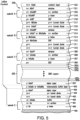
- the doping profile of the emitter and base layers may be illustrated in FIG. 3 , which depicts the amount of doping in the emitter region and the base region of a subcell.
- N-type dopants include silicon, selenium, sulfur, germanium or tin.
- P-type dopants include silicon, zinc, chromium, or germanium.
- one or more of the subcells have a base region having a gradation in doping that increases from a value in the range of 1 x 10 15 to 1 x 10 18 free carriers per cubic centimeter adjacent the p-n junction to a value in the range of 1 x 10 16 to 4 x 10 18 free carriers per cubic centimeter adjacent to the adjoining layer at the rear of the base, and an emitter region having a gradation in doping that decreases from a value in the range of approximately 5 x 10 18 to 1 x 10 17 free carriers per cubic centimeter in the region immediately adjacent the adjoining layer to a value in the range of 5 x 10 15 to 1 x 10 18 free carriers per cubic centimeter in the region adjacent to the p-n junction.
- the heavy lines 612 and 613 shown in Figure 3 illustrates one embodiment of the base doping having an exponential gradation, and the emitter doping being linear.
- the doping level throughout the thickness of the base layer may be exponentially graded from the range of 1 x 10 16 free carriers per cubic centimeter to 1 x 10 18 free carriers per cubic centimeter, as represented by the curve 613 depicted in the Figure.
- the doping level throughout the thickness of the emitter layer may decline linearly from 5 x 10 18 free carriers per cubic centimeter to 5 x 10 17 free carriers per cubic centimeter as represented by the curve 612 depicted in the Figure.
- the exponential doping profile taught by one embodiment of the present disclosure produces a constant field in the doped region.
- the bottom subcell has the smallest short circuit current among all the subcells. Since in a multijunction solar cell, the individual subcells are stacked and form a series circuit, the total current flow in the entire solar cell is therefore limited by the smallest current produced in any of the subcells. Thus, by increasing the short circuit current in the bottom cell, the current more closely approximates that of the higher subcells, and the overall efficiency of the solar cell is increased as well. In a multijunction solar cell with approximately efficiency, the implementation of the present doping arrangement would thereby increase efficiency. In addition to an increase in efficiency, the collection field created by the exponential doping profile will enhance the radiation hardness of the solar cell, which is important for spacecraft applications.
- the exponentially doped profile is the doping design which has been implemented and verified, other doping profiles may give rise to a linear varying collection field which may offer yet other advantages.
- another doping profile may produce a linear field in the doped region which would be advantageous for both minority carrier collection and for radiation hardness at the end-of-life (EOL) of the solar cell.
- EOL end-of-life
- FIG. 4A is a cross-sectional view of a second example of a four junction solar cell 400, which is not part of the invention, after several stages of fabrication including the growth of certain semiconductor layers on the growth substrate up to the contact layer 322, with various subcells being similar to the structure described and depicted in FIG. 2 .
- layers 350, 300 to 304, and 306 through 322 will not be repeated here.
- an intermediate graded interlayer 505, comprising in one example step-graded sublayers 505a through 505z, is disposed over the tunnel diode layer 304.
- the graded interlayer provides a transition in lattice constant from the lattice constant of the substrate to the larger lattice constant of the third and upper subcells.
- a first "alpha" or threading dislocation inhibition layer 504 is deposited over the tunnel diode 303/304, to a thickness of from 0.10 to about 1.0 micron.
- Such an alpha layer is intended to prevent threading dislocations from propagating, either opposite to the direction of growth into the bottom fourth subcell D, or in the direction of growth into the third subcell C, and is more particularly described in U.S. Patent Application Pub. No. 2009/0078309 A1 (Cornfeld et al. ). More generally, the alpha layer has a different composition than the adjacent layers above and below it. As shown in FIG. 4A , the stepped line to the left depicts the step grading of the in plane lattice constant being incrementally greater from sublayer 505a through sublayer 505z, such sublayers being fully relaxed.
- a metamorphic layer (or graded interlayer) 505 is deposited over the alpha layer 504 using a surfactant.
- Layer 505 is preferably a compositionally step-graded series of p-type InGaAs or InGaAlAs layers, preferably with monotonically changing lattice constant, so as to achieve a gradual transition in lattice constant in the semiconductor structure from fourth subcell D to third subcell C while minimizing threading dislocations from occurring.
- the band gap of layer 505 is constant throughout its thickness, preferably approximately equal to 1.22 to 1.34 eV, or otherwise consistent with a value slightly greater than the band gap of the third subcell C.
- the band gap of the sublayers of layer 505 vary in the range of 1.22 to 1.34 eV, with the first layer having a relatively high band gap, and subsequent layers incrementally lower band gaps.
- One example of the graded interlayer may also be expressed as being composed of In x Ga 1-x As, with 0 ⁇ x ⁇ 1, 0 ⁇ y ⁇ 1, and x and y selected such that the band gap of the interlayer remains constant at approximately 1.22 to 1.34 eV or other appropriate band gap.
- aluminum is added to one sublayer to make one particular sublayer harder than another, thereby forcing dislocations in the softer material.
- a suitable chemical element is introduced into the reactor during the growth of layer 505 to improve the surface characteristics of the layer.
- such element may be a dopant or donor atom such as selenium (Se) or tellurium (Te). Small amounts of Se or Te are therefore incorporated in the metamorphic layer 406, and remain in the finished solar cell.
- Se or Te are the preferred n-type dopant atoms, other non-isoelectronic surfactants may be used as well.
- Surfactant assisted growth results in a much smoother or planarized surface. Since the surface topography affects the bulk properties of the semiconductor material as it grows and the layer becomes thicker, the use of the surfactants minimizes threading dislocations in the active regions, and therefore improves overall solar cell efficiency.
- isoelectronic refers to surfactants such as antimony (Sb) or bismuth (Bi), since such elements have the same number of valence electrons as the P atom of InGaP, or the As atom in InGaAlAs, in the metamorphic buffer layer.
- Sb or Bi surfactants will not typically be incorporated into the metamorphic layer 505.
- the metamorphic layer 505 is composed of a plurality of layers of InGaAs, with monotonically changing lattice constant, each layer having a band gap in the range of 1.22 to 1.34 eV.
- the band gap is constant in the range of 1.27 to 1.31 eV through the thickness of layer 505.
- the constant band gap is in the range of 1.28 to 1.29 eV.
- the described example of the present disclosure utilizes a plurality of layers of InGaAs for the metamorphic layer 505 for reasons of manufacturability and radiation transparency
- other examples of the present disclosure may utilize different material systems to achieve a change in lattice constant from third subcell C to fourth subcell D.
- Other embodiments of the present disclosure may utilize continuously graded, as opposed to step graded, materials.
- the graded interlayer may be composed of any of the As, P, N, Sb based III - V compound semiconductors subject to the constraints of having the in-plane lattice parameter less than or equal to that of the third subcell C and greater than or equal to that of the fourth subcell D.
- layer 505 has a band gap energy greater than that of the third subcell C, and in other embodiments has a band gap energy level less than that of the third subcell C.
- Such an alpha layer is intended to prevent threading dislocations from propagating, either opposite to the direction of growth into the fourth subcell D, or in the direction of growth into the third subcell C, and is more particularly described in U.S. Patent Application Pub. No. 2009/0078309 A1 (Cornfeld et al. ).
- an intermediate graded interlayer 505 comprising in one example step-graded sublayers 505a through 505zz, is disposed over the tunnel diode layer 304.
- the graded interlayer provides a transition in lattice constant from the lattice constant of the substrate to the larger lattice constant of the third and upper subcell C, and differs from that of the example of FIG.
- top or uppermost sublayer 505zz of the graded interlayer 505 is strained or only partially relaxed (unlike the fully relaxed layers below it) since it has a lattice constant which is greater than that of the layer above it, i.e., the alpha layer 506 (should there be a second alpha layer) or the BSF layer 306.
- the alpha layer 506 shoulder there be a second alpha layer
- there is an "overshoot" of the grading layers as depicted on the left hand side of FIG. 4B which shows the step-grading of the lattice constant becoming larger from layer 505a to 505zz.
- FIG. 5 is a cross-sectional view of a fourth example of a four junction solar cell 500, which is not part of the invention, after several stages of fabrication including the growth of certain semiconductor layers on the growth substrate up to the contact layer 322, with various subcells being similar to the structure described and depicted in FIG. 2 , 4A , 4B .
- both an intermediate graded layer and a DBR layer are disposed between third subcell C and fourth subcell D.
- the layers 450, 400 to 404, 504 to 506 and 306 through 322 are substantially similar to that of FIG. 2 and FIG. 4A or 4B and their description need not be repeated here.
- DBR Distributed Bragg reflector
- the DBR layers 305 are then grown adjacent to and over the alpha layer 506 (or the metamorphic buffer layer 505 if layer 506 is not present).
- the DBR layers 305 are arranged so that light can enter and pass through the third solar subcell C and at least a portion of which can be reflected back into the third subcell C by the DBR layers 305.
- the distributed Bragg reflector (DBR) layers 305 are specifically located between the third subcell C and metamorphic layer 505.
- distributed Bragg reflector (DBR) layers 305 can be composed of a plurality of alternating layers 305a through 305z of lattice matched materials with discontinuities in their respective indices of refraction.
- the difference in refractive indices between alternating layers is maximized in order to minimize the number of periods required to achieve a given reflectivity, and the thickness and refractive index of each period determines the stop band and its limiting wavelength.
- distributed Bragg reflector (DBR) layers 305a through 305z includes a first DBR layer composed of a plurality of p type In z Al x Ga 1-x-z As layers, and a second DBR layer disposed over the first DBR layer and composed of a plurality of p type In w Al y Ga 1-y-w As layers, where 0 ⁇ w ⁇ 1, 0 ⁇ x ⁇ 1, 0 ⁇ y ⁇ 1, 0 ⁇ z ⁇ 1 and y is greater than x.
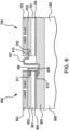
- FIG. 6 is a cross-sectional view of a portion of the solar cell assembly according to the present disclosure as mounted on a panel or supporting substrate, with the Figure depicting two adjacent solar cells 601 and 701 and corresponding CICs 600 and 700 respectively.
- the solar cell 601, 701 includes a coverglass 603, 703 respectively over the semiconductor device to provide radiation resistant shielding from particles in the space environment which could damage the semiconductor material.
- the cover glass 603, 703 is typically a ceria doped borosilicate glass which is typically from three to six mils in thickness and attached by a transparent adhesive 602, 702 respectively to the corresponding solar cell 601, 701.
- Bonding pads of a first and second polarity type are provided on each solar cell.
- a back metal 604 and 704 respectively form contacts of a first polarity type.
- a metal contact 705 is provided along one edge of the solar cell form a contact of the second polarity.
- a plurality of electrical interconnects 607 each composed of a strip of silver-plated nickel-cobalt ferrous alloy material are provided, each interconnect being welded to a respective bonding pad 612 and 705 on each solar cell assembly to electrically connect the adjacent solar cell assemblies of the array in a series electrical circuit.
- An aluminum honeycomb panel 606 having a carbon composite face sheet 605 with a coefficient of thermal expansion (CTE) that substantially matches the germanium of the fourth solar subcell in each solar cell is provided with each CIC 600, 700 or solar cell assembly mounted thereon.
- CTE coefficient of thermal expansion
- the cover glasses 603, 703 each have a metal wrap-around clip 608 depicted in CIC 600 which makes contact with the surface of the cover glass 603, and extends down the gap or space along the side of the solar cell assembly 600 between CICs 600 and 700 to make electrical contact with the metal bonding pad 612 on the back surface of CIC 600, which in turn makes contact with electrical ground.
- the clip 608 grounds the electrical charge build-up on the surface of the cover glass 603 to the ground of the panel or spacecraft.
- Other configurations of grounding techniques for the surface(s) of the coverglass 603, 703 are within the scope of this disclosure.
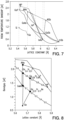
- FIG. 7 is a graph representing the band gap of certain binary materials and their lattice constants.
- the band gap and lattice constants of ternary materials are located on the lines drawn between typical associated binary materials (such as the ternary material AlGaAs being located between the GaAs and AlAs points on the graph, with the band gap of the ternary material lying between 1.42 eV for GaAs and 2.16 eV for AlAs depending upon the relative amount of the individual constituents).
- typical associated binary materials such as the ternary material AlGaAs being located between the GaAs and AlAs points on the graph, with the band gap of the ternary material lying between 1.42 eV for GaAs and 2.16 eV for AlAs depending upon the relative amount of the individual constituents.
- the material constituents of ternary materials can be appropriately selected for growth.
- FIG. 8 is an enlargement of a portion of the graph of FIG. 7 illustrating different compounds of GaInAs and GaInP with different proportions of gallium and indium, and the location of specific compounds on the graph.
- the present disclosure provides a multijunction solar cell that follows a design rule that one should incorporate as many high band gap subcells as possible to achieve the goal to increase the efficiency at high temperature EOL.
- high band gap subcells may retain a greater percentage of cell voltage as temperature increases, thereby offering lower power loss as temperature increases.
- both HT-BOL and HT-EOL performance of the exemplary multijunction solar cell, according to the present disclosure may be expected to be greater than traditional cells.
- the cell efficiency (%) measured at room temperature (RT) 28° C and high temperature (HT) 70° C, at beginning of life (BOL) and end of life (EOL), for a standard three junction commercial solar cell (ZTJ), is shown in Table 1: TABLE 1 CONDITION EFFICIENCY BOL 28° C 29.1% BOL 70° C 26.4% EOL 70° C 23.4% After 5E14 e/cm 2 radiation EOL 70°C 22.0% After 1E15 e/cm 2 radiation
- the solar cell described in the earliest applications of Applicant has a slightly higher cell efficiency than the standard commercial solar cell (ZTJ) at BOL at 70° C.
- the solar cell described in one embodiment of the disclosure exhibits substantially improved cell efficiency (%) over the standard commercial solar cell (ZTJ) at 1 MeV electron equivalent fluence of 5 x 10 14 e/cm 2 , and dramatically improved cell efficiency (%) over the standard commercial solar cell (ZTJ) at 1 MeV electron equivalent fluence of 1 x 10 15 e/cm 2 .
- a low earth orbit (LEO) satellite will typically experience radiation equivalent to 5 x 10 14 electron fluence per square centimeter (hereinafter written as "5E14 e/cm 2 ”) over a five year lifetime.
- a geosynchronous earth orbit (GEO) satellite will typically experience radiation in the range of 5 x 10 14 e/cm 2 to 1 x 10 15 e/cm 2 over a fifteen year lifetime.
- Embodiment 1 Band Gap Composition Subcell A 2.1 AlInGaP Subcell B 1.73 InGaP/AlInGaAs or AlinGaAs/AlInGaAs Subcell C 1.41 (In)GaAs Subcell D 0.67 Ge Efficiency at 70° C after 5E14 e/cm 2 radiation: 24.5% Efficiency at 70° C after 1E15 e/cm 2 radiation: 23.5%
- the exemplary solar cell described herein may require the use of aluminum in the semiconductor composition of each of the top two subcells.
- Aluminum incorporation is widely known in the III-V compound semiconductor industry to degrade BOL subcell performance due to deep level donor defects, higher doping compensation, shorter minority carrier lifetimes, and lower cell voltage and an increased BOL Eg/q - Voc metric.
- increased BOL Eg/q - Voc may be the most problematic shortcoming of aluminum containing subcells; the other limitations can be mitigated by modifying the doping schedule or thinning base thicknesses.
- Example 1 A method for fabricating a four-junction space-qualified solar cell (200, 400, 450, 500) designed for operation at AM0 and at a 1 MeV electron equivalent fluence of at least 1 x 10¹⁴ e/cm2, the solar cell comprising solar subcells (A,B,C,D), comprising the following steps: providing a semiconductor growth substrate (300); forming a fourth solar subcell (D) over or in the growth substrate (300); growing a sequence of layers of semiconductor material using a deposition process to form a solar cell comprising a plurality of solar subcells including a third solar subcell (C) disposed over the fourth solar subcell (D) and being lattice mis-matched from the fourth solar subcell (D), a second solar subcell (B) disposed over and lattice matched to the third solar subcell (C) and having a band gap in the range of approximately 1.55 to 1.8 eV and an upper first solar subcell (A) disposed over and lattice matched to the second solar
- Example 2 The method as defined in Example 1, wherein the upper first solar subcell (A) has a band gap of less than 2.15, the second solar subcell (B) has a band gap of less than 1.73 eV; and the third solar subcell (C) has a band gap in the range of 1.15 to 1.2 eV.
- Example 3 The method as defined in Example 1, wherein the upper first solar subcell (A) has a band gap of 2.05 eV.
- Example 4 The method as defined in Example 1, wherein the band gap of the third solar subcell (C) is less than 1.41 eV, and greater than that of the fourth solar subcell (D).
- Example 5 The method as defined in Example 1, wherein the upper first solar subcell (A) is composed of a base layer (319) of (InxGa1-x)1-yAlyP where x is 0.505, and y is 0.142, corresponding to a band gap of 2.10 eV, and an emitter layer (320) of (InxGa1-x)-yAlyP where x is 0.505, and y is 0.107, corresponding to a band gap of 2.05 eV.
- the upper first solar subcell (A) is composed of a base layer (319) of (InxGa1-x)1-yAlyP where x is 0.505, and y is 0.142, corresponding to a band gap of 2.10 eV
- Example 6 The method as defined in Example 1, further providing an intermediate graded layer (505) disposed between the third solar subcell (C) and the fourth solar subcell (D) wherein the intermediate graded layer (505) is compositionally graded to lattice match the third solar subcell (C) on one side and the fourth solar subcell (D) on the other side and is composed of any of the As, P, N, Sb based III-V compound semiconductors subject to the constraints of having the in-plane lattice parameter greater than or equal to that of the fourth solar subcell (D) and less than or equal to that of the lower third solar subcell (C), and having a band gap energy greater than that of the third solar subcell (C).
- the intermediate graded layer (505) is compositionally graded to lattice match the third solar subcell (C) on one side and the fourth solar subcell (D) on the other side and is composed of any of the As, P, N, Sb based III-V compound semiconductors subject to the constraints of having the in-plane la
- Example 7 The method as defined in Example 1, further providing an intermediate graded layer (505) disposed between the third solar subcell (C) and the fourth solar subcell (D) wherein the inter ⁇ mediate graded layer (505) is compositionally step-graded with between one and four steps to lattice match the third solar subcell (C) on one side and composed of InGaAs or (InxGa1-x)yAl1-y As with 0 ⁇ x ⁇ 1, 0 ⁇ y ⁇ 1, and x and y selected such that the band gap remains in the range of 1.15 to 1.41 eV throughout its thickness.
- the inter ⁇ mediate graded layer (505) is compositionally step-graded with between one and four steps to lattice match the third solar subcell (C) on one side and composed of InGaAs or (InxGa1-x)yAl1-y As with 0 ⁇ x ⁇ 1, 0 ⁇ y ⁇ 1, and x and y selected such that the band gap
- Example 8 The method as defined in Example 6, wherein the intermediate graded layer (505) has a band gap in the range of 1.15 to 1.41 eV, or 1.2 to 1.35 eV, or 1.25 to 1.30 eV.
- Example 9 The method as defined in Example 1, wherein either (i) the emitter layer (320); or (ii) the base layer (319) and emitter layer (320), of the upper first solar subcell (A) have different lattice constants from the lattice constant of the second solar subcell (B).
- Example 10 The method as defined in Example 1, further providing: a distributed Bragg reflector (DBR) layer (305) adjacent to and beneath the third solar subcell (C) and arranged so that light can enter and pass through the third solar subcell (C) and at least a portion of which can be reflected back into the third solar subcell (C) by the DBR layer, wherein the distributed Bragg reflector layer (305) is composed of a plurality of alternating layers of lattice matched materials with discontinuities in their respective indices of refraction, wherein the difference in refractive indices between alternating layers is maximized in order to minimize the number of periods required to achieve a given reflectivity, and the thickness and refractive index of each period determines the stop band and its limiting wavelength, and wherein the DBR layer (305) includes a first DBR layer composed of a plurality of p type AlxGa1-xAs sublayers, and a second DBR layer disposed over the first DBR layer and composed of a plurality of p type AlyG
- each solar subcell (A,B,C) includes an emitter region (320, 314,308) and a base region (319,313, 307), and one or more of the solar subcells have a base region having a gradation in doping that increases exponentially from 1 x 10¹⁵ atoms per cubic centimeter adjacent the p-n junction to 4 x 10¹⁸ atoms per cubic centimeter adjacent to the adjoining layer at the rear of the base, and an emitter region having a gradation in doping that decreases from approximately 5 x 10¹⁸ per cubic centimeter in the region immediately adjacent the adjoining layer to 5 x 10¹⁷ per cubic centimeter in the region adjacent to the p-n junction.
- Example 12 The method as defined in Example 6, wherein the intermediate graded layer (505) is compositionally graded such that sublayers (505a, ... 505zz) are defined having step-graded lattice constants, wherein at least one of the upper sublayers (505zz) of the intermediate graded layer (505) has a larger lattice constant than the adjacent layers (506, 306) to the upper sublayer disposed above the intermediate graded layer.
- Example 13 The method as defined in Example 1, wherein the difference in lattice constant between the adjacent third (C) and fourth (D) solar subcells is in the range of 0.1 to 0.2 Angstroms.
- Example 14 The method as defined in Example 1, further comprising a first threading dislocation inhibition layer (504) having a thickness in the range of 0.1 to 1.0 microns and disposed over said fourth solar subcell (D).
- Example 15 The method as defined in Example 14, further providing a second threading dislocation inhibition layer (506) having a thickness in the range of 0.1 to 1.0 micron and composed of InGa(Al)P, the second threading dislocation inhibition layer (506) being disposed over and directly adjacent to said intermediate graded layer (505) for reducing the propagation of threading dislocations, said second threading dislocation inhibition layer (506) having a composition different from a composition of the first threading dislocation inhibition layer (504).
- a second threading dislocation inhibition layer (506) having a thickness in the range of 0.1 to 1.0 micron and composed of InGa(Al)P, the second threading dislocation inhibition layer (506) being disposed over and directly adjacent to said intermediate graded layer (505) for reducing the propagation of threading dislocations, said second threading dislocation inhibition layer (506) having a composition different from a composition of the first threading dislocation inhibition layer (504).
Landscapes
- Photovoltaic Devices (AREA)
Claims (7)
- Weltraumtaugliche Vierfach-Solarzelle (500), die für den Betrieb bei AM0 und bei einer 1 MeV-Elektronenäquivalent-Fluenz von mindestens 1 x 10¹⁴ e/cm2 konstruiert ist, wobei die Solarzelle Folgendes umfasst: eine Vielzahl von Unterzellen, wobei eine Kombination von Zusammensetzungen und Bandlücken der Unterzellen zur Maximierung der Effizienz der Solarzelle (500) bei einer vorbestimmten Zeit nach Einführung, wenn die Solarzelle (500) im Weltraum bei AM0 und bei einer Betriebstemperatur in dem Bereich von 40 bis 70 Grad Celsius eingesetzt wird, konstruiert ist, wobei die vorbestimmte Zeit mindestens fünf Jahre beträgt und als das Lebensdauerende (EOL) bezeichnet wird, wobei die Solarzelle (500) Folgendes umfasst:obere erste Solarunterzelle (A), die aus Indium-Gallium-Aluminiumphosphid besteht und eine erste Bandlücke aufweist, wobei die erste Bandlücke gleich 2,03 eV beträgt, an ein Glasträgerelement mit einem transparenten Haftmittel angebracht ist;eine zweite Solarunterzelle (B), die an die erste Solarunterzelle (A) angrenzt und Folgendes einschließt: eine Emitterschicht (314), die aus Indium-Galliumphosphid oder Aluminium-Indium-Galliumarsenid besteht, und eine Basisschicht (313), die aus Aluminium-Indium-Galliumarsenid besteht, und eine zweite Bandlücke aufweist, die gleich 1,55 beträgt, und mit der oberen ersten Solarunterzelle (A) gitterangepasst ist, wobei die Emitter- (314) und Basisschicht (313) der zweiten Solarunterzelle (B) einen photoelektrischen Übergang bilden;eine dritte Solarunterzelle (C), die an die zweite Solarunterzelle (B) angrenzt und aus Indium-Galliumarsenid besteht, eine dritte Bandlücke aufweist, die kleiner ist als die zweite Bandlücke, und mit der zweiten Solarunterzelle gitterangepasst ist, wobei die dritte Bandlücke gleich 1,2 eV beträgt;eine vierte Solarunterzelle (D), die an die dritte Solarunterzelle (C) angrenzt und davon gitterfehlangepasst ist und aus Germanium besteht, eine vierte Bandlücke von ungefähr 0,67 eV aufweist, undeine Schicht von verteiltem Bragg-Reflektor (DBR) (305), angrenzend an und zwischen der dritten (C) und der vierten (D) Solarunterzelle und derart angeordnet ist, dass Licht in die dritte Solarunterzelle (C) eintreten und hindurchgehen kann und zumindest ein Teil davon in die dritte Solarunterzelle durch die DBR-Schicht zurückreflektiert werden kann.
- Solarzelle (500) wie in Anspruch 1 definiert, wobei die vierte Solarunterzelle (D) von der dritten Solarunterzelle (C) gitterfehlangepasst ist und wobei der Unterschied in der Gitterkonstante zwischen der angrenzenden dritten Solarunterzelle (C) und vierten Solarunterzelle (D) bevorzugt in dem Bereich von 0,1 bis 0,2 Angström liegt.
- Solarzelle (500) wie in einem der vorstehenden Ansprüche definiert, wobei die Schicht von verteiltem Bragg-Reflektor (305) aus einer Vielzahl von abwechselnden Schichten von gitterangepassten Materialien mit Unregelmäßigkeiten in ihren jeweiligen Brechungsindizes besteht und der Unterschied in den Brechungsindizes zwischen abwechselnden Schichten maximiert wird, um die Anzahl von Zeiträumen zu minimieren, die zum Erreichen einer gegebenen Reflexionsfähigkeit erforderlich sind, und die Dicke und der Brechungsindex von jedem Zeitraum das Sperrband und seine Grenzwellenlänge bestimmen.
- Solarzelle (500) wie in einem der vorstehenden Ansprüche definiert, wobei die DBR-Schicht (305) Folgendes einschließt: eine erste DBR-Schicht, die aus einer Vielzahl von p-leitenden InzAlxGa1-x-zAs-Schichten besteht, und eine zweite DBR-Schicht, die über der ersten DBR-Schicht angeordnet ist und aus einer Vielzahl von p-leitenden InwAlyGa1-y-xAs-Schichten besteht, wo 0 < x < 1, 0 < y < 1, 0 < z < 1 und y größer ist als x, sodass sich die erste und zweite DBR-Schicht in der Zusammensetzung unterscheiden, wodurch die Reflexionsbandbreite der DBR-Schicht (305) zunimmt.
- Solarzelle (500) wie in einem der vorstehenden Ansprüche definiert, wo jede Solarunterzelle (A, B, C, D) einen Emitterbereich (320, 314, 308) und einen Basisbereich (319, 313, 307) einschließt und eine oder mehrere der Solarunterzellen Folgendes aufweisen: einen Basisbereich, der eine Abstufung der Dotierung aufweist, die exponentiell von 1 x 10¹⁵ Atome pro Kubikzentimeter, angrenzend an den p-n-Übergang, bis 4 x 10¹⁸ Atome pro Kubikzentimeter, angrenzend an die angrenzende Schicht an der Rückseite der Basis, zunimmt, und einen Emitterbereich, der eine Abstufung der Dotierung aufweist, die von ungefähr 5 x 10¹⁸ Atome pro Kubikzentimeter in dem Bereich, unmittelbar angrenzend an die angrenzende Schicht, bis 5 x 10¹⁷ Atome pro Kubikzentimeter, angrenzend an den p-n-Übergang, abnimmt.
- Solarzelle (500) wie in einem der vorstehenden Ansprüche definiert, die weiter eine erste Fadenversetzungsinhibierungsschicht (504) umfasst, die eine Dicke in dem Bereich von 0,1 bis 1,0 Mikron aufweist und über der vierten Solarunterzelle (D) angeordnet ist.
- Solarzelle (500) wie in Anspruch 6 definiert, die weiter eine zweite Fadenversetzungsinhibierungsschicht (507) umfasst, die eine Dicke in dem Bereich von 0,1 bis 1,0 Mikron aufweist und aus InGa(Al)P besteht, wobei die zweite Fadenversetzungsinhibierungsschicht (507) über der abgestuften Zwischenschicht (506) angeordnet ist und direkt daran angrenzt, für die Reduzierung der Propagation von Fadenversetzungen, wobei die zweite Fadenversetzungsinhibierungsschicht (507) eine Zusammensetzung aufweist, die sich von einer Zusammensetzung der ersten Fadenversetzungsinhibierungsschicht (504) unterscheidet.
Priority Applications (1)
| Application Number | Priority Date | Filing Date | Title |
|---|---|---|---|
| EP22160040.6A EP4036992B1 (de) | 2018-01-17 | 2018-01-17 | Solarzelle mit vierfachabzweigung und solarzellenanordnungen für raumfahrtanwendungen |
Applications Claiming Priority (3)
| Application Number | Priority Date | Filing Date | Title |
|---|---|---|---|
| EP21187462.3A EP3923349B1 (de) | 2018-01-17 | 2018-01-17 | Solarzelle mit vierfachabzweigung und solarzellenanordnungen für raumfahrtanwendungen |
| EP18152179.0A EP3514838B1 (de) | 2018-01-17 | 2018-01-17 | Solarzelle mit vierfachabzweigung und solarzellenanordnungen für raumfahrtanwendungen |
| EP22160040.6A EP4036992B1 (de) | 2018-01-17 | 2018-01-17 | Solarzelle mit vierfachabzweigung und solarzellenanordnungen für raumfahrtanwendungen |
Related Parent Applications (3)
| Application Number | Title | Priority Date | Filing Date |
|---|---|---|---|
| EP21187462.3A Division-Into EP3923349B1 (de) | 2018-01-17 | 2018-01-17 | Solarzelle mit vierfachabzweigung und solarzellenanordnungen für raumfahrtanwendungen |
| EP21187462.3A Division EP3923349B1 (de) | 2018-01-17 | 2018-01-17 | Solarzelle mit vierfachabzweigung und solarzellenanordnungen für raumfahrtanwendungen |
| EP18152179.0A Division EP3514838B1 (de) | 2018-01-17 | 2018-01-17 | Solarzelle mit vierfachabzweigung und solarzellenanordnungen für raumfahrtanwendungen |
Publications (2)
| Publication Number | Publication Date |
|---|---|
| EP4036992A1 EP4036992A1 (de) | 2022-08-03 |
| EP4036992B1 true EP4036992B1 (de) | 2025-04-02 |
Family
ID=61002924
Family Applications (4)
| Application Number | Title | Priority Date | Filing Date |
|---|---|---|---|
| EP22160040.6A Active EP4036992B1 (de) | 2018-01-17 | 2018-01-17 | Solarzelle mit vierfachabzweigung und solarzellenanordnungen für raumfahrtanwendungen |
| EP23186134.5A Withdrawn EP4250375A3 (de) | 2018-01-17 | 2018-01-17 | Solarzelle mit vier anschlüssen und solarzellenanordnungen für raumanwendungen |
| EP21187462.3A Active EP3923349B1 (de) | 2018-01-17 | 2018-01-17 | Solarzelle mit vierfachabzweigung und solarzellenanordnungen für raumfahrtanwendungen |
| EP18152179.0A Revoked EP3514838B1 (de) | 2018-01-17 | 2018-01-17 | Solarzelle mit vierfachabzweigung und solarzellenanordnungen für raumfahrtanwendungen |
Family Applications After (3)
| Application Number | Title | Priority Date | Filing Date |
|---|---|---|---|
| EP23186134.5A Withdrawn EP4250375A3 (de) | 2018-01-17 | 2018-01-17 | Solarzelle mit vier anschlüssen und solarzellenanordnungen für raumanwendungen |
| EP21187462.3A Active EP3923349B1 (de) | 2018-01-17 | 2018-01-17 | Solarzelle mit vierfachabzweigung und solarzellenanordnungen für raumfahrtanwendungen |
| EP18152179.0A Revoked EP3514838B1 (de) | 2018-01-17 | 2018-01-17 | Solarzelle mit vierfachabzweigung und solarzellenanordnungen für raumfahrtanwendungen |
Country Status (1)
| Country | Link |
|---|---|
| EP (4) | EP4036992B1 (de) |
Families Citing this family (6)
| Publication number | Priority date | Publication date | Assignee | Title |
|---|---|---|---|---|
| EP3876291A1 (de) * | 2020-03-06 | 2021-09-08 | SolAero Technologies Corp., a corporation of the state of Delaware | Verteilte bragg-reflektorstrukturen in mehrfachübergangssolarzellen |
| US11362230B1 (en) | 2021-01-28 | 2022-06-14 | Solaero Technologies Corp. | Multijunction solar cells |
| EP4092762A1 (de) * | 2021-05-18 | 2022-11-23 | SolAero Technologies Corp., a corporation of the state of Delaware | Mehrfachsolarzellen |
| EP4092763A1 (de) * | 2021-05-18 | 2022-11-23 | SolAero Technologies Corp., a corporation of the state of Delaware | Mehrfachsolarzellen |
| EP4235817A1 (de) * | 2022-02-28 | 2023-08-30 | SolAero Technologies Corp., a corporation of the state of Delaware | Metamorphe solarzellen mit mehreren übergängen |
| CN118676238B (zh) * | 2024-07-19 | 2025-03-21 | 江苏仲磊芯半导体有限公司 | 一种抗辐照五结太阳能电池及其制作方法 |
Citations (17)
| Publication number | Priority date | Publication date | Assignee | Title |
|---|---|---|---|---|
| US4881979A (en) | 1984-08-29 | 1989-11-21 | Varian Associates, Inc. | Junctions for monolithic cascade solar cells and methods |
| US6660928B1 (en) | 2002-04-02 | 2003-12-09 | Essential Research, Inc. | Multi-junction photovoltaic cell |
| WO2004022820A1 (en) | 2002-09-05 | 2004-03-18 | Midwest Research Institute | Method for achieving device-quality, lattice- mismatched, heteroepitaxial active layers |
| US20060144435A1 (en) | 2002-05-21 | 2006-07-06 | Wanlass Mark W | High-efficiency, monolithic, multi-bandgap, tandem photovoltaic energy converters |
| US20090229659A1 (en) | 2002-05-21 | 2009-09-17 | Midwest Research Institute | Monolithic, multi-bandgap, tandem, ultra-thin, strain-counterbalanced, photovoltaic energy converters with optimal subcell bandgaps |
| EP2148378A1 (de) | 2008-07-25 | 2010-01-27 | Emcore Solar Power, Inc. | Sperrschichten in umgekehrten metamorphischen Multiverbindungssolarzellen |
| US20100147366A1 (en) | 2008-12-17 | 2010-06-17 | Emcore Solar Power, Inc. | Inverted Metamorphic Multijunction Solar Cells with Distributed Bragg Reflector |
| EP2264788A2 (de) | 2005-01-04 | 2010-12-22 | AZUR SPACE Solar Power GmbH | Monolithische Mehrfach-Solarzelle |
| US20120211068A1 (en) | 2007-09-24 | 2012-08-23 | Emcore Solar Power, Inc. | Inverted metamorphic multijunction solar cell with two metamorphic layers and homojunction top cell |
| EP2610924A1 (de) | 2011-12-27 | 2013-07-03 | Emcore Solar Power, Inc. | Invertierte metamorphe Solarzelle mit mehreren Übergängen mit metamorphen Schichten und mit oberer Zelle mit Homoübergang |
| US20140076401A1 (en) | 2012-09-14 | 2014-03-20 | The Boeing Company | GROUP-IV SOLAR CELL STRUCTURE USING GROUP-IV or III-V HETEROSTRUCTURES |
| US20140182667A1 (en) | 2013-01-03 | 2014-07-03 | Benjamin C. Richards | Multijunction solar cell with low band gap absorbing layer in the middle cell |
| EP2779253A1 (de) | 2013-03-14 | 2014-09-17 | The Boeing Company | Solarzellenstrukturen für verbesserte Stromerzeugung und Sammlung |
| US9018521B1 (en) | 2008-12-17 | 2015-04-28 | Solaero Technologies Corp. | Inverted metamorphic multijunction solar cell with DBR layer adjacent to the top subcell |
| EP3159942A1 (de) | 2015-10-19 | 2017-04-26 | SolAero Technologies Corp. | Metamorphe mehrfachsolarzellenanordnung für raumfahrtanwendungen |
| EP3159943A1 (de) | 2015-10-19 | 2017-04-26 | SolAero Technologies Corp. | Metamorphische mehrfachsolarzelle für raumfahrtanwendungen |
| EP3133650B1 (de) | 2015-08-17 | 2020-09-23 | SolAero Technologies Corp. | Solarzelle mit vierfachabzweigung für raumfahrtanwendungen |
Family Cites Families (13)
| Publication number | Priority date | Publication date | Assignee | Title |
|---|---|---|---|---|
| US4667059A (en) | 1985-10-22 | 1987-05-19 | The United States Of America As Represented By The United States Department Of Energy | Current and lattice matched tandem solar cell |
| US4902468A (en) | 1987-10-21 | 1990-02-20 | Westinghouse Electric Corp. | Control rod support having planar wear surfaces |
| JPH03159943A (ja) | 1989-11-17 | 1991-07-09 | Nitto Boseki Co Ltd | 人工大理石用材料 |
| US20090078309A1 (en) | 2007-09-24 | 2009-03-26 | Emcore Corporation | Barrier Layers In Inverted Metamorphic Multijunction Solar Cells |
| US20100122724A1 (en) | 2008-11-14 | 2010-05-20 | Emcore Solar Power, Inc. | Four Junction Inverted Metamorphic Multijunction Solar Cell with Two Metamorphic Layers |
| US20130139877A1 (en) * | 2007-09-24 | 2013-06-06 | Emcore Solar Power, Inc. | Inverted metamorphic multijunction solar cell with gradation in doping in the window layer |
| WO2013074530A2 (en) | 2011-11-15 | 2013-05-23 | Solar Junction Corporation | High efficiency multijunction solar cells |
| DE102012004734A1 (de) * | 2012-03-08 | 2013-09-12 | Fraunhofer-Gesellschaft zur Förderung der angewandten Forschung e.V. | Mehrfachsolarzelle und deren Verwendung |
| US9853180B2 (en) | 2013-06-19 | 2017-12-26 | Solaero Technologies Corp. | Inverted metamorphic multijunction solar cell with surface passivation |
| KR102364160B1 (ko) | 2014-03-06 | 2022-02-21 | 서울반도체 주식회사 | Mjt led를 이용한 백라이트 모듈 및 이를 포함하는 백라이트 유닛 |
| ES2749215T3 (es) | 2014-03-13 | 2020-03-19 | Azur Space Solar Power Gmbh | Célula solar múltiple |
| US9954128B2 (en) * | 2016-01-12 | 2018-04-24 | The Boeing Company | Structures for increased current generation and collection in solar cells with low absorptance and/or low diffusion length |
| KR102001335B1 (ko) | 2018-01-19 | 2019-07-17 | 엘지전자 주식회사 | 윤활유 공급장치 및 이를 적용한 압축기 |
-
2018
- 2018-01-17 EP EP22160040.6A patent/EP4036992B1/de active Active
- 2018-01-17 EP EP23186134.5A patent/EP4250375A3/de not_active Withdrawn
- 2018-01-17 EP EP21187462.3A patent/EP3923349B1/de active Active
- 2018-01-17 EP EP18152179.0A patent/EP3514838B1/de not_active Revoked
Patent Citations (17)
| Publication number | Priority date | Publication date | Assignee | Title |
|---|---|---|---|---|
| US4881979A (en) | 1984-08-29 | 1989-11-21 | Varian Associates, Inc. | Junctions for monolithic cascade solar cells and methods |
| US6660928B1 (en) | 2002-04-02 | 2003-12-09 | Essential Research, Inc. | Multi-junction photovoltaic cell |
| US20060144435A1 (en) | 2002-05-21 | 2006-07-06 | Wanlass Mark W | High-efficiency, monolithic, multi-bandgap, tandem photovoltaic energy converters |
| US20090229659A1 (en) | 2002-05-21 | 2009-09-17 | Midwest Research Institute | Monolithic, multi-bandgap, tandem, ultra-thin, strain-counterbalanced, photovoltaic energy converters with optimal subcell bandgaps |
| WO2004022820A1 (en) | 2002-09-05 | 2004-03-18 | Midwest Research Institute | Method for achieving device-quality, lattice- mismatched, heteroepitaxial active layers |
| EP2264788A2 (de) | 2005-01-04 | 2010-12-22 | AZUR SPACE Solar Power GmbH | Monolithische Mehrfach-Solarzelle |
| US20120211068A1 (en) | 2007-09-24 | 2012-08-23 | Emcore Solar Power, Inc. | Inverted metamorphic multijunction solar cell with two metamorphic layers and homojunction top cell |
| EP2148378A1 (de) | 2008-07-25 | 2010-01-27 | Emcore Solar Power, Inc. | Sperrschichten in umgekehrten metamorphischen Multiverbindungssolarzellen |
| US20100147366A1 (en) | 2008-12-17 | 2010-06-17 | Emcore Solar Power, Inc. | Inverted Metamorphic Multijunction Solar Cells with Distributed Bragg Reflector |
| US9018521B1 (en) | 2008-12-17 | 2015-04-28 | Solaero Technologies Corp. | Inverted metamorphic multijunction solar cell with DBR layer adjacent to the top subcell |
| EP2610924A1 (de) | 2011-12-27 | 2013-07-03 | Emcore Solar Power, Inc. | Invertierte metamorphe Solarzelle mit mehreren Übergängen mit metamorphen Schichten und mit oberer Zelle mit Homoübergang |
| US20140076401A1 (en) | 2012-09-14 | 2014-03-20 | The Boeing Company | GROUP-IV SOLAR CELL STRUCTURE USING GROUP-IV or III-V HETEROSTRUCTURES |
| US20140182667A1 (en) | 2013-01-03 | 2014-07-03 | Benjamin C. Richards | Multijunction solar cell with low band gap absorbing layer in the middle cell |
| EP2779253A1 (de) | 2013-03-14 | 2014-09-17 | The Boeing Company | Solarzellenstrukturen für verbesserte Stromerzeugung und Sammlung |
| EP3133650B1 (de) | 2015-08-17 | 2020-09-23 | SolAero Technologies Corp. | Solarzelle mit vierfachabzweigung für raumfahrtanwendungen |
| EP3159942A1 (de) | 2015-10-19 | 2017-04-26 | SolAero Technologies Corp. | Metamorphe mehrfachsolarzellenanordnung für raumfahrtanwendungen |
| EP3159943A1 (de) | 2015-10-19 | 2017-04-26 | SolAero Technologies Corp. | Metamorphische mehrfachsolarzelle für raumfahrtanwendungen |
Non-Patent Citations (24)
| Title |
|---|
| "Doctoral Disseratation, Universität Konstanz", 20 July 2007, article BAUR CARSTEN: "Entwicklung und Charakterisierung von III-V Weltraumsolarzellen", XP093357154 |
| AGUI T., TAKAMOTO T., KANEIWA M.: "Investigation on AlInGaP solar cells for current matched multijunction cells", PROCEEDINGS OF THE 3RD WORLD CONFERENCE ON PHOTOVOLTAIC ENERGY CONVERSION : JOINT CONFERENCE OF 13TH PV SCIENCE & ENGINEERING CONFERENCE, 30TH IEEE PV SPECIALISTS CONFERENCE, 18TH EUROPEAN PV SOLAR ENERGY CONFERENCE; OSAKA INTERNATIONAL CONGRESS CENT, vol. 1, 1 January 2003 (2003-01-01), JP , pages 670 - 672, XP093357150, ISBN: 978-4-9901816-0-4 |
| D16a - King, "BAND-GAP-ENGINEERED ARCHITECTURES FOR HIGHEFFICIENCY MULTIJUNCTION CONCENTRATOR SOLAR CELLS " Konferenz, 2009 |
| DIMROTH F, ET AL.: "NEXT GENERATION GaInP/GaInAs/Ge MULTI-JUNCTION SPACE SOLAR CELLS", 17TH. E.C. PHOTOVOLTAIC SOLAR ENERGY CONFERENCE. MUNICH, GERMANY, OCT. 22 - 26, 2001., MUNICH : WIP-RENEWABLE ENERGIES., DE, vol. CONF. 17., 22 October 2001 (2001-10-22), DE , pages 2150 - 2154, XP001139903, ISBN: 978-3-936338-08-9 |
| FUHRMANN D., ET AL.: "ABOUT 42%-CLASS CPV CELLS AND PATHWAYS BEYOND", CPV, vol. 9, 1 January 2013 (2013-01-01), pages 1 - 26, XP055827485 |
| GUDOVSKIKH A. S., ET AL.: "Anisotype GaAs Based Heterojunctions for III-V Multijunction Solar Cells", 25TH EUROPEAN PHOTOVOLTAIC SOLAR ENERGY CONFERENCE AND EXHIBITION / 5TH WORLD CONFERENCE ON PHOTOVOLTAIC ENERGY CONVERSION, VALENCIA, SPAIN, 6 September 2010 (2010-09-06), Valencia, Spain , pages 1 - 10, XP055827483 |
| HECKELMANN S, LACKNER D, KARCHER C, BETT A W, , , : "Investigations on A- xGai_xAs Solar Cells Grown by MOVPE", IEEE2014,2156-3381, vol. 5, no. 1, 1 January 2015 (2015-01-01), pages 445 - 453, XP093212585 |
| HECTOR COTAL, FETZER CHRIS, BOISVERT JOSEPH, KINSEY GEOFFREY, KING RICHARD, HEBERT PETER, YOON HOJUN, KARAM NASSER: "III–V multijunction solar cells for concentrating photovoltaics", ENERGY & ENVIRONMENTAL SCIENCE, vol. 2, no. 2, 1 January 2009 (2009-01-01), pages 174, XP055033873, ISSN: 17545692, DOI: 10.1039/B809257E |
| JAN SCHÖNE: "Kontrolle von Spannungsrelaxation und Defektbildung in metamorphen III-V Halbleiterheterostrukturen für hocheffiziente Solarzellen", DISSERTATION, 21 July 2009 (2009-07-21), pages 1 - 146, XP055528372, Retrieved from the Internet <URL:https://d-nb.info/1019870907/34> |
| KING R. R, BOCA A, HONG W, LIU X. -Q, BHUSARI D, LARRABEE D, EDMONDSON K. M, LAW D. C, FETZER C. M, MESROPIAN S, KARAM N. H: "Band-Gap-Engineered Architectures for High-Efficiency Multijunction Concentrator Solar Cells", THE COMPILED STATE-OF-THE-ART OF PV SOLAR TECHNOLOGY AND DEPLOYMENT : 24TH EUROPEAN PHOTOVOLTAIC SOLAR ENERGY CONFERENCE AND EXHIBITION ; CONFERENCE 21 - 25 SEPTEMBER 2009, EXHIBITION 21 - 24 SEPTEMBER 2009, HAMBURG ; PROCEEDINGS ; EU PVSEC, WIP-RENE, 21 September 2009 (2009-09-21) - 2009-09-25, Munich , pages 1 - 33, XP055779663, ISBN: 978-3-936338-25-6, DOI: 10.4229/24theupvsec2009-1ao.5.2 |
| KING R. R.: "Band gap-voltage offset and energy production in next- generation multijunction solar cells", PROG. PHOTOVOLT: RES. APPL., vol. 19, 1 January 2011 (2011-01-01), pages 797 - 812, XP055827492 |
| KING R., ET AL.: "Band gap-voltage offset and energy production in next-generation multijunction solar cells", EU PVSEC PROCEEDINGS : 25 TH EUROPEAN PHOTOVOLTAIC SOLAR ENERGY CONFERENCE AND EXHIBITION / 5 TH WORLD CONFERENCE ON PHOTOVOLTAIC ENERGY CONVERSION, 6 September 2010 (2010-09-06), pages 1 - 14, XP055827498 |
| KLINGER VERA: "Entwicklung von ultradünnen metamorphen Mehrfachsolarzellen zum Erreichen höchster Umwandlungseffizienzen", DISSERTATION, UNIVERSITÄT KONSTANZ, 1 January 2013 (2013-01-01), Universität Konstanz, XP055947596, Retrieved from the Internet <URL:https://www.reiner-lemoine-stiftung.de/en/pdf/dissertationen/Dissertation-Vera_Klinger.pdf> |
| LE DONNE, A. ; ACCIARRI, M. ; GORI, G. ; COLLETTO, R. ; CAMPESATO, R. ; BINETTI, S.: "Optical and electrical characterization of AlGaInP solar cells", SOLAR ENERGY MATERIALS AND SOLAR CELLS, ELSEVIER SCIENCE PUBLISHERS, AMSTERDAM., NL, vol. 94, no. 12, 1 December 2010 (2010-12-01), NL , pages 2002 - 2006, XP027383816, ISSN: 0927-0248 |
| MEUSEL M, ET AL.: "European Roadmap for the Development of III-V Multi-Junction Space Solar Cells", PROCEEDINGS OF THE EUROPEAN PHOTOVOLTAIC SOLAR ENERGY CONFERENCE, XX, XX, 7 June 2004 (2004-06-07) - 11 June 2004 (2004-06-11), XX , pages 3581 - 3586, XP002369931 |
| PERL EMMETT E.; SIMON JOHN; GEISZ JOHN F.; OLAVARRIA WALDO; YOUNG MICHELLE; DUDA ANNA; FRIEDMAN DANIEL J.; STEINER MYLES A.: "Development of High-Bandgap AlGaInP Solar Cells Grown by Organometallic Vapor-Phase Epitaxy", IEEE JOURNAL OF PHOTOVOLTAICS, IEEE, vol. 6, no. 3, 1 May 2016 (2016-05-01), pages 770 - 776, XP011607124, ISSN: 2156-3381, DOI: 10.1109/JPHOTOV.2016.2537543 |
| R CAMPESATO, GORI G, CASALE M, GABETTA G: "High Efficiency Four Junction Lattice Matched Solar Cells for Space Applications: Analysis of Radiation Hardness Against 1 MeV Electrons", PROCEEDINGS OF THE 29TH EUROPEAN PHOTOVOLTAIC SOLAR ENERGY CONFERENCE AND EXHIBITION, WIP-RENEWABLE ENERGIES, SYLVENSTEINSTR. 2 81369 MUNICH, GERMANY, 25 September 2014 (2014-09-25), Sylvensteinstr. 2 81369 Munich, Germany , XP055548202, ISBN: 978-3-936338-34-8, DOI: 10.4229/EUPVSEC20142014-4DO.13.3 |
| R. CAMPESATO ; M. CASALE ; G. GORI ; G. GABETTA ; R. COLLETTO ; S. TAYLOR: "High efficiency solar cells based on AlInGaP", PHOTOVOLTAIC SPECIALISTS CONFERENCE (PVSC), 2009 34TH IEEE, IEEE, PISCATAWAY, NJ, USA, 7 June 2009 (2009-06-07), Piscataway, NJ, USA , pages 001112 - 001117, XP031626502, ISBN: 978-1-4244-2949-3 |
| R. R. KING: "Group-IV Subcells in Multijunction Concentrator Solar Cells", ECS MEETING ABSTRACTS, ABSTRACT #3130, HONOLULU PRIME 2012, © 2012 THE ELECTROCHEMICAL SOCIETY, 1 March 2012 (2012-03-01), XP055685198, Retrieved from the Internet <URL:https://iopscience.iop.org/article/10.1149/MA2012-02/43/3130/pdf> DOI: 10.1149/05009.0287ecst |
| RICHARD R KING: "Raising the Efficiency Ceiling in Multijunction Solar Cells", 14 September 2009 (2009-09-14), XP055221989, Retrieved from the Internet <URL:http://www.spectrolab.com/DataSheets/PV/pv_tech/msce.pdf> |
| ROBERTA CAMPESATO, GABRIELE GORI, ERMINIO GRECO, ANDREA SCACCABAROZZI, SIMONA BINETTI, ALESSIA LE DONNE: "High efficiency AlInGaP and AlInGaAs Solar Cells for 32% four junction devices", EU PVSEC 2013, 28TH EUROPEAN PHOTOVOLTAIC SOLAR ENERGY CONFERENCE AND EXHIBITION, PARC DES EXPOSITIONS PARIS NORD VILLEPINTE, PARIS, FRANCE, CONFERENCE 30 SEPTEMBER - 04 OCTOBER 2013, EXHIBITION 1- 3 OCTOBER 2013 : THE MOST INSPIRING PLATFORM FOR THE, 1 January 2013 (2013-01-01) - 2013-10-04, pages 63 - 68, XP055827499, ISBN: 3-936338-33-7 |
| STAN M A, ET AL.: "THE DEVELOPMENT OF >28% EFFICIENT TRIPLE-JUNCTION SPACE SOLAR CELLS AT EMCORE PHOTOVOLTAICS", PROCEEDINGS OF THE 3RD WORLD CONFERENCE ON PHOTOVOLTAIC ENERGY CONVERSION : JOINT CONFERENCE OF 13TH PV SCIENCE & ENGINEERING CONFERENCE, 30TH IEEE PV SPECIALISTS CONFERENCE, 18TH EUROPEAN PV SOLAR ENERGY CONFERENCE; OSAKA INTERNATIONAL CONGRESS CENT, vol. 01, 11 May 2003 (2003-05-11), JP , pages 662 - 665, XP008053707, ISBN: 978-4-9901816-0-4 |
| STROBL, ET AL: "About AZUR'S "3G30-advanced" Space Solar Cell and Next Generation Product with 35% Efficiency", PROCEEDINGS/EU PVSEC 2012, 27TH EUROPEAN PHOTOVOLTAIC SOLAR ENERGY CONFERENCE AND EXHIBITION: MESSE FRANKFURT AND AND CONGRESS CENTER, FRANKFURT, GERMANY, CONFERENCE 24 - 28 SEPTEMBER 2012, EXHIBITION 25 - 28 SEPTEMBER 2012, WIP RENEWABLE ENERGIES, 24 September 2012 (2012-09-24) - 2012-09-28, pages 104 - 108, XP055501334, ISBN: 3-936338-28-0, DOI: 10.4229/27thEUPVSEC2012-1BO.10.3 |
| TOBIAS ROESENER: "Hocheffiziente III-V-Mehrfachsolarzellen auf Silicium Substrat", DISSERTATION, UNIVERSITÄT KONSTANZ, 1 January 2013 (2013-01-01), XP055155900, Retrieved from the Internet <URL:http://www.reiner-lemoine-stiftung.de/pdf/dissertationen/dissertation_roesener.pdf> |
Also Published As
| Publication number | Publication date |
|---|---|
| EP3514838B1 (de) | 2021-09-01 |
| EP3923349B1 (de) | 2023-07-19 |
| EP3514838A1 (de) | 2019-07-24 |
| EP4250375A2 (de) | 2023-09-27 |
| EP4250375A3 (de) | 2023-11-01 |
| EP4036992A1 (de) | 2022-08-03 |
| EP3923349A1 (de) | 2021-12-15 |
Similar Documents
| Publication | Publication Date | Title |
|---|---|---|
| EP4036992B1 (de) | Solarzelle mit vierfachabzweigung und solarzellenanordnungen für raumfahrtanwendungen | |
| US20180240922A1 (en) | Four junction solar cell and solar cell assemblies for space applications | |
| EP3159940B1 (de) | Metamorphe mehrfachsolarzellenanordnung für raumfahrtanwendungen | |
| US20200027999A1 (en) | Multijunction solar cell and solar cell assemblies for space applications | |
| US20150357501A1 (en) | Four junction inverted metamorphic solar cell | |
| EP3159942B1 (de) | Metamorphe mehrfachsolarzellenanordnung für raumfahrtanwendungen | |
| US20170062642A1 (en) | Inverted metamorphic multijunction solar cell | |
| US20200274016A1 (en) | MULTIJUNCTION SOLAR CELLS ON BULK GeSi SUBSTRATE | |
| CN110047954B (zh) | 用于空间应用的四结太阳能电池 | |
| EP3159943B1 (de) | Metamorphische mehrfachsolarzelle für raumfahrtanwendungen | |
| US11145776B2 (en) | Multijunction metamorphic solar cell for space applications | |
| EP3301727B1 (de) | Gitterangepasste mehrfachsolarzellenanordnungen für raumfahrtanwendungen und herstellungsverfahren dafür | |
| US11742452B2 (en) | Inverted metamorphic multijunction solar cell | |
| EP3091583B1 (de) | Invertierte metamorphe solarzelle mit mehreren übergängen | |
| US12211948B1 (en) | Multijunction solar cells | |
| US20220320358A1 (en) | Multijunction solar cells with shifted junction | |
| US20180226532A1 (en) | METHOD FOR FABRICATING MULTIJUNCTION SOLAR CELLS ON BULK GeSi SUBSTRATE | |
| EP4235817A1 (de) | Metamorphe solarzellen mit mehreren übergängen | |
| RU2755630C2 (ru) | Солнечный элемент с четырьмя переходами для космических применений | |
| US20250081658A1 (en) | Method of designing four junction metamorphic multijunction solar cells for space applications | |
| EP4243090A1 (de) | Metamorphe solarzellen mit vier übergängen für raumanwendungen | |
| US20220393055A1 (en) | Multijunction metamorphic solar cells | |
| US20230142352A1 (en) | Inverted metamorphic multijunction solar cells for space applications | |
| US20220102564A1 (en) | Four junction metamorphic multijunction solar cells for space applications | |
| EP4170732A1 (de) | Metamorphe solarzelle mit mehreren übergängen |
Legal Events
| Date | Code | Title | Description |
|---|---|---|---|
| PUAI | Public reference made under article 153(3) epc to a published international application that has entered the european phase |
Free format text: ORIGINAL CODE: 0009012 |
|
| STAA | Information on the status of an ep patent application or granted ep patent |
Free format text: STATUS: THE APPLICATION HAS BEEN PUBLISHED |
|
| AC | Divisional application: reference to earlier application |
Ref document number: 3514838 Country of ref document: EP Kind code of ref document: P Ref document number: 3923349 Country of ref document: EP Kind code of ref document: P |
|
| AK | Designated contracting states |
Kind code of ref document: A1 Designated state(s): AL AT BE BG CH CY CZ DE DK EE ES FI FR GB GR HR HU IE IS IT LI LT LU LV MC MK MT NL NO PL PT RO RS SE SI SK SM TR |
|
| STAA | Information on the status of an ep patent application or granted ep patent |
Free format text: STATUS: REQUEST FOR EXAMINATION WAS MADE |
|
| 17P | Request for examination filed |
Effective date: 20230202 |
|
| RBV | Designated contracting states (corrected) |
Designated state(s): AL AT BE BG CH CY CZ DE DK EE ES FI FR GB GR HR HU IE IS IT LI LT LU LV MC MK MT NL NO PL PT RO RS SE SI SK SM TR |
|
| STAA | Information on the status of an ep patent application or granted ep patent |
Free format text: STATUS: EXAMINATION IS IN PROGRESS |
|
| 17Q | First examination report despatched |
Effective date: 20230609 |
|
| TPAC | Observations filed by third parties |
Free format text: ORIGINAL CODE: EPIDOSNTIPA |
|
| GRAP | Despatch of communication of intention to grant a patent |
Free format text: ORIGINAL CODE: EPIDOSNIGR1 |
|
| STAA | Information on the status of an ep patent application or granted ep patent |
Free format text: STATUS: GRANT OF PATENT IS INTENDED |
|
| INTG | Intention to grant announced |
Effective date: 20241024 |
|
| GRAS | Grant fee paid |
Free format text: ORIGINAL CODE: EPIDOSNIGR3 |
|
| GRAA | (expected) grant |
Free format text: ORIGINAL CODE: 0009210 |
|
| STAA | Information on the status of an ep patent application or granted ep patent |
Free format text: STATUS: THE PATENT HAS BEEN GRANTED |
|
| AC | Divisional application: reference to earlier application |
Ref document number: 3514838 Country of ref document: EP Kind code of ref document: P Ref document number: 3923349 Country of ref document: EP Kind code of ref document: P |
|
| AK | Designated contracting states |
Kind code of ref document: B1 Designated state(s): AL AT BE BG CH CY CZ DE DK EE ES FI FR GB GR HR HU IE IS IT LI LT LU LV MC MK MT NL NO PL PT RO RS SE SI SK SM TR |
|
| REG | Reference to a national code |
Ref country code: GB Ref legal event code: FG4D |
|
| REG | Reference to a national code |
Ref country code: IE Ref legal event code: FG4D |
|
| REG | Reference to a national code |
Ref country code: DE Ref legal event code: R096 Ref document number: 602018080866 Country of ref document: DE |
|
| REG | Reference to a national code |
Ref country code: NL Ref legal event code: MP Effective date: 20250402 |
|
| PG25 | Lapsed in a contracting state [announced via postgrant information from national office to epo] |
Ref country code: NL Free format text: LAPSE BECAUSE OF FAILURE TO SUBMIT A TRANSLATION OF THE DESCRIPTION OR TO PAY THE FEE WITHIN THE PRESCRIBED TIME-LIMIT Effective date: 20250402 |
|
| REG | Reference to a national code |
Ref country code: AT Ref legal event code: MK05 Ref document number: 1782199 Country of ref document: AT Kind code of ref document: T Effective date: 20250402 |
|
| PG25 | Lapsed in a contracting state [announced via postgrant information from national office to epo] |
Ref country code: PT Free format text: LAPSE BECAUSE OF FAILURE TO SUBMIT A TRANSLATION OF THE DESCRIPTION OR TO PAY THE FEE WITHIN THE PRESCRIBED TIME-LIMIT Effective date: 20250804 Ref country code: FI Free format text: LAPSE BECAUSE OF FAILURE TO SUBMIT A TRANSLATION OF THE DESCRIPTION OR TO PAY THE FEE WITHIN THE PRESCRIBED TIME-LIMIT Effective date: 20250402 Ref country code: ES Free format text: LAPSE BECAUSE OF FAILURE TO SUBMIT A TRANSLATION OF THE DESCRIPTION OR TO PAY THE FEE WITHIN THE PRESCRIBED TIME-LIMIT Effective date: 20250402 |
|
| REG | Reference to a national code |
Ref country code: LT Ref legal event code: MG9D |
|
| PG25 | Lapsed in a contracting state [announced via postgrant information from national office to epo] |
Ref country code: NO Free format text: LAPSE BECAUSE OF FAILURE TO SUBMIT A TRANSLATION OF THE DESCRIPTION OR TO PAY THE FEE WITHIN THE PRESCRIBED TIME-LIMIT Effective date: 20250702 Ref country code: GR Free format text: LAPSE BECAUSE OF FAILURE TO SUBMIT A TRANSLATION OF THE DESCRIPTION OR TO PAY THE FEE WITHIN THE PRESCRIBED TIME-LIMIT Effective date: 20250703 |
|
| PG25 | Lapsed in a contracting state [announced via postgrant information from national office to epo] |
Ref country code: PL Free format text: LAPSE BECAUSE OF FAILURE TO SUBMIT A TRANSLATION OF THE DESCRIPTION OR TO PAY THE FEE WITHIN THE PRESCRIBED TIME-LIMIT Effective date: 20250402 |
|
| PG25 | Lapsed in a contracting state [announced via postgrant information from national office to epo] |
Ref country code: BG Free format text: LAPSE BECAUSE OF FAILURE TO SUBMIT A TRANSLATION OF THE DESCRIPTION OR TO PAY THE FEE WITHIN THE PRESCRIBED TIME-LIMIT Effective date: 20250402 |
|
| PG25 | Lapsed in a contracting state [announced via postgrant information from national office to epo] |
Ref country code: HR Free format text: LAPSE BECAUSE OF FAILURE TO SUBMIT A TRANSLATION OF THE DESCRIPTION OR TO PAY THE FEE WITHIN THE PRESCRIBED TIME-LIMIT Effective date: 20250402 |
|
| PG25 | Lapsed in a contracting state [announced via postgrant information from national office to epo] |
Ref country code: AT Free format text: LAPSE BECAUSE OF FAILURE TO SUBMIT A TRANSLATION OF THE DESCRIPTION OR TO PAY THE FEE WITHIN THE PRESCRIBED TIME-LIMIT Effective date: 20250402 |
|
| PG25 | Lapsed in a contracting state [announced via postgrant information from national office to epo] |
Ref country code: RS Free format text: LAPSE BECAUSE OF FAILURE TO SUBMIT A TRANSLATION OF THE DESCRIPTION OR TO PAY THE FEE WITHIN THE PRESCRIBED TIME-LIMIT Effective date: 20250702 |
|
| PG25 | Lapsed in a contracting state [announced via postgrant information from national office to epo] |
Ref country code: IS Free format text: LAPSE BECAUSE OF FAILURE TO SUBMIT A TRANSLATION OF THE DESCRIPTION OR TO PAY THE FEE WITHIN THE PRESCRIBED TIME-LIMIT Effective date: 20250802 |
|
| PG25 | Lapsed in a contracting state [announced via postgrant information from national office to epo] |
Ref country code: LV Free format text: LAPSE BECAUSE OF FAILURE TO SUBMIT A TRANSLATION OF THE DESCRIPTION OR TO PAY THE FEE WITHIN THE PRESCRIBED TIME-LIMIT Effective date: 20250402 |
|
| REG | Reference to a national code |
Ref country code: DE Ref legal event code: R026 Ref document number: 602018080866 Country of ref document: DE |
|
| PLBI | Opposition filed |
Free format text: ORIGINAL CODE: 0009260 |
|
| PG25 | Lapsed in a contracting state [announced via postgrant information from national office to epo] |
Ref country code: DK Free format text: LAPSE BECAUSE OF FAILURE TO SUBMIT A TRANSLATION OF THE DESCRIPTION OR TO PAY THE FEE WITHIN THE PRESCRIBED TIME-LIMIT Effective date: 20250402 Ref country code: SM Free format text: LAPSE BECAUSE OF FAILURE TO SUBMIT A TRANSLATION OF THE DESCRIPTION OR TO PAY THE FEE WITHIN THE PRESCRIBED TIME-LIMIT Effective date: 20250402 |
|
| REG | Reference to a national code |
Ref country code: CH Ref legal event code: L10 Free format text: ST27 STATUS EVENT CODE: U-0-0-L10-L00 (AS PROVIDED BY THE NATIONAL OFFICE) Effective date: 20260114 |
|
| PGFP | Annual fee paid to national office [announced via postgrant information from national office to epo] |
Ref country code: FR Payment date: 20251208 Year of fee payment: 9 |
|
| PLAX | Notice of opposition and request to file observation + time limit sent |
Free format text: ORIGINAL CODE: EPIDOSNOBS2 |
|
| PG25 | Lapsed in a contracting state [announced via postgrant information from national office to epo] |
Ref country code: CZ Free format text: LAPSE BECAUSE OF FAILURE TO SUBMIT A TRANSLATION OF THE DESCRIPTION OR TO PAY THE FEE WITHIN THE PRESCRIBED TIME-LIMIT Effective date: 20250402 |
|
| PG25 | Lapsed in a contracting state [announced via postgrant information from national office to epo] |
Ref country code: EE Free format text: LAPSE BECAUSE OF FAILURE TO SUBMIT A TRANSLATION OF THE DESCRIPTION OR TO PAY THE FEE WITHIN THE PRESCRIBED TIME-LIMIT Effective date: 20250402 |
|
| PG25 | Lapsed in a contracting state [announced via postgrant information from national office to epo] |
Ref country code: SK Free format text: LAPSE BECAUSE OF FAILURE TO SUBMIT A TRANSLATION OF THE DESCRIPTION OR TO PAY THE FEE WITHIN THE PRESCRIBED TIME-LIMIT Effective date: 20250402 |
|
| PG25 | Lapsed in a contracting state [announced via postgrant information from national office to epo] |
Ref country code: IT Free format text: LAPSE BECAUSE OF FAILURE TO SUBMIT A TRANSLATION OF THE DESCRIPTION OR TO PAY THE FEE WITHIN THE PRESCRIBED TIME-LIMIT Effective date: 20250402 |
|
| 26 | Opposition filed |
Opponent name: AZUR SPACE SOLAR POWER GMBH Effective date: 20260102 |