EP3876291A1 - Verteilte bragg-reflektorstrukturen in mehrfachübergangssolarzellen - Google Patents
Verteilte bragg-reflektorstrukturen in mehrfachübergangssolarzellen Download PDFInfo
- Publication number
- EP3876291A1 EP3876291A1 EP20161374.2A EP20161374A EP3876291A1 EP 3876291 A1 EP3876291 A1 EP 3876291A1 EP 20161374 A EP20161374 A EP 20161374A EP 3876291 A1 EP3876291 A1 EP 3876291A1
- Authority
- EP
- European Patent Office
- Prior art keywords
- subcell
- dbr
- solar cell
- layers
- layer
- Prior art date
- Legal status (The legal status is an assumption and is not a legal conclusion. Google has not performed a legal analysis and makes no representation as to the accuracy of the status listed.)
- Pending
Links
- 239000004065 semiconductor Substances 0.000 claims abstract description 67
- 239000000463 material Substances 0.000 claims abstract description 55
- 238000004519 manufacturing process Methods 0.000 claims abstract description 26
- 230000003595 spectral effect Effects 0.000 claims description 29
- 229910000530 Gallium indium arsenide Inorganic materials 0.000 claims description 24
- 239000000758 substrate Substances 0.000 claims description 22
- 229910052738 indium Inorganic materials 0.000 claims description 16
- APFVFJFRJDLVQX-UHFFFAOYSA-N indium atom Chemical compound [In] APFVFJFRJDLVQX-UHFFFAOYSA-N 0.000 claims description 15
- 239000000969 carrier Substances 0.000 claims description 12
- FTWRSWRBSVXQPI-UHFFFAOYSA-N alumanylidynearsane;gallanylidynearsane Chemical compound [As]#[Al].[As]#[Ga] FTWRSWRBSVXQPI-UHFFFAOYSA-N 0.000 claims description 9
- 229910052732 germanium Inorganic materials 0.000 claims description 9
- GNPVGFCGXDBREM-UHFFFAOYSA-N germanium atom Chemical compound [Ge] GNPVGFCGXDBREM-UHFFFAOYSA-N 0.000 claims description 9
- GYHNNYVSQQEPJS-UHFFFAOYSA-N Gallium Chemical compound [Ga] GYHNNYVSQQEPJS-UHFFFAOYSA-N 0.000 claims description 8
- 229910052733 gallium Inorganic materials 0.000 claims description 8
- IHGSAQHSAGRWNI-UHFFFAOYSA-N 1-(4-bromophenyl)-2,2,2-trifluoroethanone Chemical compound FC(F)(F)C(=O)C1=CC=C(Br)C=C1 IHGSAQHSAGRWNI-UHFFFAOYSA-N 0.000 claims description 5
- 229910005540 GaP Inorganic materials 0.000 claims description 5
- KXNLCSXBJCPWGL-UHFFFAOYSA-N [Ga].[As].[In] Chemical compound [Ga].[As].[In] KXNLCSXBJCPWGL-UHFFFAOYSA-N 0.000 claims description 5
- HZXMRANICFIONG-UHFFFAOYSA-N gallium phosphide Chemical compound [Ga]#P HZXMRANICFIONG-UHFFFAOYSA-N 0.000 claims description 5
- 230000007423 decrease Effects 0.000 claims description 4
- 238000010521 absorption reaction Methods 0.000 claims description 3
- 229910052782 aluminium Inorganic materials 0.000 abstract description 5
- XAGFODPZIPBFFR-UHFFFAOYSA-N aluminium Chemical compound [Al] XAGFODPZIPBFFR-UHFFFAOYSA-N 0.000 abstract description 5
- 239000010410 layer Substances 0.000 description 208
- 210000004027 cell Anatomy 0.000 description 131
- 238000000034 method Methods 0.000 description 27
- 239000000203 mixture Substances 0.000 description 22
- 230000008569 process Effects 0.000 description 21
- 238000013461 design Methods 0.000 description 17
- 150000001875 compounds Chemical class 0.000 description 16
- 238000000151 deposition Methods 0.000 description 8
- JBRZTFJDHDCESZ-UHFFFAOYSA-N AsGa Chemical compound [As]#[Ga] JBRZTFJDHDCESZ-UHFFFAOYSA-N 0.000 description 7
- 229910001218 Gallium arsenide Inorganic materials 0.000 description 7
- 238000006243 chemical reaction Methods 0.000 description 7
- 239000002019 doping agent Substances 0.000 description 7
- XUIMIQQOPSSXEZ-UHFFFAOYSA-N Silicon Chemical compound [Si] XUIMIQQOPSSXEZ-UHFFFAOYSA-N 0.000 description 6
- 229910052751 metal Inorganic materials 0.000 description 6
- 239000002184 metal Substances 0.000 description 6
- 229910052710 silicon Inorganic materials 0.000 description 6
- 239000010703 silicon Substances 0.000 description 6
- 239000000126 substance Substances 0.000 description 6
- 238000000862 absorption spectrum Methods 0.000 description 5
- 239000000470 constituent Substances 0.000 description 5
- 230000000694 effects Effects 0.000 description 5
- 238000005516 engineering process Methods 0.000 description 5
- 230000005855 radiation Effects 0.000 description 5
- 230000008021 deposition Effects 0.000 description 4
- 238000001451 molecular beam epitaxy Methods 0.000 description 4
- 230000003287 optical effect Effects 0.000 description 4
- 230000006798 recombination Effects 0.000 description 4
- 238000005215 recombination Methods 0.000 description 4
- 206010011906 Death Diseases 0.000 description 3
- 230000015572 biosynthetic process Effects 0.000 description 3
- 239000013078 crystal Substances 0.000 description 3
- 238000010348 incorporation Methods 0.000 description 3
- 239000011229 interlayer Substances 0.000 description 3
- 238000005259 measurement Methods 0.000 description 3
- 230000006911 nucleation Effects 0.000 description 3
- 238000010899 nucleation Methods 0.000 description 3
- 238000012545 processing Methods 0.000 description 3
- 238000002310 reflectometry Methods 0.000 description 3
- 238000012360 testing method Methods 0.000 description 3
- 230000005641 tunneling Effects 0.000 description 3
- 235000012431 wafers Nutrition 0.000 description 3
- CIWBSHSKHKDKBQ-JLAZNSOCSA-N Ascorbic acid Chemical compound OC[C@H](O)[C@H]1OC(=O)C(O)=C1O CIWBSHSKHKDKBQ-JLAZNSOCSA-N 0.000 description 2
- IJGRMHOSHXDMSA-UHFFFAOYSA-N Atomic nitrogen Chemical compound N#N IJGRMHOSHXDMSA-UHFFFAOYSA-N 0.000 description 2
- AUCDRFABNLOFRE-UHFFFAOYSA-N alumane;indium Chemical compound [AlH3].[In] AUCDRFABNLOFRE-UHFFFAOYSA-N 0.000 description 2
- 230000004888 barrier function Effects 0.000 description 2
- 230000008859 change Effects 0.000 description 2
- 238000005229 chemical vapour deposition Methods 0.000 description 2
- 238000007906 compression Methods 0.000 description 2
- 230000006835 compression Effects 0.000 description 2
- 238000010276 construction Methods 0.000 description 2
- 230000006872 improvement Effects 0.000 description 2
- 238000012986 modification Methods 0.000 description 2
- 230000004048 modification Effects 0.000 description 2
- 238000002161 passivation Methods 0.000 description 2
- 230000000737 periodic effect Effects 0.000 description 2
- 230000007704 transition Effects 0.000 description 2
- ZOXJGFHDIHLPTG-UHFFFAOYSA-N Boron Chemical compound [B] ZOXJGFHDIHLPTG-UHFFFAOYSA-N 0.000 description 1
- VYZAMTAEIAYCRO-UHFFFAOYSA-N Chromium Chemical compound [Cr] VYZAMTAEIAYCRO-UHFFFAOYSA-N 0.000 description 1
- 206010073306 Exposure to radiation Diseases 0.000 description 1
- UFHFLCQGNIYNRP-UHFFFAOYSA-N Hydrogen Chemical compound [H][H] UFHFLCQGNIYNRP-UHFFFAOYSA-N 0.000 description 1
- OAICVXFJPJFONN-UHFFFAOYSA-N Phosphorus Chemical compound [P] OAICVXFJPJFONN-UHFFFAOYSA-N 0.000 description 1
- BUGBHKTXTAQXES-UHFFFAOYSA-N Selenium Chemical compound [Se] BUGBHKTXTAQXES-UHFFFAOYSA-N 0.000 description 1
- NINIDFKCEFEMDL-UHFFFAOYSA-N Sulfur Chemical compound [S] NINIDFKCEFEMDL-UHFFFAOYSA-N 0.000 description 1
- ATJFFYVFTNAWJD-UHFFFAOYSA-N Tin Chemical compound [Sn] ATJFFYVFTNAWJD-UHFFFAOYSA-N 0.000 description 1
- HCHKCACWOHOZIP-UHFFFAOYSA-N Zinc Chemical compound [Zn] HCHKCACWOHOZIP-UHFFFAOYSA-N 0.000 description 1
- 238000002835 absorbance Methods 0.000 description 1
- 230000006978 adaptation Effects 0.000 description 1
- 239000000853 adhesive Substances 0.000 description 1
- 230000001070 adhesive effect Effects 0.000 description 1
- 238000004458 analytical method Methods 0.000 description 1
- 230000003466 anti-cipated effect Effects 0.000 description 1
- 229910052787 antimony Inorganic materials 0.000 description 1
- WATWJIUSRGPENY-UHFFFAOYSA-N antimony atom Chemical compound [Sb] WATWJIUSRGPENY-UHFFFAOYSA-N 0.000 description 1
- 229910052785 arsenic Inorganic materials 0.000 description 1
- RQNWIZPPADIBDY-UHFFFAOYSA-N arsenic atom Chemical compound [As] RQNWIZPPADIBDY-UHFFFAOYSA-N 0.000 description 1
- 229910052797 bismuth Inorganic materials 0.000 description 1
- JCXGWMGPZLAOME-UHFFFAOYSA-N bismuth atom Chemical compound [Bi] JCXGWMGPZLAOME-UHFFFAOYSA-N 0.000 description 1
- 229910052796 boron Inorganic materials 0.000 description 1
- 229910052729 chemical element Inorganic materials 0.000 description 1
- 229910052804 chromium Inorganic materials 0.000 description 1
- 239000011651 chromium Substances 0.000 description 1
- 230000003247 decreasing effect Effects 0.000 description 1
- 230000007547 defect Effects 0.000 description 1
- 230000001419 dependent effect Effects 0.000 description 1
- 238000011161 development Methods 0.000 description 1
- 238000009792 diffusion process Methods 0.000 description 1
- 230000005684 electric field Effects 0.000 description 1
- 230000005611 electricity Effects 0.000 description 1
- 230000008020 evaporation Effects 0.000 description 1
- 238000001704 evaporation Methods 0.000 description 1
- 238000002474 experimental method Methods 0.000 description 1
- 238000009472 formulation Methods 0.000 description 1
- 239000007789 gas Substances 0.000 description 1
- 229910052739 hydrogen Inorganic materials 0.000 description 1
- 239000001257 hydrogen Substances 0.000 description 1
- 238000005286 illumination Methods 0.000 description 1
- 239000012535 impurity Substances 0.000 description 1
- 238000012886 linear function Methods 0.000 description 1
- 229910052757 nitrogen Inorganic materials 0.000 description 1
- 230000005693 optoelectronics Effects 0.000 description 1
- 125000002524 organometallic group Chemical group 0.000 description 1
- 230000037361 pathway Effects 0.000 description 1
- 229910052698 phosphorus Inorganic materials 0.000 description 1
- 239000011574 phosphorus Substances 0.000 description 1
- 238000005289 physical deposition Methods 0.000 description 1
- 239000002243 precursor Substances 0.000 description 1
- 238000003908 quality control method Methods 0.000 description 1
- 238000011160 research Methods 0.000 description 1
- 230000002441 reversible effect Effects 0.000 description 1
- 229910052711 selenium Inorganic materials 0.000 description 1
- 239000011669 selenium Substances 0.000 description 1
- 230000035945 sensitivity Effects 0.000 description 1
- 239000007787 solid Substances 0.000 description 1
- 229910052717 sulfur Inorganic materials 0.000 description 1
- 239000011593 sulfur Substances 0.000 description 1
- 239000013077 target material Substances 0.000 description 1
- 230000002123 temporal effect Effects 0.000 description 1
- 229910052716 thallium Inorganic materials 0.000 description 1
- BKVIYDNLLOSFOA-UHFFFAOYSA-N thallium Chemical compound [Tl] BKVIYDNLLOSFOA-UHFFFAOYSA-N 0.000 description 1
- 229910052718 tin Inorganic materials 0.000 description 1
- 238000007740 vapor deposition Methods 0.000 description 1
- 238000000927 vapour-phase epitaxy Methods 0.000 description 1
- 229910052725 zinc Inorganic materials 0.000 description 1
- 239000011701 zinc Substances 0.000 description 1
Images


Classifications
-
- H—ELECTRICITY
- H01—ELECTRIC ELEMENTS
- H01L—SEMICONDUCTOR DEVICES NOT COVERED BY CLASS H10
- H01L31/00—Semiconductor devices sensitive to infrared radiation, light, electromagnetic radiation of shorter wavelength or corpuscular radiation and specially adapted either for the conversion of the energy of such radiation into electrical energy or for the control of electrical energy by such radiation; Processes or apparatus specially adapted for the manufacture or treatment thereof or of parts thereof; Details thereof
- H01L31/04—Semiconductor devices sensitive to infrared radiation, light, electromagnetic radiation of shorter wavelength or corpuscular radiation and specially adapted either for the conversion of the energy of such radiation into electrical energy or for the control of electrical energy by such radiation; Processes or apparatus specially adapted for the manufacture or treatment thereof or of parts thereof; Details thereof adapted as photovoltaic [PV] conversion devices
- H01L31/06—Semiconductor devices sensitive to infrared radiation, light, electromagnetic radiation of shorter wavelength or corpuscular radiation and specially adapted either for the conversion of the energy of such radiation into electrical energy or for the control of electrical energy by such radiation; Processes or apparatus specially adapted for the manufacture or treatment thereof or of parts thereof; Details thereof adapted as photovoltaic [PV] conversion devices characterised by potential barriers
- H01L31/068—Semiconductor devices sensitive to infrared radiation, light, electromagnetic radiation of shorter wavelength or corpuscular radiation and specially adapted either for the conversion of the energy of such radiation into electrical energy or for the control of electrical energy by such radiation; Processes or apparatus specially adapted for the manufacture or treatment thereof or of parts thereof; Details thereof adapted as photovoltaic [PV] conversion devices characterised by potential barriers the potential barriers being only of the PN homojunction type, e.g. bulk silicon PN homojunction solar cells or thin film polycrystalline silicon PN homojunction solar cells
- H01L31/0687—Multiple junction or tandem solar cells
-
- H—ELECTRICITY
- H01—ELECTRIC ELEMENTS
- H01L—SEMICONDUCTOR DEVICES NOT COVERED BY CLASS H10
- H01L31/00—Semiconductor devices sensitive to infrared radiation, light, electromagnetic radiation of shorter wavelength or corpuscular radiation and specially adapted either for the conversion of the energy of such radiation into electrical energy or for the control of electrical energy by such radiation; Processes or apparatus specially adapted for the manufacture or treatment thereof or of parts thereof; Details thereof
- H01L31/0248—Semiconductor devices sensitive to infrared radiation, light, electromagnetic radiation of shorter wavelength or corpuscular radiation and specially adapted either for the conversion of the energy of such radiation into electrical energy or for the control of electrical energy by such radiation; Processes or apparatus specially adapted for the manufacture or treatment thereof or of parts thereof; Details thereof characterised by their semiconductor bodies
- H01L31/0256—Semiconductor devices sensitive to infrared radiation, light, electromagnetic radiation of shorter wavelength or corpuscular radiation and specially adapted either for the conversion of the energy of such radiation into electrical energy or for the control of electrical energy by such radiation; Processes or apparatus specially adapted for the manufacture or treatment thereof or of parts thereof; Details thereof characterised by their semiconductor bodies characterised by the material
- H01L31/0264—Inorganic materials
- H01L31/0304—Inorganic materials including, apart from doping materials or other impurities, only AIIIBV compounds
- H01L31/03046—Inorganic materials including, apart from doping materials or other impurities, only AIIIBV compounds including ternary or quaternary compounds, e.g. GaAlAs, InGaAs, InGaAsP
-
- H—ELECTRICITY
- H01—ELECTRIC ELEMENTS
- H01L—SEMICONDUCTOR DEVICES NOT COVERED BY CLASS H10
- H01L31/00—Semiconductor devices sensitive to infrared radiation, light, electromagnetic radiation of shorter wavelength or corpuscular radiation and specially adapted either for the conversion of the energy of such radiation into electrical energy or for the control of electrical energy by such radiation; Processes or apparatus specially adapted for the manufacture or treatment thereof or of parts thereof; Details thereof
- H01L31/04—Semiconductor devices sensitive to infrared radiation, light, electromagnetic radiation of shorter wavelength or corpuscular radiation and specially adapted either for the conversion of the energy of such radiation into electrical energy or for the control of electrical energy by such radiation; Processes or apparatus specially adapted for the manufacture or treatment thereof or of parts thereof; Details thereof adapted as photovoltaic [PV] conversion devices
- H01L31/054—Optical elements directly associated or integrated with the PV cell, e.g. light-reflecting means or light-concentrating means
- H01L31/0549—Optical elements directly associated or integrated with the PV cell, e.g. light-reflecting means or light-concentrating means comprising spectrum splitting means, e.g. dichroic mirrors
-
- H—ELECTRICITY
- H01—ELECTRIC ELEMENTS
- H01L—SEMICONDUCTOR DEVICES NOT COVERED BY CLASS H10
- H01L31/00—Semiconductor devices sensitive to infrared radiation, light, electromagnetic radiation of shorter wavelength or corpuscular radiation and specially adapted either for the conversion of the energy of such radiation into electrical energy or for the control of electrical energy by such radiation; Processes or apparatus specially adapted for the manufacture or treatment thereof or of parts thereof; Details thereof
- H01L31/04—Semiconductor devices sensitive to infrared radiation, light, electromagnetic radiation of shorter wavelength or corpuscular radiation and specially adapted either for the conversion of the energy of such radiation into electrical energy or for the control of electrical energy by such radiation; Processes or apparatus specially adapted for the manufacture or treatment thereof or of parts thereof; Details thereof adapted as photovoltaic [PV] conversion devices
- H01L31/06—Semiconductor devices sensitive to infrared radiation, light, electromagnetic radiation of shorter wavelength or corpuscular radiation and specially adapted either for the conversion of the energy of such radiation into electrical energy or for the control of electrical energy by such radiation; Processes or apparatus specially adapted for the manufacture or treatment thereof or of parts thereof; Details thereof adapted as photovoltaic [PV] conversion devices characterised by potential barriers
- H01L31/068—Semiconductor devices sensitive to infrared radiation, light, electromagnetic radiation of shorter wavelength or corpuscular radiation and specially adapted either for the conversion of the energy of such radiation into electrical energy or for the control of electrical energy by such radiation; Processes or apparatus specially adapted for the manufacture or treatment thereof or of parts thereof; Details thereof adapted as photovoltaic [PV] conversion devices characterised by potential barriers the potential barriers being only of the PN homojunction type, e.g. bulk silicon PN homojunction solar cells or thin film polycrystalline silicon PN homojunction solar cells
- H01L31/0687—Multiple junction or tandem solar cells
- H01L31/06875—Multiple junction or tandem solar cells inverted grown metamorphic [IMM] multiple junction solar cells, e.g. III-V compounds inverted metamorphic multi-junction cells
-
- Y—GENERAL TAGGING OF NEW TECHNOLOGICAL DEVELOPMENTS; GENERAL TAGGING OF CROSS-SECTIONAL TECHNOLOGIES SPANNING OVER SEVERAL SECTIONS OF THE IPC; TECHNICAL SUBJECTS COVERED BY FORMER USPC CROSS-REFERENCE ART COLLECTIONS [XRACs] AND DIGESTS
- Y02—TECHNOLOGIES OR APPLICATIONS FOR MITIGATION OR ADAPTATION AGAINST CLIMATE CHANGE
- Y02E—REDUCTION OF GREENHOUSE GAS [GHG] EMISSIONS, RELATED TO ENERGY GENERATION, TRANSMISSION OR DISTRIBUTION
- Y02E10/00—Energy generation through renewable energy sources
- Y02E10/50—Photovoltaic [PV] energy
- Y02E10/52—PV systems with concentrators
-
- Y—GENERAL TAGGING OF NEW TECHNOLOGICAL DEVELOPMENTS; GENERAL TAGGING OF CROSS-SECTIONAL TECHNOLOGIES SPANNING OVER SEVERAL SECTIONS OF THE IPC; TECHNICAL SUBJECTS COVERED BY FORMER USPC CROSS-REFERENCE ART COLLECTIONS [XRACs] AND DIGESTS
- Y02—TECHNOLOGIES OR APPLICATIONS FOR MITIGATION OR ADAPTATION AGAINST CLIMATE CHANGE
- Y02E—REDUCTION OF GREENHOUSE GAS [GHG] EMISSIONS, RELATED TO ENERGY GENERATION, TRANSMISSION OR DISTRIBUTION
- Y02E10/00—Energy generation through renewable energy sources
- Y02E10/50—Photovoltaic [PV] energy
- Y02E10/544—Solar cells from Group III-V materials
-
- Y—GENERAL TAGGING OF NEW TECHNOLOGICAL DEVELOPMENTS; GENERAL TAGGING OF CROSS-SECTIONAL TECHNOLOGIES SPANNING OVER SEVERAL SECTIONS OF THE IPC; TECHNICAL SUBJECTS COVERED BY FORMER USPC CROSS-REFERENCE ART COLLECTIONS [XRACs] AND DIGESTS
- Y02—TECHNOLOGIES OR APPLICATIONS FOR MITIGATION OR ADAPTATION AGAINST CLIMATE CHANGE
- Y02P—CLIMATE CHANGE MITIGATION TECHNOLOGIES IN THE PRODUCTION OR PROCESSING OF GOODS
- Y02P70/00—Climate change mitigation technologies in the production process for final industrial or consumer products
- Y02P70/50—Manufacturing or production processes characterised by the final manufactured product
Definitions
- the present disclosure relates to solar cells and the fabrication of solar cells, and more particularly the design and specification of a lattice matched multijunction solar cells adapted for specific space missions.
- III-V compound semiconductor multijunction solar cells Solar power from photovoltaic cells, also called solar cells, has been predominantly provided by silicon semiconductor technology.
- high-volume manufacturing of III-V compound semiconductor multijunction solar cells for space applications has accelerated the development of such technology not only for use in space but also for terrestrial solar power applications.
- III-V compound semiconductor multijunction devices have greater energy conversion efficiencies and generally more radiation resistance, although they tend to be more complex to properly specify and manufacture.
- Typical commercial III-V compound semiconductor multijunction solar cells have energy efficiencies that exceed 27% under one sun, air mass 0 (AM0) illumination, whereas even the most efficient silicon technologies generally reach only about 18% efficiency under comparable conditions.
- AM0 air mass 0
- III-V compound semiconductor solar cells compared to silicon solar cells is in part based on the ability to achieve spectral splitting of the incident radiation through the use of a plurality of photovoltaic regions with different band gap energies, and accumulating the current from each of the regions.
- the size, mass and cost of a satellite power system are dependent on the power and energy conversion efficiency of the solar cells used.
- the size of the payload and the availability of on-board services are proportional to the amount of power provided.
- the power-to-weight ratio and lifetime efficiency of a solar cell becomes increasingly more important, and there is increasing interest not only the amount of power provided at initial deployment, but over the entire service life of the satellite system, or in terms of a design specification, the amount of power provided at the "end of life" (EOL).
- Typical III-V compound semiconductor solar cells are fabricated on a semiconductor wafer in vertical, multijunction structures or stacked sequence of solar subcells, each subcell formed with appropriate semiconductor layers and including a p-n photoactive junction. Each subcell is designed to convert photons over different spectral or wavelength bands to electrical current. After the sunlight impinges on the front of the solar cell, and photons pass through the subcells, with each subcell being designed for photons in a specific wavelength band. After passing through a subcell, the photons that are not absorbed and converted to electrical energy propagate to the next subcells, where such photons are intended to be captured and converted to electrical energy.
- the energy conversion efficiency of multijunction solar cells is affected by such factors as the number of subcells, the thickness of each subcell, the composition and doping of each active layer in a subcell, and the consequential band structure, electron energy levels, conduction, and absorption of each subcell, as well as the effect of its exposure to radiation in the ambient environment over time.
- the identification and specification of such design parameters is a non-trivial engineering undertaking, and would vary depending upon the specific space mission and customer design requirements. Since the power output is a function of both the voltage and the current produced by a subcell, a simplistic view may seek to maximize both parameters in a subcell by increasing a constituent element, or the doping level, to achieve that effect.
- Another important mechanical or structural consideration in the choice of semiconductor layers for a solar cell is the desirability of the adjacent layers of semiconductor materials in the solar cell, i.e. each layer of crystalline semiconductor material that is deposited and grown to form a solar subcell, have similar crystal lattice constants or parameters.
- the present disclosure provides a multijunction solar cell comprising: a first and a second solar subcell each having an emitter layer and a base layer forming a photoelectric junction; a first distributed Bragg reflector (DBR) structure disposed beneath the base layer of the first solar subcell and composed of a plurality of alternating layers of different semiconductor materials with discontinuities in their respective indices of refraction and arranged so that light can enter and pass through the first solar subcell and at least a first portion of which in a first spectral wavelength range [of 840 to 890 nm] can be reflected back into the first solar subcell by the DBR structure, and a second portion of which in a second spectral wavelength range [of 790 to 840 nm] can be transmitted through the DBR structure to the second solar subcell disposed beneath the DBR structure, where the second wavelength range is greater in wavelength than the first wavelength range [wherein the half width value of reflection of the DBR structure being in a range between 250 nm to 350
- the upper first subcell is composed of indium gallium aluminum phosphide, with the amount of aluminum being at least 20% by mole fraction.
- the present disclosure provides a method of manufacturing a multijunction solar cell comprising providing a germanium substrate; growing on the germanium substrate a lattice matched sequence of layers of semiconductor material using a metal organic chemical vapor disposition process to form a plurality of subcells including one or more middle subcells and a DBR structure disposed over and lattice mismatched to the germanium substrate and an upper or top subcell disposed over and lattice matched to the last middle subcell and having a band gap in the range of 2.0 to 2.15 eV.
- the present disclosure provides a method of fabricating a four junction solar cell comprising an upper first solar subcell composed of indium gallium aluminum phosphide and having a first band gap, a second solar subcell adjacent to said first solar subcell including an emitter layer composed of indium gallium phosphide or aluminum gallium arsenide, and a base layer composed of aluminum gallium arsenide and having a second band gap smaller than the first band gap and being lattice matched with the upper first solar subcell, a third solar subcell adjacent to said second solar subcell and composed of indium gallium arsenide and having a third band gap smaller than the second band gap and being lattice matched with the second solar subcell; a DBR structure adjacent to the third solar subcell; and a fourth solar subcell adjacent to said DBR structure and having a fourth band gap smaller than the third band gap.
- the fourth subcell is germanium.
- the fourth subcell is InGaAs, GaAsSb, InAsP, InAIAs, or SiGeSn, InGaAsN, InGaAsNSb, InGaAsNBi, InGaAsNSbBi, InGaSbN, InGaBiN, InGaSbBiN.
- the fourth subcell has a band gap of approximately 0.67 eV
- the third subcell has a band gap of approximately 1.41 eV
- the second subcell has a band gap in the range of approximately 1.65 to 1.8 eV
- the upper first subcell has a band gap in the range of 2.0 to 2.2 eV.
- the second subcell has a band gap of approximately 1.73 eV and the upper first subcell has a band gap of approximately 2.10 eV.
- the upper first subcell is composed of indium gallium aluminum phosphide;
- the second solar subcell includes an emitter layer composed of indium gallium phosphide or aluminum gallium arsenide, and a base layer composed of aluminum gallium arsenide;
- the third solar subcell is composed of indium gallium arsenide; and
- the fourth subcell is composed of germanium.
- the first and second distributed Bragg reflector (DBR) structures are disposed adjacent to and between the middle and bottom solar subcells and arranged so that light can enter and pass through the middle solar subcell and at least a portion of which can be reflected back into the middle solar subcell by the DBR structures.
- DBR distributed Bragg reflector
- the first and second distributed Bragg reflector (DBR) structures are disposed adjacent to and between the second and the third solar subcells and arranged so that light can enter and pass through the through the third solar subcell and at least a portion of which can be reflected back into the third solar subcell by the DBR structures.
- DBR distributed Bragg reflector
- each of the distributed Bragg reflector structures are composed of a plurality of alternating layers of lattice matched materials with discontinuities in their respective indices of refraction.
- At least some of the layers of at least one of the distributed Bragg reflector structures is composed of a plurality of alternating layers of different lattice constant.
- At least some of the layers of the distributed Bragg reflector structures are composed of a plurality of alternating layers having different doping levels and/or different dopant materials.
- At least some of the layers of the distributed Bragg reflector structures are composed of a plurality of alternating layers of different thicknesses.
- the width of the first spectral wavelength range is between 50 and 100 nm.
- the first spectral wavelength range extends between 840 and 890 nm.
- the first spectral wavelength range overlaps the second wavelength range by less than 10 nm.
- the first and second spectral wavelength ranges correspond to the spectral absorption band of the first solar subcell.
- the difference in refractive indices between alternating layers is maximized in order to minimize the number of periods required to achieve a given reflectivity, and the thickness and refractive index of each period determines the stop band and its limiting wavelength.
- each of the distributed Bragg reflector structures are composed of a plurality of alternating layers that includes a first DBR layer composed of an n type or p type Al x Ga 1-xAs layer, and a second adjacent DBR layer disposed over the first DBR layer and composed of an n or p type Al y Ga 1-y As layer, 0 ⁇ x ⁇ 1, 0 ⁇ y ⁇ 1, and where y is greater than x.
- additional layer(s) may be added or deleted in the cell structure without departing from the scope of the present disclosure.
- III-V compound semiconductor refers to a compound semiconductor formed using at least one elements from group III of the periodic table and at least one element from group V of the periodic table.
- III-V compound semiconductors include binary, tertiary and quaternary compounds.
- Group III includes boron (B), aluminum (Al), gallium (Ga), indium (In) and thallium (T).
- Group V includes nitrogen (N), phosphorus (P), arsenic (As), antimony (Sb) and bismuth (Bi).
- Bin gap refers to an energy difference (e.g., in electron volts (eV)) separating the top of the valence band and the bottom of the conduction band of a semiconductor material.
- eV electron volts
- Beginning of Life refers to the time at which a photovoltaic power system is initially deployed in operation.
- Bottom subcell refers to the subcell in a multijunction solar cell which is furthest from the primary light source for the solar cell.
- Compound semiconductor refers to a semiconductor formed using two or more chemical elements.
- “Current density” refers to the short circuit current density J sc through a solar subcell through a given planar area, or volume, of semiconductor material constituting the solar subcell.
- Deposited with respect to a layer of semiconductor material, refers to a layer of material which is epitaxially grown over another semiconductor layer.
- End of Life refers to a predetermined time or times after the Beginning of Life, during which the photovoltaic power system has been deployed and has been operational.
- the EOL time or times may, for example, be specified by the customer as part of the required technical performance specifications of the photovoltaic power system to allow the solar cell designer to define the solar cell subcells and sublayer compositions of the solar cell to meet the technical performance requirement at the specified time or times, in addition to other design objectives.
- the terminology “EOL” is not meant to suggest that the photovoltaic power system is not operational or does not produce power after the EOL time.
- IMM solar cell refers to a solar cell in which the subcells are deposited or grown on a substrate in a "reverse" sequence such that the higher band gap subcells, which would normally be the "top” subcells facing the solar radiation in the final deployment configuration, are deposited or grown on a growth substrate prior to depositing or growing the lower band gap subcells.
- Layer refers to a relatively planar sheet or thickness of semiconductor or other material.
- the layer may be deposited or grown, e.g., by epitaxial or other techniques.
- “Lattice mismatched” refers to two adjacently disposed materials or layers (with thicknesses of greater than 100 nm) having in - plane lattice constants of the materials in their fully relaxed state differing from one another by less than 0.02% in lattice constant. (Applicant expressly adopts this definition for the purpose of this disclosure, and notes that this definition is considerably more stringent than that proposed, for example, in U.S. Patent No. 8,962,993 , which suggests less than 0.6% lattice constant difference).
- Metal layer or “graded interlayer” refers to a layer that achieves a gradual transition in lattice constant generally throughout its thickness in a semiconductor structure.
- “Middle subcell” refers to a subcell in a multijunction solar cell which is neither a Top Subcell (as defined herein) nor a Bottom Subcell (as defined herein).
- Short circuit current (I sc ) refers to the amount of electrical current through a solar cell or solar subcell when the voltage across the solar cell is zero volts, as represented and measured, for example, in units of milliamps.
- Solar cell refers to an electronic device operable to convert the energy of light directly into electricity by the photovoltaic effect.
- Solar cell assembly refers to two or more solar cell subassemblies interconnected electrically with one another.
- “Solar cell subassembly” refers to a stacked sequence of layers including one or more solar subcells.
- Solar subcell refers to a stacked sequence of layers including a p-n photoactive junction composed of semiconductor materials. A solar subcell is designed to convert photons over different spectral or wavelength bands to electrical current.
- substantially current matched refers to the short circuit current through adjacent solar subcells being substantially identical (i.e. within plus or minus 1%).
- Top subcell or “upper subcell” refers to the subcell in a multijunction solar cell which is closest to the primary light source for the solar cell.
- ZTJ refers to the product designation of a commercially available SolAero Technologies Corp. triple junction solar cell.
- multijunction solar cells as well as inverted metamorphic multijunction solar cells
- Some, many or all of such features may be included in the structures and processes associated with the lattice matched or "upright" solar cells of the present disclosure.
- the present disclosure is directed to the fabrication of a multijunction lattice matched solar cell with specific DBR structures grown between subcells.
- compositions of, inter alia, a specific semiconductor layer, the back metal layer, the adhesive or bonding material, or the composition of the supporting material for mounting a solar cell thereon are a multitude of properties that should be considered in specifying and selecting the composition of, inter alia, a specific semiconductor layer, the back metal layer, the adhesive or bonding material, or the composition of the supporting material for mounting a solar cell thereon.
- properties that should be considered when selecting a particular layer or material are electrical properties (e.g.
- conductivity e.g., band gap, absorbance and reflectance
- structural properties e.g., thickness, strength, flexibility, Young's modulus, etc.
- chemical properties e.g., growth rates, the "sticking coefficient” or ability of one layer to adhere to another, stability of dopants and constituent materials with respect to adjacent layers and subsequent processes, etc.
- thermal properties e.g., thermal stability under temperature changes, coefficient of thermal expansion
- manufacturability e.g., availability of materials, process complexity, process variability and tolerances, reproducibility of results over high volume, reliability and quality control issues).
- the identification of one particular constituent element e.g. indium, or aluminum
- the thickness, band gap, doping, or other characteristic of the incorporation of that material in a particular subcell is not a single "result effective variable" that one skilled in the art can simply specify and incrementally adjust to a particular level and thereby increase the power output and efficiency of a solar cell.
- the efficiency of a solar cell is not a simple linear algebraic equation as a function of the amount of gallium or aluminum or other element in a particular layer.
- the growth of each of the epitaxial layers of a solar cell in a reactor is a non-equilibrium thermodynamic process with dynamically changing spatial and temporal boundary conditions that is not readily or predictably modeled.
- the formulation and solution of the relevant simultaneous partial differential equations covering such processes are not within the ambit of those of ordinary skill in the art in the field of solar cell design.
- the present disclosure intends to provide a relatively simple and reproducible technique that does not employ inverted processing associated with inverted metamorphic multijunction solar cells, and is suitable for use in a high volume production environment in which various semiconductor layers are grown on a growth substrate in an MOCVD reactor, and subsequent processing steps are defined and selected to minimize any physical damage to the quality of the deposited layers, thereby ensuring a relatively high yield of operable solar cells meeting specifications at the conclusion of the fabrication processes.
- the lattice constants and electrical properties of the layers in the semiconductor structure are preferably controlled by specification of appropriate reactor growth temperatures and times, and by use of appropriate chemical composition and dopants.
- a deposition method such as Molecular Beam Epitaxy (MBE), Organo Metallic Vapor Phase Epitaxy (OMVPE), Metal Organic Chemical Vapor Deposition (MOCVD), or other vapor deposition methods for the growth may enable the layers in the monolithic semiconductor structure forming the cell to be grown with the required thickness, elemental composition, dopant concentration and grading and conductivity type, and are within the scope of the present disclosure.
- the present disclosure is in one embodiment directed to a growth process using a metal organic chemical vapor deposition (MOCVD) process in a standard, commercially available reactor suitable for high volume production.
- MOCVD metal organic chemical vapor deposition
- Other embodiments may use other growth technique, such as MBE.
- MBE metal organic chemical vapor deposition
- the present disclosure is directed to the materials and fabrication steps that are particularly suitable for producing commercially viable multijunction solar cells or inverted metamorphic multijunction solar cells using commercially available equipment and established high-volume fabrication processes, as contrasted with merely academic expositions of laboratory or experimental results.
- the layers of a certain target composition in a semiconductor structure grown in an MOCVD process are inherently physically different than the layers of an identical target composition grown by another process, e.g. Molecular Beam Epitaxy (MBE).
- MBE Molecular Beam Epitaxy
- the material quality (i.e., morphology, stoichiometry, number and location of lattice traps, impurities, and other lattice defects) of an epitaxial layer in a semiconductor structure is different depending upon the process used to grow the layer, as well as the process parameters associated with the growth.
- MOCVD is inherently a chemical reaction process
- MBE is a physical deposition process.
- the chemicals used in the MOCVD process are present in the MOCVD reactor and interact with the wafers in the reactor, and affect the composition, doping, and other physical, optical and electrical characteristics of the material.
- the precursor gases used in an MOCVD reactor e.g. hydrogen
- the resulting processed wafer material have certain identifiable electro-optical consequences which are more advantageous in certain specific applications of the semiconductor structure, such as in photoelectric conversion in structures designed as solar cells.
- Such high order effects of processing technology do result in relatively minute but actually observable differences in the material quality grown or deposited according to one process technique compared to another.
- devices fabricated at least in part using an MOCVD reactor or using a MOCVD process have inherent different physical material characteristics, which may have an advantageous effect over the identical target material deposited using alternative processes.
- FIG. 1A is a graph representing the band gap of certain binary materials and their lattice constants.
- the band gap and lattice constants of ternary materials are located on the lines drawn between typical associated binary materials (such as the ternary material AIGaAs being located between the GaAs and AlAs points on the graph, with the band gap of the ternary material lying between 1.42 eV for GaAs and 2.16 eV for AlAs depending upon the relative amount of the individual constituents).
- typical associated binary materials such as the ternary material AIGaAs being located between the GaAs and AlAs points on the graph, with the band gap of the ternary material lying between 1.42 eV for GaAs and 2.16 eV for AlAs depending upon the relative amount of the individual constituents.
- the material constituents of ternary materials can be appropriately selected for growth.
- FIG. 1B is a graph representing the efficiency of two tandem subcells as a function of the band gap of the two subcells. In particular, it is depicted to demonstrate that the maximum efficiency of tandem combination of subcells is not a simple linear function of the band gap of either the top or high band gap subcell, or the lower or low band gap subcell.
- FIG. 2A is an enlargement of a portion of the graph of FIG. 1A illustrating different compounds of GalnAs and GalnP with different proportions of gallium and indium, and the location of specific compounds on the graph.
- FIG. 2B is a representation of the theoretical efficiency of a tandem solar cell in which the band gap of the top solar subcell is plotted along the y-axis, and the band gap of the adjacent middle solar subcell is plotted along the x-axis graph, with the two ternary compounds Ga x In 1-x As and Ga y In 1-y P having identical lattice constants being plotted as a straight line.
- FIG. 3A illustrates a particular example of an embodiment of a three junction solar cell 3000 after several stages of fabrication including the growth of certain semiconductor layers on the growth substrate up to the contact layer 322 as provided by the present disclosure.
- the bottom subcell C includes a substrate 300 formed of p-type germanium ("Ge") which also serves as a base layer.
- a back metal contact pad 350 formed on the bottom of base layer 300 provides electrical contact to the multijunction solar cell 400.
- the bottom subcell C further includes, for example, a highly doped n-type Ge emitter layer 301, and an n-type indium gallium arsenide (“InGaAs”) nucleation layer 302.
- the nucleation layer is deposited over the base layer, and the emitter layer is formed in the substrate by diffusion of deposits into the Ge substrate, thereby forming the n-type Ge layer 301.
- Heavily doped p-type aluminum gallium arsenide (“AIGaAs”) and heavily doped n-type gallium arsenide (“GaAs”) tunneling junction layers 303, 304 may be deposited over the nucleation layer to provide a low resistance pathway between the bottom and middle subcells.
- AIGaAs aluminum gallium arsenide
- a first Distributed Bragg reflector (DBR) structure consisting of layers 305 (specifically, individual layers 305a through 305z) are then grown adjacent to and between the tunnel diode 303, 304 of the bottom subcell C and the second solar subcell B.
- the DBR layers 305 are arranged so that light can enter and pass through the third solar subcell B and DBR structure 306 and at least a portion of which can be reflected back into the second solar subcell B by the DBR layers 305.
- DBR Distributed Bragg reflector
- the distributed Bragg reflector (DBR) layers 305 are specifically located between the second solar subcell B/DBR structure 306 and tunnel diode layers 304, 303; in other embodiments, the distributed Bragg reflector (DBR) layers may be located between tunnel diode layers 304/303 and buffer layer 302.
- a second Distributed Bragg reflector (DBR) structure consisting of layers 306 (specifically, 306a through 306z) being compositionally and optically different from DBR structure DBR-1, are then grown adjacent to and between the DBR-2 structure and the second solar subcell B.
- the DBR layers 306 are arranged so that light can enter and pass through the third solar subcell B and at least a portion of which can be reflected back into the third solar subcell B by the DBR layers 306.
- the distributed Bragg reflector (DBR) layers 306 are specifically located between the second solar subcell B and tunnel diode layers 304, 303; in other embodiments, the distributed Bragg reflector (DBR) layers 306 may be located between tunnel diode layers 304/303 and DBR-2 structure.
- distributed Bragg reflector (DBR) layers 305 and 306 can be composed of a plurality of alternating layers 305a through 305z and 306a through 306z, respectively, of lattice matched materials with discontinuities in their respective indices of refraction.
- the difference in refractive indices between alternating layers is maximized in order to minimize the number of periods required to achieve a given reflectivity, and the thickness and refractive index of each period determines the stop band and its limiting wavelength.
- distributed Bragg reflector (DBR) layers 305a through 305z, and 306a through 306z includes a first DBR layer composed of a plurality of p type Al x Ga 1-xAs layers, and a second DBR layer disposed over the first DBR layer and composed of a plurality of n or p type Al y Ga 1-y As layers, where 0 ⁇ x ⁇ 1, 0 ⁇ y ⁇ 1, and y is greater than x.
- compositional and optical difference in the structures 305 and 306 will be described and specified in more detail subsequent to the discussion of other embodiments.
- the subcell B includes a highly doped p-type aluminum gallium arsenide ("AIGaAs”) back surface field (“BSF") layer 312, a p-type AIGaAs base layer 313, a highly doped n-type indium gallium phosphide (“InGaP”) or AIGaAs emitter layer 314 and a highly doped n-type indium gallium aluminum phosphide (“InGaAlP”) window layer 315.
- Other compositions may be used as well.
- the base layer 313 is formed over the BSF layer 312 after the BSF layer 312 is deposited over the DBR layers 306.
- the window layer 315 helps reduce the recombination loss and improves passivation of the cell surface of the underlying junctions.
- heavily doped n-type InGaP and p-type AIGaAs tunneling junction layers 316, 317 may be deposited over the subcell B.
- the top subcell A includes a highly doped p-type indium aluminum phosphide ("InAlP2") BSF layer 318, a p-type InGaAlP base layer 319, a highly doped n-type InGaAlP emitter layer 320 and a highly doped n-type InAlP2 window layer 321.
- InAlP2 highly doped p-type indium aluminum phosphide
- a cap or contact layer 322 of GaAs is deposited over the window layer 321 and the grid lines are formed via evaporation and lithographically patterned and deposited over the cap or contact layer 322.
- FIG. 3B is a cross-sectional view of an embodiment of a four junction solar cell 4000 after several stages of fabrication including the growth of certain semiconductor layers on the growth substrate up to the contact layer 322, with various layers and subcells being similar to the structure described and depicted in FIG. 3A .
- the second embodiment depicted in FIG. 3B is similar to that of the first embodiment depicted in FIG. 3A except that an additional middle subcell, subcell C, including layers 307 through 311 is now included, and since the other layers in FIG. 3B are substantially identical to that of layers in FIG. 3A , the description of such layers will not be repeated here for brevity.
- the subcell C includes a highly doped p-type aluminum gallium arsenide ("AIGaAs”) back surface field (“BSF") layer 307, a p-type InGaAs base layer 308a, a highly doped n-type indium gallium arsenide (“InGaAs”) emitter layer 308b and a highly doped n-type indium aluminum phosphide (“AlInP2”) or indium gallium phosphide (“GaInP”) window layer 309.
- the InGaAs base layer 308a of the subcell C can include, for example, approximately 1.5% In. Other compositions may be used as well.
- the base layer 308a is formed over the BSF layer 307 after the BSF layer 307 is deposited over the DBR layers 306.
- the window layer 309 is deposited on the emitter layer 308 of the subcell C.
- the window layer 309 in the subcell C also helps reduce the recombination loss and improves passivation of the cell surface of the underlying junctions.
- tunneling junction layers 310, 311 may be deposited over the subcell C.
- FIG. 3C is a cross-sectional view of an embodiment of a four junction solar cell 600 after several stages of fabrication including the growth of certain semiconductor layers on the growth substrate up to the contact layer 322, with various subcells being similar to the structure described and depicted in FIG. 3B .
- an intrinsic layer constituted by a strain-balanced multi-quantum well structure 500 is formed between base layer 410b and emitter layer 411 of middle subcell C.
- the strain-balanced quantum well structure 500 includes a sequence of quantum well layers formed from alternating layers of compressively strained InGaAs and tensionally strained gallium arsenide phosphide ("GaAsP").
- Strain-balanced quantum well structures are known from the paper of Chao-Gang Lou et al., Current-Enhanced Quantum Well Solar Cells, Chinese Physics Letters, Vol. 23, No.1 (2006 ), and M. Mazzer et al., Progress in Quantum Well Solar Cells, Thin Solid Films, Volumes 511-512 (26 July 2006 ).
- the strain-balanced quantum well structure 500 comprising compressively strained InGaAs and tensionally strained gallium arsenide, may be provided as either the base layer 410b or the emitter layer 411.
- the strain-balanced quantum well structure 500 is formed in the depletion region of the middle subcell C and has a total thickness of about 3 microns (mm). Different thicknesses may be used as well.
- the middle subcell C can incorporate the strain-balanced quantum well structure 500 as either the base layer 410 or the emitter layer 411 without an intervening layer between the base layer 410b and emitter layer 411.
- a strain-balanced quantum well structure can include one or more quantum wells.
- the quantum wells may be formed from alternating layers of compressively strained InGaAs and tensionally strained GaAsP.
- An individual quantum well within the structure includes a well layer of InGaAs provided between two barrier layers of GaAsP, each having a wider energy band gap than InGaAs.
- the InGaAs layer is compressively strained due to its larger lattice constant with respect to the lattice constant of the substrate 400.
- the GaAsP layer is tensionally strained due to its smaller lattice constant with respect to the substrate 400.
- the "strain-balanced" condition occurs when the average strain of the quantum well structure is approximately equal to zero. Strain-balancing ensures that there is almost no stress in the quantum well structure when the multijunction solar cell layers are grown epitaxially.
- the compressively strained InGaAs well layers of the quantum well structure 500 may be strain-balanced by the tensile strained GaAsP barrier layers.
- the quantum well structure 500 may also be lattice matched to the substrate 400.
- the quantum well structure may possess an average lattice constant that is approximately equal to a lattice constant of the substrate 400.
- lattice matching the quantum well structure 500 to the substrate 400 may further reduce the formation of dislocations and improve device performance.
- the average lattice constant of the quantum well structure 500 may be designed so that it maintains the lattice constant of the parent material in the middle subcell C.
- the quantum well structure 500 may be fabricated to have an average lattice constant that maintains the lattice constant of the AIGaAs BSF layer 410a. In this way, dislocations are not introduced relative to the middle cell C.
- the overall device 600 is lattice mismatched if the lattice constant of the middle cell C is not matched to the substrate 400.
- the thickness and composition of each individual InGaAs or GaAsP layer within the quantum well structure 500 may be adjusted to achieve strain-balance and minimize the formation of crystal dislocations.
- the InGaAs and GaAsP layers may be formed having respective thicknesses about 100 to 300 angstroms. Between 100 and 300 total InGaAs/GaAsP quantum wells may be formed in the strain-balanced quantum well structure 500. More or fewer quantum wells may be used as well. Additionally, the concentration of indium in the InGaAs layers may vary between 10 and 30%.
- the quantum well structure 500 can extend the range of wavelengths absorbed by the middle subcell C.
- An example of approximate quantum efficiency curves for the multijunction solar cell of FIG. 3C is illustrated in FIG. 7A .
- the absorption spectrum for the bottom subcell 603, subcell D extends between 890-1600 nm;
- the absorption spectrum of the middle subcell 602 extends between 660-1000 nm, overlapping the absorption spectrum of the bottom subcell;
- the absorption spectrum of the top subcell 601, subcell A extends between 300-660 nm.
- Incident photons having wavelengths located within the overlapping portion of the middle and bottom subcell absorption spectrums may be absorbed by the middle subcell 602 prior to reaching the bottom subcell 603.
- the photocurrent produced by middle subcell 602 may increase by taking some of the current that would otherwise be excess current in the bottom subcell 603.
- the photo-generated current density produced by the middle subcell 602 may increase.
- the photo-generated current density of the middle subcell 602 may be increased to match the photo-generated current density of the bottom subcell 603.
- the overall current produced by the multijunction cell solar cell then may be raised by increasing the current produced by top subcell 601.
- Additional current can be produced by top subcell 601 by increasing the thickness of the p-type InGaAIP2 base layer 422 in that cell.
- the increase in thickness allows additional photons to be absorbed, which results in additional current generation.
- the increase in thickness of the top subcell 601 maintains the approximately 4 to 5% difference in current generation between the top subcell A and middle subcell C.
- the current generation of the top cell and the middle cell may be chosen to be equalized.
- both the introduction of strain-balanced quantum wells in the middle subcell 602 and the increase in thickness of top subcell A provide an increase in overall multijunction solar cell current generation and enable an improvement in overall photon conversion efficiency. Furthermore, the increase in current may be achieved without significantly reducing the voltage across the multijunction solar cell.
- the sequence of first 501A and second 501B different semiconductor layers forms the base layer of the second subcell.
- the sequence of first and second different semiconductor layers comprises compressively strained and tensionally strained layers, respectively.
- an average strain of the sequence of first and second different semiconductor layers is approximately equal to zero.
- each of the first and second semiconductor layers is approximately 100 nm to 300 angstroms thick.
- the first semiconductor layer comprises InGaAs and the second semiconductor layer comprises GaAsP.
- a percentage of indium in each InGaAs layer is in the range of 10 to 30%.
- the top subcell comprises InGaP and has a thickness so that it generates approximately 4-5% less current than said first current.
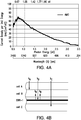
- FIG. 4A is a graph of the current density per unit energy versus the photon energy and the wavelength of the incoming light in a solar cell under the AM0 spectral environment.
- Fig. 4B is a schematic representation of photons of different wavelengths being absorbed by, or being transmitted through, different subcells in a three junction tandem solar cell with a single DBR structure (DBR-1).
- DBR-1 DBR structure
- the top subcell A is designed to absorb light of wavelength ⁇ A
- the middle subcell is designed to absorb light of wavelength ⁇ B
- the bottom subcell is designed to absorb light of wavelength ⁇ C.
- FIG. 5A is a graph 500 of the reflectance of a single distributed Bragg reflector structure as a function of wavelength such as known in the prior art.
- the wavelengths of light which are most strongly reflected extend over the range 790 to 910 nm.
- subcell B would absorb light in the wavelength range of 790 to 910 nm
- this DBR structure below subcell B will reflect any light entering the DBR structure of that wavelength back into subcell B, to allow photons of such wavelength to make a second pass through subcell B, increasing the photocurrent of subcell B.
- FIG. 5B is a graph 501 of the reflectance of a first distributed Bragg reflector (DBR-2) structure according to the present disclosure compared with that of the graph 500 of FIG. 5A .
- DBR-2 distributed Bragg reflector
- the wavelengths of light which are most strongly reflected by DBR-2 extend over the range 850 to 920 nm.
- subcell B would absorb light in the wavelength range of 790 to 910 nm
- employment of DBR-1 below subcell B will reflect any light entering DBR-1 of wavelength range 850 to 920 nm back into subcell B to allow photons of such wavelength to make a second pass through subcell B, increasing the photocurrent of subcell B.
- FIG. 5C is a graph 502 of the reflectance of a second distributed Bragg reflector (DBR-1) structure according to the present disclosure compared with that of graph 500 of FIG. 5A .
- DBR-1 distributed Bragg reflector
- the present disclosure contemplates the use of both DBR-2 and DBR-1 to more finely tune or accurately cover the wavelength range to be reflected back into subcell B compared with the single DBR structure of FIG. 5A .
- FIG. 6 is a schematic representation of photons of different wavelengths ( ⁇ A, ⁇ B1, ⁇ B2, ⁇ C) being absorbed by, or being transmitted through, different subcells in a solar cell that includes two distributed Bragg reflector (DBR) structures DBR-1 and DBR-2 according to the present disclosure.
- DBR distributed Bragg reflector
- FIG. 7A is a graph of the quantum efficiency versus wavelength in a three junction solar cell, represented by the top cell graph 601, the middle cell graph 602, and the bottom cell graph 603.
- FIG. 7B is a graph of the quantum efficiency versus wavelength in a three junction solar cell after incorporation of a structure in the solar cell according to the present disclosure.
- FIG. 8 is a graph of the doping profile in the base and emitter layers of a subcell in the solar cell according to the present disclosure.
- at least the base of at least one of the first A, second B or third C solar subcells has a graded doping, i.e., the level of doping varies from one surface to the other throughout the thickness of the base layer.
- the gradation in doping is exponential. In some embodiments, the gradation in doping is incremental and monotonic.
- the emitter of at least one of the first A, second B or third C solar subcells also has a graded doping, i.e., the level of doping varies from one surface to the other throughout the thickness of the emitter layer. In some embodiments, the gradation in doping is linear or monotonically decreasing.
- the doping profile of the emitter and base layers may be illustrated in FIG. 8 , which depicts the amount of doping in the emitter region and the base region of a subcell.
- N-type dopants include silicon, selenium, sulfur, germanium or tin.
- P-type dopants include silicon, zinc, chromium, or germanium.
- the emitter doping decreases from anywhere in the range of approximately 5 x 10¹⁸ to 1 x 10¹⁷ free carriers per cubic centimeter in the region immediately adjacent the adjoining layer to anywhere in the range of 1 x 10 18 to 1 x 10 15 free carriers per cubic centimeter in the region adjacent to the p-n junction which is shown by the dotted line in the referenced Figure.
- the base doping increases from anywhere in the range of 1 x 10 15 to 1 x 10 18 free carriers per cubic centimeter adjacent the p-n junction to anywhere in the range of 1 x 10 16 to 1 x 10 19 free carriers per cubic centimeter adjacent to the adjoining layer at the rear of the base.
- the doping level throughout the thickness of the base layer may be exponentially graded from the range of 1 x 10 16 free carriers per cubic centimeter to 1 x 10 18 free carriers per cubic centimeter, as represented by the curve 613 depicted in Figure 8 .
- the doping level throughout the thickness of the emitter layer may decline linearly from 5 x 10 18 free carriers per cubic centimeter to 5 x 10 17 free carriers per cubic centimeter as represented by the curve 612 depicted in Figure 8 .
- the exponential doping profile taught by the present disclosure produces a constant field in the doped region.
- the bottom subcell has the smallest short circuit current among all the subcells. Since in a multijunction solar cell, the individual subcells are stacked and form a series circuit, the total current flow in the entire solar cell is therefore limited by the smallest current produced in any of the subcells. Thus, by increasing the short circuit current in the bottom cell, the current more closely approximates that of the higher subcells, and the overall efficiency of the solar cell is increased as well. In addition to an increase in efficiency, the collection field created by the exponential doping profile will enhance the radiation hardness of the solar cell, which is important for spacecraft applications.
- the exponentially doped profile is the doping design which has been implemented and verified, other doping profiles may give rise to a linear varying collection field which may offer yet other advantages.
- a doping profile may be chosen to produce a linear field in the doped region which would be advantageous for both minority carrier collection and for radiation hardness at the end-of-life (EOL) of the solar cell.
- EOL end-of-life
- the composition of the window layer is linearly graded so that the concentration of Al in the window layer linearly increases from the bottom surface of the window layer to the top surface of the window layer.
- the window layer is composed of InAlP or InGaP and the Al content at the bottom surface of the window layer is between 40.0 and 48.5% by mole fraction.
- the composition of the window layer is graded so that the lattice constant in the window layer is in compression at the bottom surface of the window layer, and increases to the top surface of the window layer so that the lattice constant in the window layer is in compression at the top surface.
- the subcells may alternatively be contacted by means of metal contacts to laterally conductive semiconductor layers between the subcells. Such arrangements may be used to form 3-terminal, 4-terminal, and in general, n-terminal devices.
- the subcells can be interconnected in circuits using these additional terminals such that most of the available photogenerated current density in each subcell can be used effectively, leading to high efficiency for the multijunction cell, notwithstanding that the photogenerated current densities are typically different in the various subcells.
- the solar cell described in the present disclosure may utilize an arrangement of one or more, or all, homojunction cells or subcells, i.e., a cell or subcell in which the p-n junction is formed between a p-type semiconductor and an n-type semiconductor both of which have the same chemical composition and the same band gap, differing only in the dopant species and types, and one or more heterojunction cells or subcells.
- Subcell 309, with p-type and n-type InGaP is one example of a homojunction subcell.
- a thin so-called “intrinsic layer” may be placed between the emitter layer and base layer, with the same or different composition from either the emitter or the base layer.
- the intrinsic layer may function to suppress minority-carrier recombination in the space-charge region.
- either the base layer or the emitter layer may also be intrinsic or not-intentionally-doped ("NID”) over part or all of its thickness.
- the composition of the window or BSF layers may utilize other semiconductor compounds, subject to lattice constant and band gap requirements, and may include AlInP, AlAs, AIP, AlGaInP, AIGaAsP, AlGaInAs, AlGaInPAs, GalnP, GaInAs, GaInPAs, AIGaAs, AlInAs, AlInPAs, GaAsSb, AlAsSb, GaAIAsSb, AllnSb, GaInSb, AlGaInSb, AIN, GaN, InN, GalnN, AlGaInN, GaInNAs, AlGaInNAs, ZnSSe, CdSSe, and similar materials, and still fall within the spirit of the present invention.
- thermophotovoltaic (TPV) cells thermophotovoltaic (TPV) cells
- photodetectors and light-emitting diodes LEDS
- TPV thermophotovoltaic
- LEDs light-emitting diodes
- photodetectors can be the same materials and structures as the photovoltaic devices described above, but perhaps more lightly-doped for sensitivity rather than power production.
- LEDs can also be made with similar structures and materials, but perhaps more heavily-doped to shorten recombination time, thus radiative lifetime to produce light instead of power. Therefore, this invention also applies to photodetectors and LEDs with structures, compositions of matter, articles of manufacture, and improvements as described above for photovoltaic cells.
Landscapes
- Engineering & Computer Science (AREA)
- General Physics & Mathematics (AREA)
- Microelectronics & Electronic Packaging (AREA)
- Power Engineering (AREA)
- Computer Hardware Design (AREA)
- Electromagnetism (AREA)
- Physics & Mathematics (AREA)
- Condensed Matter Physics & Semiconductors (AREA)
- Life Sciences & Earth Sciences (AREA)
- Chemical & Material Sciences (AREA)
- Sustainable Development (AREA)
- Crystallography & Structural Chemistry (AREA)
- Sustainable Energy (AREA)
- Inorganic Chemistry (AREA)
- Photovoltaic Devices (AREA)
Priority Applications (1)
| Application Number | Priority Date | Filing Date | Title |
|---|---|---|---|
| EP20161374.2A EP3876291A1 (de) | 2020-03-06 | 2020-03-06 | Verteilte bragg-reflektorstrukturen in mehrfachübergangssolarzellen |
Applications Claiming Priority (1)
| Application Number | Priority Date | Filing Date | Title |
|---|---|---|---|
| EP20161374.2A EP3876291A1 (de) | 2020-03-06 | 2020-03-06 | Verteilte bragg-reflektorstrukturen in mehrfachübergangssolarzellen |
Publications (1)
| Publication Number | Publication Date |
|---|---|
| EP3876291A1 true EP3876291A1 (de) | 2021-09-08 |
Family
ID=69779946
Family Applications (1)
| Application Number | Title | Priority Date | Filing Date |
|---|---|---|---|
| EP20161374.2A Pending EP3876291A1 (de) | 2020-03-06 | 2020-03-06 | Verteilte bragg-reflektorstrukturen in mehrfachübergangssolarzellen |
Country Status (1)
| Country | Link |
|---|---|
| EP (1) | EP3876291A1 (de) |
Citations (7)
| Publication number | Priority date | Publication date | Assignee | Title |
|---|---|---|---|---|
| US8962993B2 (en) | 2011-11-15 | 2015-02-24 | Solar Junction Corporation | High efficiency multijunction solar cells |
| US20170200845A1 (en) * | 2016-01-12 | 2017-07-13 | The Boeing Company | Structures for Increased Current Generation and Collection in Solar Cells with Low Absorptance and/or Low Diffusion Length |
| EP3370265A1 (de) * | 2017-03-03 | 2018-09-05 | SolAero Technologies Corp. | Verteilte bragg-reflektorstrukturen in mehrfachübergangssolarzellen |
| EP3514838A1 (de) * | 2018-01-17 | 2019-07-24 | SolAero Technologies Corp. | Solarzelle mit vierfachabzweigung und solarzellenanordnungen für raumfahrtanwendungen |
| CN110491957A (zh) * | 2019-07-25 | 2019-11-22 | 中山德华芯片技术有限公司 | 应用于晶格失配太阳能电池外延生长的晶格渐变缓冲层 |
| WO2019237155A1 (en) * | 2018-06-13 | 2019-12-19 | Newsouth Innovations Pty Limited | A photovoltaic cell structure |
| US10559705B1 (en) * | 2016-05-11 | 2020-02-11 | Solaero Technologies Corp. | Multijunction solar cells having a graded-index reflector structure |
-
2020
- 2020-03-06 EP EP20161374.2A patent/EP3876291A1/de active Pending
Patent Citations (7)
| Publication number | Priority date | Publication date | Assignee | Title |
|---|---|---|---|---|
| US8962993B2 (en) | 2011-11-15 | 2015-02-24 | Solar Junction Corporation | High efficiency multijunction solar cells |
| US20170200845A1 (en) * | 2016-01-12 | 2017-07-13 | The Boeing Company | Structures for Increased Current Generation and Collection in Solar Cells with Low Absorptance and/or Low Diffusion Length |
| US10559705B1 (en) * | 2016-05-11 | 2020-02-11 | Solaero Technologies Corp. | Multijunction solar cells having a graded-index reflector structure |
| EP3370265A1 (de) * | 2017-03-03 | 2018-09-05 | SolAero Technologies Corp. | Verteilte bragg-reflektorstrukturen in mehrfachübergangssolarzellen |
| EP3514838A1 (de) * | 2018-01-17 | 2019-07-24 | SolAero Technologies Corp. | Solarzelle mit vierfachabzweigung und solarzellenanordnungen für raumfahrtanwendungen |
| WO2019237155A1 (en) * | 2018-06-13 | 2019-12-19 | Newsouth Innovations Pty Limited | A photovoltaic cell structure |
| CN110491957A (zh) * | 2019-07-25 | 2019-11-22 | 中山德华芯片技术有限公司 | 应用于晶格失配太阳能电池外延生长的晶格渐变缓冲层 |
Non-Patent Citations (2)
| Title |
|---|
| CHAO-GANG LOU ET AL.: "Current-Enhanced Quantum Well Solar Cells", CHINESE PHYSICS LETTERS, vol. 23, no. 1, 2006, XP020096547, DOI: 10.1088/0256-307X/23/1/071 |
| M. MAZZER ET AL.: "Progress in Quantum Well Solar Cells", THIN SOLID FILMS, vol. 511-512, 26 July 2006 (2006-07-26), XP025007150, DOI: 10.1016/j.tsf.2005.12.120 |
Similar Documents
| Publication | Publication Date | Title |
|---|---|---|
| US20200251603A1 (en) | Distributed bragg reflector structures in multijunction solar cells | |
| US11670728B2 (en) | Multijunction metamorphic solar cells | |
| US10714636B2 (en) | Method for forming a multijunction metamorphic solar cell for space applications | |
| US20170054048A1 (en) | Four junction solar cell for space applications | |
| US10749053B2 (en) | Distributed Bragg reflector structures in multijunction solar cells | |
| US20170062642A1 (en) | Inverted metamorphic multijunction solar cell | |
| US11387377B2 (en) | Multijunction solar cell assembly for space applications | |
| US11721777B1 (en) | Multijunction metamorphic solar cell | |
| US11282979B2 (en) | Distributed bragg reflector structures in multijunction solar cells | |
| US20210242360A1 (en) | Multijunction metamorphic solar cell | |
| US11316053B2 (en) | Multijunction solar cell assembly | |
| US10256359B2 (en) | Lattice matched multijunction solar cell assemblies for space applications | |
| US11784272B2 (en) | Multijunction solar cell | |
| EP3876291A1 (de) | Verteilte bragg-reflektorstrukturen in mehrfachübergangssolarzellen | |
| US11784273B2 (en) | Multijunction metamorphic solar cell | |
| US20230178679A1 (en) | Method of fabricating metamorphic multijunction solar cells for space applications | |
| US11264524B1 (en) | Multijunction solar cells | |
| US20220393055A1 (en) | Multijunction metamorphic solar cells | |
| US11563133B1 (en) | Method of fabricating multijunction solar cells for space applications |
Legal Events
| Date | Code | Title | Description |
|---|---|---|---|
| PUAI | Public reference made under article 153(3) epc to a published international application that has entered the european phase |
Free format text: ORIGINAL CODE: 0009012 |
|
| STAA | Information on the status of an ep patent application or granted ep patent |
Free format text: STATUS: THE APPLICATION HAS BEEN PUBLISHED |
|
| AK | Designated contracting states |
Kind code of ref document: A1 Designated state(s): AL AT BE BG CH CY CZ DE DK EE ES FI FR GB GR HR HU IE IS IT LI LT LU LV MC MK MT NL NO PL PT RO RS SE SI SK SM TR |
|
| STAA | Information on the status of an ep patent application or granted ep patent |
Free format text: STATUS: REQUEST FOR EXAMINATION WAS MADE |
|
| RIN1 | Information on inventor provided before grant (corrected) |
Inventor name: MCGLYNN, DANIEL Inventor name: DERKACS, DANIEL |
|
| 17P | Request for examination filed |
Effective date: 20220224 |
|
| RBV | Designated contracting states (corrected) |
Designated state(s): AL AT BE BG CH CY CZ DE DK EE ES FI FR GB GR HR HU IE IS IT LI LT LU LV MC MK MT NL NO PL PT RO RS SE SI SK SM TR |