EP3133650B1 - Solarzelle mit vierfachabzweigung für raumfahrtanwendungen - Google Patents
Solarzelle mit vierfachabzweigung für raumfahrtanwendungen Download PDFInfo
- Publication number
- EP3133650B1 EP3133650B1 EP16182474.3A EP16182474A EP3133650B1 EP 3133650 B1 EP3133650 B1 EP 3133650B1 EP 16182474 A EP16182474 A EP 16182474A EP 3133650 B1 EP3133650 B1 EP 3133650B1
- Authority
- EP
- European Patent Office
- Prior art keywords
- subcell
- band gap
- layer
- solar cell
- solar
- Prior art date
- Legal status (The legal status is an assumption and is not a legal conclusion. Google has not performed a legal analysis and makes no representation as to the accuracy of the status listed.)
- Active
Links
Images


Classifications
-
- H—ELECTRICITY
- H10—SEMICONDUCTOR DEVICES; ELECTRIC SOLID-STATE DEVICES NOT OTHERWISE PROVIDED FOR
- H10F—INORGANIC SEMICONDUCTOR DEVICES SENSITIVE TO INFRARED RADIATION, LIGHT, ELECTROMAGNETIC RADIATION OF SHORTER WAVELENGTH OR CORPUSCULAR RADIATION
- H10F10/00—Individual photovoltaic cells, e.g. solar cells
- H10F10/10—Individual photovoltaic cells, e.g. solar cells having potential barriers
- H10F10/16—Photovoltaic cells having only PN heterojunction potential barriers
- H10F10/161—Photovoltaic cells having only PN heterojunction potential barriers comprising multiple PN heterojunctions, e.g. tandem cells
-
- H—ELECTRICITY
- H10—SEMICONDUCTOR DEVICES; ELECTRIC SOLID-STATE DEVICES NOT OTHERWISE PROVIDED FOR
- H10F—INORGANIC SEMICONDUCTOR DEVICES SENSITIVE TO INFRARED RADIATION, LIGHT, ELECTROMAGNETIC RADIATION OF SHORTER WAVELENGTH OR CORPUSCULAR RADIATION
- H10F10/00—Individual photovoltaic cells, e.g. solar cells
- H10F10/10—Individual photovoltaic cells, e.g. solar cells having potential barriers
- H10F10/16—Photovoltaic cells having only PN heterojunction potential barriers
- H10F10/163—Photovoltaic cells having only PN heterojunction potential barriers comprising only Group III-V materials, e.g. GaAs/AlGaAs or InP/GaInAs photovoltaic cells
-
- H—ELECTRICITY
- H10—SEMICONDUCTOR DEVICES; ELECTRIC SOLID-STATE DEVICES NOT OTHERWISE PROVIDED FOR
- H10F—INORGANIC SEMICONDUCTOR DEVICES SENSITIVE TO INFRARED RADIATION, LIGHT, ELECTROMAGNETIC RADIATION OF SHORTER WAVELENGTH OR CORPUSCULAR RADIATION
- H10F10/00—Individual photovoltaic cells, e.g. solar cells
- H10F10/10—Individual photovoltaic cells, e.g. solar cells having potential barriers
- H10F10/19—Photovoltaic cells having multiple potential barriers of different types, e.g. tandem cells having both PN and PIN junctions
-
- H—ELECTRICITY
- H10—SEMICONDUCTOR DEVICES; ELECTRIC SOLID-STATE DEVICES NOT OTHERWISE PROVIDED FOR
- H10F—INORGANIC SEMICONDUCTOR DEVICES SENSITIVE TO INFRARED RADIATION, LIGHT, ELECTROMAGNETIC RADIATION OF SHORTER WAVELENGTH OR CORPUSCULAR RADIATION
- H10F71/00—Manufacture or treatment of devices covered by this subclass
- H10F71/127—The active layers comprising only Group III-V materials, e.g. GaAs or InP
- H10F71/1272—The active layers comprising only Group III-V materials, e.g. GaAs or InP comprising at least three elements, e.g. GaAlAs or InGaAsP
-
- H—ELECTRICITY
- H10—SEMICONDUCTOR DEVICES; ELECTRIC SOLID-STATE DEVICES NOT OTHERWISE PROVIDED FOR
- H10F—INORGANIC SEMICONDUCTOR DEVICES SENSITIVE TO INFRARED RADIATION, LIGHT, ELECTROMAGNETIC RADIATION OF SHORTER WAVELENGTH OR CORPUSCULAR RADIATION
- H10F71/00—Manufacture or treatment of devices covered by this subclass
- H10F71/127—The active layers comprising only Group III-V materials, e.g. GaAs or InP
- H10F71/1276—The active layers comprising only Group III-V materials, e.g. GaAs or InP comprising growth substrates not made of Group III-V materials
-
- H—ELECTRICITY
- H10—SEMICONDUCTOR DEVICES; ELECTRIC SOLID-STATE DEVICES NOT OTHERWISE PROVIDED FOR
- H10F—INORGANIC SEMICONDUCTOR DEVICES SENSITIVE TO INFRARED RADIATION, LIGHT, ELECTROMAGNETIC RADIATION OF SHORTER WAVELENGTH OR CORPUSCULAR RADIATION
- H10F77/00—Constructional details of devices covered by this subclass
- H10F77/40—Optical elements or arrangements
- H10F77/413—Optical elements or arrangements directly associated or integrated with the devices, e.g. back reflectors
-
- H—ELECTRICITY
- H10—SEMICONDUCTOR DEVICES; ELECTRIC SOLID-STATE DEVICES NOT OTHERWISE PROVIDED FOR
- H10F—INORGANIC SEMICONDUCTOR DEVICES SENSITIVE TO INFRARED RADIATION, LIGHT, ELECTROMAGNETIC RADIATION OF SHORTER WAVELENGTH OR CORPUSCULAR RADIATION
- H10F77/00—Constructional details of devices covered by this subclass
- H10F77/80—Arrangements for preventing damage to photovoltaic cells caused by corpuscular radiation, e.g. for space applications
-
- Y—GENERAL TAGGING OF NEW TECHNOLOGICAL DEVELOPMENTS; GENERAL TAGGING OF CROSS-SECTIONAL TECHNOLOGIES SPANNING OVER SEVERAL SECTIONS OF THE IPC; TECHNICAL SUBJECTS COVERED BY FORMER USPC CROSS-REFERENCE ART COLLECTIONS [XRACs] AND DIGESTS
- Y02—TECHNOLOGIES OR APPLICATIONS FOR MITIGATION OR ADAPTATION AGAINST CLIMATE CHANGE
- Y02E—REDUCTION OF GREENHOUSE GAS [GHG] EMISSIONS, RELATED TO ENERGY GENERATION, TRANSMISSION OR DISTRIBUTION
- Y02E10/00—Energy generation through renewable energy sources
- Y02E10/50—Photovoltaic [PV] energy
- Y02E10/544—Solar cells from Group III-V materials
-
- Y—GENERAL TAGGING OF NEW TECHNOLOGICAL DEVELOPMENTS; GENERAL TAGGING OF CROSS-SECTIONAL TECHNOLOGIES SPANNING OVER SEVERAL SECTIONS OF THE IPC; TECHNICAL SUBJECTS COVERED BY FORMER USPC CROSS-REFERENCE ART COLLECTIONS [XRACs] AND DIGESTS
- Y02—TECHNOLOGIES OR APPLICATIONS FOR MITIGATION OR ADAPTATION AGAINST CLIMATE CHANGE
- Y02P—CLIMATE CHANGE MITIGATION TECHNOLOGIES IN THE PRODUCTION OR PROCESSING OF GOODS
- Y02P70/00—Climate change mitigation technologies in the production process for final industrial or consumer products
- Y02P70/50—Manufacturing or production processes characterised by the final manufactured product
Definitions
- the present disclosure relates to solar cells and the fabrication of solar cells, and more particularly the design and specification of the band gaps in a four junction solar cell based on III-V semiconductor compounds.
- III-V compound semiconductor multijunction solar cells Solar power from photovoltaic cells, also called solar cells, has been predominantly provided by silicon semiconductor technology.
- high-volume manufacturing of III-V compound semiconductor multijunction solar cells for space applications has accelerated the development of such technology not only for use in space but also for terrestrial solar power applications.
- III-V compound semiconductor multijunction devices have greater energy conversion efficiencies and generally more radiation resistance, although they tend to be more complex to manufacture.
- Typical commercial III-V compound semiconductor multijunction solar cells have energy efficiencies that exceed 27% under one sun, air mass 0 (AM0), illumination, whereas even the most efficient silicon technologies generally reach only about 18% efficiency under comparable conditions.
- III-V compound semiconductor multijunction solar cells Under high solar concentration (e.g., 500X), commercially available III-V compound semiconductor multijunction solar cells in terrestrial applications (at AM1.5D) have energy efficiencies that exceed 37%.
- the higher conversion efficiency of III-V compound semiconductor solar cells compared to silicon solar cells is in part based on the ability to achieve spectral splitting of the incident radiation through the use of a plurality of photovoltaic regions with different band gap energies, and accumulating the current from each of the regions.
- Typical III-V compound semiconductor solar cells are fabricated on a semiconductor wafer in vertical, multifunction structures or stacked sequence of solar subcells, each subcell formed with appropriate semiconductor layers and including a p-n photoactive junction. Each subcell is designed to convert photons over different spectral or wavelength bands to electrical current. After the sunlight impinges on the front of the solar cell, and photons pass through the subcells, the photons in a wavelength band that are not absorbed and converted to electrical energy in the region of one subcell propagate to the next subcell, where such photons are intended to be captured and converted to electrical energy, assuming the downstream subcell is designed for the photon's particular wavelength or energy band.
- the energy conversion efficiency of multijunction solar cells is affected by such factors as the number of subcells, the thickness of each subcell, the composition and doping of each active layer in a subcell, and the consequential band structure, electron energy levels, conduction, and absorption of each subcell.
- Factors such as the short circuit current density (J sc ), the open circuit voltage (V oc ), and the fill factor are also important.
- Another parameter of consideration is the difference between the band gap and the open circuit voltage, or (E g - V oc ), of a particular active layer.
- One of the important mechanical or structural considerations in the choice of semiconductor layers for a solar cell is the desirability of the adjacent layers of semiconductor materials in the solar cell, i.e. each layer of crystalline semiconductor material that is deposited and grown to form a solar subcell, have similar crystal lattice constants or parameters.
- the present application is directed to solar cells with substantially lattice matched subcells.
- PROCEEDINGS OF THE 29TH EUROPEAN PHOTOVOLTAIC SOLAR ENERGY CONFERENCE AND EXHIBITION, 3 November 2014 (2014-11-03), XP040677850, ISBN 978-3-936338-34-8 discloses a four junction lattice matched solar cell. However, the average band gap value of the four subcells is 1.43 eV.
- a predetermined high temperature in the range of 50 to 70 degrees Centigrade
- the present disclosure provides a solar cell and a method of manufacturing the same, the solar cell comprising an upper first solar subcell composed of a semiconductor material having a first band gap; a second solar subcell adjacent to said first solar subcell composed of a semiconductor material having a second band gap smaller than the first band gap and being lattice matched with the upper first solar subcell; a third solar subcell adjacent to said second solar subcell and composed of a semiconductor material having a third band gap smaller than the second band gap and being lattice matched with the second solar subcell; and a fourth solar subcell adjacent to said third solar subcell and composed of a semiconductor material having a fourth band gap smaller than the third band gap; wherein the fourth subcell has a bandgap of approximately 0.67 eV, the third subcell has a band gap of approximately 1.41 eV, the second subcell has a band gap in the range of 1.65 to 1.8 eV and the upper first subcell has a band gap in the range of 2.0 to 2.15
- the upper first subcell is composed of indium gallium aluminum phosphide;
- the second solar subcell includes an emitter layer composed of indium gallium phosphide or aluminum gallium arsenide, and a base layer composed of aluminum gallium arsenide;
- the third solar subcell is composed of indium gallium arsenide; and
- the fourth subcell is composed of germanium
- DBR distributed Bragg reflector
- the present disclosure is directed to the fabrication of a multijunction lattice matched solar cell grown on a single growth substrate. More specifically, however, the present disclosure relates to four junction solar cells with direct band gaps in the range of 2.0 to 2.15 eV for the top subcell, and (i) 1.65 to 1.8 eV, and (ii) 1.41 eV for the middle subcells, and 0.67 eV indirect bandgaps, for the bottom subcell, respectively.
- the present disclosure intends to provide a relatively simple and reproducible technique that does not employ inverted processing associated with inverted metamorphic multijunction solar cells, and is suitable for use in a high volume production environment in which various semiconductor layers are grown on a growth substrate in an MOCVD reactor, and subsequent processing steps are defined and selected to minimize any physical damage to the quality of the deposited layers, thereby ensuring a relatively high yield of operable solar cells meeting specifications at the conclusion of the fabrication processes.
- One aspect of the present disclosure relates to the use of aluminum in the active layers of the upper subcells in a multijunction solar cell
- the effects of increasing amounts of aluminum as a constituent element in an active layer of a subcell affects the photovoltaic device performance.
- One measure of the "quality" or “goodness” of a solar cell junction is the difference between the band gap of the semiconductor material in that subcell or junction and the V oc , or open circuit voltage, of that same junction. The smaller the difference, the higher the V oc of the solar cell junction relative to the band gap, and the better the performance of the device.
- V oc is very sensitive to semiconductor material quality, so the smaller the E g - V oc of a device, the higher the quality of the material in that device.
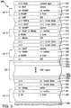
- FIG. 2 illustrates a particular example of a multijunction solar cell device 303 as known in the prior art.
- each dashed line indicates the active region junction between a base layer and emitter layer of a subcell.
- the bottom subcell 205 includes a substrate 212 formed of p-type germanium ("Ge") which also serves as a base layer.
- a contact pad 213 formed on the bottom of base layer 212 provides electrical contact to the multifunction solar cell 203.
- the bottom subcell 205 further includes, for example, a highly doped n-type Ge emitter layer 214, and an n-type indium gallium arsenide (“InGaAs”) nucleation layer 216.
- the nucleation layer is deposited over the base layer 212, and the emitter layer is formed in the substrate by diffusion of deposits into the Ge substrate, thereby forming the n-type Ge layer 214.
- Heavily doped p-type aluminum gallium arsenide (“AlGaAs”) and heavily doped n-type gallium arsenide (“GaAs”) tunneling junction layers 218, 217 may be deposited over the nucleation layer 216 to provide a low resistance pathway between the bottom and middle subcells. In the illustrated example of FIG.
- the middle subcell 207 includes a highly doped p-type aluminum gallium arsenide ("AlGaAs”) back surface field (“BSF") layer 220, a p-type InGaAs base layer 222, a highly doped n-type indium gallium phosphide (“InGaP2”) emitter layer 224 and a highly doped n-type indium aluminum phosphide (“AlInP2”) window layer 226.
- the InGaAs base layer 222 of the middle subcell 207 can include, for example, approximately 1.5% In. Other compositions may be used as well.
- the base layer 222 is formed over the BSF layer 220 after the BSF layer is deposited over the tunneling junction layers 218 of the bottom subcell 204.
- the BSF layer 220 is provided to reduce the recombination loss in the middle subcell 207.
- the BSF layer 220 drives minority carriers from a highly doped region near the back surface to minimize the effect of recombination loss.
- the BSF layer 220 reduces recombination loss at the backside of the solar cell and thereby reduces recombination at the base layer/BSF layer interface.
- the window layer 226 is deposited on the emitter layer 224 of the middle subcell B.
- the window layer 226 in the middle subcell B also helps reduce the recombination loss and improves passivation of the cell surface of the underlying junctions.
- heavily doped n-type InGaP and p-type AlGaAs tunneling junction layers 227, 228 may be deposited over the middle subcell B.
- the top subcell 209 includes a highly doped p-type indium gallium aluminum phosphide ("InGaAlP") BSF layer 230, a p-type InGaP2 base layer 232, a highly doped n-type InGaP2 emitter layer 234 and a highly doped n-type InAlP2 window layer 236.
- InGaAlP indium gallium aluminum phosphide
- the base layer 232 of the top subcell 209 is deposited over the BSF layer 230 after the BSF layer 230 is formed over the tunneling junction layers 228 of the middle subcell 207.
- the window layer 236 is deposited over the emitter layer 234 of the top subcell after the emitter layer 234 is formed over the base layer 232.
- a cap or contact layer 238 may be deposited and patterned into separate contact regions over the window layer 236 of the top subcell 208.
- the cap or contact layer 238 serves as an electrical contact from the top subcell 209 to metal grid layer 240.
- the doped cap or contact layer 238 can be a semiconductor layer such as, for example, a GaAs or InGaAs layer.
- the grid lines 240 are formed.
- the grid lines 240 are deposited via evaporation and lithographically patterned and deposited over the cap or contact layer 238.
- the mask is subsequently lifted off to form the finished metal grid lines 240 as depicted in the Figure, and the portion of the cap layer that has not been metallized is removed, exposing the surface 242 of the window layer 236.
- a trench or channel (not shown), or portion of the semiconductor structure, is also etched around each of the solar cells.
- These channels define a peripheral boundary between the solar cell (later to be scribed from the wafer) and the rest of the wafer, and leaves a mesa structure (or a plurality of mesas, in the case of more than one solar cell per wafer) which define and constitute the solar cells later to be scribed and diced from the wafer.
- the grid lines 240 are composed of Ti/Au/Ag/Au, although other suitable materials may be used as well.
- the bottom subcell D includes a substrate 300 formed of p-type germanium ("Ge") which also serves as a base layer.
- a back metal contact pad 350 formed on the bottom of base layer 300 provides electrical contact to the multijunction solar cell 400.
- the bottom subcell D further includes, for example, a highly doped n-type Ge emitter layer 301, and an n-type indium gallium arsenide (“InGaAs”) nucleation layer 302.
- the nucleation layer is deposited over the base layer, and the emitter layer is formed in the substrate by diffusion of deposits into the Ge substrate, thereby forming the n-type Ge layer 301.
- Heavily doped p-type aluminum gallium arsenide (“AlGaAs”) and heavily doped n-type gallium arsenide (“GaAs”) tunneling junction layers 303, 304 may be deposited over the nucleation layer to provide a low resistance pathway between the bottom and middle subcells.
- Distributed Bragg reflector (DBR) layers 305 are then grown adjacent to and between the tunnel diode 303, 304 of the bottom subcell D and the third solar subcell C.
- DBR Distributed Bragg reflector
- the DBR layers 305 are arranged so that light can enter and pass through the third solar subcell C and at least a portion of which can be reflected back into the third solar subcell C by the DBR layers 305.
- the distributed Bragg reflector (DBR) layers 305 are specifically located between the third solar subcell C and tunnel diode layers 304, 303; in other embodiments, the distributed Bragg reflector (DBR) layers may be located between tunnel diode layers 304/303 and buffer layer 302.
- distributed Bragg reflector (DBR) layers 305 can be composed of a plurality of alternating layers 305a through 305z of lattice matched materials with discontinuities in their respective indices of refraction.
- distributed Bragg reflector (DBR) layers 305a through 305z includes a first DBR layer composed of a plurality of p type Al x Ga 1-x As layers, and a second DBR layer disposed over the first DBR layer and composed of a plurality of p type Al y Ga 1-y As layers, where y is greater than x.
- DBR distributed Bragg reflector
- the subcell C includes a highly doped p-type aluminum gallium arsenide ("AlGaAs”) back surface field (“BSF") layer 306, a p-type InGaAs base layer 307, a highly doped n-type indium gallium arsenide (“InGaAs”) emitter layer 308 and a highly doped n-type indium aluminum phosphide (“AlInP2”) window layer 309.
- the InGaAs base layer 307 of the subcell C can include, for example, approximately 1.5% In. Other compositions may be used as well.
- the base layer 307 is formed over the BSF layer 306 after the BSF layer is deposited over the DBR layers 305.
- the window layer 309 is deposited on the emitter layer 308 of the subcell C.
- the window layer 309 in the subcell C also helps reduce the recombination loss and improves passivation of the cell surface of the underlying junctions.
- tunneling junction layers 310, 311 may be deposited over the subcell C.
- the middle subcell B includes a highly doped p-type aluminum gallium arsenide ("AlGaAs”) back surface field (“BSF") layer 312, a p-type AlGaAs base layer 313, a highly doped n-type indium gallium phosphide ("InGaP2”) or AlGaAs layer 314 and a highly doped n-type indium gallium aluminum phosphide (“AlGaAlP”) window layer 315.
- the InGaP emitter layer 314 of the subcell B can include, for example, approximately 50% In. Other compositions may be used as well.
- the top subcell A includes a highly doped p-type indium aluminum phosphide ("InAlP2") BSF layer 318, a p-type InGaAlP base layer 319, a highly doped n-type InGaAlP emitter layer 320 and a highly doped n-type InAlP2 window layer 321.
- the base layer 319 of the top subcell A is deposited over the BSF layer 318 after the BSF layer 318 is formed.
- the grid lines are formed via evaporation and lithographically patterned and deposited over the cap or contact layer 322.
- the present disclosure provides a multijunction solar cell that follows a design rule that one should incorporate as many high band gap subcells as possible to achieve the goal to increase the efficiency at high temperature EOL.
- high band gap subcells may retain a greater percentage of cell voltage as temperature increases, thereby offering lower power loss as temperature increases.
- both HT-BOL and HT-EOL performance of the exemplary multijunction solar cell, according to the present disclosure may be expected to be greater than traditional cells.
- the cell efficiency (%) measured at room temperature (RT) 28° C and high temperature (HT) 70° C, at beginning of life (BOL) and end of life (EOL), for a standard three junction commercial solar cell (ZTJ), such as depicted in FIG. 2 is as follows: Condition Efficiency BOL 28° C 29.1% BOL 70° C 26.4% EOL 70° C 23.4% After 5E14 e/cm 2 radiation EOL 70°C 22.0% After 1E15 e/cm 2 radiation
- the new solar cell has a slightly higher cell efficiency than the standard commercial solar cell (ZTJ) at BOL at 70° C.
- the solar cell described in the present disclosure exhibits substantially improved cell efficiency (%) over the standard commercial solar cell (ZTJ) at 1 MeV electron equivalent fluence of 5 x 10 14 e/cm 2 , and dramatically improved cell efficiency (%) over the standard commercial solar cell (ZTJ) at 1 MeV electron equivalent fluence of 1 x 10 15 e/cm 2 .
- a low earth orbit (LEO) satellite will typically experience radiation equivalent to 5 x 10 14 e/cm 2 over a five year lifetime.
- a geosynchronous earth orbit (GEO) satellite will typically experience radiation in the range of 5 x 10 14 e/cm 2 to 1 x 10 15 e/cm 2 over a fifteen year lifetime.
- the omnidirectional space radiation is converted to a damage equivalent unidirectional fluence at a normalised energy and in terms of a specific radiation particle.
- This equivalent fluence will produce the same damage as that produced by omnidirectional space radiation considered when the relative damage coefficient (RDC) is properly defined to allow the conversion.
- the relative damage coefficients (RDCs) of a particular solar cell structure are measured a priori under many energy and fluence levels in addition to different coverglass thickness values.
- the equivalent fluence is determined for a given space environment, the parameter degradation can be evaluated in the laboratory by irradiating the solar cell with the calculated fluence level of unidirectional normally incident flux.
- the equivalent fluence is normally expressed in terms of 1 MeV electrons or 10 MeV protons.
- the software package Spenvis (www.spenvis.oma.be) is used to calculate the specific electron and proton fluence that a solar cell is exposed to during a specific satellite mission as defined by the duration, altitude, azimuth, etc.
- Spenvis employs the EQFLUX program, developed by the Jet Propulsion Laboratory (JPL) to calculate 1 MeV and 10 MeV damage equivalent electron and proton fluences, respectively, for exposure to the fluences predicted by the trapped radiation and solar proton models for a specified mission environment duration.
- JPL Jet Propulsion Laboratory
- the conversion to damage equivalent fluences is based on the relative damage coefficients determined for multifunction cells [ Marvin, D.C., Assessment of Multijunction Solar Cell Performance in Radiation Environments, Aerospace Report No. TOR-2000 (1210)-1, 2000 ].
- a widely accepted total mission equivalent fluence for a geosynchronous satellite mission of 15 year duration is 1MeV 1x10 15 electrons/cm 2 .
- the exemplary solar cell described herein requires the use of aluminum in the semiconductor composition of each of the top two subcells.
- Aluminum incorporation is widely known in the III-V compound semiconductor industry to degrade BOL subcell performance due to deep level donor defects, higher doping compensation, shorter minority carrier lifetimes, and lower cell voltage and an increased BOL E g - V oc metric.
- increased BOL E g - V oc may be the most problematic shortcoming of aluminum containing subcells; the other limitations can be mitigated by modifying the doping schedule or thinning base thicknesses.
Landscapes
- Photovoltaic Devices (AREA)
- Engineering & Computer Science (AREA)
- Life Sciences & Earth Sciences (AREA)
- Sustainable Energy (AREA)
- Manufacturing & Machinery (AREA)
- Sustainable Development (AREA)
Claims (8)
- Vierfachsolarzelle, die Folgendes umfasst:eine obere erste Solarteilzelle, die aus Indium-Gallium-Aluminium-Phosphid besteht und eine erste Bandlücke aufweist;eine der ersten Solarteilzelle benachbarte zweite Teilzelle, umfassend eine aus Indium-Gallium-Phosphid oder Aluminium-Gallium-Arsenid bestehende Emitterschicht und eine aus Aluminium-Gallium-Arsenid bestehende Basisschicht, die zweite Bandlücke aufweist, die kleiner ist als die erste Bandlücke, und die an die obere erste Solarteilzelle gitterangepasst ist;eine der zweiten Solarteilzelle benachbarte dritte Solarteilzelle, die aus Indium-Gallium-Arsenid besteht und eine dritte Bandlücke aufweist, die kleiner ist als die zweite Bandlücke, und die an die zweite Solarteilzelle gitterangepasst ist; undeine der dritten Solarteilzelle benachbarte vierte Solarteilzelle, die aus Germanium besteht und eine vierte Bandlücke aufweist, die kleiner ist als die dritte Bandlücke, wobei die vierte Teilzelle eine Bandlücke von ungefähr 0,67 eV aufweist und die zweite Teilzelle eine Bandlücke im Bereich von 1,65 bis 1,8 eV aufweist, dadurch gekennzeichnet, dass die obere erste Teilzelle eine Bandlücke im Bereich von 2,0 bis 2,15 eV aufweist und die dritte Teilzelle eine Bandlücke von ungefähr 1,41 eV aufweist, wobei die durchschnittliche Bandlücke aller vier Teilzellen, das heißt die Summe der vier Bandlücken jeder Teilzelle geteilt durch vier, größer ist als 1.44 eV.
- Vierfachsolarzelle nach Anspruch 1, wobei die zweite Teilzelle eine Bandlücke von ungefähr 1,73 eV aufweist und die obere erste Teilzelle eine Bandlücke von ungefähr 2,10 eV aufweist.
- Vierfachsolarzelle nach Anspruch 1, die ferner Folgendes umfasst:
eine Bragg-Spiegelschicht (Distributed Bragg Reflector, DBR) zwischen der dritten und der vierten Solarteilzelle und diesen benachbart, die derart angeordnet ist, dass Licht in die dritte Solarteilzelle eintreten und dadurch hindurch gelangen kann und mindestens ein Anteil davon von der DBR-Schicht in die dritte Solarteilzelle zurückreflektiert werden kann. - Vierfachsolarzelle nach Anspruch 3, wobei die Bragg-Spiegelschicht aus einer Vielzahl von abwechselnden Schichten gitterangepasster Materialien mit Diskontinuitäten in ihren entsprechenden Brechungsindizes besteht.
- Vierfachsolarzelle nach Anspruch 4, wobei die Differenz zwischen den Brechungsindizes abwechselnder Schichten maximiert ist, um die Zahl der Perioden zu minimieren, die benötigt wird, um einen gegebenen Reflexionsgrad zu erreichen, und wobei die Dicke und der Brechungsindex jeder Periode das Sperrband und dessen Grenzwellenlänge bestimmen.
- Vierfachsolarzelle nach Anspruch 5, wobei die DBR-Schicht eine aus einer Vielzahl von p-leitenden AlxGa1-xAs-Schichten bestehende erste DBR-Schicht und eine zweite DBR-Schicht, die über der ersten DBR-Schicht angeordnet ist und aus einer Vielzahl von p-leitenden AlyGa1-yAs-Schichten besteht, umfasst, wobei y größer ist als x.
- Verfahren zum Herstellen einer Vierfachsolarzelle, das Folgendes umfasst:Bereitstellen eines Germaniumsubstrats;Züchten einer Folge von Schichten aus Halbleitermaterial auf dem Germaniumsubstrat unter Verwendung eines metallorganisch-chemischen Verfahrens zur Abscheidung aus der Gasphase, um eine Solarzelle zu bilden, die eine Vielzahl von Teilzellen umfasst, die Folgendes umfasst:
eine dritte Teilzelle, die über dem Germaniumsubstrat angeordnet ist und eine Bandlücke von ungefähr 1,41 eV aufweist, eine zweite Teilzelle, die über der dritten Teilzelle angeordnet ist und eine Bandlücke im Bereich von ungefähr 1,65 bis 1,8 eV aufweist und eine obere erste Teilzelle, die über der zweiten Teilzelle angeordnet ist und eine Bandlücke im Bereich von 2,0 bis 2,15 eV aufweist, wobei die durchschnittliche Bandlücke aller vier Teilzellen, das heißt die Summe der vier Bandlücken jeder Teilzelle geteilt durch vier, größer ist als 1,44 eV. - Verfahren nach Anspruch 7, ferner umfassend das Bilden (i) einer der Unterseite der dritten Teilzelle direkt benachbarte Rückseitenfeldschicht (Back Surface Field, BSF), und (ii) mindestens einer Bragg-Spiegelschicht (Distributed Bragg Reflector, DBR) direkt unter der BSF-Schicht, sodass Licht in die erste, die zweite und die dritte Teilzelle eintreten und dadurch hindurch gelangen und mindestens ein Anteil davon von der DBR-Schicht in die dritte Teilzelle zurückreflektiert werden kann.
Applications Claiming Priority (1)
| Application Number | Priority Date | Filing Date | Title |
|---|---|---|---|
| US14/828,206 US20170054048A1 (en) | 2015-08-17 | 2015-08-17 | Four junction solar cell for space applications |
Publications (2)
| Publication Number | Publication Date |
|---|---|
| EP3133650A1 EP3133650A1 (de) | 2017-02-22 |
| EP3133650B1 true EP3133650B1 (de) | 2020-09-23 |
Family
ID=56567494
Family Applications (1)
| Application Number | Title | Priority Date | Filing Date |
|---|---|---|---|
| EP16182474.3A Active EP3133650B1 (de) | 2015-08-17 | 2016-08-02 | Solarzelle mit vierfachabzweigung für raumfahrtanwendungen |
Country Status (2)
| Country | Link |
|---|---|
| US (1) | US20170054048A1 (de) |
| EP (1) | EP3133650B1 (de) |
Cited By (1)
| Publication number | Priority date | Publication date | Assignee | Title |
|---|---|---|---|---|
| EP4036992A1 (de) | 2018-01-17 | 2022-08-03 | SolAero Technologies Corp. | Solarzelle mit vierfachabzweigung und solarzellenanordnungen für raumfahrtanwendungen |
Families Citing this family (17)
| Publication number | Priority date | Publication date | Assignee | Title |
|---|---|---|---|---|
| US10541345B2 (en) * | 2016-01-12 | 2020-01-21 | The Boeing Company | Structures for increased current generation and collection in solar cells with low absorptance and/or low diffusion length |
| US9954128B2 (en) | 2016-01-12 | 2018-04-24 | The Boeing Company | Structures for increased current generation and collection in solar cells with low absorptance and/or low diffusion length |
| US10749053B2 (en) | 2017-03-03 | 2020-08-18 | Solaero Technologies Corp. | Distributed Bragg reflector structures in multijunction solar cells |
| US11282979B2 (en) * | 2017-03-03 | 2022-03-22 | Solaero Technologies Corp. | Distributed bragg reflector structures in multijunction solar cells |
| DE102018203509B4 (de) | 2018-01-17 | 2024-10-10 | Solaero Technologies Corp. | Vierfach-Solarzelle für Raumanwendungen |
| DE102018001592A1 (de) * | 2018-03-01 | 2019-09-05 | Azur Space Solar Power Gmbh | Mehrfachsolarzelle |
| WO2019175651A1 (en) * | 2018-03-16 | 2019-09-19 | Xiamen Changelight Co. Ltd. | GaAs THREE-JUNCTION SOLAR CELL AND METHOD OF PREPARING THEREOF |
| CN113272960A (zh) * | 2018-08-30 | 2021-08-17 | 阵列光子学公司 | 多结太阳能电池和具有集成边缘滤波器的多色光电检测器 |
| EP3664159A1 (de) * | 2018-12-03 | 2020-06-10 | Institut Photovoltaique d'Ile de France | Fotovoltaische zelle mit einem aluminium-arsen- und indium-phosphor-basierendem heteroübergang, zugehörige mehrfachsolarzelle und zugehöriges verfahren |
| US20200411708A1 (en) * | 2019-06-25 | 2020-12-31 | The Boeing Company | Solar cell design optimized for performance at high radiation doses |
| EP3937260A1 (de) | 2020-07-10 | 2022-01-12 | AZUR SPACE Solar Power GmbH | Monolithische metamorphe mehrfachsolarzelle |
| EP3937258A1 (de) | 2020-07-10 | 2022-01-12 | AZUR SPACE Solar Power GmbH | Monolithische metamorphe mehrfachsolarzelle |
| EP3937259A1 (de) | 2020-07-10 | 2022-01-12 | AZUR SPACE Solar Power GmbH | Monolithische metamorphe mehrfachsolarzelle |
| EP4318603A4 (de) * | 2021-03-30 | 2025-04-09 | Idemitsu Kosan Co.,Ltd. | Photoelektrisches umwandlungselement und verfahren zur herstellung eines photoelektrischen umwandlungselements |
| EP4170732A1 (de) | 2021-10-19 | 2023-04-26 | SolAero Technologies Corp., a corporation of the state of Delaware | Metamorphe solarzelle mit mehreren übergängen |
| EP4213224A1 (de) | 2022-01-14 | 2023-07-19 | SolAero Technologies Corp., a corporation of the state of Delaware | Mehrfachübergangssolarzellen mit verschobenem übergang |
| EP4243090A1 (de) * | 2022-03-07 | 2023-09-13 | SolAero | Metamorphe solarzellen mit vier übergängen für raumanwendungen |
Citations (7)
| Publication number | Priority date | Publication date | Assignee | Title |
|---|---|---|---|---|
| US4881979A (en) | 1984-08-29 | 1989-11-21 | Varian Associates, Inc. | Junctions for monolithic cascade solar cells and methods |
| US6660928B1 (en) | 2002-04-02 | 2003-12-09 | Essential Research, Inc. | Multi-junction photovoltaic cell |
| US20090229659A1 (en) | 2002-05-21 | 2009-09-17 | Midwest Research Institute | Monolithic, multi-bandgap, tandem, ultra-thin, strain-counterbalanced, photovoltaic energy converters with optimal subcell bandgaps |
| EP2264788A2 (de) | 2005-01-04 | 2010-12-22 | AZUR SPACE Solar Power GmbH | Monolithische Mehrfach-Solarzelle |
| US20120211068A1 (en) | 2007-09-24 | 2012-08-23 | Emcore Solar Power, Inc. | Inverted metamorphic multijunction solar cell with two metamorphic layers and homojunction top cell |
| US20140076401A1 (en) | 2012-09-14 | 2014-03-20 | The Boeing Company | GROUP-IV SOLAR CELL STRUCTURE USING GROUP-IV or III-V HETEROSTRUCTURES |
| US20140182667A1 (en) | 2013-01-03 | 2014-07-03 | Benjamin C. Richards | Multijunction solar cell with low band gap absorbing layer in the middle cell |
Family Cites Families (1)
| Publication number | Priority date | Publication date | Assignee | Title |
|---|---|---|---|---|
| JP5758257B2 (ja) * | 2011-09-30 | 2015-08-05 | シャープ株式会社 | 化合物半導体太陽電池製造用積層体、化合物半導体太陽電池およびその製造方法 |
-
2015
- 2015-08-17 US US14/828,206 patent/US20170054048A1/en not_active Abandoned
-
2016
- 2016-08-02 EP EP16182474.3A patent/EP3133650B1/de active Active
Patent Citations (7)
| Publication number | Priority date | Publication date | Assignee | Title |
|---|---|---|---|---|
| US4881979A (en) | 1984-08-29 | 1989-11-21 | Varian Associates, Inc. | Junctions for monolithic cascade solar cells and methods |
| US6660928B1 (en) | 2002-04-02 | 2003-12-09 | Essential Research, Inc. | Multi-junction photovoltaic cell |
| US20090229659A1 (en) | 2002-05-21 | 2009-09-17 | Midwest Research Institute | Monolithic, multi-bandgap, tandem, ultra-thin, strain-counterbalanced, photovoltaic energy converters with optimal subcell bandgaps |
| EP2264788A2 (de) | 2005-01-04 | 2010-12-22 | AZUR SPACE Solar Power GmbH | Monolithische Mehrfach-Solarzelle |
| US20120211068A1 (en) | 2007-09-24 | 2012-08-23 | Emcore Solar Power, Inc. | Inverted metamorphic multijunction solar cell with two metamorphic layers and homojunction top cell |
| US20140076401A1 (en) | 2012-09-14 | 2014-03-20 | The Boeing Company | GROUP-IV SOLAR CELL STRUCTURE USING GROUP-IV or III-V HETEROSTRUCTURES |
| US20140182667A1 (en) | 2013-01-03 | 2014-07-03 | Benjamin C. Richards | Multijunction solar cell with low band gap absorbing layer in the middle cell |
Non-Patent Citations (19)
| Title |
|---|
| A.S. GUDOVSKIKH ET AL.: "Anisotype GaAs Based Heterojunctions for III-V Multijunction Solar Cells", 25TH EUROPEAN PHOTOVOLTAIC SOLAR ENERGY CONFERENCE AND EXHIBITION / 5TH WORLD CONFERENCE ON PHOTOVOLTAIC ENERGY CONVERSION, 6 September 2010 (2010-09-06), Valencia, Spain, XP055827483 |
| CAMPESATO R. ET AL.: "High efficiency AlInGaP and AlInGaAs solar cells for 32% four junction devices", PROCEEDINGS / EU PVSEC 2013, 28 TH EUROPEAN PHOTOVOLTAIC SOLAR ENERGY CONFERENCE AND EXHIBITION, 1 October 2013 (2013-10-01), pages 1 - 6, XP055827499 |
| CAMPESATO R; GORI G; CASALE M; GABETTA G: "High efficiency four junction lattice matched solar cell for space applications: Analysis of hardness against 1MeV electrons", 29TH EUROPEAN PHOTOVOLTAIC SOLAR ENERGY CONFERENCE AND EXHIBITION, November 2014 (2014-11-01), pages 2031 - to 2035, XP055548202 |
| CAMPESATO: "HIGH EFFICIENCY SOLAR CELLS BASED ON AllnGaP", 34TH IEEE PHOTOVOLTAIC SPECIALISTS CONFERENCE (PVSC), 2009, pages 1 - 6, XP055827496 |
| CARSTEN BAUR: "Entwicklung und Charakterisierung von III-V Weltraumsolarzellen", DISSERTATION, 2007, pages 13, 14 - 79 - 80, XP055608284 |
| D. FUHRMANN ET AL.: "ABOUT 42%-CLASS CPV CELLS AND PATHWAYS BEYOND", CPV, vol. 9, 2013, pages 1 - 26, XP055827485 |
| DIMROTH ET AL.: "NEXT GENERATION GalnP/GalnAs/Ge MULTI-JUNCTION SPACE SOLAR CELLS", 17TH. E.C. PHOTOVOLTAIC SOLAR ENERGY CONFERENCE. MUNICH, GERMANY, OCT. 22 - 26, 2001; [PROCEEDINGS OF THE INTERNATIONAL PHOTOVOLTAIC SOLAR ENERGY CONFERENCE], 22 October 2001 (2001-10-22), pages 2150 - 2154, XP001139903 |
| HECKELMANN ET AL.: "Investigations on AIGaAs Solar Cells Grown by MOVPE", IEEE JOURNAL OF PHOTOVOLTAICS, vol. 5, no. 1, January 2015 (2015-01-01), XP011568526, DOI: 10.1109/JPHOTOV.2014.2367869 |
| KING R ET AL.: "Band gap-voltage offset and energy production in next-generation multijunction solar cells", EU PVSEC PROCEEDINGS : 25 TH EUROPEAN PHOTOVOLTAIC SOLAR ENERGY CONFERENCE AND EXHIBITION / 5 TH WORLD CONFERENCE ON PHOTOVOLTAIC ENERGY CONVERSION, 6 September 2010 (2010-09-06), pages 1 - 14, XP055827498 |
| KING R R; BOCA A; HONG W; LIU X-Q; BHUSARI D; LARRABEE D; EDMONDSON K M; LAW D C; FETZER C M; MESROPIAN S; KARAM N H: "Band-Gap-Engineered Architectures for High- Efficiency Multijunction Concentrator Solar Cells", 24TH EUROPEAN PHOTOVOLTAIC SOLAR ENERGY CONFERENCE, Hamburg, Germany, XP055779663 |
| KING R R; FETZER C; CHIU P; REHDER E; EDMONDSON K; KARAM N: "Group-IV Subcells in Multijunction Concentrator Solar Cells", ECS TRANSACTIONS, vol. 50, no. 9, January 2012 (2012-01-01), pages 287 - 295, XP055135598 |
| KING, R. R.: "Band gap-voltage offset and energy production in next- generation multijunction solar cells", PROG. PHOTOVOLT: RES. APPL., vol. 19, 2011, pages 797 - 812, XP055827492 |
| LE DONNE A ET AL.: "Optical and electrical characterization of AlGaInP solar cells", SOLAR ENERGY MATERIALS AND SOLAR CELLS, vol. 94, no. 12, 1 December 2010 (2010-12-01), pages 2002 - 2006, XP027383816 |
| LE DONNE A ET AL: "Optical and electrical characterization of AlGaInP solar cells", SOLAR ENERGY MATERIALS AND SOLAR CELLS, ELSEVIER SCIENCE PUBLISHERS, AMSTERDAM, NL, vol. 94, no. 12, 1 December 2010 (2010-12-01), pages 2002 - 2006, XP027383816, ISSN: 0927-0248, [retrieved on 20100701] * |
| MEUSEL ET AL.: "European Roadmap for the Development of III-V Multi-Junction Space Solar Cells", PROC. OF EU-PVSEC, 2004, Paris, pages 3581 - 3586, XP002369931 |
| N. S. FATEMI ET AL.: "THE DEVELOPMENT OF >28% EFFICIENT TRIPLEJUNCTION SPACE SOLAR CELLS AT EMCORE PHOTOVOLTAICS", PROC. OF 3RD WORLD CONFERENCE ON PHOTOVOLTAIC ENERGY CONVERSION, 2003, Osaka, pages 622 - 665, XP031987655 |
| RICHARD R KING: "Raising the Efficiency Ceiling in Multijunction Solar Cells", 16 February 2011 (2011-02-16), XP055482255, Retrieved from the Internet <URL:https://iee.ucsb.edu/sites/iee.ucsb.edu/files/docs/king_richard_2011.pdf> [retrieved on 20180607] * |
| RICHARD R. KING: "Raising the Efficiency Ceiling in Multijunction Solar Cells", PRESENTATION AM UCSB CENTER FOR ENERGY EFFICIENT MATERIALS SEMINAR, 16 February 2011 (2011-02-16), Santa Barbara, CA, pages 1 - 82, XP055482262 |
| STROBL ET AL.: "About AZUR'S "3G30-advanced'' Space Solar Cell and Next Generation Product with 35% Efficiency", PROC. OF 27TH EU-PVSEC, 2012, Frankfurt, pages 104 - 108, XP055501334 |
Cited By (2)
| Publication number | Priority date | Publication date | Assignee | Title |
|---|---|---|---|---|
| EP4036992A1 (de) | 2018-01-17 | 2022-08-03 | SolAero Technologies Corp. | Solarzelle mit vierfachabzweigung und solarzellenanordnungen für raumfahrtanwendungen |
| EP4250375A2 (de) | 2018-01-17 | 2023-09-27 | SolAero Technologies Corp. | Solarzelle mit vier anschlüssen und solarzellenanordnungen für raumanwendungen |
Also Published As
| Publication number | Publication date |
|---|---|
| US20170054048A1 (en) | 2017-02-23 |
| EP3133650A1 (de) | 2017-02-22 |
Similar Documents
| Publication | Publication Date | Title |
|---|---|---|
| EP3133650B1 (de) | Solarzelle mit vierfachabzweigung für raumfahrtanwendungen | |
| TWI600173B (zh) | 在中間電池中具有低能隙吸收層之多接面太陽能電池及其製造方法 | |
| US20090272430A1 (en) | Refractive Index Matching in Inverted Metamorphic Multijunction Solar Cells | |
| US20150357501A1 (en) | Four junction inverted metamorphic solar cell | |
| EP3159940B1 (de) | Metamorphe mehrfachsolarzellenanordnung für raumfahrtanwendungen | |
| US20200027999A1 (en) | Multijunction solar cell and solar cell assemblies for space applications | |
| US20130228216A1 (en) | Solar cell with gradation in doping in the window layer | |
| US11387377B2 (en) | Multijunction solar cell assembly for space applications | |
| US10749053B2 (en) | Distributed Bragg reflector structures in multijunction solar cells | |
| US10361330B2 (en) | Multijunction solar cell assemblies for space applications | |
| EP3159943B1 (de) | Metamorphische mehrfachsolarzelle für raumfahrtanwendungen | |
| EP4036992A1 (de) | Solarzelle mit vierfachabzweigung und solarzellenanordnungen für raumfahrtanwendungen | |
| US9035367B2 (en) | Method for manufacturing inverted metamorphic multijunction solar cells | |
| US20170092800A1 (en) | Four junction inverted metamorphic solar cell | |
| US20210242360A1 (en) | Multijunction metamorphic solar cell | |
| US20150034152A1 (en) | Solar cell with passivation on the window layer | |
| US20210391493A1 (en) | Distributed bragg reflector structures in multijunction solar cells | |
| EP3091583B1 (de) | Invertierte metamorphe solarzelle mit mehreren übergängen | |
| US20150059837A1 (en) | Solar cell with passivation on the contact layer | |
| EP4235817A1 (de) | Metamorphe solarzellen mit mehreren übergängen | |
| JP2017041634A (ja) | 多接合反転変成ソーラーセル | |
| US12501736B2 (en) | Method of fabricating metamorphic multijunction solar cells for space applications | |
| EP4170732A1 (de) | Metamorphe solarzelle mit mehreren übergängen | |
| US11563133B1 (en) | Method of fabricating multijunction solar cells for space applications | |
| EP3171413A1 (de) | Invertierte metamorphische mehrfachsolarzelle |
Legal Events
| Date | Code | Title | Description |
|---|---|---|---|
| PUAI | Public reference made under article 153(3) epc to a published international application that has entered the european phase |
Free format text: ORIGINAL CODE: 0009012 |
|
| STAA | Information on the status of an ep patent application or granted ep patent |
Free format text: STATUS: THE APPLICATION HAS BEEN PUBLISHED |
|
| AK | Designated contracting states |
Kind code of ref document: A1 Designated state(s): AL AT BE BG CH CY CZ DE DK EE ES FI FR GB GR HR HU IE IS IT LI LT LU LV MC MK MT NL NO PL PT RO RS SE SI SK SM TR |
|
| AX | Request for extension of the european patent |
Extension state: BA ME |
|
| STAA | Information on the status of an ep patent application or granted ep patent |
Free format text: STATUS: REQUEST FOR EXAMINATION WAS MADE |
|
| 17P | Request for examination filed |
Effective date: 20170608 |
|
| RBV | Designated contracting states (corrected) |
Designated state(s): AL AT BE BG CH CY CZ DE DK EE ES FI FR GB GR HR HU IE IS IT LI LT LU LV MC MK MT NL NO PL PT RO RS SE SI SK SM TR |
|
| STAA | Information on the status of an ep patent application or granted ep patent |
Free format text: STATUS: EXAMINATION IS IN PROGRESS |
|
| 17Q | First examination report despatched |
Effective date: 20180614 |
|
| TPAC | Observations filed by third parties |
Free format text: ORIGINAL CODE: EPIDOSNTIPA |
|
| TPAC | Observations filed by third parties |
Free format text: ORIGINAL CODE: EPIDOSNTIPA |
|
| GRAP | Despatch of communication of intention to grant a patent |
Free format text: ORIGINAL CODE: EPIDOSNIGR1 |
|
| GRAJ | Information related to disapproval of communication of intention to grant by the applicant or resumption of examination proceedings by the epo deleted |
Free format text: ORIGINAL CODE: EPIDOSDIGR1 |
|
| GRAP | Despatch of communication of intention to grant a patent |
Free format text: ORIGINAL CODE: EPIDOSNIGR1 |
|
| STAA | Information on the status of an ep patent application or granted ep patent |
Free format text: STATUS: GRANT OF PATENT IS INTENDED |
|
| INTG | Intention to grant announced |
Effective date: 20200219 |
|
| RIN1 | Information on inventor provided before grant (corrected) |
Inventor name: DERKACS, DANIEL |
|
| INTC | Intention to grant announced (deleted) | ||
| INTG | Intention to grant announced |
Effective date: 20200316 |
|
| GRAS | Grant fee paid |
Free format text: ORIGINAL CODE: EPIDOSNIGR3 |
|
| GRAA | (expected) grant |
Free format text: ORIGINAL CODE: 0009210 |
|
| STAA | Information on the status of an ep patent application or granted ep patent |
Free format text: STATUS: THE PATENT HAS BEEN GRANTED |
|
| AK | Designated contracting states |
Kind code of ref document: B1 Designated state(s): AL AT BE BG CH CY CZ DE DK EE ES FI FR GB GR HR HU IE IS IT LI LT LU LV MC MK MT NL NO PL PT RO RS SE SI SK SM TR |
|
| REG | Reference to a national code |
Ref country code: GB Ref legal event code: FG4D |
|
| REG | Reference to a national code |
Ref country code: CH Ref legal event code: EP |
|
| REG | Reference to a national code |
Ref country code: IE Ref legal event code: FG4D |
|
| REG | Reference to a national code |
Ref country code: DE Ref legal event code: R096 Ref document number: 602016044418 Country of ref document: DE Ref country code: AT Ref legal event code: REF Ref document number: 1317271 Country of ref document: AT Kind code of ref document: T Effective date: 20201015 |
|
| PG25 | Lapsed in a contracting state [announced via postgrant information from national office to epo] |
Ref country code: HR Free format text: LAPSE BECAUSE OF FAILURE TO SUBMIT A TRANSLATION OF THE DESCRIPTION OR TO PAY THE FEE WITHIN THE PRESCRIBED TIME-LIMIT Effective date: 20200923 Ref country code: GR Free format text: LAPSE BECAUSE OF FAILURE TO SUBMIT A TRANSLATION OF THE DESCRIPTION OR TO PAY THE FEE WITHIN THE PRESCRIBED TIME-LIMIT Effective date: 20201224 Ref country code: NO Free format text: LAPSE BECAUSE OF FAILURE TO SUBMIT A TRANSLATION OF THE DESCRIPTION OR TO PAY THE FEE WITHIN THE PRESCRIBED TIME-LIMIT Effective date: 20201223 Ref country code: BG Free format text: LAPSE BECAUSE OF FAILURE TO SUBMIT A TRANSLATION OF THE DESCRIPTION OR TO PAY THE FEE WITHIN THE PRESCRIBED TIME-LIMIT Effective date: 20201223 Ref country code: FI Free format text: LAPSE BECAUSE OF FAILURE TO SUBMIT A TRANSLATION OF THE DESCRIPTION OR TO PAY THE FEE WITHIN THE PRESCRIBED TIME-LIMIT Effective date: 20200923 Ref country code: SE Free format text: LAPSE BECAUSE OF FAILURE TO SUBMIT A TRANSLATION OF THE DESCRIPTION OR TO PAY THE FEE WITHIN THE PRESCRIBED TIME-LIMIT Effective date: 20200923 |
|
| REG | Reference to a national code |
Ref country code: AT Ref legal event code: MK05 Ref document number: 1317271 Country of ref document: AT Kind code of ref document: T Effective date: 20200923 |
|
| PG25 | Lapsed in a contracting state [announced via postgrant information from national office to epo] |
Ref country code: RS Free format text: LAPSE BECAUSE OF FAILURE TO SUBMIT A TRANSLATION OF THE DESCRIPTION OR TO PAY THE FEE WITHIN THE PRESCRIBED TIME-LIMIT Effective date: 20200923 Ref country code: LV Free format text: LAPSE BECAUSE OF FAILURE TO SUBMIT A TRANSLATION OF THE DESCRIPTION OR TO PAY THE FEE WITHIN THE PRESCRIBED TIME-LIMIT Effective date: 20200923 |
|
| REG | Reference to a national code |
Ref country code: NL Ref legal event code: MP Effective date: 20200923 |
|
| REG | Reference to a national code |
Ref country code: LT Ref legal event code: MG4D |
|
| PG25 | Lapsed in a contracting state [announced via postgrant information from national office to epo] |
Ref country code: NL Free format text: LAPSE BECAUSE OF FAILURE TO SUBMIT A TRANSLATION OF THE DESCRIPTION OR TO PAY THE FEE WITHIN THE PRESCRIBED TIME-LIMIT Effective date: 20200923 Ref country code: LT Free format text: LAPSE BECAUSE OF FAILURE TO SUBMIT A TRANSLATION OF THE DESCRIPTION OR TO PAY THE FEE WITHIN THE PRESCRIBED TIME-LIMIT Effective date: 20200923 Ref country code: CZ Free format text: LAPSE BECAUSE OF FAILURE TO SUBMIT A TRANSLATION OF THE DESCRIPTION OR TO PAY THE FEE WITHIN THE PRESCRIBED TIME-LIMIT Effective date: 20200923 Ref country code: RO Free format text: LAPSE BECAUSE OF FAILURE TO SUBMIT A TRANSLATION OF THE DESCRIPTION OR TO PAY THE FEE WITHIN THE PRESCRIBED TIME-LIMIT Effective date: 20200923 Ref country code: PT Free format text: LAPSE BECAUSE OF FAILURE TO SUBMIT A TRANSLATION OF THE DESCRIPTION OR TO PAY THE FEE WITHIN THE PRESCRIBED TIME-LIMIT Effective date: 20210125 Ref country code: SM Free format text: LAPSE BECAUSE OF FAILURE TO SUBMIT A TRANSLATION OF THE DESCRIPTION OR TO PAY THE FEE WITHIN THE PRESCRIBED TIME-LIMIT Effective date: 20200923 Ref country code: EE Free format text: LAPSE BECAUSE OF FAILURE TO SUBMIT A TRANSLATION OF THE DESCRIPTION OR TO PAY THE FEE WITHIN THE PRESCRIBED TIME-LIMIT Effective date: 20200923 |
|
| PG25 | Lapsed in a contracting state [announced via postgrant information from national office to epo] |
Ref country code: PL Free format text: LAPSE BECAUSE OF FAILURE TO SUBMIT A TRANSLATION OF THE DESCRIPTION OR TO PAY THE FEE WITHIN THE PRESCRIBED TIME-LIMIT Effective date: 20200923 Ref country code: IS Free format text: LAPSE BECAUSE OF FAILURE TO SUBMIT A TRANSLATION OF THE DESCRIPTION OR TO PAY THE FEE WITHIN THE PRESCRIBED TIME-LIMIT Effective date: 20210123 Ref country code: AL Free format text: LAPSE BECAUSE OF FAILURE TO SUBMIT A TRANSLATION OF THE DESCRIPTION OR TO PAY THE FEE WITHIN THE PRESCRIBED TIME-LIMIT Effective date: 20200923 Ref country code: AT Free format text: LAPSE BECAUSE OF FAILURE TO SUBMIT A TRANSLATION OF THE DESCRIPTION OR TO PAY THE FEE WITHIN THE PRESCRIBED TIME-LIMIT Effective date: 20200923 Ref country code: ES Free format text: LAPSE BECAUSE OF FAILURE TO SUBMIT A TRANSLATION OF THE DESCRIPTION OR TO PAY THE FEE WITHIN THE PRESCRIBED TIME-LIMIT Effective date: 20200923 |
|
| REG | Reference to a national code |
Ref country code: DE Ref legal event code: R026 Ref document number: 602016044418 Country of ref document: DE |
|
| PG25 | Lapsed in a contracting state [announced via postgrant information from national office to epo] |
Ref country code: SK Free format text: LAPSE BECAUSE OF FAILURE TO SUBMIT A TRANSLATION OF THE DESCRIPTION OR TO PAY THE FEE WITHIN THE PRESCRIBED TIME-LIMIT Effective date: 20200923 |
|
| PLBI | Opposition filed |
Free format text: ORIGINAL CODE: 0009260 |
|
| PLAX | Notice of opposition and request to file observation + time limit sent |
Free format text: ORIGINAL CODE: EPIDOSNOBS2 |
|
| PLAN | Information deleted related to communication of a notice of opposition and request to file observations + time limit |
Free format text: ORIGINAL CODE: EPIDOSDOBS2 |
|
| 26 | Opposition filed |
Opponent name: AZUR SPACE SOLAR POWER GMBH Effective date: 20210623 |
|
| PLAX | Notice of opposition and request to file observation + time limit sent |
Free format text: ORIGINAL CODE: EPIDOSNOBS2 |
|
| PG25 | Lapsed in a contracting state [announced via postgrant information from national office to epo] |
Ref country code: DK Free format text: LAPSE BECAUSE OF FAILURE TO SUBMIT A TRANSLATION OF THE DESCRIPTION OR TO PAY THE FEE WITHIN THE PRESCRIBED TIME-LIMIT Effective date: 20200923 Ref country code: SI Free format text: LAPSE BECAUSE OF FAILURE TO SUBMIT A TRANSLATION OF THE DESCRIPTION OR TO PAY THE FEE WITHIN THE PRESCRIBED TIME-LIMIT Effective date: 20200923 |
|
| PG25 | Lapsed in a contracting state [announced via postgrant information from national office to epo] |
Ref country code: IT Free format text: LAPSE BECAUSE OF FAILURE TO SUBMIT A TRANSLATION OF THE DESCRIPTION OR TO PAY THE FEE WITHIN THE PRESCRIBED TIME-LIMIT Effective date: 20200923 |
|
| PLBB | Reply of patent proprietor to notice(s) of opposition received |
Free format text: ORIGINAL CODE: EPIDOSNOBS3 |
|
| REG | Reference to a national code |
Ref country code: CH Ref legal event code: PL |
|
| PG25 | Lapsed in a contracting state [announced via postgrant information from national office to epo] |
Ref country code: MC Free format text: LAPSE BECAUSE OF FAILURE TO SUBMIT A TRANSLATION OF THE DESCRIPTION OR TO PAY THE FEE WITHIN THE PRESCRIBED TIME-LIMIT Effective date: 20200923 |
|
| REG | Reference to a national code |
Ref country code: BE Ref legal event code: MM Effective date: 20210831 |
|
| GBPC | Gb: european patent ceased through non-payment of renewal fee |
Effective date: 20210802 |
|
| PG25 | Lapsed in a contracting state [announced via postgrant information from national office to epo] |
Ref country code: LI Free format text: LAPSE BECAUSE OF NON-PAYMENT OF DUE FEES Effective date: 20210831 Ref country code: CH Free format text: LAPSE BECAUSE OF NON-PAYMENT OF DUE FEES Effective date: 20210831 |
|
| PG25 | Lapsed in a contracting state [announced via postgrant information from national office to epo] |
Ref country code: LU Free format text: LAPSE BECAUSE OF NON-PAYMENT OF DUE FEES Effective date: 20210802 |
|
| PG25 | Lapsed in a contracting state [announced via postgrant information from national office to epo] |
Ref country code: IE Free format text: LAPSE BECAUSE OF NON-PAYMENT OF DUE FEES Effective date: 20210802 Ref country code: GB Free format text: LAPSE BECAUSE OF NON-PAYMENT OF DUE FEES Effective date: 20210802 Ref country code: BE Free format text: LAPSE BECAUSE OF NON-PAYMENT OF DUE FEES Effective date: 20210831 |
|
| APBM | Appeal reference recorded |
Free format text: ORIGINAL CODE: EPIDOSNREFNO |
|
| APBP | Date of receipt of notice of appeal recorded |
Free format text: ORIGINAL CODE: EPIDOSNNOA2O |
|
| APAH | Appeal reference modified |
Free format text: ORIGINAL CODE: EPIDOSCREFNO |
|
| APBQ | Date of receipt of statement of grounds of appeal recorded |
Free format text: ORIGINAL CODE: EPIDOSNNOA3O |
|
| PG25 | Lapsed in a contracting state [announced via postgrant information from national office to epo] |
Ref country code: HU Free format text: LAPSE BECAUSE OF FAILURE TO SUBMIT A TRANSLATION OF THE DESCRIPTION OR TO PAY THE FEE WITHIN THE PRESCRIBED TIME-LIMIT; INVALID AB INITIO Effective date: 20160802 |
|
| PG25 | Lapsed in a contracting state [announced via postgrant information from national office to epo] |
Ref country code: CY Free format text: LAPSE BECAUSE OF FAILURE TO SUBMIT A TRANSLATION OF THE DESCRIPTION OR TO PAY THE FEE WITHIN THE PRESCRIBED TIME-LIMIT Effective date: 20200923 |
|
| P01 | Opt-out of the competence of the unified patent court (upc) registered |
Effective date: 20230601 |
|
| PG25 | Lapsed in a contracting state [announced via postgrant information from national office to epo] |
Ref country code: MK Free format text: LAPSE BECAUSE OF FAILURE TO SUBMIT A TRANSLATION OF THE DESCRIPTION OR TO PAY THE FEE WITHIN THE PRESCRIBED TIME-LIMIT Effective date: 20200923 |
|
| PG25 | Lapsed in a contracting state [announced via postgrant information from national office to epo] |
Ref country code: TR Free format text: LAPSE BECAUSE OF FAILURE TO SUBMIT A TRANSLATION OF THE DESCRIPTION OR TO PAY THE FEE WITHIN THE PRESCRIBED TIME-LIMIT Effective date: 20200923 |
|
| PG25 | Lapsed in a contracting state [announced via postgrant information from national office to epo] |
Ref country code: MT Free format text: LAPSE BECAUSE OF FAILURE TO SUBMIT A TRANSLATION OF THE DESCRIPTION OR TO PAY THE FEE WITHIN THE PRESCRIBED TIME-LIMIT Effective date: 20200923 |
|
| REG | Reference to a national code |
Ref country code: DE Ref legal event code: R079 Ref document number: 602016044418 Country of ref document: DE Free format text: PREVIOUS MAIN CLASS: H01L0031078000 Ipc: H10F0010190000 |
|
| PGFP | Annual fee paid to national office [announced via postgrant information from national office to epo] |
Ref country code: FR Payment date: 20250610 Year of fee payment: 10 |
|
| APBU | Appeal procedure closed |
Free format text: ORIGINAL CODE: EPIDOSNNOA9O |
|
| PGFP | Annual fee paid to national office [announced via postgrant information from national office to epo] |
Ref country code: DE Payment date: 20250611 Year of fee payment: 10 |