EP4036971A1 - Semiconductor device - Google Patents
Semiconductor device Download PDFInfo
- Publication number
- EP4036971A1 EP4036971A1 EP22153085.0A EP22153085A EP4036971A1 EP 4036971 A1 EP4036971 A1 EP 4036971A1 EP 22153085 A EP22153085 A EP 22153085A EP 4036971 A1 EP4036971 A1 EP 4036971A1
- Authority
- EP
- European Patent Office
- Prior art keywords
- gate
- voltage
- power supply
- transistor
- supply voltage
- Prior art date
- Legal status (The legal status is an assumption and is not a legal conclusion. Google has not performed a legal analysis and makes no representation as to the accuracy of the status listed.)
- Granted
Links
Images






Classifications
-
- H—ELECTRICITY
- H03—ELECTRONIC CIRCUITRY
- H03K—PULSE TECHNIQUE
- H03K17/00—Electronic switching or gating, i.e. not by contact-making and –breaking
- H03K17/51—Electronic switching or gating, i.e. not by contact-making and –breaking characterised by the components used
- H03K17/56—Electronic switching or gating, i.e. not by contact-making and –breaking characterised by the components used by the use, as active elements, of semiconductor devices
- H03K17/687—Electronic switching or gating, i.e. not by contact-making and –breaking characterised by the components used by the use, as active elements, of semiconductor devices the devices being field-effect transistors
- H03K17/6871—Electronic switching or gating, i.e. not by contact-making and –breaking characterised by the components used by the use, as active elements, of semiconductor devices the devices being field-effect transistors the output circuit comprising more than one controlled field-effect transistor
- H03K17/6872—Electronic switching or gating, i.e. not by contact-making and –breaking characterised by the components used by the use, as active elements, of semiconductor devices the devices being field-effect transistors the output circuit comprising more than one controlled field-effect transistor using complementary field-effect transistors
-
- H—ELECTRICITY
- H10—SEMICONDUCTOR DEVICES; ELECTRIC SOLID-STATE DEVICES NOT OTHERWISE PROVIDED FOR
- H10D—INORGANIC ELECTRIC SEMICONDUCTOR DEVICES
- H10D89/00—Aspects of integrated devices not covered by groups H10D84/00 - H10D88/00
- H10D89/60—Integrated devices comprising arrangements for electrical or thermal protection, e.g. protection circuits against electrostatic discharge [ESD]
- H10D89/601—Integrated devices comprising arrangements for electrical or thermal protection, e.g. protection circuits against electrostatic discharge [ESD] for devices having insulated gate electrodes, e.g. for IGFETs or IGBTs
- H10D89/811—Integrated devices comprising arrangements for electrical or thermal protection, e.g. protection circuits against electrostatic discharge [ESD] for devices having insulated gate electrodes, e.g. for IGFETs or IGBTs using FETs as protective elements
-
- H—ELECTRICITY
- H03—ELECTRONIC CIRCUITRY
- H03K—PULSE TECHNIQUE
- H03K19/00—Logic circuits, i.e. having at least two inputs acting on one output; Inverting circuits
- H03K19/003—Modifications for increasing the reliability for protection
- H03K19/00315—Modifications for increasing the reliability for protection in field-effect transistor circuits
-
- H—ELECTRICITY
- H03—ELECTRONIC CIRCUITRY
- H03F—AMPLIFIERS
- H03F3/00—Amplifiers with only discharge tubes or only semiconductor devices as amplifying elements
- H03F3/45—Differential amplifiers
- H03F3/45071—Differential amplifiers with semiconductor devices only
- H03F3/45076—Differential amplifiers with semiconductor devices only characterised by the way of implementation of the active amplifying circuit in the differential amplifier
- H03F3/45475—Differential amplifiers with semiconductor devices only characterised by the way of implementation of the active amplifying circuit in the differential amplifier using IC blocks as the active amplifying circuit
-
- H—ELECTRICITY
- H10—SEMICONDUCTOR DEVICES; ELECTRIC SOLID-STATE DEVICES NOT OTHERWISE PROVIDED FOR
- H10D—INORGANIC ELECTRIC SEMICONDUCTOR DEVICES
- H10D89/00—Aspects of integrated devices not covered by groups H10D84/00 - H10D88/00
- H10D89/10—Integrated device layouts
Definitions
- the present invention relates to a semiconductor device, and relates to, for example, a semiconductor device including a driver circuit used for signal output.
- Patent Document 1 Japanese Unexamined Patent Application Publication No. 2019-213122
- An output-stage circuit of the semiconductor device needs to be designed in accordance with an output impedance specification and designed to prevent electrostatic discharge (ESD) damage.
- ESD electrostatic discharge
- the Patent Document 1 discloses a technique related to this output-stage circuit.
- a semiconductor device described in the Patent Document 1 is a semiconductor device connected to a first power supply voltage and a second power supply voltage that is lower than the first power supply voltage, and includes a driver circuit configured to receive an output signal as its input from a circuit operating in response to supply of the second power supply voltage and configured to output a signal having a shifted voltage level, and includes an output circuit configured to receive an output signal as its input from the driver circuit.
- the output circuit includes a first transistor between the first power supply voltage and an output node and a second transistor between the output node and a ground voltage.
- the driver circuit includes a middle-voltage generating circuit configured to receive the output signal as its input and convert the output signal to have a voltage level of a middle voltage and a signal generating circuit configured to output a driving signal for use in driving the first transistor in accordance with the middle voltage generated by the middle-voltage generating circuit.
- the output-stage circuit described in the Patent Document 1 has a problem of a large chip size since each size of a plurality of transistors configuring the output-stage circuit is large in order to satisfy the breakdown voltage specification.
- a semiconductor device includes: a P-type output transistor configured to have a source to which a power supply voltage is applied and a drain connected to an external connection pad; a gate wiring configured to be connected to a gate of the output transistor; a signal transmitting portion configured to transmit an input signal to the gate wiring; and a voltage-breakdown protecting portion configured to apply the power supply voltage to a back gate of the output transistor if the voltage applied on the external connection pad is equal to or lower than the power supply voltage or configured to bring the signal transmitting portion into a disconnection state and apply the voltage applied on the external connection pad to the gate and the back gate of the output transistor if the voltage applied on the external connection pad is higher than the power supply voltage.
- the breakdown voltage specification of the transistor can be satisfied along with the suppression of the chip area.
- FIG. 1 shows a circuit diagram of the semiconductor device 1 according to the first embodiment.
- a power supply wiring to which a power supply voltage VDD is applied is denoted with a reference symbol "VDD".
- VDD voltage supply voltage
- the wiring inside the semiconductor device 1 is virtually provided with a terminal.
- FIG. 1 shows an input terminal PGn as a virtual terminal.
- FIG. 1 shows terminal symbols that are a back gate wiring FNW and a gate wiring PGnF as internal wirings.
- the semiconductor device 1 is formed in a semiconductor chip, and includes an external connection pad PAD electrically connected to a different device out of the semiconductor chip.
- the semiconductor device 1 includes a pre-stage circuit 10 and an output-stage circuit 20.
- the pre-stage circuit 10 has a function of transmitting the signals to the output-stage circuit 20 and a voltage-breakdown protecting function of avoiding the output-stage circuit 20 from the voltage-breakdown violation if a higher voltage than the power supply voltage VDD is applied to an external connection pad PAD.
- the output-stage circuit 20 is a circuit to be a driver for an output signal supplied out of the semiconductor chip.
- the output-stage circuit 20 includes an output transistor MP1.
- the output transistor MP1 is a P-type transistor (such as a PMOS transistor).
- the power supply voltage VDD is applied to a source of the output transistor MP1, a drain of the same is connected to the external connection pad PAD, and a gate of the same is connected to the gate wiring PGnF.
- a transistor configuring the pre-stage circuit 10 can be achieved by a transistor that is much smaller than the output transistor MP1.
- the pre-stage circuit 10 includes a signal transmitting portion 11 and a voltage-breakdown protecting portion 12.
- the signal transmitting portion 11 transmits an input signal (such as an input signal to the input terminal PGn) to a gate wiring.
- the voltage-breakdown protecting portion 12 applies the power supply voltage to a back gate of the output transistor MP1 if the voltage applied on the external connection pad PAD is equal to or lower than the power supply voltage VDD.
- the voltage-breakdown protecting portion 12 brings the signal transmitting portion 11 into a disconnection state, and applies the voltage applied on the external connection pad PAD to the gate and the back gate of the output transistor MP1 if the voltage applied on the external connection pad PAD is higher than the power supply voltage VDD.
- the signal transmitting portion 11 includes a first N-type transistor (such as a NMOS transistor N1), a first P-type transistor (such as a PMOS transistor P1) and a sixth P-type transistor (such as a PMOS transistor P6).
- the voltage-breakdown protecting portion 12 includes a second P-type transistor (such as a PMOS transistor P2), a third P-type transistor (such as a PMOS transistor P3), a fourth P-type transistor (such as a PMOS transistor P4), and a fifth P-type transistor (such as a PMOS transistor P5).
- a gate signal (such as an input signal) having a voltage level of either the ground voltage or the power supply voltage VDD is input.
- the source and the drain are switched by the voltage applied to the back gate.
- a source and a drain in a state in which the voltage of the external connection pad PAD is equal to or lower than the power supply voltage VDD are referred to as the source and the drain of each transistor.
- a source of the NMOS transistor N1 is connected to the input terminal PGn, the power supply voltage VDD is applied to a gate of the same, and a drain of the same is connected to the gate wiring PGnF.
- a back gate of the NMOS transistor N1 is connected to the source of the NMOS transistor N1.
- a source of the PMOS transistor P1 is connected to the input terminal PGn, a gate of the same is connected to the external connection pad PAD, and a drain of the same is connected to the gate wiring PGnF.
- a source of the PMOS transistor P6 is connected to the input terminal PGn, a gate and a drain of the same are commonly connected, and the drain of the same is connected to the gate wiring PGnF.
- the power supply voltage VDD is applied to a gate of the PMOS transistor P2, a drain of the same is connected to the gate wiring PGnF, and a source of the same is connected to the external connection pad PAD.
- the power supply voltage VDD is applied to a gate of the PMOS transistor P3, and a source of the same is connected to the external connection pad PAD.
- the power supply voltage VDD is applied to a source of the PMOS transistor P4, a gate of the same is connected to the external connection pad PAD, and a drain of the same is connected to the drain of the PMOS transistor P3.
- the power supply voltage VDD is applied to a source of the PMOS transistor P5, a gate and a drain of the same are commonly connected, and the drain of the same is connected to the PMOS transistor P3.
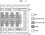
- FIG. 2 shows a layout diagram of the voltage-breakdown protecting portion of the semiconductor device according to a first embodiment.
- the voltage-breakdown protecting portion 12 is made of a transistor formed in a region surrounded by a diffusion layer on an N well.
- the drains of the PMOS transistors P3, P4 and P5 are connected to the diffusion layer surrounding the region where the transistor is formed.
- the gate of the PMOS transistor P5 is also connected to the diffusion layer surrounding the region where the transistor is formed.
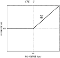
- FIG. 3 shows an explanatory graph of the operation in the semiconductor device 1 according to the first embodiment.
- the voltage of the external connection pad PAD is boosted to the voltage that is equal to or higher than the power supply voltage.
- the region where the voltage of the external connection pad PAD is equal to or lower than the power supply voltage is a regular operation region.
- the voltage of each back gate wiring FNW of the output transistor MP1 and the PMOS transistors P1 to P6 is the power supply voltage VDD.
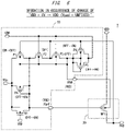
- FIG. 4 shows an explanatory circuit diagram of an operation in a case of switching the gate signal from the low level to the high level in the semiconductor device according to the first embodiment.
- FIG. 5 shows an explanatory circuit diagram of an operation in a case of switching the gate signal from the high level to the low level in the semiconductor device according to the first embodiment.
- a voltage Vpad of the external connection pad PAD is applied to the gate of the PMOS transistor P4, and the power supply voltage VDD is applied to the source of the same.
- the power supply voltage VDD is applied to the source of the PMOS transistor P5, and this transistor functions as a diode. In other words, the PMOS transistor P5 is turned ON. In this manner, the back gate wiring FNW is at the power supply voltage VDD.
- the power supply voltage VDD is applied to the gates of the PMOS transistors P2 and P3 while the voltage Vpad of the external connection pad PAD is applied to the sources of the same, and these transistors are turned OFF.
- the NMOS transistor N1 and the PMOS transistor P6 in the semiconductor device 1 are switched from the ON state to the OFF state.
- the PMOS transistor P1 is switched from the ON state to the OFF state.
- the gate wiring PGnF is switched from the low level to the high level, and the output transistor MP1 is switched from the ON state to the OFF state.
- the external connection pad PAD is switched from the high level to the low level.
- the NMOS transistor N1 and the PMOS transistor P6 in the semiconductor device 1 are switched from the OFF state to the ON state.
- the PMOS transistor P1 is switched from the ON state to the OFF state.
- the gate wiring PGnF is switched from the high level to the low level, and the output transistor MP1 is switched from the OFF state to the ON state.
- the external connection pad PAD is switched from the low level to the high level.
- the extraction of charges from the gate wiring PGnF is delayed until an ON resistance of the NMOS transistor N1 becomes low.
- the PMOS transistor P6 becomes in the low resistance state at an earlier timing than the NMOS transistor N1 since the gate of the PMOS transistor P6 is connected to the gate wiring PGnF, and therefore, the voltage drop of the gate wiring PGnF is accelerated. In other words, by the arrangement of the PMOS transistor P6, the voltage drop operation of the gate wiring PGnF can be rapidly performed.
- the voltage of the gate of the PMOS transistor P4 is unfixed since the voltage of the external connection pad PAD is unfixed. Therefore, a leakage electric current flows in the PMOS transistor P4. In this manner, the voltage of the drain of the PMOS transistor P4 changes to the power supply voltage VDD.
- the voltage of the gate of the PMOS transistor P5 is also unfixed at the time of the power ON. In this case, since the voltage of the source of the PMOS transistor P5 becomes the power supply voltage VDD, a leakage electric current flows in the PMOS transistor P5. In this manner, the voltage of the drain of the PMOS transistor P5 also changes to the power supply voltage VDD.
- FIG. 7 shows an explanatory circuit diagram of an operation in a case of the higher voltage of the external connection pad PAD than the power supply voltage in the semiconductor device according to the first embodiment.
- the PMOS transistor P4 to which the voltage Vpad is applied is turned OFF since its gate voltage is higher than the power supply voltage VDD.
- the PMOS transistors P3 and P2 are turned ON since the voltage Vpad is applied to their sources while the power supply voltage VDD is applied to their gates. In this manner, the voltages of the back gate wiring FNW and the gate wiring PGnF become the voltage Vpad of the external connection pad PAD.
- the PMOS transistors P1 and P6 are turned OFF since there is no potential difference between the source (or the drain in the regular operation region) and the gate.
- the NMOS transistor N1 is also turned OFF. In other words, the signal transmitting portion 11 disconnects the input signal from the input terminal PGn.
- each back gate voltage of the PMOS transistors P1 to P6 and the output transistor MP1 becomes the voltage Vpad of the external connection pad PAD, and each gate voltage of the PMOS transistors P1, P4, P5 and P6 and the output transistor MP1 also becomes the voltage Vpad.
- Each gate voltage of the PMOS transistors P2 and P3 becomes the power supply voltage VDD. Therefore, in the semiconductor device 1, even if the voltage Vpad is twice the power supply voltage VDD, the voltage difference between the gate and the back gate of the PMOS transistors P1 to P6 and the output transistor MP1 is only about the power supply voltage VDD, and therefore, the voltage breakdown specification of the transistor can be satisfied.
- the voltage-breakdown protecting portion 12 brings the signal transmitting portion 11 into the disconnection state, and applies the voltage of the external connection pad to the back gate and the gate of the output transistor MP1.
- the voltage breakdown specification of the transistor can be also satisfied in the case of the voltage Vpad that is about twice the power supply voltage VDD.
- the breakdown voltage of the external connection pad PAD can be made higher than the voltage value of the breakdown voltage specification of the output transistor MP1.
- the signal transmitting portion 11 and the voltage-breakdown protecting portion 12 are made of the seven transistors. However, these transistors are not used as the output-stage circuit, and therefore, do not need to have a low resistance as low as that of the output transistor MP1. Therefore, each transistor configuring the signal transmitting portion 11 and the voltage-breakdown protecting portion 12 can be achieved by a much smaller transistor than the output transistor MP1. Therefore, the chip size of the semiconductor device 1 according to the first embodiment can be made small. The larger the difference in the transistor size between the output transistor MP1 and each transistor configuring the signal transmitting portion 11 and the voltage-breakdown protecting portion 12 is, the larger the effect of the size reduction of the chip size is.
- the output-stage circuit 20 in the semiconductor device 1 according to the first embodiment can be made of a single-stage transistor, a terminal capacitance of the external connection pad PAD can be lowered. Because of the lowering of the terminal capacitance as described above, a signal having a higher frequency can be handled.
- a semiconductor device 2 according to a different embodiment from the semiconductor device 1 will be explained.
- the same components as the components explained in the first embodiment will be denoted with the same reference symbols as those of the first embodiment, and the explanation for the components will be omitted.
- FIG. 8 shows a circuit diagram of the semiconductor device 2 according to the second embodiment.
- the semiconductor device 2 according to the second embodiment includes a pre-stage circuit 10a including a signal transmitting portion 11a and a voltage-breakdown protecting portion 12a in place of the signal transmitting portion 11 and the voltage-breakdown protecting portion 12.
- the signal transmitting portion 11a is made by removal of the PMOS transistor P6 from the signal transmitting portion 11.
- the voltage-breakdown protecting portion 12a is made by removal of the PMOS transistor P5 from the voltage-breakdown protecting portion 12.
- the PMOS transistor P6 accelerates the potential drop of the gate wiring PGnF.
- the PMOS transistor P6 may be removed if the specification of the semiconductor device 2 allows the semiconductor device to be operated at a low operational speed.
- the PMOS transistor P5 assists the fixation of the voltage of the back gate wiring FNW.
- the PMOS transistor P5 may not be used if the potential of the external connection pad PAD is fixed to the ground voltage or others at the time of the power ON.
- the PMOS transistor P5 can be removed if the voltage of the external connection pad PAD is configured to be pulled down in the outside.
- the semiconductor device 2 according to the second embodiment can have the less number of transistors than that of the semiconductor device 1 and the smaller chip size than that of the first embodiment.
- a semiconductor device 3 according to a different embodiment from that of the semiconductor device 1 will be explained.
- the same components as the components explained in the first embodiment will be denoted with the same reference symbols as those of the first embodiment, and the explanation for the components will be omitted.
- FIG. 9 shows a circuit diagram of the semiconductor device according to the third embodiment.
- each of the NMOS transistor N1 and the PMOS transistors P1 to P6 is made of a thin film transistor having a thinner gate oxidation film than that of the output transistor MP1.
- the signal transmitting portion 11 and the voltage-breakdown protecting portion 12 made of the thin film transistor are illustrated as a signal transmitting portion 11b and a voltage-breakdown protecting portion 12b.
- each area of the NMOS transistor N1 and the PMOS transistors P1 to P6 on the chip can be further reduced.
- a semiconductor device 4 according to a different embodiment from that of the semiconductor device 1 will be explained.
- the same components as the components explained in the first embodiment will be denoted with the same reference symbols as those of the first embodiment, and the explanation for the components will be omitted.
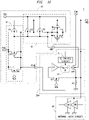
- FIG. 10 shows a circuit diagram of the semiconductor device 4 according to the fourth embodiment.
- the semiconductor device 4 according to the fourth embodiment includes an output-stage circuit 20c in place of the output-stage circuit 20.
- the output-stage circuit 20c is a regulator circuit using the output transistor MP1 as a driving transistor.
- the semiconductor device 4 according to the fourth embodiment includes an internal logic circuit 30 to supply a power to the internal logic circuit 30 from either the output-stage circuit 20c or the external power supply through the external connection pad PAD.
- the output-stage circuit 20c includes a load resistor R1, a second N-type transistor (such as NMOS transistor N2), an operational amplifier OP, a switch control circuit 21 and a switch 22 in addition to the output transistor MP1.
- a load resistor R1 is connected to the drain of the output transistor MP1, and the ground potential is applied to the other end.
- the NMOS transistor N2 is connected between an input terminal of the operational amplifier OP and one end of the load resistor R1, and the power supply voltage VDD is applied to a gate of the NMOS transistor.
- the switch 22 switches the gate of the output transistor MP1 to be connected to either an output terminal of the operational amplifier OP or the gate wiring.
- the switch control circuit 21 instructs the switch 22 to connect the gate of the output transistor MP1 to the gate wiring PGnF if the voltage Vpad of the external connection pad PAD is higher than the power supply voltage VDD.
- the switch control circuit 21 instructs the switch 22 to connect the gate of the output transistor MP1 to the output terminal of the operational amplifier OP if the voltage Vpad of the external connection pad PAD is equal to or lower than the power supply voltage VDD.
- the semiconductor device 4 if the voltage Vpad of the external connection pad PAD is higher than the power supply voltage VDD, the voltage-breakdown violation of the output transistor MP1 is avoided by the same operation as that of the semiconductor device 1 according to the first embodiment. In this case, the NMOS transistor N2 prevents the overvoltage from being applied to the input terminal of the operational amplifier OP. Meanwhile, in the semiconductor device 4, in the general operational region where the voltage Vpad of the external connection pad PAD is equal to or lower than the power supply voltage VDD, the output transistor MP1 is used as the driving transistor of the regulator.
- the driving transistor of the regulator circuit configured as the output-stage circuit 20c can be configured to be a single-stage driving transistor, and therefore, the semiconductor device 4 can more suppress the variation in the driving performance of the regulator circuit than a case of a multiple-stage driving transistor.
- a semiconductor device 5 according to a different embodiment from that of the semiconductor device 4 will be explained.
- the same components as the components explained in the first and fourth embodiments will be denoted with the same reference symbols as those of the first and fourth embodiments, and the explanation for the components will be omitted.
- FIG. 11 shows a circuit diagram of the semiconductor device 5 according to the fifth embodiment. As shown in FIG. 5 , in the semiconductor device 5 according to the fifth embodiment, an output-stage circuit 20d is used in place of the output-stage circuit 20c of the semiconductor device 4.
- the output-stage circuit 20d includes a load resistor R1, an NMOS transistor N2 and an operational amplifier OP in addition to the output transistor MP1.
- An output end of the operational amplifier OP is connected to the input terminal PGn.
- One end of the load resistor R1 is connected to the drain of the output transistor MP1, and the ground potential is applied to the other end.
- the NMOS transistor N2 is connected between an input terminal of the operational amplifier OP and one end of the load resistor R1, and the power supply voltage VDD is applied to a gate of the NMOS transistor.
- the output-stage circuit 20d is a regulator circuit supplying the power to the internal logic circuit 30 as similar to the output-stage circuit 20c.
- the pre-stage circuit 10 is configured to be sandwiched between the output terminal of the operational amplifier OP and the gate of the output transistor MP1.
- the switch control circuit 21 and the switch 22 used in the semiconductor device 4 can be removed.
- the chip size of the semiconductor device 5 can be made smaller than that of the semiconductor device 4.
Landscapes
- Engineering & Computer Science (AREA)
- Physics & Mathematics (AREA)
- Computer Hardware Design (AREA)
- Computing Systems (AREA)
- General Engineering & Computer Science (AREA)
- Mathematical Physics (AREA)
- Power Engineering (AREA)
- Semiconductor Integrated Circuits (AREA)
- Metal-Oxide And Bipolar Metal-Oxide Semiconductor Integrated Circuits (AREA)
- Logic Circuits (AREA)
Abstract
Description
- The disclosure of
Japanese Patent Application No. 2021-013055 filed on January 29, 2021 - The present invention relates to a semiconductor device, and relates to, for example, a semiconductor device including a driver circuit used for signal output.
- There are disclosed techniques listed below.
- [Patent Document 1]
Japanese Unexamined Patent Application Publication No. 2019-213122 - An output-stage circuit of the semiconductor device needs to be designed in accordance with an output impedance specification and designed to prevent electrostatic discharge (ESD) damage. In order to satisfy such design specification, it is necessary to use a large size transistor for the output-stage circuit. Accordingly, the
Patent Document 1 discloses a technique related to this output-stage circuit. - A semiconductor device described in the
Patent Document 1 is a semiconductor device connected to a first power supply voltage and a second power supply voltage that is lower than the first power supply voltage, and includes a driver circuit configured to receive an output signal as its input from a circuit operating in response to supply of the second power supply voltage and configured to output a signal having a shifted voltage level, and includes an output circuit configured to receive an output signal as its input from the driver circuit. The output circuit includes a first transistor between the first power supply voltage and an output node and a second transistor between the output node and a ground voltage. The driver circuit includes a middle-voltage generating circuit configured to receive the output signal as its input and convert the output signal to have a voltage level of a middle voltage and a signal generating circuit configured to output a driving signal for use in driving the first transistor in accordance with the middle voltage generated by the middle-voltage generating circuit. - However, the output-stage circuit described in the
Patent Document 1 has a problem of a large chip size since each size of a plurality of transistors configuring the output-stage circuit is large in order to satisfy the breakdown voltage specification. - Other objects and novel characteristics will be apparent from the description of the present specification and the accompanying drawings.
- According to an embodiment, a semiconductor device includes: a P-type output transistor configured to have a source to which a power supply voltage is applied and a drain connected to an external connection pad; a gate wiring configured to be connected to a gate of the output transistor; a signal transmitting portion configured to transmit an input signal to the gate wiring; and a voltage-breakdown protecting portion configured to apply the power supply voltage to a back gate of the output transistor if the voltage applied on the external connection pad is equal to or lower than the power supply voltage or configured to bring the signal transmitting portion into a disconnection state and apply the voltage applied on the external connection pad to the gate and the back gate of the output transistor if the voltage applied on the external connection pad is higher than the power supply voltage.
- According to the embodiment, in the semiconductor device, the breakdown voltage specification of the transistor can be satisfied along with the suppression of the chip area.
-
-
FIG. 1 is a circuit diagram of a semiconductor device according to a first embodiment. -
FIG. 2 is a layout diagram of a voltage-breakdown protecting portion of the semiconductor device according to the first embodiment. -
FIG. 3 is an explanatory graph of an operation in the semiconductor device according to the first embodiment. -
FIG. 4 is an explanatory circuit diagram of an operation in a case of switching a gate signal from a low level to a high level in the semiconductor device according to the first embodiment. -
FIG. 5 is an explanatory circuit diagram of an operation in a case of switching the gate signal from the high level to the low level in the semiconductor device according to the first embodiment. -
FIG. 6 is an explanatory circuit diagram of an operation at power ON of the semiconductor device according to the first embodiment. -
FIG. 7 is an explanatory circuit diagram of an operation in a case of a higher voltage of an explanatory connection pad than a power supply voltage in the semiconductor device according to the first embodiment. -
FIG. 8 is a circuit diagram of a semiconductor device according to a second embodiment. -
FIG. 9 is a circuit diagram of a semiconductor device according to a third embodiment. -
FIG. 10 is a circuit diagram of a semiconductor device according to a fourth embodiment. -
FIG. 11 is a circuit diagram of a semiconductor device according to a fifth embodiment. - In order to make the explanation clear, the following description and drawings are appropriately omitted or simplified. In each of the drawings, the same components are denoted with the same reference symbols, and the repetitive description thereof will be omitted if needed.
- One of features of a
semiconductor device 1 according to the first embodiment is the output-stage circuit including the transistor connected to the external connection pad and a pre-stage circuit, and therefore, the output-stage circuit and the pre-stage circuit of thesemiconductor device 1 will be explained below.FIG. 1 shows a circuit diagram of thesemiconductor device 1 according to the first embodiment. InFIG. 1 , a power supply wiring to which a power supply voltage VDD is applied is denoted with a reference symbol "VDD". The wiring inside thesemiconductor device 1 is virtually provided with a terminal.FIG. 1 shows an input terminal PGn as a virtual terminal.FIG. 1 shows terminal symbols that are a back gate wiring FNW and a gate wiring PGnF as internal wirings. Further, thesemiconductor device 1 is formed in a semiconductor chip, and includes an external connection pad PAD electrically connected to a different device out of the semiconductor chip. - As shown in
FIG. 1 , thesemiconductor device 1 includes apre-stage circuit 10 and an output-stage circuit 20. InFIG. 1 , thepre-stage circuit 10 has a function of transmitting the signals to the output-stage circuit 20 and a voltage-breakdown protecting function of avoiding the output-stage circuit 20 from the voltage-breakdown violation if a higher voltage than the power supply voltage VDD is applied to an external connection pad PAD. The output-stage circuit 20 is a circuit to be a driver for an output signal supplied out of the semiconductor chip. In the example shown inFIG. 1 , the output-stage circuit 20 includes an output transistor MP1. The output transistor MP1 is a P-type transistor (such as a PMOS transistor). The power supply voltage VDD is applied to a source of the output transistor MP1, a drain of the same is connected to the external connection pad PAD, and a gate of the same is connected to the gate wiring PGnF. A transistor configuring thepre-stage circuit 10 can be achieved by a transistor that is much smaller than the output transistor MP1. - The
pre-stage circuit 10 includes asignal transmitting portion 11 and a voltage-breakdown protecting portion 12. Thesignal transmitting portion 11 transmits an input signal (such as an input signal to the input terminal PGn) to a gate wiring. The voltage-breakdown protecting portion 12 applies the power supply voltage to a back gate of the output transistor MP1 if the voltage applied on the external connection pad PAD is equal to or lower than the power supply voltage VDD. Alternatively, the voltage-breakdown protecting portion 12 brings thesignal transmitting portion 11 into a disconnection state, and applies the voltage applied on the external connection pad PAD to the gate and the back gate of the output transistor MP1 if the voltage applied on the external connection pad PAD is higher than the power supply voltage VDD. - The
signal transmitting portion 11 includes a first N-type transistor (such as a NMOS transistor N1), a first P-type transistor (such as a PMOS transistor P1) and a sixth P-type transistor (such as a PMOS transistor P6). The voltage-breakdown protecting portion 12 includes a second P-type transistor (such as a PMOS transistor P2), a third P-type transistor (such as a PMOS transistor P3), a fourth P-type transistor (such as a PMOS transistor P4), and a fifth P-type transistor (such as a PMOS transistor P5). To the input terminal PGn, a gate signal (such as an input signal) having a voltage level of either the ground voltage or the power supply voltage VDD is input. In the transistor, the source and the drain are switched by the voltage applied to the back gate. In the following explanation, a source and a drain in a state in which the voltage of the external connection pad PAD is equal to or lower than the power supply voltage VDD are referred to as the source and the drain of each transistor. - A source of the NMOS transistor N1 is connected to the input terminal PGn, the power supply voltage VDD is applied to a gate of the same, and a drain of the same is connected to the gate wiring PGnF. A back gate of the NMOS transistor N1 is connected to the source of the NMOS transistor N1. A source of the PMOS transistor P1 is connected to the input terminal PGn, a gate of the same is connected to the external connection pad PAD, and a drain of the same is connected to the gate wiring PGnF. A source of the PMOS transistor P6 is connected to the input terminal PGn, a gate and a drain of the same are commonly connected, and the drain of the same is connected to the gate wiring PGnF.
- The power supply voltage VDD is applied to a gate of the PMOS transistor P2, a drain of the same is connected to the gate wiring PGnF, and a source of the same is connected to the external connection pad PAD. The power supply voltage VDD is applied to a gate of the PMOS transistor P3, and a source of the same is connected to the external connection pad PAD. The power supply voltage VDD is applied to a source of the PMOS transistor P4, a gate of the same is connected to the external connection pad PAD, and a drain of the same is connected to the drain of the PMOS transistor P3. The power supply voltage VDD is applied to a source of the PMOS transistor P5, a gate and a drain of the same are commonly connected, and the drain of the same is connected to the PMOS transistor P3.
- In the
semiconductor device 1, the back gates of the PMOS transistors P1 to P6 and the output transistor MP1 are commonly connected to the drains of the PMOS transistors P4 and P5. A layout of the voltage-breakdown protecting portion 12 having such a connection between the drain and the back gate will be explained. Accordingly,FIG. 2 shows a layout diagram of the voltage-breakdown protecting portion of the semiconductor device according to a first embodiment. - As shown in
FIG. 2 , the voltage-breakdown protecting portion 12 is made of a transistor formed in a region surrounded by a diffusion layer on an N well. By a wiring, the drains of the PMOS transistors P3, P4 and P5 are connected to the diffusion layer surrounding the region where the transistor is formed. The gate of the PMOS transistor P5 is also connected to the diffusion layer surrounding the region where the transistor is formed. - Next, an operation in the
semiconductor device 1 according to the first embodiment will be explained. First,FIG. 3 shows an explanatory graph of the operation in thesemiconductor device 1 according to the first embodiment. In the example shown inFIG. 3 , in a state in which the input signal to be input to the input terminal PGn is at a high level while the gate wiring PGnF is at a high level, the voltage of the external connection pad PAD is boosted to the voltage that is equal to or higher than the power supply voltage. - As shown in
FIG. 3 , in thesemiconductor device 1 according to the first embodiment, the region where the voltage of the external connection pad PAD is equal to or lower than the power supply voltage is a regular operation region. In this regular operation region, the voltage of each back gate wiring FNW of the output transistor MP1 and the PMOS transistors P1 to P6 is the power supply voltage VDD. - On the other hand, when the higher voltage than the power supply voltage VDD is applied to the external connection pad PAD, the voltage of each of the gate wiring PGnF and the back gate wiring FNW of the
semiconductor device 1 is boosted to follow the voltage of the external connection pad PAD. Such a voltage following operation is achieved by the operation of the voltage-breakdown protecting portion 12. Therefore, with reference to the circuit drawings, the operation of thesemiconductor device 1 will be explained. - An operation of the regular operation region will be explained with reference to
FIGs. 4 to 6 , and an operation of an overvoltage application region where a higher voltage than the power supply voltage VDD is applied to the external connection pad PAD will be explained with reference toFIG. 7 . - First,
FIG. 4 shows an explanatory circuit diagram of an operation in a case of switching the gate signal from the low level to the high level in the semiconductor device according to the first embodiment.FIG. 5 shows an explanatory circuit diagram of an operation in a case of switching the gate signal from the high level to the low level in the semiconductor device according to the first embodiment. - As shown in
FIGs. 4 and5 , in the regular operation region of thesemiconductor device 1, a voltage Vpad of the external connection pad PAD is applied to the gate of the PMOS transistor P4, and the power supply voltage VDD is applied to the source of the same. The power supply voltage VDD is applied to the source of the PMOS transistor P5, and this transistor functions as a diode. In other words, the PMOS transistor P5 is turned ON. In this manner, the back gate wiring FNW is at the power supply voltage VDD. And, the power supply voltage VDD is applied to the gates of the PMOS transistors P2 and P3 while the voltage Vpad of the external connection pad PAD is applied to the sources of the same, and these transistors are turned OFF. - As shown in
FIG. 4 , when the input signal changes from the low level to the high level, the NMOS transistor N1 and the PMOS transistor P6 in thesemiconductor device 1 are switched from the ON state to the OFF state. The PMOS transistor P1 is switched from the ON state to the OFF state. In this manner, the gate wiring PGnF is switched from the low level to the high level, and the output transistor MP1 is switched from the ON state to the OFF state. The external connection pad PAD is switched from the high level to the low level. - As shown in
FIG. 5 , when the input signal changes from the high level to the low level, the NMOS transistor N1 and the PMOS transistor P6 in thesemiconductor device 1 are switched from the OFF state to the ON state. The PMOS transistor P1 is switched from the ON state to the OFF state. In this manner, the gate wiring PGnF is switched from the high level to the low level, and the output transistor MP1 is switched from the OFF state to the ON state. The external connection pad PAD is switched from the low level to the high level. - When the NMOS transistor N1 changes from the OFF state to the ON state, the extraction of charges from the gate wiring PGnF is delayed until an ON resistance of the NMOS transistor N1 becomes low. In this case, the PMOS transistor P6 becomes in the low resistance state at an earlier timing than the NMOS transistor N1 since the gate of the PMOS transistor P6 is connected to the gate wiring PGnF, and therefore, the voltage drop of the gate wiring PGnF is accelerated. In other words, by the arrangement of the PMOS transistor P6, the voltage drop operation of the gate wiring PGnF can be rapidly performed.
- Next, an operation of the
semiconductor device 1 at the time of power-ON in a state in which the external connection pad PAD is open and has an unfixed voltage state will be explained. - As shown in
FIG. 6 , when the power supply voltage changes from 0 V to the power supply voltage VDD, the voltage of the gate of the PMOS transistor P4 is unfixed since the voltage of the external connection pad PAD is unfixed. Therefore, a leakage electric current flows in the PMOS transistor P4. In this manner, the voltage of the drain of the PMOS transistor P4 changes to the power supply voltage VDD. The voltage of the gate of the PMOS transistor P5 is also unfixed at the time of the power ON. In this case, since the voltage of the source of the PMOS transistor P5 becomes the power supply voltage VDD, a leakage electric current flows in the PMOS transistor P5. In this manner, the voltage of the drain of the PMOS transistor P5 also changes to the power supply voltage VDD. - In this manner, by the arrangement of the PMOS transistor P5, a leakage electric current in a case of an unfixed voltage Vpad of the external connection pad PAD is made more than that of the arrangement of only the PMOS transistor P4. Therefore, the voltage of the back gate wiring FNW can be made earlier to be fixed to the power supply voltage VDD.
- Next, an operation of the
semiconductor device 1 in the overvoltage application region where the voltage Vpad of the external connection pad PAD is equal to or higher than the power supply voltage VDD will be explained. Therefore,FIG. 7 shows an explanatory circuit diagram of an operation in a case of the higher voltage of the external connection pad PAD than the power supply voltage in the semiconductor device according to the first embodiment. - As shown in
FIG. 7 , in the case of the higher voltage Vpad of the external connection pad PAD than the power supply voltage VDD, the PMOS transistor P4 to which the voltage Vpad is applied is turned OFF since its gate voltage is higher than the power supply voltage VDD. On the other hand, the PMOS transistors P3 and P2 are turned ON since the voltage Vpad is applied to their sources while the power supply voltage VDD is applied to their gates. In this manner, the voltages of the back gate wiring FNW and the gate wiring PGnF become the voltage Vpad of the external connection pad PAD. - The PMOS transistors P1 and P6 are turned OFF since there is no potential difference between the source (or the drain in the regular operation region) and the gate. The NMOS transistor N1 is also turned OFF. In other words, the
signal transmitting portion 11 disconnects the input signal from the input terminal PGn. - In this case, as shown in
FIG. 7 , in the overvoltage application region, each back gate voltage of the PMOS transistors P1 to P6 and the output transistor MP1 becomes the voltage Vpad of the external connection pad PAD, and each gate voltage of the PMOS transistors P1, P4, P5 and P6 and the output transistor MP1 also becomes the voltage Vpad. Each gate voltage of the PMOS transistors P2 and P3 becomes the power supply voltage VDD. Therefore, in thesemiconductor device 1, even if the voltage Vpad is twice the power supply voltage VDD, the voltage difference between the gate and the back gate of the PMOS transistors P1 to P6 and the output transistor MP1 is only about the power supply voltage VDD, and therefore, the voltage breakdown specification of the transistor can be satisfied. - The above-described explanation shows that, if the voltage of the external connection pad is higher than the power supply voltage in the
semiconductor device 1 according to the first embodiment, the voltage-breakdown protecting portion 12 brings thesignal transmitting portion 11 into the disconnection state, and applies the voltage of the external connection pad to the back gate and the gate of the output transistor MP1. In this manner, in thesemiconductor device 1 according to the first embodiment, even if the number of stages of the output transistor MP1 of the output-stage circuit 20 is one, the voltage breakdown specification of the transistor can be also satisfied in the case of the voltage Vpad that is about twice the power supply voltage VDD. In other words, in thesemiconductor device 1 according to the first embodiment, the breakdown voltage of the external connection pad PAD can be made higher than the voltage value of the breakdown voltage specification of the output transistor MP1. - The
signal transmitting portion 11 and the voltage-breakdown protecting portion 12 are made of the seven transistors. However, these transistors are not used as the output-stage circuit, and therefore, do not need to have a low resistance as low as that of the output transistor MP1. Therefore, each transistor configuring thesignal transmitting portion 11 and the voltage-breakdown protecting portion 12 can be achieved by a much smaller transistor than the output transistor MP1. Therefore, the chip size of thesemiconductor device 1 according to the first embodiment can be made small. The larger the difference in the transistor size between the output transistor MP1 and each transistor configuring thesignal transmitting portion 11 and the voltage-breakdown protecting portion 12 is, the larger the effect of the size reduction of the chip size is. - Since the output-
stage circuit 20 in thesemiconductor device 1 according to the first embodiment can be made of a single-stage transistor, a terminal capacitance of the external connection pad PAD can be lowered. Because of the lowering of the terminal capacitance as described above, a signal having a higher frequency can be handled. - In a second embodiment, a
semiconductor device 2 according to a different embodiment from thesemiconductor device 1 will be explained. In the explanation of the second embodiment, the same components as the components explained in the first embodiment will be denoted with the same reference symbols as those of the first embodiment, and the explanation for the components will be omitted. -
FIG. 8 shows a circuit diagram of thesemiconductor device 2 according to the second embodiment. As shown inFIG. 8 , thesemiconductor device 2 according to the second embodiment includes apre-stage circuit 10a including asignal transmitting portion 11a and a voltage-breakdown protecting portion 12a in place of thesignal transmitting portion 11 and the voltage-breakdown protecting portion 12. Thesignal transmitting portion 11a is made by removal of the PMOS transistor P6 from thesignal transmitting portion 11. The voltage-breakdown protecting portion 12a is made by removal of the PMOS transistor P5 from the voltage-breakdown protecting portion 12. - The PMOS transistor P6 accelerates the potential drop of the gate wiring PGnF. However, the PMOS transistor P6 may be removed if the specification of the
semiconductor device 2 allows the semiconductor device to be operated at a low operational speed. And, when the voltage Vpad of the external connection pad PAD is unfixed at the time of the power ON, the PMOS transistor P5 assists the fixation of the voltage of the back gate wiring FNW. However, the PMOS transistor P5 may not be used if the potential of the external connection pad PAD is fixed to the ground voltage or others at the time of the power ON. For example, the PMOS transistor P5 can be removed if the voltage of the external connection pad PAD is configured to be pulled down in the outside. - The above-described explanation shows that the
semiconductor device 2 according to the second embodiment can have the less number of transistors than that of thesemiconductor device 1 and the smaller chip size than that of the first embodiment. - In a third embodiment, a
semiconductor device 3 according to a different embodiment from that of thesemiconductor device 1 will be explained. In the explanation of the third embodiment, the same components as the components explained in the first embodiment will be denoted with the same reference symbols as those of the first embodiment, and the explanation for the components will be omitted. -
FIG. 9 shows a circuit diagram of the semiconductor device according to the third embodiment. As shown inFIG. 9 , in thesemiconductor device 3 according to the third embodiment, each of the NMOS transistor N1 and the PMOS transistors P1 to P6 is made of a thin film transistor having a thinner gate oxidation film than that of the output transistor MP1. InFIG. 9 , thesignal transmitting portion 11 and the voltage-breakdown protecting portion 12 made of the thin film transistor are illustrated as asignal transmitting portion 11b and a voltage-breakdown protecting portion 12b. - Since the thin film transistor is used as described above, each area of the NMOS transistor N1 and the PMOS transistors P1 to P6 on the chip can be further reduced.
- In a fourth embodiment, a
semiconductor device 4 according to a different embodiment from that of thesemiconductor device 1 will be explained. In the explanation of the fourth embodiment, the same components as the components explained in the first embodiment will be denoted with the same reference symbols as those of the first embodiment, and the explanation for the components will be omitted. -
FIG. 10 shows a circuit diagram of thesemiconductor device 4 according to the fourth embodiment. As shown inFIG. 10 , thesemiconductor device 4 according to the fourth embodiment includes an output-stage circuit 20c in place of the output-stage circuit 20. The output-stage circuit 20c is a regulator circuit using the output transistor MP1 as a driving transistor. And, thesemiconductor device 4 according to the fourth embodiment includes aninternal logic circuit 30 to supply a power to theinternal logic circuit 30 from either the output-stage circuit 20c or the external power supply through the external connection pad PAD. - The output-
stage circuit 20c includes a load resistor R1, a second N-type transistor (such as NMOS transistor N2), an operational amplifier OP, aswitch control circuit 21 and a switch 22 in addition to the output transistor MP1. One end of the load resistor R1 is connected to the drain of the output transistor MP1, and the ground potential is applied to the other end. The NMOS transistor N2 is connected between an input terminal of the operational amplifier OP and one end of the load resistor R1, and the power supply voltage VDD is applied to a gate of the NMOS transistor. The switch 22 switches the gate of the output transistor MP1 to be connected to either an output terminal of the operational amplifier OP or the gate wiring. Theswitch control circuit 21 instructs the switch 22 to connect the gate of the output transistor MP1 to the gate wiring PGnF if the voltage Vpad of the external connection pad PAD is higher than the power supply voltage VDD. Alternatively, theswitch control circuit 21 instructs the switch 22 to connect the gate of the output transistor MP1 to the output terminal of the operational amplifier OP if the voltage Vpad of the external connection pad PAD is equal to or lower than the power supply voltage VDD. - In the
semiconductor device 4 according to the fourth embodiment, if the voltage Vpad of the external connection pad PAD is higher than the power supply voltage VDD, the voltage-breakdown violation of the output transistor MP1 is avoided by the same operation as that of thesemiconductor device 1 according to the first embodiment. In this case, the NMOS transistor N2 prevents the overvoltage from being applied to the input terminal of the operational amplifier OP. Meanwhile, in thesemiconductor device 4, in the general operational region where the voltage Vpad of the external connection pad PAD is equal to or lower than the power supply voltage VDD, the output transistor MP1 is used as the driving transistor of the regulator. - In the
semiconductor device 4 according to the fourth embodiment, the driving transistor of the regulator circuit configured as the output-stage circuit 20c can be configured to be a single-stage driving transistor, and therefore, thesemiconductor device 4 can more suppress the variation in the driving performance of the regulator circuit than a case of a multiple-stage driving transistor. - In a fifth embodiment, a
semiconductor device 5 according to a different embodiment from that of thesemiconductor device 4 will be explained. In the explanation of the fifth embodiment, the same components as the components explained in the first and fourth embodiments will be denoted with the same reference symbols as those of the first and fourth embodiments, and the explanation for the components will be omitted. -
FIG. 11 shows a circuit diagram of thesemiconductor device 5 according to the fifth embodiment. As shown inFIG. 5 , in thesemiconductor device 5 according to the fifth embodiment, an output-stage circuit 20d is used in place of the output-stage circuit 20c of thesemiconductor device 4. - The output-
stage circuit 20d includes a load resistor R1, an NMOS transistor N2 and an operational amplifier OP in addition to the output transistor MP1. An output end of the operational amplifier OP is connected to the input terminal PGn. One end of the load resistor R1 is connected to the drain of the output transistor MP1, and the ground potential is applied to the other end. The NMOS transistor N2 is connected between an input terminal of the operational amplifier OP and one end of the load resistor R1, and the power supply voltage VDD is applied to a gate of the NMOS transistor. In other words, the output-stage circuit 20d is a regulator circuit supplying the power to theinternal logic circuit 30 as similar to the output-stage circuit 20c. In the out-stage circuit 20d in this case, thepre-stage circuit 10 is configured to be sandwiched between the output terminal of the operational amplifier OP and the gate of the output transistor MP1. - In this manner, in the fifth embodiment, the
switch control circuit 21 and the switch 22 used in thesemiconductor device 4 can be removed. By the simplified circuit as described above, the chip size of thesemiconductor device 5 can be made smaller than that of thesemiconductor device 4. - In the foregoing, the invention made by the present inventors has been concretely described on the basis of the embodiments. However, it is needless to say that the present invention is not limited to the foregoing embodiments, and various modifications can be made within the scope of the present invention.
Claims (7)
- A semiconductor device comprising:a P-type output transistor configured to have a source to which a power supply voltage is applied, and a drain connected to an external connection pad;a gate wiring configured to be connected to a gate of the output transistor;a signal transmitting portion configured to transmit an input signal to the gate wiring; anda voltage-breakdown protecting portion,wherein the voltage-breakdown protecting portion applies the power supply voltage to a back gate of the output transistor if a voltage applied on the external connection pad is equal to or lower than the power supply voltage, orthe voltage-breakdown protecting portion brings the signal transmitting portion into a disconnection state and applies the voltage on the external connection pad to the gate and the back gate of the output transistor if the voltage applied on the external connection pad is higher than the power supply voltage.
- The semiconductor device according to claim 1, comprising:a P-type output transistor configured to have a source to which a power supply voltage is applied, a drain connected to an external connection pad, and a gate connected to a gate wiring;a first N-type transistor configured to have a source connected to an input terminal to which a gate signal having a voltage level of either a ground voltage or the power supply voltage is input, a gate to which the power supply voltage is applied, and a drain connected to the gate wiring;a first P-type transistor configured to have a source connected to the input terminal, a gate connected to the external connection pad, and a drain connected to the gate wiring;a second P-type transistor configured to have a gate to which the power supply voltage is applied, a drain connected to the gate wiring, and a source connected to the external connection pad;a third P-type transistor configured to have a gate to which the power supply voltage is applied, and a source connected to the external connection pad; anda fourth P-type transistor configured to have a source to which the power supply voltage is applied, a gate connected to the external connection pad, and a drain connected to the drain of the third P-type transistor,wherein each back gate of the output transistor, the first P-type transistor, the second P-type transistor, the third P-type transistor and the fourth P-type transistor is connected to the drain of the fourth P-type transistor.
- The semiconductor device according to claim 2 further comprising
a fifth P-type transistor configured to have a source to which the power supply voltage is applied, a gate and a drain commonly connected, and the drain connected to the drain of the third P-type transistor. - The semiconductor device according to claim 2 or 3 further comprising
a sixth P-type transistor configured to have a source connected to the input terminal, a gate and a drain commonly connected, and the drain connected to the gate wiring. - The semiconductor device according to any one of claims 2 to 4,
wherein each gate oxidation film of the first N-type transistor, the first P-type transistor, the second P-type transistor, the third P-type transistor and the fourth P-type transistor is thinner than that of the output transistor. - The semiconductor device according to any one of claims 2 to 5 further comprisingan operational amplifier;a load resistor configured to have one end connected to the drain of the output transistor and the other end to which the ground voltage is applied;a second N-type transistor configured to be connected between an input terminal of the operational amplifier and one end of the load resistor, and configured to have a gate to which the power supply voltage is applied;a switch configured to switch the gate of the output transistor to be connected to either an output terminal of the operational amplifier or the gate wiring; anda switch control circuit configured to instruct the switch to connect the gate of the output transistor to the gate wiring if a voltage of the external connection pad is higher than the power supply voltage, or instruct the switch to connect the gate of the output transistor to the output terminal of the operational amplifier if the voltage of the external connection pad is equal to or lower than the power supply voltage.
- The semiconductor device according to any one of claims 2 to 5 further comprising:an operational amplifier configured to have an output end connected to the input terminal;a load resistor configured to have one end connected to the drain of the output transistor, and the other end to which the ground voltage is applied; anda second N-type transistor configured to be connected between an input terminal of the operational amplifier and one end of the load resistor, and configured to have a gate to which the power supply voltage is applied.
Applications Claiming Priority (1)
| Application Number | Priority Date | Filing Date | Title |
|---|---|---|---|
| JP2021013055A JP2022116735A (en) | 2021-01-29 | 2021-01-29 | Semiconductor device |
Publications (2)
| Publication Number | Publication Date |
|---|---|
| EP4036971A1 true EP4036971A1 (en) | 2022-08-03 |
| EP4036971B1 EP4036971B1 (en) | 2025-06-11 |
Family
ID=80035258
Family Applications (1)
| Application Number | Title | Priority Date | Filing Date |
|---|---|---|---|
| EP22153085.0A Active EP4036971B1 (en) | 2021-01-29 | 2022-01-25 | Semiconductor device |
Country Status (4)
| Country | Link |
|---|---|
| US (1) | US11843371B2 (en) |
| EP (1) | EP4036971B1 (en) |
| JP (1) | JP2022116735A (en) |
| CN (1) | CN114826240A (en) |
Citations (6)
| Publication number | Priority date | Publication date | Assignee | Title |
|---|---|---|---|---|
| US5635860A (en) * | 1995-12-28 | 1997-06-03 | Lucent Technologies Inc. | Overvoltage-tolerant self-biasing CMOS output buffer |
| US5844425A (en) * | 1996-07-19 | 1998-12-01 | Quality Semiconductor, Inc. | CMOS tristate output buffer with having overvoltage protection and increased stability against bus voltage variations |
| US6118301A (en) * | 1998-05-26 | 2000-09-12 | Analog Devices, Inc. | High voltage tolerant and compliant driver circuit |
| US6265926B1 (en) * | 1998-05-27 | 2001-07-24 | Altera Corporation | Programmable PCI overvoltage input clamp |
| US20030117174A1 (en) * | 1996-05-28 | 2003-06-26 | Altera Corporation, A Corporation Of Delaware | Programmable logic with lower internal voltage circuitry |
| JP2019213122A (en) | 2018-06-07 | 2019-12-12 | ルネサスエレクトロニクス株式会社 | Semiconductor device |
Family Cites Families (17)
| Publication number | Priority date | Publication date | Assignee | Title |
|---|---|---|---|---|
| JP3460519B2 (en) * | 1997-07-18 | 2003-10-27 | 株式会社デンソー | Buffer circuit |
| US6580411B1 (en) * | 1998-04-28 | 2003-06-17 | Sharp Kabushiki Kaisha | Latch circuit, shift register circuit and image display device operated with a low consumption of power |
| JP2000209042A (en) * | 1999-01-19 | 2000-07-28 | Nippon Telegr & Teleph Corp <Ntt> | Amplifier circuit and mixer circuit |
| JP3394509B2 (en) * | 1999-08-06 | 2003-04-07 | 株式会社リコー | Constant voltage power supply |
| JP2003031672A (en) * | 2001-07-19 | 2003-01-31 | Matsushita Electric Ind Co Ltd | Semiconductor integrated circuit device |
| JP4568096B2 (en) * | 2004-11-25 | 2010-10-27 | Okiセミコンダクタ株式会社 | Input/Output Circuit |
| JP5050628B2 (en) * | 2007-04-26 | 2012-10-17 | ミツミ電機株式会社 | Semiconductor device |
| JP2009252259A (en) * | 2008-04-01 | 2009-10-29 | Sony Corp | Semiconductor memory device |
| JP5285773B2 (en) * | 2009-06-02 | 2013-09-11 | パナソニック株式会社 | Input/Output Circuit |
| US8816722B2 (en) * | 2010-09-13 | 2014-08-26 | Semiconductor Energy Laboratory Co., Ltd. | Current detection circuit |
| KR20120121586A (en) * | 2011-04-27 | 2012-11-06 | 엘지디스플레이 주식회사 | Display device |
| JP5845160B2 (en) * | 2012-09-26 | 2016-01-20 | ルネサスエレクトロニクス株式会社 | Semiconductor device |
| CN104965555B (en) * | 2015-06-23 | 2018-11-16 | 北京兆易创新科技股份有限公司 | Voltage regulating device and voltage generate system |
| JP2018139346A (en) * | 2017-02-24 | 2018-09-06 | ルネサスエレクトロニクス株式会社 | Semiconductor device and electronic control system comprising the same |
| CN107608440A (en) * | 2017-10-25 | 2018-01-19 | 北京智芯微电子科技有限公司 | A kind of Fiducial reference source circuit with gap |
| EP3832699B1 (en) * | 2018-09-21 | 2025-03-05 | Sony Semiconductor Solutions Corporation | Semiconductor element and electronic circuit |
| CN211406369U (en) * | 2019-12-31 | 2020-09-01 | 上海鸣涵电子科技有限公司 | Security protection LED control circuit and chip that is shaded |
-
2021
- 2021-01-29 JP JP2021013055A patent/JP2022116735A/en active Pending
- 2021-12-23 US US17/560,690 patent/US11843371B2/en active Active
-
2022
- 2022-01-11 CN CN202210027889.7A patent/CN114826240A/en active Pending
- 2022-01-25 EP EP22153085.0A patent/EP4036971B1/en active Active
Patent Citations (6)
| Publication number | Priority date | Publication date | Assignee | Title |
|---|---|---|---|---|
| US5635860A (en) * | 1995-12-28 | 1997-06-03 | Lucent Technologies Inc. | Overvoltage-tolerant self-biasing CMOS output buffer |
| US20030117174A1 (en) * | 1996-05-28 | 2003-06-26 | Altera Corporation, A Corporation Of Delaware | Programmable logic with lower internal voltage circuitry |
| US5844425A (en) * | 1996-07-19 | 1998-12-01 | Quality Semiconductor, Inc. | CMOS tristate output buffer with having overvoltage protection and increased stability against bus voltage variations |
| US6118301A (en) * | 1998-05-26 | 2000-09-12 | Analog Devices, Inc. | High voltage tolerant and compliant driver circuit |
| US6265926B1 (en) * | 1998-05-27 | 2001-07-24 | Altera Corporation | Programmable PCI overvoltage input clamp |
| JP2019213122A (en) | 2018-06-07 | 2019-12-12 | ルネサスエレクトロニクス株式会社 | Semiconductor device |
Also Published As
| Publication number | Publication date |
|---|---|
| US20220247405A1 (en) | 2022-08-04 |
| CN114826240A (en) | 2022-07-29 |
| US11843371B2 (en) | 2023-12-12 |
| JP2022116735A (en) | 2022-08-10 |
| EP4036971B1 (en) | 2025-06-11 |
Similar Documents
| Publication | Publication Date | Title |
|---|---|---|
| US5532621A (en) | Output buffer circuit, input buffer circuit and bi-directional buffer circuit for plural voltage systems | |
| US5635861A (en) | Off chip driver circuit | |
| KR101926607B1 (en) | Clamping Circuit, Semiconductor having the same and Clamping method thereof | |
| US9479154B2 (en) | Semiconductor integrated circuit | |
| US8098090B2 (en) | Open-drain output buffer for single-voltage-supply CMOS | |
| JPH04290008A (en) | Off-chip-driver circuit | |
| US5635860A (en) | Overvoltage-tolerant self-biasing CMOS output buffer | |
| US6492686B1 (en) | Integrated circuit having buffering circuitry with slew rate control | |
| JPH05243974A (en) | Method for protecting output of low voltage circuit from high programming voltage | |
| CN105575960B (en) | Method and circuit for on-chip electrostatic discharge protection scheme | |
| US7606082B2 (en) | Semiconductor circuit, inverter circuit, semiconductor apparatus, and manufacturing method thereof | |
| JP7224935B2 (en) | semiconductor equipment | |
| EP4036971B1 (en) | Semiconductor device | |
| KR100304675B1 (en) | Pull up and puu down circuit | |
| US20090097176A1 (en) | Esd protection circuit and semiconductor device | |
| JP2021022666A (en) | Electrostatic protection circuit | |
| JP2021022687A (en) | Electrostatic protection circuit | |
| JP2005136088A (en) | Semiconductor integrated circuit | |
| EP3128516A1 (en) | Apparatus for performing signal driving in an electronic device with aid of different types of decoupling capacitors for pre-driver and post-driver | |
| JPH11317652A (en) | Output circuit | |
| JP4542638B2 (en) | System that controls the amount of current | |
| US12381559B2 (en) | Input/output circuit | |
| EP4456432A1 (en) | Interface device and dynamic tracking bias circuit | |
| US11742848B1 (en) | High-voltage transmission gate architecture | |
| JP3204118B2 (en) | Internal protection circuit for CMOS integrated circuit |
Legal Events
| Date | Code | Title | Description |
|---|---|---|---|
| PUAI | Public reference made under article 153(3) epc to a published international application that has entered the european phase |
Free format text: ORIGINAL CODE: 0009012 |
|
| STAA | Information on the status of an ep patent application or granted ep patent |
Free format text: STATUS: THE APPLICATION HAS BEEN PUBLISHED |
|
| AK | Designated contracting states |
Kind code of ref document: A1 Designated state(s): AL AT BE BG CH CY CZ DE DK EE ES FI FR GB GR HR HU IE IS IT LI LT LU LV MC MK MT NL NO PL PT RO RS SE SI SK SM TR |
|
| STAA | Information on the status of an ep patent application or granted ep patent |
Free format text: STATUS: REQUEST FOR EXAMINATION WAS MADE |
|
| 17P | Request for examination filed |
Effective date: 20230127 |
|
| RBV | Designated contracting states (corrected) |
Designated state(s): AL AT BE BG CH CY CZ DE DK EE ES FI FR GB GR HR HU IE IS IT LI LT LU LV MC MK MT NL NO PL PT RO RS SE SI SK SM TR |
|
| GRAP | Despatch of communication of intention to grant a patent |
Free format text: ORIGINAL CODE: EPIDOSNIGR1 |
|
| STAA | Information on the status of an ep patent application or granted ep patent |
Free format text: STATUS: GRANT OF PATENT IS INTENDED |
|
| INTG | Intention to grant announced |
Effective date: 20250107 |
|
| GRAS | Grant fee paid |
Free format text: ORIGINAL CODE: EPIDOSNIGR3 |
|
| GRAA | (expected) grant |
Free format text: ORIGINAL CODE: 0009210 |
|
| STAA | Information on the status of an ep patent application or granted ep patent |
Free format text: STATUS: THE PATENT HAS BEEN GRANTED |
|
| AK | Designated contracting states |
Kind code of ref document: B1 Designated state(s): AL AT BE BG CH CY CZ DE DK EE ES FI FR GB GR HR HU IE IS IT LI LT LU LV MC MK MT NL NO PL PT RO RS SE SI SK SM TR |
|
| REG | Reference to a national code |
Ref country code: GB Ref legal event code: FG4D |
|
| REG | Reference to a national code |
Ref country code: IE Ref legal event code: FG4D |
|
| REG | Reference to a national code |
Ref country code: DE Ref legal event code: R096 Ref document number: 602022015689 Country of ref document: DE |
|
| PG25 | Lapsed in a contracting state [announced via postgrant information from national office to epo] |
Ref country code: FI Free format text: LAPSE BECAUSE OF FAILURE TO SUBMIT A TRANSLATION OF THE DESCRIPTION OR TO PAY THE FEE WITHIN THE PRESCRIBED TIME-LIMIT Effective date: 20250611 Ref country code: ES Free format text: LAPSE BECAUSE OF FAILURE TO SUBMIT A TRANSLATION OF THE DESCRIPTION OR TO PAY THE FEE WITHIN THE PRESCRIBED TIME-LIMIT Effective date: 20250611 |
|
| REG | Reference to a national code |
Ref country code: LT Ref legal event code: MG9D |
|
| PG25 | Lapsed in a contracting state [announced via postgrant information from national office to epo] |
Ref country code: NO Free format text: LAPSE BECAUSE OF FAILURE TO SUBMIT A TRANSLATION OF THE DESCRIPTION OR TO PAY THE FEE WITHIN THE PRESCRIBED TIME-LIMIT Effective date: 20250911 Ref country code: GR Free format text: LAPSE BECAUSE OF FAILURE TO SUBMIT A TRANSLATION OF THE DESCRIPTION OR TO PAY THE FEE WITHIN THE PRESCRIBED TIME-LIMIT Effective date: 20250912 |
|
| REG | Reference to a national code |
Ref country code: NL Ref legal event code: MP Effective date: 20250611 |
|
| PG25 | Lapsed in a contracting state [announced via postgrant information from national office to epo] |
Ref country code: BG Free format text: LAPSE BECAUSE OF FAILURE TO SUBMIT A TRANSLATION OF THE DESCRIPTION OR TO PAY THE FEE WITHIN THE PRESCRIBED TIME-LIMIT Effective date: 20250611 |
|
| PG25 | Lapsed in a contracting state [announced via postgrant information from national office to epo] |
Ref country code: HR Free format text: LAPSE BECAUSE OF FAILURE TO SUBMIT A TRANSLATION OF THE DESCRIPTION OR TO PAY THE FEE WITHIN THE PRESCRIBED TIME-LIMIT Effective date: 20250611 |
|
| PG25 | Lapsed in a contracting state [announced via postgrant information from national office to epo] |
Ref country code: RS Free format text: LAPSE BECAUSE OF FAILURE TO SUBMIT A TRANSLATION OF THE DESCRIPTION OR TO PAY THE FEE WITHIN THE PRESCRIBED TIME-LIMIT Effective date: 20250911 |
|
| PG25 | Lapsed in a contracting state [announced via postgrant information from national office to epo] |
Ref country code: LV Free format text: LAPSE BECAUSE OF FAILURE TO SUBMIT A TRANSLATION OF THE DESCRIPTION OR TO PAY THE FEE WITHIN THE PRESCRIBED TIME-LIMIT Effective date: 20250611 |
|
| PG25 | Lapsed in a contracting state [announced via postgrant information from national office to epo] |
Ref country code: NL Free format text: LAPSE BECAUSE OF FAILURE TO SUBMIT A TRANSLATION OF THE DESCRIPTION OR TO PAY THE FEE WITHIN THE PRESCRIBED TIME-LIMIT Effective date: 20250611 |
|
| PG25 | Lapsed in a contracting state [announced via postgrant information from national office to epo] |
Ref country code: PT Free format text: LAPSE BECAUSE OF FAILURE TO SUBMIT A TRANSLATION OF THE DESCRIPTION OR TO PAY THE FEE WITHIN THE PRESCRIBED TIME-LIMIT Effective date: 20251013 |
|
| REG | Reference to a national code |
Ref country code: AT Ref legal event code: MK05 Ref document number: 1802965 Country of ref document: AT Kind code of ref document: T Effective date: 20250611 |
|
| PG25 | Lapsed in a contracting state [announced via postgrant information from national office to epo] |
Ref country code: IS Free format text: LAPSE BECAUSE OF FAILURE TO SUBMIT A TRANSLATION OF THE DESCRIPTION OR TO PAY THE FEE WITHIN THE PRESCRIBED TIME-LIMIT Effective date: 20251011 |
|
| PG25 | Lapsed in a contracting state [announced via postgrant information from national office to epo] |
Ref country code: AT Free format text: LAPSE BECAUSE OF FAILURE TO SUBMIT A TRANSLATION OF THE DESCRIPTION OR TO PAY THE FEE WITHIN THE PRESCRIBED TIME-LIMIT Effective date: 20250611 Ref country code: SM Free format text: LAPSE BECAUSE OF FAILURE TO SUBMIT A TRANSLATION OF THE DESCRIPTION OR TO PAY THE FEE WITHIN THE PRESCRIBED TIME-LIMIT Effective date: 20250611 |
|
| PG25 | Lapsed in a contracting state [announced via postgrant information from national office to epo] |
Ref country code: CZ Free format text: LAPSE BECAUSE OF FAILURE TO SUBMIT A TRANSLATION OF THE DESCRIPTION OR TO PAY THE FEE WITHIN THE PRESCRIBED TIME-LIMIT Effective date: 20250611 |
|
| PG25 | Lapsed in a contracting state [announced via postgrant information from national office to epo] |
Ref country code: PL Free format text: LAPSE BECAUSE OF FAILURE TO SUBMIT A TRANSLATION OF THE DESCRIPTION OR TO PAY THE FEE WITHIN THE PRESCRIBED TIME-LIMIT Effective date: 20250611 |
|
| PG25 | Lapsed in a contracting state [announced via postgrant information from national office to epo] |
Ref country code: EE Free format text: LAPSE BECAUSE OF FAILURE TO SUBMIT A TRANSLATION OF THE DESCRIPTION OR TO PAY THE FEE WITHIN THE PRESCRIBED TIME-LIMIT Effective date: 20250611 |
|
| PG25 | Lapsed in a contracting state [announced via postgrant information from national office to epo] |
Ref country code: SK Free format text: LAPSE BECAUSE OF FAILURE TO SUBMIT A TRANSLATION OF THE DESCRIPTION OR TO PAY THE FEE WITHIN THE PRESCRIBED TIME-LIMIT Effective date: 20250611 |
|
| REG | Reference to a national code |
Ref country code: DE Ref legal event code: R097 Ref document number: 602022015689 Country of ref document: DE |
|
| PG25 | Lapsed in a contracting state [announced via postgrant information from national office to epo] |
Ref country code: DK Free format text: LAPSE BECAUSE OF FAILURE TO SUBMIT A TRANSLATION OF THE DESCRIPTION OR TO PAY THE FEE WITHIN THE PRESCRIBED TIME-LIMIT Effective date: 20250611 |
|
| PGFP | Annual fee paid to national office [announced via postgrant information from national office to epo] |
Ref country code: DE Payment date: 20260127 Year of fee payment: 5 |
|
| PG25 | Lapsed in a contracting state [announced via postgrant information from national office to epo] |
Ref country code: IT Free format text: LAPSE BECAUSE OF FAILURE TO SUBMIT A TRANSLATION OF THE DESCRIPTION OR TO PAY THE FEE WITHIN THE PRESCRIBED TIME-LIMIT Effective date: 20250611 |
|
| PLBE | No opposition filed within time limit |
Free format text: ORIGINAL CODE: 0009261 |
|
| STAA | Information on the status of an ep patent application or granted ep patent |
Free format text: STATUS: NO OPPOSITION FILED WITHIN TIME LIMIT |
|
| REG | Reference to a national code |
Ref country code: CH Ref legal event code: L10 Free format text: ST27 STATUS EVENT CODE: U-0-0-L10-L00 (AS PROVIDED BY THE NATIONAL OFFICE) Effective date: 20260423 |