EP4036689B1 - Ausschaltmodus für universellen flash-speicher (ufs) - Google Patents
Ausschaltmodus für universellen flash-speicher (ufs) Download PDFInfo
- Publication number
- EP4036689B1 EP4036689B1 EP22163504.8A EP22163504A EP4036689B1 EP 4036689 B1 EP4036689 B1 EP 4036689B1 EP 22163504 A EP22163504 A EP 22163504A EP 4036689 B1 EP4036689 B1 EP 4036689B1
- Authority
- EP
- European Patent Office
- Prior art keywords
- ufs
- memory device
- power
- low power
- power mode
- Prior art date
- Legal status (The legal status is an assumption and is not a legal conclusion. Google has not performed a legal analysis and makes no representation as to the accuracy of the status listed.)
- Active
Links
Images


Classifications
-
- G—PHYSICS
- G06—COMPUTING OR CALCULATING; COUNTING
- G06F—ELECTRIC DIGITAL DATA PROCESSING
- G06F3/00—Input arrangements for transferring data to be processed into a form capable of being handled by the computer; Output arrangements for transferring data from processing unit to output unit, e.g. interface arrangements
- G06F3/06—Digital input from, or digital output to, record carriers, e.g. RAID, emulated record carriers or networked record carriers
- G06F3/0601—Interfaces specially adapted for storage systems
- G06F3/0628—Interfaces specially adapted for storage systems making use of a particular technique
- G06F3/0629—Configuration or reconfiguration of storage systems
- G06F3/0634—Configuration or reconfiguration of storage systems by changing the state or mode of one or more devices
-
- G—PHYSICS
- G06—COMPUTING OR CALCULATING; COUNTING
- G06F—ELECTRIC DIGITAL DATA PROCESSING
- G06F1/00—Details not covered by groups G06F3/00 - G06F13/00 and G06F21/00
- G06F1/26—Power supply means, e.g. regulation thereof
- G06F1/32—Means for saving power
- G06F1/3203—Power management, i.e. event-based initiation of a power-saving mode
- G06F1/3234—Power saving characterised by the action undertaken
- G06F1/325—Power saving in peripheral device
- G06F1/3275—Power saving in memory, e.g. RAM, cache
-
- G—PHYSICS
- G06—COMPUTING OR CALCULATING; COUNTING
- G06F—ELECTRIC DIGITAL DATA PROCESSING
- G06F1/00—Details not covered by groups G06F3/00 - G06F13/00 and G06F21/00
- G06F1/26—Power supply means, e.g. regulation thereof
- G06F1/32—Means for saving power
- G06F1/3203—Power management, i.e. event-based initiation of a power-saving mode
- G06F1/3206—Monitoring of events, devices or parameters that trigger a change in power modality
- G06F1/3228—Monitoring task completion, e.g. by use of idle timers, stop commands or wait commands
-
- G—PHYSICS
- G06—COMPUTING OR CALCULATING; COUNTING
- G06F—ELECTRIC DIGITAL DATA PROCESSING
- G06F13/00—Interconnection of, or transfer of information or other signals between, memories, input/output devices or central processing units
- G06F13/14—Handling requests for interconnection or transfer
- G06F13/16—Handling requests for interconnection or transfer for access to memory bus
- G06F13/1668—Details of memory controller
-
- G—PHYSICS
- G06—COMPUTING OR CALCULATING; COUNTING
- G06F—ELECTRIC DIGITAL DATA PROCESSING
- G06F3/00—Input arrangements for transferring data to be processed into a form capable of being handled by the computer; Output arrangements for transferring data from processing unit to output unit, e.g. interface arrangements
- G06F3/06—Digital input from, or digital output to, record carriers, e.g. RAID, emulated record carriers or networked record carriers
- G06F3/0601—Interfaces specially adapted for storage systems
- G06F3/0602—Interfaces specially adapted for storage systems specifically adapted to achieve a particular effect
- G06F3/0625—Power saving in storage systems
-
- G—PHYSICS
- G06—COMPUTING OR CALCULATING; COUNTING
- G06F—ELECTRIC DIGITAL DATA PROCESSING
- G06F3/00—Input arrangements for transferring data to be processed into a form capable of being handled by the computer; Output arrangements for transferring data from processing unit to output unit, e.g. interface arrangements
- G06F3/06—Digital input from, or digital output to, record carriers, e.g. RAID, emulated record carriers or networked record carriers
- G06F3/0601—Interfaces specially adapted for storage systems
- G06F3/0668—Interfaces specially adapted for storage systems adopting a particular infrastructure
- G06F3/0671—In-line storage system
- G06F3/0673—Single storage device
- G06F3/0679—Non-volatile semiconductor memory device, e.g. flash memory, one time programmable memory [OTP]
-
- G—PHYSICS
- G11—INFORMATION STORAGE
- G11C—STATIC STORES
- G11C16/00—Erasable programmable read-only memories
- G11C16/02—Erasable programmable read-only memories electrically programmable
- G11C16/06—Auxiliary circuits, e.g. for writing into memory
- G11C16/30—Power supply circuits
-
- G—PHYSICS
- G11—INFORMATION STORAGE
- G11C—STATIC STORES
- G11C5/00—Details of stores covered by group G11C11/00
- G11C5/14—Power supply arrangements, e.g. power down, chip selection or deselection, layout of wirings or power grids, or multiple supply levels
- G11C5/147—Voltage reference generators, voltage or current regulators; Internally lowered supply levels; Compensation for voltage drops
-
- G—PHYSICS
- G11—INFORMATION STORAGE
- G11C—STATIC STORES
- G11C5/00—Details of stores covered by group G11C11/00
- G11C5/14—Power supply arrangements, e.g. power down, chip selection or deselection, layout of wirings or power grids, or multiple supply levels
- G11C5/148—Details of power up or power down circuits, standby circuits or recovery circuits
-
- G—PHYSICS
- G11—INFORMATION STORAGE
- G11C—STATIC STORES
- G11C2207/00—Indexing scheme relating to arrangements for writing information into, or reading information out from, a digital store
- G11C2207/22—Control and timing of internal memory operations
- G11C2207/2227—Standby or low power modes
-
- Y—GENERAL TAGGING OF NEW TECHNOLOGICAL DEVELOPMENTS; GENERAL TAGGING OF CROSS-SECTIONAL TECHNOLOGIES SPANNING OVER SEVERAL SECTIONS OF THE IPC; TECHNICAL SUBJECTS COVERED BY FORMER USPC CROSS-REFERENCE ART COLLECTIONS [XRACs] AND DIGESTS
- Y02—TECHNOLOGIES OR APPLICATIONS FOR MITIGATION OR ADAPTATION AGAINST CLIMATE CHANGE
- Y02D—CLIMATE CHANGE MITIGATION TECHNOLOGIES IN INFORMATION AND COMMUNICATION TECHNOLOGIES [ICT], I.E. INFORMATION AND COMMUNICATION TECHNOLOGIES AIMING AT THE REDUCTION OF THEIR OWN ENERGY USE
- Y02D10/00—Energy efficient computing, e.g. low power processors, power management or thermal management
Definitions
- Disclosed aspects are directed to Universal Flash Storage memory devices and a host device.
- UFS Universal Flash Storage
- JEDEC Joint Electron Device Engineering Council
- a UFS memory system may be an embedded device within a host such as a processor or system on chip (SoC), or may be integrated on a removable card, for flexible use with different hosts. Different standards and configurations may be applicable to the available UFS memory systems.
- UFS memory systems as well as their interfaces to the hosts may include multiple layers to support the standards.
- the host may include a Host Controller Interface (HCI) and a UFS Transport Protocol (UTP) as defined in the JEDEC standard, as well as a Unified Protocol (Unipro) and a physical interface referred to as M-PHY as defined by the Mobile Industry Processor Interface (MIPI) alliance.
- HCI Host Controller Interface
- UFS Transport Protocol UFS Transport Protocol
- Unipro Unified Protocol
- M-PHY as defined by the Mobile Industry Processor Interface (MIPI) alliance.
- MIPI Mobile Industry Processor Interface
- the UFS memory system host may include a memory core made of technology such as NAND Flash memory cells (alternatively, other types of Flash memory cells such as NOR Flash memory cells may also be used in some implementations).
- the UFS memory system may include an input/output (I/O) interface to send/receive data and also to receive commands and other control signals sent from the host device.
- the UFS memory system may include a UFS controller which may be in communication with the I/O and may have counterpart components of the host device such as UTP, Unipro, M-PHY, etc. Additionally a processor or central processing unit (CPU) may also be included within or in communication with the UFS controller.
- CPU central processing unit
- An interface or bus may be provided for the host to communicate with the UFS memory system.
- the interface may be configured to transport the data, commands, etc. noted above and additionally, may include one or more signals to control power rail connections to the components of the UFS memory system. These power rails may be controlled to place various components of the UFS memory system in different power states, based, for example, on different power modes that may be specified for the UFS memory systems.
- United States Patent Application Publication No. US 2016/004294 relates to device power control.
- United States Patent Application Publication No. US 2013/166866 relates to systems and methods of performing a data save operation.
- United States Patent Application Publication No. US 2014/032956 relates to an ultra-deep power-down mode for memory devices.
- exemplary aspects of the invention include systems and methods directed to a Universal Flash Storage (UFS) memory system configured to support exemplary power savings modes.
- the exemplary power savings modes include, for example, two deep power-down modes wherein the UFS memory system is not required to be responsive to commands received from a host device coupled to the UFS memory system.
- a link or interface between the UFS memory system and the host device may also be powered down.
- the UFS memory system may transition out of the deep power-down mode based on a hardware reset de-assertion or power cycling, e.g., to a power mode wherein the UFS memory system may once again be responsive to commands from the host device. While in either of the two deep power-down modes, the power consumption of the UFS memory device is substantially lower than the power consumption of the UFS memory device in conventional power modes.
- one exemplary aspect is directed to an apparatus comprising a Universal Flash Storage (UFS) memory device communicatively coupled to a host device, wherein the UFS memory device configured to support one or more power modes, wherein the one or more power modes comprise at least one low power mode wherein the UFS memory device is not responsive to any commands received from the host device.
- UFS Universal Flash Storage
- Another exemplary aspect is directed to a method of power management of a Universal Flash Storage (UFS) memory device communicatively coupled to a host device, the method comprising placing the UFS memory device in at least one low power mode wherein the UFS memory device is not responsive to any commands received from the host device.
- UFS Universal Flash Storage
- Another exemplary apparatus is directed to an apparatus comprising a host device configured to provide a command and a hardware reset signal to a Universal Flash Storage (UFS) memory device, wherein the UFS memory device enters or exits one or more power modes in response to the received command or the hardware reset signal, and wherein the UFS memory device in the one or more power modes is not responsive to the command received from the host device.
- a host device configured to provide a command and a hardware reset signal to a Universal Flash Storage (UFS) memory device
- UFS Universal Flash Storage
- Yet another exemplary aspect is directed to an apparatus comprising a Universal Flash Storage (UFS) memory device communicatively coupled to a host device, and means for placing the UFS memory device in at least one low power mode wherein the UFS memory device is not responsive to any commands received from the host device.
- UFS Universal Flash Storage
- Exemplary aspects of this disclosure are directed to a Universal Flash Storage (UFS) memory system configured to support exemplary power savings modes.
- the exemplary power savings mode include, for example, two deep power-down modes wherein the UFS memory system is not required to be responsive to commands received from a host device coupled to the UFS memory system.
- a link or interface between the UFS memory system and the host device may also be powered down.
- the UFS memory system may transition out of the deep power-down mode based on a hardware reset de-assertion or power cycling to a power mode wherein the UFS memory system may once again be responsive to commands from the host device. While in either of the two deep power-down modes, the power consumption of the UFS memory device is substantially lower than the power consumption of the UFS memory device in conventional power modes.
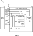
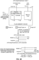
- an exemplary processing system 100 comprising host device 110 and Flash memory device (e.g., UFS memory system) 130, with an interface generally designated with the reference numeral 120 shown between host device 110 and Flash memory device 130.
- Flash memory device e.g., UFS memory system
- Host device 110 may be any processor, core, SoC, etc., which may be designed according to the JEDEC and MIPI standards to support and access Flash memory stored in Flash memory device 130.
- Host device 110 may include various components which have not been specifically illustrated, but may include, for example, a Unipro, M-PHY, a Reference M-PHY Module Interface (RMMI) interface coupled between the Unipro and M-PHY, etc.
- Host device 110 may also include a Host Controller Interface (HCI) to support sending/receiving commands (e.g., CMD 114), data (e.g., data 112), etc., e.g., on interface 120 designed according to the JEDEC standard.
- HCI Host Controller Interface
- Flash memory device 130 Example components are shown for Flash memory device 130 for the sake of elucidation of exemplary aspects, while it will be understood that alternative implementations of Flash memory device 130 are possible without departing from the scope of this disclosure.
- Flash memory device 130 includes an input/output (I/O) block 134, configured to send/receive data, e.g., to/from host device 110, as well as various commands (e.g., associated with read/write functions of the data; CMD 114).
- I/O input/output
- Flash memory device 130 is also shown to comprise memory core 138, which may include one or more banks, arrays, and/or other organization of the memory cells, e.g., designed using Flash memory technology such as NAND Flash memory cells.
- Flash memory device 130 is also shown to include a physical interface (PHY) 135 in communication with controller 136.
- Controller 136 may be a Flash memory controller or UFS controller, generally configured to control access to memory core 138 based, for example, on information from I/O block 134.
- controller 136 may comprise various components such as a central processing unit (CPU) designated as processor 136a, Unipro 136b, etc.
- Power control signals VCC, VCCQ2, VCCQ are shown as part of interface 120, received at Flash memory device 130 from host device 110, which are configured to control corresponding power rails VCC 132a, VCCQ2 132b, VCCQ 132c in Flash memory device 130.
- Power rail VCC 132a which may be at a nominal voltage of 3.3V, for example, may be configured to supply power to memory core 138.
- Power rails VCCQ 132c and VCCQ2 132b may be derived from power rail VCC 132a (e.g., using voltage regulators, not specifically illustrated), which may be at respective nominal voltages of 1.8V and 1.2V, for example, and configured to supply power to I/O block 134, PHY 135, controller 136, etc.
- power and reset control block 133 may be configured to receive an exemplary control signal from host device 110 and/or a hardware reset signal (shown as RESET_N 122, which may be an active-low signal) and turn off the power supply from power rails VCCQ 132c and VCCQ2 132b to the components such as to I/O block 134, PHY 135, controller 136, etc.
- RESET_N 122 which may be an active-low signal
- the control signal and/or hardware reset with reference to exemplary power modes, such as UFS deep power-down modes 1 and 2 will be discussed in further detail in the following sections.
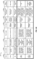
- FIG. 2A In conjunction with FIG. 1 ), some of the power modes which may be available, e.g., according to existing JEDEC standards for UFS memory systems is shown in table 200. Specifically, active mode, idle mode, UFS sleep mode, and UFS power down mode are shown in rows of column 200a, with the characteristics of each of these modes shown in the various columns 200b-h.
- column 200b shows the enter conditions for entering the respective power modes
- column 200c shows the related exit conditions
- column 200d shows the power supply provided in the respective modes
- column 200e shows the link status, e.g., pertaining to data 112 and CMD 114 of interface 120, in the respective modes
- column 200f shows the UFS device status, e.g., of Flash memory device 130 in the respective modes
- column 200g shows the responsiveness, e.g., of Flash memory device 130 to commands from host device 110 in the respective modes
- column 200h illustrates example values for power consumption in the respective modes.
- this mode may be entered (column 200b) when any operation is started on Flash memory device 130 and exited (column 200c) when the operation is complete.
- Power control signals VCC, VCCQ2, VCCQ are configured to activate or turn on all of the power rails VCC 132a, VCCQ2 132b, VCCQ 132c shown in FIG. 1 in the active mode (column 200d), illustrated with the shading corresponding to legend "power on" for the respective blocks PHY 135, controller 136, and memory core 138 (I/O block 134 is not separately shown in this view but may be similarly turned on as the remaining blocks).
- the link status (column 200e) pertaining to data 112 and CMD 114 of interface 120 in the active mode involves support for stalling or burst operations; and the state of Flash memory device 130 (column 200f) is that of the operation (e.g., entered in column 200b) being performed.
- Flash memory device 130 is expected to be responsive to any command (column 200g) which may be received from host device 110, and so correspondingly, the power consumption (column 200h) is fairly high (shown as being significantly greater than the power consumption in the idle mode, and with higher values of ICC, ICCQ2 in FIG. 2C , which will now be discussed in greater detail below).
- this mode may be entered (column 200b) when Flash memory device 130 completes execution of all pending operations and the idle mode is exited (column 200c) when a new operation is to be started by Flash memory device 130.
- Power control signals VCC, VCCQ2, VCCQ are configured to turn on or activate all of the power rails VCC 132a, VCCQ2 132b, VCCQ 132c shown in FIG. 1 in the idle mode (column 200d) as well, similar to the active mode.
- the link status (column 200e) of interface 120 in the idle mode involves support for stalling or hibernating; and the state of Flash memory device 130 (column 200f) is that of being ready to perform any operation (e.g., upon exiting the idle mode in column 200c).
- Flash memory device 130 is expected to be responsive to any command (column 200g) which may be received from host device 110, and so correspondingly, the power consumption (column 200h), while relatively low in comparison to the active mode (since no operation is performed in the idle mode), the power consumption is also relatively high in comparison to the UFS sleep mode, which will now be discussed in greater detail below.
- the UFS sleep mode may be entered (column 200b) when Flash memory device 130 receives a specific command from host device 110, wherein the specific command, in one standard implementation is shown as the START STOP UNIT command with POWER CONDITION set to a value of "2h".
- the UFS sleep mode is exited (column 200c) when the START STOP UNIT command with POWER CONDITION set to a value of "1h" is received from host device 110.
- memory core 138 may be powered down, and so, correspondingly, power control signal VCC is provided to turn off power rail VCC 132a.
- power control signals VCCQ2, VCCQ are provided to activate the power rails VCCQ2 132b and VCCQ 132c as shown in FIG. 2C to supply partial power (shown with shading according to the legend for partial power) to the above-mentioned components such as PHY 135 and controller 136.
- the link status (column 200e) pertaining to data 112 and CMD 114 of interface 120 in the UFS sleep mode involves support for stalling or hibernating; and the state of Flash memory device 130 (column 200f) is in a low power mode, with memory core 138 being powered down as mentioned above.
- Flash memory device 130 is expected to be responsive to at least a subset of commands (column 200g) which may be received from host device 110, e.g., the exit command with POWER CONDITION set to a value of "1h", a REQUEST SENSE command received from host device 110, etc.; while Flash memory device 130 may return an error message to other commands not belonging to the subset of commands to which Flash memory device 130 is expected to remain responsive while in the UFS sleep mode.
- commands column 200g
- the power consumption (column 200h), is also low, corresponding to ICCQ/ICCQ2 in the order of hundreds of uA, since at least memory core 138 (which consumes significant power to remain active) is powered down in the UFS sleep mode.
- the UFS power down mode is yet another low power mode, also shown and described with reference to FIGS. 2A , C.
- the UFS power down mode may be defined in conventional specifications, but as will be understood from the below description, the UFS power down mode may effectively accomplish the same power savings as the UFS sleep mode, even though it has been separately defined with at least some characteristics in columns 200b-h which are different from the respective characteristics of the UFS sleep mode discussed above.
- the UFS power down mode may be entered (column 200b) when Flash memory device 130 receives a specific command from host device 110, wherein the specific command, in one standard implementation is shown as the START STOP UNIT command with POWER CONDITION set to a value of "3h".
- the UFS power down mode is exited (column 200c) when the START STOP UNIT command with POWER CONDITION set to a value of "1h" is received from host device 110 (similar to the UFS sleep mode).
- memory core 138 may be powered down, and so, correspondingly, power control signal VCC is provided to turn off power rail VCC 132a.
- Flash memory device 130 is expected to be responsive to some commands such as the above mentioned exit command (column 200c) received from host device 110.
- power control signals VCCQ2, VCCQ are provided to activate the power rails VCCQ2 132b and VCCQ 132c shown in FIG.
- the link status (column 200e) pertaining to data 112 and CMD 114 of interface 120 in the UFS power down mode may also involve support for stalling or hibernating, similar to the UFS sleep mode; and the state of Flash memory device 130 (column 200f) is in a low power mode, with memory core 138 being powered down as mentioned above.
- Flash memory device 130 is expected to be responsive to at least a subset of commands (column 200g) which may be received from host device 110, e.g., the exit command with POWER CONDITION set to a value of "1h", a REQUEST SENSE command received from host device 110, etc.; while Flash memory device 130 may return an error message to other commands not belonging to the subset of commands to which Flash memory device 130 is expected to remain responsive while in the UFS power down mode.
- commands column 200g
- the power consumption (column 200h), is also low, with corresponding ICCQ/ICCQ2 in the order of hundreds of uA, but effectively the same as or comparable to the power consumption in the UFS sleep mode, since some components such as PHY 135, controller 136, etc., are to remain powered on, at least partially, similar to the UFS sleep mode.
- Flash memory devices 130 may not support an option to turn off the power rails VCCQ2 132b and VCCQ 132c (column 200d) in the UFS power down mode because this may require a dedicated voltage regulator for effecting on/off states of these power rails, and such dedicated voltage regulators may add additional costs. Furthermore, controlling such voltage regulators may also contribute to penalties for exiting and entering the UFS power down mode in columns 200b-c, for example, which may lead to conventional implementations choosing to forego support for the option to turn off the power rails VCCQ2 132b and VCCQ 132c even though the standards may specify that there is an option to do so.
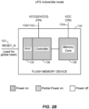
- table 300 is shown, illustrating features of some of the power modes already discussed as being available in existing JEDEC standards for UFS memory systems (e.g., as shown in table 200), juxtaposed with exemplary power modes referred to herein as UFS deep power-down mode 1 and UFS deep power-down mode 2.
- column 300a identifies power modes: UFS sleep and UFS power down (also shown in table 200) and the exemplary power modes UFS deep power-down mode 1 and UFS deep power-down mode 2, with columns 300b-h showing various features of these power modes.
- Flash memory device 130 may be woken up by a hardware reset signal or power cycling. Flash memory device 130 need not be responsive to host device 110 in these modes, which reduces the number of circuits/blocks of Flash memory device 130 which are maintained in powered on (or partially powered on) state in these modes, in turn lowering power consumption to be much smaller than the conventional UFS sleep and UFS power down, e.g., in the order of tens of uA.
- VCCQ2 132b and VCCQ 132c may remain turned on, e.g., by the use of a shared voltage regulator which lowers cost. Such a voltage regulator does not need to be controlled in the UFS deep power-down mode 1 and UFS deep power-down mode 2, which further reduces the enter and exit penalties noted above with respect to conventional low power modes.
- the UFS deep power-down mode 1 may be entered (column 300b) when Flash memory device 130 receives a specific command from host device 110, wherein the specific command, in one exemplary implementation is shown as the START STOP UNIT command with POWER CONDITION set to a value of "4h".
- the UFS deep power-down mode 1 may be exited by the use of options which may not require Flash memory device 130 to be responsive to commands, such as an exit command from host device 110.
- the UFS deep power-down mode 1 may be exited by the use of a hardware reset (active-low) signal being de-asserted, i.e., when it the hardware reset signal transitions from a low to high state.
- a hardware reset active-low
- power cycling to cycle between off and on states may be used to exit the UFS deep power-down mode 1.
- memory core 138 may be powered down, and so, correspondingly, power control signal VCC is provided to turn off power rail VCC 132a.
- Some of the remaining components such as PHY 135, controller 136, etc., remain powered on with corresponding power rails VCCQ2 132b and VCCQ 132c configured to supply partial power (column 300c), but Flash memory device 130 is not expected to be responsive to any commands (e.g., associated with read/write functions of the data; CMD 114) from host device 110, which means that the link, i.e., data 112 and CMD 114 of interface 120 may be powered off, placing Flash memory device 130 in one of the least power consumption states.
- the link e.g., data 112, CMD 114, and/or RESET_N 122
- the link may be a chip-to-chip link.
- the state of Flash memory device 130 may remain in the minimum power mode, with only the reset signal de-assertion or power cycling capable of waking up or placing Flash memory device 130 in a higher power mode.
- column 300g reiterates that while in the UFS deep power-down mode 1, Flash memory device 130 does not need to respond to host device 110, except in the instance of a hardware reset.
- the power consumption of Flash memory device 130 is very low, substantially lower than the conventional UFS sleep mode/UFS power down modes discussed with reference to FIGS. 2A-C .
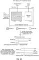
- Table 300 also shows a second exemplary power mode identified as UFS deep power-down mode 2, which will now be discussed in conjunction with an exemplary circuit diagram of FIG. 3C .
- the UFS deep power-down mode 2 may be similar in some aspects to the above-described UFS deep power-down mode 1, with one significant difference being in how these two modes are entered into by Flash memory device 130.
- Flash memory device 130 may enter the UFS deep power-down mode 2 when the above-mentioned hardware reset signal (active-low) being asserted, i.e., transitioned from high to low (rather than in response to a command from host device 110 such as the START STOP UNIT command with POWER CONDITION set to a value of "4h" in the case of UFS deep power-down mode 1 discussed above).
- active-low hardware reset signal
- the UFS deep power-down mode 2 may also be exited by the use of options which may not require Flash memory device 130 to be responsive to commands, such as an exit command from host device 110.
- the UFS deep power-down mode 2 may also be exited by the use of the hardware reset (active-low) signal being de-asserted, i.e., when the hardware reset signal transitions from a low to high state.
- power cycling e.g., effected by host device 110
- memory core 138 may be powered down, and so, correspondingly, power control signal VCC is provided to turn off power rail VCC 132a.
- Some of the remaining components such as PHY 135, controller 136, etc., remain powered on in the UFS deep power-down mode 2 with corresponding power rails VCCQ2 132b and VCCQ 132c configured to supply partial power (column 300c), but Flash memory device 130 is not expected to be responsive to any commands from host device 110, which means that the link, i.e., data 112 and CMD 114 of interface 120 may be powered off, placing Flash memory device 130 in one of the least power consumption states, similar to the UFS deep power-down mode 1.
- the state of Flash memory device 130 may remain in the minimum power mode, with only the reset signal de-assertion or power cycling capable of waking up or placing Flash memory device 130 in a higher power mode.
- column 300g reiterates that while in the UFS deep power-down mode 2, Flash memory device 130 does not need to respond to host device 110, except in the instance of a hardware reset.
- the power consumption of Flash memory device 130 is also very low in the UFS deep power-down mode 2, once again substantially lower than the conventional UFS sleep mode/UFS power down modes discussed with reference to FIGS. 2A-C .
- Column 300e illustrates the link status pertaining to data 112 and CMD 114 of interface 120 in the various above described mode.
- the link status is to stall or hibernate, similar to the link status in these modes discussed with reference to column 200e of FIG. 2A .
- the link status in column 300e shows that interface 120 is powered down or unpowered, which leads to further power savings in these modes since interface 120 is not kept active because Flash memory device 130 is only woken up by a hardware reset or power cycling and is not responsive to commands/data on interface 120 from host device 110.
- FIG. 4 illustrates an exemplary method 400 of power management of a Universal Flash Storage (UFS) memory device (e.g., Flash memory device 130) communicatively coupled to a host device (e.g., host device 110).
- UFS Universal Flash Storage
- FIG. 4 illustrates an exemplary method 400 of power management of a Universal Flash Storage (UFS) memory device (e.g., Flash memory device 130) communicatively coupled to a host device (e.g., host device 110).
- UFS Universal Flash Storage
- Block 402 comprises placing the UFS memory device in at least one low power mode (e.g., deep power-down mode 1 or deep power-down mode 2).
- at least one low power mode e.g., deep power-down mode 1 or deep power-down mode 2.
- Block 404 comprises, while in at least one low power mode (e.g., deep power-down mode 1 or deep power-down mode 2), not responding to any commands which may be received from the host device, thereby enabling a power down state of components which may be needed to be retained in the powered on state if they were required to be responsive to the commands from the host device.
- at least one low power mode e.g., deep power-down mode 1 or deep power-down mode 2
- UFS Universal Flash Storage
- Flash memory device 130 communicatively coupled to a host device (e.g., host device 110) and means for placing the UFS memory device in at least one low power mode (e.g., a command received from host device 110 or RESET_N 122) wherein the UFS memory device is not responsive to any commands received from the host device.
- a host device e.g., host device 110
- RESET_N 122 e.g., a command received from host device 110 or RESET_N 122
- a software module may reside in RAM memory, flash memory, ROM memory, EPROM memory, EEPROM memory, registers, hard disk, a removable disk, a CD-ROM, or any other form of storage medium known in the art.
- An exemplary storage medium is coupled to the processor such that the processor can read information from, and write information to, the storage medium. In the alternative, the storage medium may be integral to the processor.
- an aspect of the invention can include a computer-readable media embodying a method of power management of a Flash memory device. Accordingly, the invention is not limited to illustrated examples and any means for performing the functionality described herein are included in aspects of the invention.
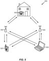
- FIG. 5 illustrates an exemplary wireless communication system 500 in which an aspect of the disclosure may be advantageously employed.
- FIG. 5 shows three remote units 520, 530, and 550 and two base stations 540.
- remote unit 520 is shown as a mobile telephone
- remote unit 530 is shown as a portable computer
- remote unit 550 is shown as a fixed location remote unit in a wireless local loop system.
- the remote units may be a set top box, a music player, a video player, an entertainment unit, a navigation device, a server, a personal digital assistant (PDA), a fixed location data unit, a computer, a laptop, a tablet, a communications device, a mobile phone, or other similar devices that store or retrieve data or computer instructions, or any combination thereof.
- FIG. 5 illustrates remote units according to the teachings of the disclosure, the disclosure is not limited to these exemplary illustrated units. Aspects of the disclosure may be suitably employed in any device which includes active integrated circuitry including memory and on-chip circuitry for test and characterization.
- the foregoing disclosed devices and methods are typically designed and are configured into GDSII and GERBER computer files, stored on a computer-readable media. These files are in turn provided to fabrication handlers who fabricate devices based on these files. The resulting products are semiconductor wafers that are then cut into semiconductor die and packaged into a semiconductor chip. The chips are then employed in devices described above.
- an apparatus comprising: a Universal Flash Storage (UFS) memory device communicatively coupled to a host device, wherein the UFS memory device configured to support one or more power modes, wherein the one or more power modes comprise: at least one low power mode wherein the UFS memory device is not responsive to any commands received from the host device.
- UFS Universal Flash Storage
- the apparatus may further comprise the host device and a link, wherein the host device may provide a command or a hardware reset signal to the UFS memory device via the link.
- the UFS memory device may be configured to enter the at least one low power mode based on:
- the UFS memory device may be configured to exit the at least one low power mode based on:
- the link between the host device and the UFS memory device may be powered down.
- a memory core of the LTFS memory device comprising Flash memory cells may be powered down.
- the memory core may be powered down based on a first power rail configured to supply power to the memory core being turned off.
- one or more of a controller, input/output (I/O) block, or physical interface (PHY) of the UFS memory device may be partially powered on, based on a second power rail and a third power rail being turned on.
- Power consumed by the UFS memory device in the at least one low power mode may be lower than power consumed by the UFS memory device in any other conventional power mode.
- the apparatus may be integrated into a device selected from the group consisting of a set top box, a music player, a video player, an entertainment unit, a navigation device, a server, a personal digital assistant (PDA), a fixed location data unit, a computer, a laptop, a tablet, a communications device, and a mobile phone.
- a device selected from the group consisting of a set top box, a music player, a video player, an entertainment unit, a navigation device, a server, a personal digital assistant (PDA), a fixed location data unit, a computer, a laptop, a tablet, a communications device, and a mobile phone.
- PDA personal digital assistant
- a method of power management of a Universal Flash Storage (UFS) memory device communicatively coupled to a host device comprising: placing the UFS memory device in at least one low power mode wherein the UFS memory device is not responsive to any commands received from the host device.
- UFS Universal Flash Storage
- the method may comprise entering the at least one low power mode based on:
- the method may comprise exiting the at least one low power mode based on:
- the method may comprise, in the at least one low power mode, powering down a link between the host device and the UFS memory device.
- the method may comprise, in the at least one low power mode, powering down a memory core of the UFS memory device comprising Flash memory cells. Powering down the memory core may be based on a first power rail configured to supply power to the memory core being turned on.
- the method may comprise, in the at least one low power mode, partially powering on one or more of a controller, input/output (I/O) block, or physical interface (PHY) of the UFS memory device based on a second power rail and a third power rail being turned on.
- a controller input/output (I/O) block, or physical interface (PHY) of the UFS memory device based on a second power rail and a third power rail being turned on.
- I/O input/output
- PHY physical interface
- Placing the UFS memory device in the at least one low power mode may result in lower power consumed for the UFS memory device than power consumed by the UFS memory device in any other conventional power mode.
- an apparatus comprising: a host device configured to provide a command and a hardware reset signal to a Universal Flash Storage (UFS) memory device, wherein the UFS memory device enters or exits one or more power modes in response to the command or the hardware reset signal, and wherein the UFS memory device in the one or more power modes is not responsive to the command received from the host device.
- a host device configured to provide a command and a hardware reset signal to a Universal Flash Storage (UFS) memory device, wherein the UFS memory device enters or exits one or more power modes in response to the command or the hardware reset signal, and wherein the UFS memory device in the one or more power modes is not responsive to the command received from the host device.
- UFS Universal Flash Storage
- the apparatus may further comprise the UFS memory device and a link, wherein the host device is configured to provide the command and the hardware reset signal via the link.
- the apparatus may be integrated into a device selected from the group consisting of a set top box, a music player, a video player, an entertainment unit, a navigation device, a server, a personal digital assistant (PDA), a fixed location data unit, a computer, a laptop, a tablet, a communications device, and a mobile phone.
- a device selected from the group consisting of a set top box, a music player, a video player, an entertainment unit, a navigation device, a server, a personal digital assistant (PDA), a fixed location data unit, a computer, a laptop, a tablet, a communications device, and a mobile phone.
- PDA personal digital assistant
- an apparatus comprising:
Landscapes
- Engineering & Computer Science (AREA)
- Theoretical Computer Science (AREA)
- Physics & Mathematics (AREA)
- General Engineering & Computer Science (AREA)
- General Physics & Mathematics (AREA)
- Human Computer Interaction (AREA)
- Power Engineering (AREA)
- Techniques For Improving Reliability Of Storages (AREA)
- Read Only Memory (AREA)
- Battery Mounting, Suspending (AREA)
- Memory System Of A Hierarchy Structure (AREA)
- Power Sources (AREA)
Claims (13)
- Eine UFS-Speichereinrichtung (UFS = Universal Flash Storage) (130):
wobei die UFS-Speichereinrichtung konfiguriert ist zum Unterstützen von zwei oder mehr Leistungsmodi, wobei die zwei oder mehr Leistungsmodi Folgendes aufweisen:einen ersten Modus mit niedriger Leistung, in den mit einem Befehl von einer Host-Einrichtung (110) eingetreten wird, die kommunikativ an die UFS-Speichereinrichtung (130) gekoppelt ist,wobei die UFS-Speichereinrichtung in dem ersten Modus mit niedriger Leistung konfiguriert ist auf wenigstens einen Subsatz von Befehlen anzusprechen, der von der Host-Einrichtung empfangen wird;einen zweiten Modus mit niedriger Leistung, wobei die UFS-Speichereinrichtung in dem zweiten Leistungsmodus mit niedriger Leistung konfiguriert ist nicht auf jegliche Befehle anzusprechen, die von der Host-Einrichtung empfangen werden,wobei die UFS-Speichereinrichtung konfiguriert ist in den ersten Modus mit niedriger Leistung einzutreten ansprechend auf den Befehl mit einer ersten Leistungsbedingung und in den zweiten Modus mit niedriger Leistung einzutreten ansprechend auf den Befehl mit einer zweiten Leistungsbedingung, undwobei die UFS-Speichereinrichtung konfiguriert ist aus dem zweiten Modus mit niedriger Leistung auszutreten basierend auf einem Leistungszyklus oder einem Hardware-Reset- bzw. Hardware-Zurücksetzungs-Signal. - UFS-Speichereinrichtung nach Anspruch 1, wobei, in dem zweiten Modus mit niedriger Leistung, ein Speicherkern (138) der UFS-Speichereinrichtung, die Flash-Speicherzellen aufweist, abgeschaltet wird.
- UFS-Speichereinrichtung nach Anspruch 1, wobei, in dem zweiten Modus mit niedriger Leistung, ein oder mehreres von einem Controller (136), einem Eingangs/Ausgangs- bzw. I/O-Block (I = input, O = output) (134) oder eine physische Schnittstelle bzw. PHY (PHY = physical interface) (135) der UFS-Speichereinrichtung partiell angeschaltet wird basierend darauf, dass eine zweite Leistungsschiene (132b) und eine dritte Leistungsschiene (132c) angeschaltet werden.
- UFS-Speichereinrichtung nach Anspruch 1, wobei Leistung, die durch die UFS-Speichereinrichtung in dem zweiten Modus mit niedriger Leistung verbraucht wird, niedriger ist als Leistung, die durch die UFS-Speichereinrichtung in dem Leistungsmodus oder den Leistungsmodi der zwei oder mehr anderen Leistungsmodi als dem zweiten Modus mit niedriger Leistung verbraucht wird.
- UFS-Speichereinrichtung nach Anspruch 1, wobei der Befehl ein START-STOP-UNIT-Befehl ist.
- Eine Vorrichtung, die die UFS-Speichereinrichtung nach Anspruch 1 aufweist, die weiter die Host-Einrichtung (110) und eine Verbindung (120) aufweist, wobei die Host-Einrichtung den Befehl (114) und das Hardware-Reset-Signal (122) an die UFS-Speichereinrichtung über die Verbindung vorsieht.
- Vorrichtung nach Anspruch 6, wobei, in dem zweiten Modus mit niedriger Leistung, die Verbindung zwischen der Host-Einrichtung und der UFS-Speichereinrichtung abgeschaltet wird.
- Eine Host-Einrichtung (110), die konfiguriert ist zum:Vorsehen eines Befehls an eine UFS-Speichereinrichtung (UFS = Universal Flash Storage) (130), die kommunikativ an die Host-Einrichtung (110) gekoppelt ist zum Versetzen der UFS-Speichereinrichtung in einen ersten Modus mit niedriger Leistung, wobei die UFS-Speichereinrichtung in dem ersten Modus mit niedriger Leistung konfiguriert ist auf wenigstens einen Subsatz von Befehlen anzusprechen, der von der Host-Einrichtung empfangen wird;Versetzen der UFS-Speichereinrichtung in einen zweiten Modus mit niedriger Leistung, wobei die UFS-Speichereinrichtung in dem zweiten Modus mit niedriger Leistung konfiguriert ist nicht auf irgendwelche Befehle anzusprechen, die von der Host-Einrichtung empfangen werden und konfiguriert ist aus dem zweiten Modus mit niedriger Leistung auszutreten, und zwar basierend auf einem Leistungszyklus oder einem Hardware-ResetSignal;wobei die Host-Einrichtung konfiguriert ist die UFS-Speichereinrichtung in den ersten Modus mit niedriger Leistung zu versetzen ansprechend auf den Befehl mit einer ersten Leistungsbedingung und in den zweiten Modus mit niedriger Leistung ansprechend auf den Befehl mit einer zweiten Leistungsbedingung.
- Host-Einrichtung nach Anspruch 8, wobei die Host-Einrichtung weiter konfiguriert ist zum Vorsehen des Hardware-Reset-Signals (122).
- Host-Einrichtung nach Anspruch 8, wobei der Befehl ein START-STOP-UNIT-Befehl ist.
- Eine Vorrichtung, die die Host-Einrichtung nach Anspruch 9 aufweist, die weiter die UFS-Speichereinrichtung (130) und eine Verbindung (120) aufweist, wobei die Host-Einrichtung konfiguriert ist zum Vorsehen des Befehls (114) und des Hardware-Reset-Signals (122) über die Verbindung.
- Vorrichtung nach Anspruch 11, wobei, in dem zweiten Modus mit niedriger Leistung, die Verbindung zwischen der Host-Einrichtung und der UFS-Speichereinrichtung abgeschaltet wird.
- Eine UFS-Speichereinrichtung (UFS = Universal Flash Storage) (130):
wobei die UFS-Speichereinrichtung konfiguriert ist zum Unterstützen von zwei oder mehr Leistungsmodi, wobei die zwei oder mehr Leistungsmodi Folgendes aufweisen:einen ersten Modus mit niedriger Leistung, in den mit einem Befehl von einer Host-Einrichtung (110) eingetreten wird, die kommunikativ an die UFS-Speichereinrichtung (130) gekoppelt ist,wobei die UFS-Speichereinrichtung in dem ersten Modus mit niedriger Leistung konfiguriert ist auf wenigstens einen Subsatz von Befehlen anzusprechen, der von der Host-Einrichtung empfangen wird;einen zweiten Modus mit niedriger Leistung, wobei die UFS-Speichereinrichtung in dem zweiten Leistungsmodus mit niedriger Leistung konfiguriert ist nicht auf irgendwelche Befehle anzusprechen, die von der Host-Einrichtung empfangen werden,wobei die UFS-Speichereinrichtung konfiguriert ist in den ersten Modus mit niedriger Leistung einzutreten ansprechend auf den Befehl mit einer ersten Leistungsbedingung und in den zweiten Modus mit niedriger Leistung einzutreten ansprechend auf eine Hardware-Reset-Annahme, undwobei die UFS-Speichereinrichtung konfiguriert ist aus dem zweiten Modus mit niedriger Leistung auszutreten basierend auf einem Leistungszyklus oder einem Hardware-Reset- bzw. Hardware-Zurücksetzungs-Signal.
Applications Claiming Priority (4)
| Application Number | Priority Date | Filing Date | Title |
|---|---|---|---|
| US201762537885P | 2017-07-27 | 2017-07-27 | |
| US16/030,841 US10802736B2 (en) | 2017-07-27 | 2018-07-09 | Power down mode for universal flash storage (UFS) |
| EP18750287.7A EP3659010B1 (de) | 2017-07-27 | 2018-07-11 | Ausschaltmodus für universellen flash-speicher (ufs) |
| PCT/US2018/041628 WO2019022952A1 (en) | 2017-07-27 | 2018-07-11 | STOP MODE FOR UNIVERSAL FLASH MEMORY (UFS) |
Related Parent Applications (2)
| Application Number | Title | Priority Date | Filing Date |
|---|---|---|---|
| EP18750287.7A Division EP3659010B1 (de) | 2017-07-27 | 2018-07-11 | Ausschaltmodus für universellen flash-speicher (ufs) |
| EP18750287.7A Division-Into EP3659010B1 (de) | 2017-07-27 | 2018-07-11 | Ausschaltmodus für universellen flash-speicher (ufs) |
Publications (3)
| Publication Number | Publication Date |
|---|---|
| EP4036689A1 EP4036689A1 (de) | 2022-08-03 |
| EP4036689B1 true EP4036689B1 (de) | 2024-02-21 |
| EP4036689C0 EP4036689C0 (de) | 2024-02-21 |
Family
ID=65040758
Family Applications (2)
| Application Number | Title | Priority Date | Filing Date |
|---|---|---|---|
| EP22163504.8A Active EP4036689B1 (de) | 2017-07-27 | 2018-07-11 | Ausschaltmodus für universellen flash-speicher (ufs) |
| EP18750287.7A Active EP3659010B1 (de) | 2017-07-27 | 2018-07-11 | Ausschaltmodus für universellen flash-speicher (ufs) |
Family Applications After (1)
| Application Number | Title | Priority Date | Filing Date |
|---|---|---|---|
| EP18750287.7A Active EP3659010B1 (de) | 2017-07-27 | 2018-07-11 | Ausschaltmodus für universellen flash-speicher (ufs) |
Country Status (8)
| Country | Link |
|---|---|
| US (2) | US10802736B2 (de) |
| EP (2) | EP4036689B1 (de) |
| CN (2) | CN110945456B (de) |
| BR (1) | BR112020001342A2 (de) |
| ES (1) | ES2974793T3 (de) |
| SG (1) | SG11201911768PA (de) |
| TW (2) | TWI818592B (de) |
| WO (1) | WO2019022952A1 (de) |
Families Citing this family (15)
| Publication number | Priority date | Publication date | Assignee | Title |
|---|---|---|---|---|
| WO2015057556A1 (en) | 2013-10-15 | 2015-04-23 | LIFI Labs, Inc. | Lighting assembly |
| WO2015073890A1 (en) | 2013-11-14 | 2015-05-21 | LIFI Labs, Inc. | Resettable lighting system and method |
| US11455884B2 (en) | 2014-09-02 | 2022-09-27 | LIFI Labs, Inc. | Lighting system |
| US10802736B2 (en) | 2017-07-27 | 2020-10-13 | Qualcomm Incorporated | Power down mode for universal flash storage (UFS) |
| CN111857838B (zh) * | 2019-04-24 | 2024-04-02 | 三星电子株式会社 | 用于管理ufs装置与ufs主机之间的通信的方法和系统 |
| US11113073B2 (en) * | 2019-05-29 | 2021-09-07 | Micron Technology, Inc. | Dual mode hardware reset |
| KR102777357B1 (ko) * | 2019-07-03 | 2025-03-05 | 삼성전자주식회사 | 반도체 시스템 및 반도체 시스템의 동작 방법 |
| US11216058B2 (en) | 2019-07-15 | 2022-01-04 | Micron Technology, Inc. | Storage system deep idle power mode |
| CN113094718A (zh) * | 2019-12-23 | 2021-07-09 | 华为数字技术(苏州)有限公司 | 一种文件加密方法及相关装置 |
| US11314301B2 (en) * | 2020-01-03 | 2022-04-26 | Micron Technolgoy, Inc. | Power management for memory device |
| TWI850537B (zh) | 2021-03-08 | 2024-08-01 | 韓商愛思開海力士有限公司 | 用於一互連協定的功耗模式改變的資訊配置的方法、控制器以及儲存裝置 |
| US11604592B2 (en) * | 2021-06-04 | 2023-03-14 | Western Digital Technologies, Inc. | Data management for efficient low power mode handling in a storage device |
| CN113986001B (zh) * | 2021-10-29 | 2025-02-07 | 深圳市航顺芯片技术研发有限公司 | 芯片及控制方法 |
| CN116667468B (zh) | 2022-02-17 | 2023-12-26 | 荣耀终端有限公司 | 电子设备 |
| CN118228657A (zh) * | 2022-12-19 | 2024-06-21 | 兆易创新科技集团股份有限公司 | 兼具MCU和Flash的系统及其低功耗控制方法 |
Family Cites Families (21)
| Publication number | Priority date | Publication date | Assignee | Title |
|---|---|---|---|---|
| US5822246A (en) * | 1996-09-30 | 1998-10-13 | Intel Corporation | Method and apparatus for detecting the voltage on the VCC pin |
| JP2002318646A (ja) | 2001-04-24 | 2002-10-31 | Sony Corp | 情報処理装置および方法 |
| WO2007043095A1 (ja) * | 2005-09-30 | 2007-04-19 | Spansion Llc | 記憶装置、および記憶装置の制御方法 |
| US7908501B2 (en) * | 2007-03-23 | 2011-03-15 | Silicon Image, Inc. | Progressive power control of a multi-port memory device |
| JP5547154B2 (ja) * | 2011-09-21 | 2014-07-09 | 株式会社東芝 | メモリ・デバイス |
| JP5728370B2 (ja) * | 2011-11-21 | 2015-06-03 | 株式会社東芝 | 半導体記憶装置およびその駆動方法 |
| US8819461B2 (en) * | 2011-12-22 | 2014-08-26 | Intel Corporation | Method, apparatus, and system for energy efficiency and energy conservation including improved processor core deep power down exit latency by using register secondary uninterrupted power supply |
| US9389673B2 (en) * | 2011-12-22 | 2016-07-12 | Sandisk Technologies Inc. | Systems and methods of performing a data save operation |
| US9037890B2 (en) | 2012-07-26 | 2015-05-19 | Artemis Acquisition Llc | Ultra-deep power-down mode for memory devices |
| WO2014141140A1 (en) * | 2013-03-14 | 2014-09-18 | Lsi Corporation | Device power control |
| KR102094902B1 (ko) * | 2013-07-08 | 2020-03-30 | 삼성전자주식회사 | 액티브 상태에서 인터페이스 모드를 전환하는 스토리지 시스템 및 ufs 시스템 |
| KR102108831B1 (ko) * | 2014-01-22 | 2020-05-28 | 삼성전자주식회사 | 저전력을 위해 피지컬 레이어의 웨이크업 신호를 라우트할 수 있는 장치, 이의 동작 방법, 및 상기 장치를 포함하는 데이터 처리 시스템 |
| US8929169B1 (en) * | 2014-05-13 | 2015-01-06 | Sandisk Technologies Inc. | Power management for nonvolatile memory array |
| EP3311384B1 (de) * | 2015-06-19 | 2023-02-08 | Adesto Technologies Corporation | Steuerung von ultratiefem abschaltmodus für eine speichervorrichtung |
| WO2017034852A1 (en) * | 2015-08-21 | 2017-03-02 | Adesto Technologies Corporation | Automatic switch to single spi mode when entering udpd |
| US10331203B2 (en) * | 2015-12-29 | 2019-06-25 | Texas Instruments Incorporated | Compute through power loss hardware approach for processing device having nonvolatile logic memory |
| US9922684B2 (en) | 2016-02-11 | 2018-03-20 | Adesto Technologies Corporation | Memory device ultra-deep power-down mode exit control |
| US10539989B1 (en) | 2016-03-15 | 2020-01-21 | Adesto Technologies Corporation | Memory device alert of completion of internally self-timed power-up and reset operations |
| US10042587B1 (en) * | 2016-03-15 | 2018-08-07 | Adesto Technologies Corporation | Automatic resumption of suspended write operation upon completion of higher priority write operation in a memory device |
| US10235312B2 (en) * | 2016-10-07 | 2019-03-19 | Samsung Electronics Co., Ltd. | Memory system and host device that maintain compatibility with memory devices under previous standards and/or versions of standards |
| US10802736B2 (en) | 2017-07-27 | 2020-10-13 | Qualcomm Incorporated | Power down mode for universal flash storage (UFS) |
-
2018
- 2018-07-09 US US16/030,841 patent/US10802736B2/en active Active
- 2018-07-11 WO PCT/US2018/041628 patent/WO2019022952A1/en not_active Ceased
- 2018-07-11 EP EP22163504.8A patent/EP4036689B1/de active Active
- 2018-07-11 CN CN201880049108.6A patent/CN110945456B/zh active Active
- 2018-07-11 ES ES22163504T patent/ES2974793T3/es active Active
- 2018-07-11 BR BR112020001342-0A patent/BR112020001342A2/pt unknown
- 2018-07-11 SG SG11201911768PA patent/SG11201911768PA/en unknown
- 2018-07-11 CN CN202310815962.1A patent/CN116774807A/zh active Pending
- 2018-07-11 EP EP18750287.7A patent/EP3659010B1/de active Active
- 2018-07-26 TW TW111122583A patent/TWI818592B/zh active
- 2018-07-26 TW TW107125853A patent/TWI771459B/zh active
-
2020
- 2020-09-03 US US17/011,720 patent/US11221774B2/en active Active
Also Published As
| Publication number | Publication date |
|---|---|
| WO2019022952A1 (en) | 2019-01-31 |
| TWI771459B (zh) | 2022-07-21 |
| EP4036689A1 (de) | 2022-08-03 |
| US20190034106A1 (en) | 2019-01-31 |
| EP3659010A1 (de) | 2020-06-03 |
| ES2974793T3 (es) | 2024-07-01 |
| US10802736B2 (en) | 2020-10-13 |
| US20200401333A1 (en) | 2020-12-24 |
| CN110945456A (zh) | 2020-03-31 |
| CN116774807A (zh) | 2023-09-19 |
| EP4036689C0 (de) | 2024-02-21 |
| EP3659010B1 (de) | 2022-04-27 |
| TW201917733A (zh) | 2019-05-01 |
| BR112020001342A2 (pt) | 2020-08-11 |
| TWI818592B (zh) | 2023-10-11 |
| CN110945456B (zh) | 2023-06-20 |
| TW202240588A (zh) | 2022-10-16 |
| SG11201911768PA (en) | 2020-02-27 |
| US11221774B2 (en) | 2022-01-11 |
Similar Documents
| Publication | Publication Date | Title |
|---|---|---|
| EP4036689B1 (de) | Ausschaltmodus für universellen flash-speicher (ufs) | |
| EP3731064B1 (de) | Pmic/pmic-schnittstelle für verteilte speicherverwaltungsimplementierungen | |
| US10892001B2 (en) | Protocol for refresh between a memory controller and a memory device | |
| EP2135249B1 (de) | Progressive leistungssteuerung einer speichervorrichtung mit mehreren anschlüssen | |
| CN106575145B (zh) | 芯片上系统中存储器访问的功率管理 | |
| US9471140B2 (en) | Valid context status retention in processor power mode management | |
| EP3189394B1 (de) | Versorgungsspannungsknotenkopplung unter verwendung eines schalters | |
| US12504806B2 (en) | Mechanism for saving power on a bus interface | |
| US11152046B1 (en) | Sram bit cell retention | |
| US20110138162A1 (en) | Reconfigurable load-reduced memory buffer | |
| US10345885B2 (en) | Power control of a memory device through a sideband channel of a memory bus | |
| US11500446B2 (en) | Reducing power consumption in nonvolatile memory due to standby leakage current | |
| CN111406254A (zh) | 从易失性存储器到非易失性存储器的可配置数据刷新 | |
| HK40022896A (en) | Power down mode for universal flash storage (ufs) | |
| HK40022896B (en) | Power down mode for universal flash storage (ufs) | |
| US7321980B2 (en) | Software power control of circuit modules in a shared and distributed DMA system | |
| US12106818B2 (en) | Power control of a memory device in connected standby state | |
| US20230280809A1 (en) | Method and apparatus to control power supply rails during platform low power events for enhanced usb-c user experience | |
| CN102467225A (zh) | 计算机系统的存储器供电装置及其存储器供电方法 |
Legal Events
| Date | Code | Title | Description |
|---|---|---|---|
| PUAI | Public reference made under article 153(3) epc to a published international application that has entered the european phase |
Free format text: ORIGINAL CODE: 0009012 |
|
| STAA | Information on the status of an ep patent application or granted ep patent |
Free format text: STATUS: REQUEST FOR EXAMINATION WAS MADE |
|
| 17P | Request for examination filed |
Effective date: 20220323 |
|
| AC | Divisional application: reference to earlier application |
Ref document number: 3659010 Country of ref document: EP Kind code of ref document: P |
|
| AK | Designated contracting states |
Kind code of ref document: A1 Designated state(s): AL AT BE BG CH CY CZ DE DK EE ES FI FR GB GR HR HU IE IS IT LI LT LU LV MC MK MT NL NO PL PT RO RS SE SI SK SM TR |
|
| GRAP | Despatch of communication of intention to grant a patent |
Free format text: ORIGINAL CODE: EPIDOSNIGR1 |
|
| STAA | Information on the status of an ep patent application or granted ep patent |
Free format text: STATUS: GRANT OF PATENT IS INTENDED |
|
| RIC1 | Information provided on ipc code assigned before grant |
Ipc: G11C 16/30 20060101ALI20231002BHEP Ipc: G06F 13/16 20060101ALI20231002BHEP Ipc: G11C 5/14 20060101ALI20231002BHEP Ipc: G06F 3/06 20060101ALI20231002BHEP Ipc: G06F 1/3228 20190101ALI20231002BHEP Ipc: G06F 1/3234 20190101AFI20231002BHEP |
|
| INTG | Intention to grant announced |
Effective date: 20231019 |
|
| GRAS | Grant fee paid |
Free format text: ORIGINAL CODE: EPIDOSNIGR3 |
|
| GRAA | (expected) grant |
Free format text: ORIGINAL CODE: 0009210 |
|
| STAA | Information on the status of an ep patent application or granted ep patent |
Free format text: STATUS: THE PATENT HAS BEEN GRANTED |
|
| AC | Divisional application: reference to earlier application |
Ref document number: 3659010 Country of ref document: EP Kind code of ref document: P |
|
| AK | Designated contracting states |
Kind code of ref document: B1 Designated state(s): AL AT BE BG CH CY CZ DE DK EE ES FI FR GB GR HR HU IE IS IT LI LT LU LV MC MK MT NL NO PL PT RO RS SE SI SK SM TR |
|
| REG | Reference to a national code |
Ref country code: GB Ref legal event code: FG4D |
|
| REG | Reference to a national code |
Ref country code: CH Ref legal event code: EP |
|
| REG | Reference to a national code |
Ref country code: DE Ref legal event code: R096 Ref document number: 602018065754 Country of ref document: DE |
|
| REG | Reference to a national code |
Ref country code: IE Ref legal event code: FG4D |
|
| U01 | Request for unitary effect filed |
Effective date: 20240307 |
|
| U07 | Unitary effect registered |
Designated state(s): AT BE BG DE DK EE FI FR IT LT LU LV MT NL PT SE SI Effective date: 20240315 |
|
| REG | Reference to a national code |
Ref country code: GR Ref legal event code: EP Ref document number: 20240400701 Country of ref document: GR Effective date: 20240410 |
|
| PG25 | Lapsed in a contracting state [announced via postgrant information from national office to epo] |
Ref country code: IS Free format text: LAPSE BECAUSE OF FAILURE TO SUBMIT A TRANSLATION OF THE DESCRIPTION OR TO PAY THE FEE WITHIN THE PRESCRIBED TIME-LIMIT Effective date: 20240621 |
|
| REG | Reference to a national code |
Ref country code: ES Ref legal event code: FG2A Ref document number: 2974793 Country of ref document: ES Kind code of ref document: T3 Effective date: 20240701 |
|
| PG25 | Lapsed in a contracting state [announced via postgrant information from national office to epo] |
Ref country code: HR Free format text: LAPSE BECAUSE OF FAILURE TO SUBMIT A TRANSLATION OF THE DESCRIPTION OR TO PAY THE FEE WITHIN THE PRESCRIBED TIME-LIMIT Effective date: 20240221 Ref country code: RS Free format text: LAPSE BECAUSE OF FAILURE TO SUBMIT A TRANSLATION OF THE DESCRIPTION OR TO PAY THE FEE WITHIN THE PRESCRIBED TIME-LIMIT Effective date: 20240521 |
|
| U20 | Renewal fee for the european patent with unitary effect paid |
Year of fee payment: 7 Effective date: 20240614 |
|
| PG25 | Lapsed in a contracting state [announced via postgrant information from national office to epo] |
Ref country code: RS Free format text: LAPSE BECAUSE OF FAILURE TO SUBMIT A TRANSLATION OF THE DESCRIPTION OR TO PAY THE FEE WITHIN THE PRESCRIBED TIME-LIMIT Effective date: 20240521 Ref country code: IS Free format text: LAPSE BECAUSE OF FAILURE TO SUBMIT A TRANSLATION OF THE DESCRIPTION OR TO PAY THE FEE WITHIN THE PRESCRIBED TIME-LIMIT Effective date: 20240621 Ref country code: HR Free format text: LAPSE BECAUSE OF FAILURE TO SUBMIT A TRANSLATION OF THE DESCRIPTION OR TO PAY THE FEE WITHIN THE PRESCRIBED TIME-LIMIT Effective date: 20240221 |
|
| PG25 | Lapsed in a contracting state [announced via postgrant information from national office to epo] |
Ref country code: PL Free format text: LAPSE BECAUSE OF FAILURE TO SUBMIT A TRANSLATION OF THE DESCRIPTION OR TO PAY THE FEE WITHIN THE PRESCRIBED TIME-LIMIT Effective date: 20240221 |
|
| PG25 | Lapsed in a contracting state [announced via postgrant information from national office to epo] |
Ref country code: PL Free format text: LAPSE BECAUSE OF FAILURE TO SUBMIT A TRANSLATION OF THE DESCRIPTION OR TO PAY THE FEE WITHIN THE PRESCRIBED TIME-LIMIT Effective date: 20240221 |
|
| PG25 | Lapsed in a contracting state [announced via postgrant information from national office to epo] |
Ref country code: SM Free format text: LAPSE BECAUSE OF FAILURE TO SUBMIT A TRANSLATION OF THE DESCRIPTION OR TO PAY THE FEE WITHIN THE PRESCRIBED TIME-LIMIT Effective date: 20240221 |
|
| PG25 | Lapsed in a contracting state [announced via postgrant information from national office to epo] |
Ref country code: CZ Free format text: LAPSE BECAUSE OF FAILURE TO SUBMIT A TRANSLATION OF THE DESCRIPTION OR TO PAY THE FEE WITHIN THE PRESCRIBED TIME-LIMIT Effective date: 20240221 |
|
| PG25 | Lapsed in a contracting state [announced via postgrant information from national office to epo] |
Ref country code: SK Free format text: LAPSE BECAUSE OF FAILURE TO SUBMIT A TRANSLATION OF THE DESCRIPTION OR TO PAY THE FEE WITHIN THE PRESCRIBED TIME-LIMIT Effective date: 20240221 |
|
| PG25 | Lapsed in a contracting state [announced via postgrant information from national office to epo] |
Ref country code: SM Free format text: LAPSE BECAUSE OF FAILURE TO SUBMIT A TRANSLATION OF THE DESCRIPTION OR TO PAY THE FEE WITHIN THE PRESCRIBED TIME-LIMIT Effective date: 20240221 Ref country code: SK Free format text: LAPSE BECAUSE OF FAILURE TO SUBMIT A TRANSLATION OF THE DESCRIPTION OR TO PAY THE FEE WITHIN THE PRESCRIBED TIME-LIMIT Effective date: 20240221 Ref country code: RO Free format text: LAPSE BECAUSE OF FAILURE TO SUBMIT A TRANSLATION OF THE DESCRIPTION OR TO PAY THE FEE WITHIN THE PRESCRIBED TIME-LIMIT Effective date: 20240221 Ref country code: CZ Free format text: LAPSE BECAUSE OF FAILURE TO SUBMIT A TRANSLATION OF THE DESCRIPTION OR TO PAY THE FEE WITHIN THE PRESCRIBED TIME-LIMIT Effective date: 20240221 |
|
| REG | Reference to a national code |
Ref country code: DE Ref legal event code: R097 Ref document number: 602018065754 Country of ref document: DE |
|
| PLBE | No opposition filed within time limit |
Free format text: ORIGINAL CODE: 0009261 |
|
| STAA | Information on the status of an ep patent application or granted ep patent |
Free format text: STATUS: NO OPPOSITION FILED WITHIN TIME LIMIT |
|
| 26N | No opposition filed |
Effective date: 20241122 |
|
| PG25 | Lapsed in a contracting state [announced via postgrant information from national office to epo] |
Ref country code: MC Free format text: LAPSE BECAUSE OF FAILURE TO SUBMIT A TRANSLATION OF THE DESCRIPTION OR TO PAY THE FEE WITHIN THE PRESCRIBED TIME-LIMIT Effective date: 20240221 |
|
| PGFP | Annual fee paid to national office [announced via postgrant information from national office to epo] |
Ref country code: GB Payment date: 20250612 Year of fee payment: 8 |
|
| PGFP | Annual fee paid to national office [announced via postgrant information from national office to epo] |
Ref country code: NO Payment date: 20250626 Year of fee payment: 8 |
|
| PGFP | Annual fee paid to national office [announced via postgrant information from national office to epo] |
Ref country code: GR Payment date: 20250625 Year of fee payment: 8 |
|
| U20 | Renewal fee for the european patent with unitary effect paid |
Year of fee payment: 8 Effective date: 20250617 |
|
| PGFP | Annual fee paid to national office [announced via postgrant information from national office to epo] |
Ref country code: IE Payment date: 20250612 Year of fee payment: 8 |
|
| PGFP | Annual fee paid to national office [announced via postgrant information from national office to epo] |
Ref country code: ES Payment date: 20250814 Year of fee payment: 8 |
|
| PGFP | Annual fee paid to national office [announced via postgrant information from national office to epo] |
Ref country code: CH Payment date: 20250801 Year of fee payment: 8 |
|
| PG25 | Lapsed in a contracting state [announced via postgrant information from national office to epo] |
Ref country code: CY Free format text: LAPSE BECAUSE OF FAILURE TO SUBMIT A TRANSLATION OF THE DESCRIPTION OR TO PAY THE FEE WITHIN THE PRESCRIBED TIME-LIMIT; INVALID AB INITIO Effective date: 20180711 |