EP4033501A1 - Permanent current switch and superconducting device - Google Patents
Permanent current switch and superconducting device Download PDFInfo
- Publication number
- EP4033501A1 EP4033501A1 EP20865338.6A EP20865338A EP4033501A1 EP 4033501 A1 EP4033501 A1 EP 4033501A1 EP 20865338 A EP20865338 A EP 20865338A EP 4033501 A1 EP4033501 A1 EP 4033501A1
- Authority
- EP
- European Patent Office
- Prior art keywords
- current switch
- persistent current
- superconducting wire
- resin material
- heater
- Prior art date
- Legal status (The legal status is an assumption and is not a legal conclusion. Google has not performed a legal analysis and makes no representation as to the accuracy of the status listed.)
- Pending
Links
Images





Classifications
-
- H—ELECTRICITY
- H10—SEMICONDUCTOR DEVICES; ELECTRIC SOLID-STATE DEVICES NOT OTHERWISE PROVIDED FOR
- H10N—ELECTRIC SOLID-STATE DEVICES NOT OTHERWISE PROVIDED FOR
- H10N60/00—Superconducting devices
- H10N60/30—Devices switchable between superconducting and normal states
-
- H—ELECTRICITY
- H01—ELECTRIC ELEMENTS
- H01B—CABLES; CONDUCTORS; INSULATORS; SELECTION OF MATERIALS FOR THEIR CONDUCTIVE, INSULATING OR DIELECTRIC PROPERTIES
- H01B12/00—Superconductive or hyperconductive conductors, cables, or transmission lines
- H01B12/02—Superconductive or hyperconductive conductors, cables, or transmission lines characterised by their form
- H01B12/06—Films or wires on bases or cores
-
- H—ELECTRICITY
- H10—SEMICONDUCTOR DEVICES; ELECTRIC SOLID-STATE DEVICES NOT OTHERWISE PROVIDED FOR
- H10N—ELECTRIC SOLID-STATE DEVICES NOT OTHERWISE PROVIDED FOR
- H10N60/00—Superconducting devices
- H10N60/30—Devices switchable between superconducting and normal states
- H10N60/35—Cryotrons
- H10N60/355—Power cryotrons
-
- H—ELECTRICITY
- H01—ELECTRIC ELEMENTS
- H01B—CABLES; CONDUCTORS; INSULATORS; SELECTION OF MATERIALS FOR THEIR CONDUCTIVE, INSULATING OR DIELECTRIC PROPERTIES
- H01B12/00—Superconductive or hyperconductive conductors, cables, or transmission lines
- H01B12/14—Superconductive or hyperconductive conductors, cables, or transmission lines characterised by the disposition of thermal insulation
-
- H—ELECTRICITY
- H01—ELECTRIC ELEMENTS
- H01F—MAGNETS; INDUCTANCES; TRANSFORMERS; SELECTION OF MATERIALS FOR THEIR MAGNETIC PROPERTIES
- H01F6/00—Superconducting magnets; Superconducting coils
- H01F6/006—Supplying energising or de-energising current; Flux pumps
- H01F6/008—Electric circuit arrangements for energising superconductive electromagnets
Definitions
- the present disclosure relates to a persistent current switch and a superconducting device.
- the present application claims priority based on Japanese Patent Application No. 2019-171841 filed on September 20, 2019 .
- the entire contents described in the Japanese patent application are incorporated herein by reference.
- PTL 1 ( WO 2014/034295 ) and PTL 2 ( Japanese Patent Laying-Open No. 2015-053314 ) describe a persistent current switch.
- a superconducting wire is heated by a heater.
- the superconducting wire in the heated portion is normally conducted (an electric resistance value of the superconducting wire in the heated portion increases).
- PTL 3 Japanese Patent Laying-Open No. 2015-198015 describes a superconducting wire.
- the superconducting wire described in PTL 3 includes a substrate, an intermediate layer formed on the substrate, and a superconducting layer formed on the substrate with the intermediate layer interposed therebetween (hereinafter, the superconducting wire having such a structure may be referred to as a thin film superconducting wire).
- a persistent current switch includes a superconducting wire including a substrate and a superconducting layer disposed on the substrate, and a heater.
- the superconducting wire includes a surface including a first portion and a second portion that are disposed apart from each other along a longitudinal direction of the superconducting wire. The first portion and the second portion face each other.
- the heater is sandwiched between the first portion and the second portion.
- the persistent current switches described in PTL 1 and PTL 2 are not the persistent current switch in which the thin film superconducting wire is used. For this reason, how to improve the heating efficiency of the persistent current switch in which the thin film superconducting wire is used as described in PTL 3 is not clear from the above-described conventional technique.
- an object of the present disclosure is to provide a persistent current switch that is configured using the thin film superconducting wire and has the improved heating efficiency.
- the heating efficiency of the persistent current switch configured using the thin film superconducting wire can be improved.
- a configuration of a persistent current switch (hereinafter, referred to as a "persistent current switch 10") according to a first embodiment will be described below.
- Fig. 1 is a side view illustrating persistent current switch 10.
- persistent current switch 10 includes a superconducting wire 1 and a heater 2.
- Persistent current switch 10 may further include a holding member 3 and a filler 4 (not illustrated in Fig. 1 , see Figs. 3 and 4 ).
- Superconducting wire 1 includes a first face 1a and a second face 1b.
- First face 1a includes a first portion 1aa and a second portion 1ab.
- First portion 1aa and second portion 1ab are disposed apart from each other in the longitudinal direction of superconducting wire 1.
- Superconducting wire 1 is bent such that first portion 1aa and second portion 1ab face each other.
- Superconducting wire 1 includes a first end 1c and a second end 1d. First end 1c and second end 1d are ends of superconducting wire 1 in the longitudinal direction.
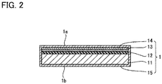
- Fig. 2 is a sectional view orthogonal to the longitudinal direction of superconducting wire 1.
- superconducting wire 1 includes a substrate 11, an intermediate layer 12, and a superconducting layer 13. That is, superconducting wire 1 is a thin film superconducting wire.
- substrate 11 is formed of a clad material in which stainless steel, copper (Cu), and nickel (Ni) are sequentially laminated.
- Intermediate layer 12 is disposed on substrate 11.
- intermediate layer 12 is made of sequentially laminating stabilized zirconia, yttrium oxide, cerium oxide, and the like.
- intermediate layer 12 is formed by a sputtering method.
- Superconducting layer 13 is disposed on substrate 11 with intermediate layer 12 interposed therebetween. Superconducting layer 13 is preferably located closer to first face 1a than substrate 11. Superconducting layer 13 may be located closer to second face 1b than substrate 11.
- superconducting layer 13 is made of an oxide superconductor.
- superconducting layer 13 is formed of REBaCu 3 O y (RE: rare earth element).
- the rare earth element is yttrium (Y), praseodymium (Pr), neodymium (Nd), samarium (Sm), europium (Eu), gadolinium (Gd), holmium (Ho), or ytterbium (Yb).
- superconducting layer 13 is formed by a pulse laser deposition (PLD) method.
- PLD pulse laser deposition
- Superconducting wire 1 further includes a protective layer 14 and a stabilization layer 15.
- Protective layer 14 is disposed on superconducting layer 13.
- Stabilization layer 15 is disposed on protective layer 14.
- Stabilization layer 15 is further disposed on a back surface (a surface opposite to intermediate layer 12) of substrate 11, on the side surface of substrate 11, on the side surface of intermediate layer 12, on the side surface of superconducting layer 13, and on the side surface of protective layer 14.
- protective layer 14 is formed of silver.
- stabilization layer 15 is formed of copper.
- protective layer 14 is formed by a sputtering method, and stabilization layer 15 is formed by an electroplating method.
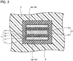
- Fig. 3 is a sectional view taken along a line III-III in Fig. 1 . As illustrated in Figs. 1 and 3 , heater 2 is sandwiched between first portion 1aa and second portion 1ab. From another point of view, both surfaces of heater 2 are in contact with superconducting wire 1.
- Heater 2 includes a heating element 21 and an insulating film 22.
- Heating element 21 is formed of a material that generates Joule heat by energization.
- heating element 21 is made of nichrome.
- Insulating film 22 covers a periphery of heating element 21. This prevents superconducting wire 1 from being short-circuited through heater 2.
- Holding member 3 is a member that prevents deformation of superconducting wire 1 caused by stress due to electromagnetic force applied to superconducting wire 1.
- Holding member 3 is made of a resin material.
- the resin material constituting holding member 3 is referred to as a first resin material.
- Fig. 4 is a sectional view taken along a line IV-IV in Fig. 1 .
- filler 4 is filled between superconducting wire 1 and holding member 3.
- Filler 4 is formed of a resin material.
- the resin material constituting filler 4 is referred to as a second resin material.
- Second resin material is a resin material different from the first resin material.
- the glass transition point of the second resin material (a melting point of the second resin material when the second resin material is a crystalline resin material. the same applies to the following) is less than the glass transition point of the first resin material (a melting point of the first resin material when the first resin material is a crystalline resin material. the same applies to the following).
- the viscosity of the second resin material is preferably lower than the viscosity of the first resin material.
- the viscosity of the first resin material and the viscosity of the second resin material are measured by a method defined in JIS Z 8803: 2011. When the viscosity of the first resin material and the viscosity of the second resin material are compared at the same temperature and when the latter is lower than the former, "the viscosity of the second resin material is lower than the viscosity of the first resin material".
- the second resin material may be a thermoplastic resin material.
- the first resin material are an engineering plastic and a fiber reinforced plastic (FRP).
- FRP fiber reinforced plastic
- a specific example of the second resin material is paraffin.
- the second resin material may be a foamed resin material.
- Persistent current switch 10 is disposed inside a case (not illustrated) and cooled.
- superconducting wire 1 constituting persistent current switch 10 is maintained at a temperature lower than or equal to the superconducting transition temperature.
- this cooling is performed by liquid nitrogen or liquid helium.
- First end 1c and second end 1d are drawn from the case and holding member 3.
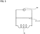
- Fig. 5 is a schematic diagram illustrating the operation of persistent current switch 10. As illustrated in Fig. 5 , superconducting wire 1 (persistent current switch 10) and a superconducting coil 20 are connected in parallel to a power source PW.
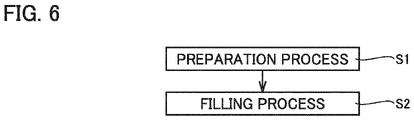
- Fig. 6 is a process diagram illustrating the method for manufacturing persistent current switch 10. As illustrated in Fig. 6 , the method for manufacturing persistent current switch 10 includes a preparation process S1 and a filling process S2.
- Fig. 7 is a sectional view illustrating persistent current switch 10 in preparation process S1. As illustrated in Fig. 7 , in preparation process S1, a void SP remains between holding member 3 and superconducting wire 1.
- filler 4 is filled between superconducting wire 1 and holding member 3 (in void SP).
- firstly holding member 3 and filler 4 are heated.
- the heating temperature at this time is a temperature higher than or equal to the glass transition point of the second resin material and lower than the glass transition point of the first resin material. Filler 4 can easily flow by this heating.
- filler 4 is poured between holding member 3 and superconducting wire 1.
- Filler 4 may be poured between holding member 3 and superconducting wire 1 by immersing holding member 3 in which superconducting wire 1 is held in filler 4 heated to be in the flowing state.
- persistent current switch 30 a persistent current switch
- persistent current switch 40 a persistent current switch
- Fig. 8 is a side view illustrating persistent current switch 30.
- persistent current switch 30 includes superconducting wire 1, heater 2, holding member 3, and filler 4.
- persistent current switch 30 is in common with persistent current switch 10.
- persistent current switch 30 only one surface of heater 2 is in contact with superconducting wire 1. Regarding this point, persistent current switch 30 is different from persistent current switch 10.
- persistent current switch 30 only one portion facing heater 2 in superconducting wire 1 is heated. On the other hand, in persistent current switch 10, two portions facing the heater 2 in superconducting wire 1 are heated. As described above, according to persistent current switch 10, a heating length in superconducting wire 1 is increased, and the resistance of superconducting wire 1 is easily increased.
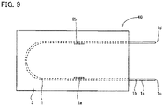
- Fig. 9 is a side view illustrating persistent current switch 40.
- persistent current switch 40 includes superconducting wire 1, heater 2, holding member 3, and filler 4.
- persistent current switch 40 is in common with persistent current switch 10.
- persistent current switch 40 the number of heaters 2 is two (these are referred to as a heater 2a and a heater 2b). In persistent current switch 40, only one surface of heater 2 (heater 2a and heater 2b) is in contact with superconducting wire 1. In these respects, persistent current switch 40 is different from persistent current switch 10.
- persistent current switch 40 two portions facing heater 2a and heater 2b in superconducting wire 1 are heated.
- superconducting wire 1 can be heated at two locations by supplying power to one heater 2, so that the power required to operate heater 2 can be reduced as compared with persistent current switch 40.
- persistent current switch 10 the heating efficiency by heater 2 can be enhanced. That is, persistent current switch 10 enables the operation in the persistent current mode in a short time and with low power.
- Persistent current switch 10 is returned from the cryogenic temperature to the normal temperature.
- the dew condensation is generated on the surface of superconducting wire 1 when persistent current switch 10 is returned from the cryogenic temperature to the normal temperature.
- the dew condensation generated on the surface of superconducting wire 1 causes degradation of a superconducting characteristic of the superconducting wire 1.
- filler 4 When filler 4 is filled between holding member 3 and superconducting wire 1, the surface of superconducting wire 1 is covered with filler 4. Accordingly, even when persistent current switch 10 is returned from the cryogenic temperature to the normal temperature, the dew condensation is hardly generated on the surface of superconducting wire 1.
- holding member 3 When the glass transition point of the second resin material is lower than the glass transition point of the first resin material, holding member 3 is not softened, but filler 4 is softened to be in a flowable state, so that filler 4 is easily filled between holding member 3 and superconducting wire 1.
- Deformation (or dissolution) of holding member 3 can be prevented when the glass transition point of the second resin material is lower than the glass transition point of the first resin material. Furthermore, in this case, when the filling of filler 4 fails, filler 4 can be removed to perform filling process S2 again, so that a yield is improved.
- This filling is more easily performed when the viscosity of the second resin material is lower than the viscosity of the first resin material. In this case, the deformation of holding member 3 can be prevented when filler 4 is filled. In particular, because paraffin has a low melting point, it is easy to handle in filling process S2.
- superconducting wire 1 can be thermally insulated, so that evaporation of the refrigerant can be prevented while the power of heater 2 is reduced.
- a configuration of a persistent current switch (hereinafter, referred to as a "persistent current switch 50") according to a second embodiment will be described below.
- a difference from the configuration of persistent current switch 10 will be mainly described, and redundant description will not be repeated.
- Fig. 10 is a side view illustrating persistent current switch 50.
- persistent current switch 50 includes superconducting wire 1, heater 2, holding member 3, and filler 4.
- the configuration of persistent current switch 50 is common to the configuration of persistent current switch 10.
- Persistent current switch 50 further includes a heater 2c and a heater 2d.
- first face 1a further includes a third portion 1ac, a fourth portion 1ad, a fifth portion 1ae, and a sixth portion 1af.
- First portion 1aa to sixth portion 1af are disposed apart from each other in the longitudinal direction of superconducting wire 1.
- Superconducting wire 1 is bent such that first portion 1aa and second portion 1ab face each other, third portion 1ac and fourth portion 1ad face each other, and fifth portion 1ae and sixth portion 1af face each other.
- Heater 2c is disposed so as to be sandwiched between third portion 1ac and fourth portion 1ad. Heater 2d is disposed so as to be sandwiched between fifth portion 1ae and sixth portion 1af.
- the width of heater 2 in the longitudinal direction of superconducting wire 1 is defined as a width W1
- the width of heater 2c in the longitudinal direction of superconducting wire 1 is defined as a width W2
- the width of heater 2d in the longitudinal direction of superconducting wire 1 is defined as a width W2.
- a distance between heater 2 and heater 2c in the longitudinal direction of superconducting wire 1 is defined as a distance DIS1
- a distance between heater 2c and heater 2d in the longitudinal direction of superconducting wire 1 is defined as a distance DIS2.
- Distance DIS1 is preferably less than or equal to an average value of width W1 and width W2.
- Distance DIS2 is preferably less than or equal to an average value of width W2 and width W3. That is, the distance between the two heaters adjacent to each other in the longitudinal direction of superconducting wire 1 is preferably less than or equal to the average value of the widths of the two heaters adjacent to each other in the longitudinal direction of superconducting wire 1.
- Width W1, width W2, and width W3 may be equal to each other or different from each other.
- Distance DIS1 and distance DIS2 may be equal to each other or different from each other.
- the number of heaters is three, but the number of heaters may be two or at least four.
- Persistent current switch 50 includes a plurality of heaters (heater 2, heater 2c, and heater 2d) disposed apart from each other along the longitudinal direction of superconducting wire 1, and the heaters are in contact with superconducting wire 1 on both surfaces. Consequently, according to persistent current switch 50, superconducting wire 1 is efficiently heated over a long region, so that the resistance of superconducting wire 1 can be efficiently increased over the long region.
- heaters heater 2, heater 2c, and heater 2d
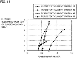
- Fig. 11 is a graph illustrating a relationship between the power supplied to the heater in each of persistent current switch 10, persistent current switch 30, persistent current switch 40, and persistent current switch 50 and the electric resistance value of superconducting wire 1.
- a horizontal axis represents the power (unit: W) supplied to the heater
- a vertical axis represents the electric resistance value (unit: ⁇ ) of superconducting wire 1.
- the heater lengths of persistent current switch 10, persistent current switch 30, and persistent current switch 40 were set to 10 mm.
- width W1 to width W3 were set to 3 mm
- distance DIS1 and distance DIS2 were set to 3 mm.
- the power was equally supplied to each heater.
- the temperatures of persistent current switch 10, persistent current switch 30, persistent current switch 40, and persistent current switch 50 were set to 77 K.
- 1 superconducting wire, 1a: first face, 1aa: first portion, 1ab: second portion, 1ac: third portion, 1ad: fourth portion, 1ae: fifth portion, 1af: sixth portion, 1b: second surface, 1c: first end, 1d: second end, 2, 2a, 2b, 2c, 2d: heater, 3: holding member, 4: filler, 10: persistent current switch, 11: substrate, 12: intermediate layer, 13: superconducting layer, 14: protective layer, 15: stabilization layer, 21: heating element, 22: insulating film, 20: superconducting coil, 30: persistent current switch, 40: persistent current switch, 50: persistent current switch, PW: power source, S1: preparation process, S2: filling process, SP: void
Landscapes
- Containers, Films, And Cooling For Superconductive Devices (AREA)
- Superconductors And Manufacturing Methods Therefor (AREA)
Abstract
Description
- The present disclosure relates to a persistent current switch and a superconducting device. The present application claims priority based on
Japanese Patent Application No. 2019-171841 filed on September 20, 2019 - PTL 1 (
WO 2014/034295 ) and PTL 2 (Japanese Patent Laying-Open No. 2015-053314 PTL 1 andPTL 2, a superconducting wire is heated by a heater. As a result, the superconducting wire in the heated portion is normally conducted (an electric resistance value of the superconducting wire in the heated portion increases). - PTL 3 (
Japanese Patent Laying-Open No. 2015-198015 PTL 3 includes a substrate, an intermediate layer formed on the substrate, and a superconducting layer formed on the substrate with the intermediate layer interposed therebetween (hereinafter, the superconducting wire having such a structure may be referred to as a thin film superconducting wire). -
- PTL 1:
WO 2014/034295 - PTL 2:
Japanese Patent Laying-Open No. 2015-053314 - PTL 3:
Japanese Patent Laying-Open No. 2015-198015 - A persistent current switch according to the present disclosure includes a superconducting wire including a substrate and a superconducting layer disposed on the substrate, and a heater. The superconducting wire includes a surface including a first portion and a second portion that are disposed apart from each other along a longitudinal direction of the superconducting wire. The first portion and the second portion face each other. The heater is sandwiched between the first portion and the second portion.
-
-
Fig. 1 is a side view illustrating a persistentcurrent switch 10. -
Fig. 2 is a sectional view orthogonal to a longitudinal direction of asuperconducting wire 1. -
Fig. 3 is a sectional view taken along a line III-III inFig. 1 . -
Fig. 4 is a sectional view taken along a line IV-IV inFig. 1 . -
Fig. 5 is a schematic diagram illustrating operation of the persistentcurrent switch 10. -
Fig. 6 is a process diagram illustrating a method for manufacturing the persistentcurrent switch 10. -
Fig. 7 is a sectional view illustrating the persistentcurrent switch 10 in a preparation process S1. -
Fig. 8 is a side view illustrating a persistentcurrent switch 30. -
Fig. 9 is a side view illustrating a persistentcurrent switch 40. -
Fig. 10 is a side view illustrating a persistentcurrent switch 50. -
Fig. 11 is a graph illustrating a relationship between power supplied to a heater in each of the persistentcurrent switch 10, the persistentcurrent switch 30, the persistentcurrent switch 40, and the persistentcurrent switch 50 and an electric resistance value of thesuperconducting wire 1. - The persistent current switches described in
PTL 1 andPTL 2 are not the persistent current switch in which the thin film superconducting wire is used. For this reason, how to improve the heating efficiency of the persistent current switch in which the thin film superconducting wire is used as described inPTL 3 is not clear from the above-described conventional technique. - The present disclosure has been made in view of the above-described problems of the prior art. More specifically, an object of the present disclosure is to provide a persistent current switch that is configured using the thin film superconducting wire and has the improved heating efficiency.
- According to the present disclosure, the heating efficiency of the persistent current switch configured using the thin film superconducting wire can be improved.
- First, embodiments of the present disclosure will be listed and described.
- (1) A persistent current switch according to one embodiment includes a superconducting wire having a substrate and a superconducting layer disposed on the substrate, and a heater. The superconducting wire includes a surface including a first portion and a second portion that are disposed apart from each other along a longitudinal direction of the superconducting wire. The first portion and the second portion face each other. The heater is sandwiched between the first portion and the second portion.
According to the persistent current switch of (1), the heating efficiency of the persistent current switch can be improved. - (2) In the persistent current switch of (1), the superconducting layer may be located closer to the surface than the substrate.
According to the persistent current switch of (2), the heating efficiency of the persistent current switch can be further improved. - (3) The persistent current switch of (1) or (2) may further include a holding member and a filler. The superconducting wire may be held inside the holding member. The filler may be filled between the superconducting wire and the holding member. The holding member may be formed of a first resin material. The filler may be formed of a second resin material different from the first resin material.
According to the persistent current switch of (3), dew condensation can be prevented from being generated on a surface of the superconducting wire when the persistent current switch is returned from a cryogenic temperature to a normal temperature. - (4) In the persistent current switch of (3), a glass transition point of the second resin material may be lower than a glass transition point of the first resin material.
According to the persistent current switch of (4), the filler can be easily filled between the holding member and the superconducting wire. - (5) In the persistent current switch of (3) or (4), the first resin material may be a thermosetting resin material. The second resin material may be a thermoplastic resin material.
According to the persistent current switch of (5), the filler can be easily filled between the holding member and the superconducting wire. - (6) In the persistent current switches of (3) to (5), the second resin material may be paraffin or a foamed resin material.
According to the persistent current switch of (6), the superconducting wire can be insulated, so that the heating efficiency can be further improved. - (7) A superconducting device according to another embodiment includes the persistent current switches of (1) to (6) and a superconducting coil connected to the persistent current switch.
- With reference to the drawings, details of embodiments will be described below. In the drawings, the same or corresponding portion is denoted by the same reference numeral, and the description will not be repeated.
- A configuration of a persistent current switch (hereinafter, referred to as a "persistent
current switch 10") according to a first embodiment will be described below. -
Fig. 1 is a side view illustrating persistentcurrent switch 10. As illustrated inFig. 1 , persistentcurrent switch 10 includes asuperconducting wire 1 and aheater 2. Persistentcurrent switch 10 may further include a holdingmember 3 and a filler 4 (not illustrated inFig. 1 , seeFigs. 3 and4 ). -
Superconducting wire 1 includes afirst face 1a and asecond face 1b.First face 1a includes a first portion 1aa and a second portion 1ab. First portion 1aa and second portion 1ab are disposed apart from each other in the longitudinal direction ofsuperconducting wire 1.Superconducting wire 1 is bent such that first portion 1aa and second portion 1ab face each other.Superconducting wire 1 includes afirst end 1c and asecond end 1d.First end 1c andsecond end 1d are ends ofsuperconducting wire 1 in the longitudinal direction. -
Fig. 2 is a sectional view orthogonal to the longitudinal direction ofsuperconducting wire 1. As illustrated inFig. 2 ,superconducting wire 1 includes asubstrate 11, anintermediate layer 12, and asuperconducting layer 13. That is,superconducting wire 1 is a thin film superconducting wire. - For example,
substrate 11 is formed of a clad material in which stainless steel, copper (Cu), and nickel (Ni) are sequentially laminated. -
Intermediate layer 12 is disposed onsubstrate 11. For example,intermediate layer 12 is made of sequentially laminating stabilized zirconia, yttrium oxide, cerium oxide, and the like. For example,intermediate layer 12 is formed by a sputtering method. -
Superconducting layer 13 is disposed onsubstrate 11 withintermediate layer 12 interposed therebetween.Superconducting layer 13 is preferably located closer tofirst face 1a thansubstrate 11.Superconducting layer 13 may be located closer tosecond face 1b thansubstrate 11. - For example,
superconducting layer 13 is made of an oxide superconductor. For example,superconducting layer 13 is formed of REBaCu3Oy (RE: rare earth element). For example, the rare earth element is yttrium (Y), praseodymium (Pr), neodymium (Nd), samarium (Sm), europium (Eu), gadolinium (Gd), holmium (Ho), or ytterbium (Yb). For example,superconducting layer 13 is formed by a pulse laser deposition (PLD) method. -
Superconducting wire 1 further includes aprotective layer 14 and astabilization layer 15.Protective layer 14 is disposed onsuperconducting layer 13.Stabilization layer 15 is disposed onprotective layer 14.Stabilization layer 15 is further disposed on a back surface (a surface opposite to intermediate layer 12) ofsubstrate 11, on the side surface ofsubstrate 11, on the side surface ofintermediate layer 12, on the side surface ofsuperconducting layer 13, and on the side surface ofprotective layer 14. For example,protective layer 14 is formed of silver. For example,stabilization layer 15 is formed of copper. For example,protective layer 14 is formed by a sputtering method, andstabilization layer 15 is formed by an electroplating method. -
Fig. 3 is a sectional view taken along a line III-III inFig. 1 . As illustrated inFigs. 1 and3 ,heater 2 is sandwiched between first portion 1aa and second portion 1ab. From another point of view, both surfaces ofheater 2 are in contact withsuperconducting wire 1. -
Heater 2 includes aheating element 21 and an insulatingfilm 22.Heating element 21 is formed of a material that generates Joule heat by energization. For example,heating element 21 is made of nichrome. Insulatingfilm 22 covers a periphery ofheating element 21. This preventssuperconducting wire 1 from being short-circuited throughheater 2. - As illustrated in
Fig. 1 ,superconducting wire 1 andheater 2 are held inside holdingmember 3. Holdingmember 3 is a member that prevents deformation ofsuperconducting wire 1 caused by stress due to electromagnetic force applied tosuperconducting wire 1. Holdingmember 3 is made of a resin material. Hereinafter, the resin materialconstituting holding member 3 is referred to as a first resin material. -
Fig. 4 is a sectional view taken along a line IV-IV inFig. 1 . As illustrated inFigs. 3 and4 ,filler 4 is filled betweensuperconducting wire 1 and holdingmember 3.Filler 4 is formed of a resin material. Hereinafter, the resinmaterial constituting filler 4 is referred to as a second resin material. Second resin material is a resin material different from the first resin material. - Preferably the glass transition point of the second resin material (a melting point of the second resin material when the second resin material is a crystalline resin material. the same applies to the following) is less than the glass transition point of the first resin material (a melting point of the first resin material when the first resin material is a crystalline resin material. the same applies to the following).
- The viscosity of the second resin material is preferably lower than the viscosity of the first resin material. The viscosity of the first resin material and the viscosity of the second resin material are measured by a method defined in JIS Z 8803: 2011. When the viscosity of the first resin material and the viscosity of the second resin material are compared at the same temperature and when the latter is lower than the former, "the viscosity of the second resin material is lower than the viscosity of the first resin material".
- When the first resin material is a thermosetting resin material, the second resin material may be a thermoplastic resin material. Specific examples of the first resin material are an engineering plastic and a fiber reinforced plastic (FRP). A specific example of the second resin material is paraffin. The second resin material may be a foamed resin material.
- Persistent
current switch 10 is disposed inside a case (not illustrated) and cooled. Thus,superconducting wire 1 constituting persistentcurrent switch 10 is maintained at a temperature lower than or equal to the superconducting transition temperature. For example, this cooling is performed by liquid nitrogen or liquid helium.First end 1c andsecond end 1d are drawn from the case and holdingmember 3. - Operation of persistent
current switch 10 will be described below. -
Fig. 5 is a schematic diagram illustrating the operation of persistentcurrent switch 10. As illustrated inFig. 5 , superconducting wire 1 (persistent current switch 10) and asuperconducting coil 20 are connected in parallel to a power source PW. - When
heater 2 is in an off state (when the current does not flow through heater 2),superconducting coil 20 has coil impedance, so that the current flows exclusively throughsuperconducting layer 13 insuperconducting wire 1 that becomes the superconducting state. Accordingly,superconducting coil 20 is not excited (this state is referred to as a first state). - When
heater 2 is turned on (when the current flows through heater 2),superconducting layer 13 facingheater 2 becomes the normal conducting state. When the current gradually flows in this state, the current also starts to flow through superconducting coil 20 (this state is referred to as a second state). When a predetermined time elapses after a desired current flows, the current does not flow throughsuperconducting wire 1, but the current flows exclusively through superconducting coil 20 (this state is referred to as a third state). - When
heater 2 is turned off again after being in the third state,superconducting layer 13 facingheater 2 returns to the superconducting state. When the current supplied from power source PW is gradually reduced in this state, a part of the current flowing throughsuperconducting coil 20 flows through superconducting wire 1 (this state is referred to as a fourth state). - When the current supplied from power source PW gradually decreases to 0 ampere, the current flows only through
superconducting wire 1 and superconducting coil 20 (this state is referred to as a fifth state). When the fifth state is reached, even when power source PW is cut off, the current continues to flow throughsuperconducting wire 1 and superconducting coil 20 (persistent current mode). In this way, persistentcurrent switch 10 can operatesuperconducting coil 20 in the persistent current mode. - A method for manufacturing persistent
current switch 10 will be described below. -
Fig. 6 is a process diagram illustrating the method for manufacturing persistentcurrent switch 10. As illustrated inFig. 6 , the method for manufacturing persistentcurrent switch 10 includes a preparation process S1 and a filling process S2. - In preparation process S1, holding
member 3 in whichsuperconducting wire 1 is held is prepared.Fig. 7 is a sectional view illustrating persistentcurrent switch 10 in preparation process S1. As illustrated inFig. 7 , in preparation process S1, a void SP remains between holdingmember 3 andsuperconducting wire 1. - In filling process S2,
filler 4 is filled betweensuperconducting wire 1 and holding member 3 (in void SP). In filling process S2, firstly holdingmember 3 andfiller 4 are heated. The heating temperature at this time is a temperature higher than or equal to the glass transition point of the second resin material and lower than the glass transition point of the first resin material.Filler 4 can easily flow by this heating. In filling process S2, after this heating is performed,filler 4 is poured between holdingmember 3 andsuperconducting wire 1. -
Filler 4 may be poured between holdingmember 3 andsuperconducting wire 1 by immersing holdingmember 3 in whichsuperconducting wire 1 is held infiller 4 heated to be in the flowing state. - When poured
filler 4 is cooled and solidified, a space between holdingmember 3 andsuperconducting wire 1 is filled withfiller 4. As described above, persistentcurrent switch 10 having the structure illustrated inFigs. 1 to 4 is formed. - Hereinafter, a basic effect of persistent
current switch 10 will be described in comparison with a persistent current switch (hereinafter, referred to as a "persistentcurrent switch 30") according to a first comparative example and a persistent current switch (hereinafter, referred to as a "persistentcurrent switch 40") according to a second comparative example. -
Fig. 8 is a side view illustrating persistentcurrent switch 30. As illustrated inFig. 8 , persistentcurrent switch 30 includessuperconducting wire 1,heater 2, holdingmember 3, andfiller 4. In this regard, persistentcurrent switch 30 is in common with persistentcurrent switch 10. - However, in persistent
current switch 30, only one surface ofheater 2 is in contact withsuperconducting wire 1. Regarding this point, persistentcurrent switch 30 is different from persistentcurrent switch 10. - In persistent
current switch 30, only oneportion facing heater 2 insuperconducting wire 1 is heated. On the other hand, in persistentcurrent switch 10, two portions facing theheater 2 insuperconducting wire 1 are heated. As described above, according to persistentcurrent switch 10, a heating length insuperconducting wire 1 is increased, and the resistance ofsuperconducting wire 1 is easily increased. -
Fig. 9 is a side view illustrating persistentcurrent switch 40. As illustrated inFig. 9 , persistentcurrent switch 40 includessuperconducting wire 1,heater 2, holdingmember 3, andfiller 4. In this regard, persistentcurrent switch 40 is in common with persistentcurrent switch 10. - However, in persistent
current switch 40, the number ofheaters 2 is two (these are referred to as aheater 2a and aheater 2b). In persistentcurrent switch 40, only one surface of heater 2 (heater 2a andheater 2b) is in contact withsuperconducting wire 1. In these respects, persistentcurrent switch 40 is different from persistentcurrent switch 10. - In persistent
current switch 40, twoportions facing heater 2a andheater 2b insuperconducting wire 1 are heated. On the other hand, according to persistentcurrent switch 10,superconducting wire 1 can be heated at two locations by supplying power to oneheater 2, so that the power required to operateheater 2 can be reduced as compared with persistentcurrent switch 40. - As described above, according to persistent
current switch 10, the heating efficiency byheater 2 can be enhanced. That is, persistentcurrent switch 10 enables the operation in the persistent current mode in a short time and with low power. - In persistent
current switch 10, when superconductinglayer 13 is located closer tofirst face 1a thansubstrate 11, the distance betweensuperconducting layer 13 andheater 2 is shorter than the case wheresuperconducting layer 13 is located closer tosecond face 1b thansubstrate 11. Accordingly, in this case, the heat is easily transferred fromheater 2 tosuperconducting layer 13, and the heating efficiency byheater 2 can be further enhanced. - In persistent
current switch 10, when superconductinglayer 13 is located closer tofirst face 1a thansubstrate 11, bending stress generated insuperconducting layer 13 in bendingsuperconducting wire 1 is compressive stress. Consequently, in this case,superconducting layer 13 is hardly damaged. - Persistent
current switch 10 is returned from the cryogenic temperature to the normal temperature. When there is the gap between holdingmember 3 andsuperconducting wire 1, the dew condensation is generated on the surface ofsuperconducting wire 1 when persistentcurrent switch 10 is returned from the cryogenic temperature to the normal temperature. The dew condensation generated on the surface ofsuperconducting wire 1 causes degradation of a superconducting characteristic of thesuperconducting wire 1. - When
filler 4 is filled between holdingmember 3 andsuperconducting wire 1, the surface ofsuperconducting wire 1 is covered withfiller 4. Accordingly, even when persistentcurrent switch 10 is returned from the cryogenic temperature to the normal temperature, the dew condensation is hardly generated on the surface ofsuperconducting wire 1. - When the glass transition point of the second resin material is lower than the glass transition point of the first resin material, holding
member 3 is not softened, butfiller 4 is softened to be in a flowable state, so thatfiller 4 is easily filled between holdingmember 3 andsuperconducting wire 1. - Deformation (or dissolution) of holding
member 3 can be prevented when the glass transition point of the second resin material is lower than the glass transition point of the first resin material. Furthermore, in this case, when the filling offiller 4 fails,filler 4 can be removed to perform filling process S2 again, so that a yield is improved. - This filling is more easily performed when the viscosity of the second resin material is lower than the viscosity of the first resin material. In this case, the deformation of holding
member 3 can be prevented whenfiller 4 is filled. In particular, because paraffin has a low melting point, it is easy to handle in filling process S2. - When the second resin material is paraffin or a foamed resin material,
superconducting wire 1 can be thermally insulated, so that evaporation of the refrigerant can be prevented while the power ofheater 2 is reduced. - A configuration of a persistent current switch (hereinafter, referred to as a "persistent
current switch 50") according to a second embodiment will be described below. In this case, a difference from the configuration of persistentcurrent switch 10 will be mainly described, and redundant description will not be repeated. -
Fig. 10 is a side view illustrating persistentcurrent switch 50. As illustrated inFig. 10 , persistentcurrent switch 50 includessuperconducting wire 1,heater 2, holdingmember 3, andfiller 4. In this regard, the configuration of persistentcurrent switch 50 is common to the configuration of persistentcurrent switch 10. - Persistent
current switch 50 further includes aheater 2c and aheater 2d. In persistentcurrent switch 50,first face 1a further includes a third portion 1ac, a fourth portion 1ad, a fifth portion 1ae, and a sixth portion 1af. - First portion 1aa to sixth portion 1af are disposed apart from each other in the longitudinal direction of
superconducting wire 1.Superconducting wire 1 is bent such that first portion 1aa and second portion 1ab face each other, third portion 1ac and fourth portion 1ad face each other, and fifth portion 1ae and sixth portion 1af face each other. -
Heater 2c is disposed so as to be sandwiched between third portion 1ac and fourth portion 1ad.Heater 2d is disposed so as to be sandwiched between fifth portion 1ae and sixth portion 1af. - The width of
heater 2 in the longitudinal direction ofsuperconducting wire 1 is defined as a width W1, the width ofheater 2c in the longitudinal direction ofsuperconducting wire 1 is defined as a width W2, and the width ofheater 2d in the longitudinal direction ofsuperconducting wire 1 is defined as a width W2. A distance betweenheater 2 andheater 2c in the longitudinal direction ofsuperconducting wire 1 is defined as a distance DIS1, and a distance betweenheater 2c andheater 2d in the longitudinal direction ofsuperconducting wire 1 is defined as a distance DIS2. - Distance DIS1 is preferably less than or equal to an average value of width W1 and width W2. Distance DIS2 is preferably less than or equal to an average value of width W2 and width W3. That is, the distance between the two heaters adjacent to each other in the longitudinal direction of
superconducting wire 1 is preferably less than or equal to the average value of the widths of the two heaters adjacent to each other in the longitudinal direction ofsuperconducting wire 1. - Width W1, width W2, and width W3 may be equal to each other or different from each other. Distance DIS1 and distance DIS2 may be equal to each other or different from each other. In the above example, the number of heaters is three, but the number of heaters may be two or at least four.
- The effect of persistent
current switch 50 will be described below. In this case, a difference from the effect of persistentcurrent switch 10 will be mainly described, and redundant description will not be repeated. - Persistent
current switch 50 includes a plurality of heaters (heater 2,heater 2c, andheater 2d) disposed apart from each other along the longitudinal direction ofsuperconducting wire 1, and the heaters are in contact withsuperconducting wire 1 on both surfaces. Consequently, according to persistentcurrent switch 50,superconducting wire 1 is efficiently heated over a long region, so that the resistance ofsuperconducting wire 1 can be efficiently increased over the long region. -
Fig. 11 is a graph illustrating a relationship between the power supplied to the heater in each of persistentcurrent switch 10, persistentcurrent switch 30, persistentcurrent switch 40, and persistentcurrent switch 50 and the electric resistance value ofsuperconducting wire 1. InFig. 11 , a horizontal axis represents the power (unit: W) supplied to the heater, and a vertical axis represents the electric resistance value (unit: Ω) ofsuperconducting wire 1. In the example ofFig. 11 , the heater lengths of persistentcurrent switch 10, persistentcurrent switch 30, and persistentcurrent switch 40 were set to 10 mm. In persistentcurrent switch 50, width W1 to width W3 were set to 3 mm, and distance DIS1 and distance DIS2 were set to 3 mm. Furthermore, with respect to persistentcurrent switch 40 and persistentcurrent switch 50, the power was equally supplied to each heater. The temperatures of persistentcurrent switch 10, persistentcurrent switch 30, persistentcurrent switch 40, and persistentcurrent switch 50 were set to 77 K. - As illustrated in
Fig. 11 , when the electric resistance value ofsuperconducting wire 1 in persistentcurrent switch 10 and the electric resistance value ofsuperconducting wire 1 in persistentcurrent switch 30 are compared in supplying the same electric power to the heater, the electric resistance value ofsuperconducting wire 1 in persistentcurrent switch 10 became larger. More specifically, in persistentcurrent switch 10, because the length ofsuperconducting wire 1 heated by the heater was twice that of persistentcurrent switch 30, the electric resistance value ofsuperconducting wire 1 was about twice that of persistentcurrent switch 30. - When persistent
current switch 10 and persistentcurrent switch 40 were compared with respect to the power of the heater necessary for makingsuperconducting wire 1 had the same electric resistance value, the number ofheaters 2 was one in persistentcurrent switch 10, and the number ofheaters 2 was two in persistentcurrent switch 40. For this reason, the power applied toheater 2 of persistentcurrent switch 10 became about half of the power applied to the heaters (heater 2a andheater 2b) of persistentcurrent switch 40. As described above, it has been experimentally found that the heating efficiency by the heater can be improved by persistentcurrent switch 10. - Comparing persistent
current switch 10 and the persistentcurrent switch 50, when the electric resistance value ofsuperconducting wire 1 was relatively low, the power supplied to the heater of persistentcurrent switch 10 was smaller. However, when the electric resistance value ofsuperconducting wire 1 was relatively high, the power supplied to the heater of persistentcurrent switch 50 became smaller in order to obtain the same electric resistance value. As described above, according to persistentcurrent switch 50, it has been revealed thatsuperconducting wire 1 can be efficiently heated over the long region to efficiently increase the resistance ofsuperconducting wire 1 over the long region. - It should be understood that the first and second embodiments disclosed herein are illustrative in all respects and are not restrictive. The scope of the present invention is defined not by the first and second embodiments but by the claims, and is intended to include meanings equivalent to the claims and all modifications within the scope.
- 1: superconducting wire, 1a: first face, 1aa: first portion, 1ab: second portion, 1ac: third portion, 1ad: fourth portion, 1ae: fifth portion, 1af: sixth portion, 1b: second surface, 1c: first end, 1d: second end, 2, 2a, 2b, 2c, 2d: heater, 3: holding member, 4: filler, 10: persistent current switch, 11: substrate, 12: intermediate layer, 13: superconducting layer, 14: protective layer, 15: stabilization layer, 21: heating element, 22: insulating film, 20: superconducting coil, 30: persistent current switch, 40: persistent current switch, 50: persistent current switch, PW: power source, S1: preparation process, S2: filling process, SP: void
Claims (7)
- A persistent current switch comprising:a superconducting wire that includes a substrate and a superconducting layer disposed on the substrate; anda heater,wherein the superconducting wire includes a surface including a first portion and a second portion that are disposed apart from each other along a longitudinal direction of the superconducting wire,the first portion and the second portion face each other, andthe heater is sandwiched between the first portion and the second portion.
- The persistent current switch according to claim 1, wherein the superconducting layer is located closer to the surface than the substrate.
- The persistent current switch according to claim 1 or 2, further comprising:a holding member; anda filler,wherein the superconducting wire is held inside the holding member,the filler is filled between the superconducting wire and the holding member,the holding member is formed of a first resin material, andthe filler is formed of a second resin material different from the first resin material.
- The persistent current switch according to claim 3, wherein a glass transition point of the second resin material is lower than a glass transition point of the first resin material.
- The persistent current switch according to claim 3 or 4, wherein the first resin material is a thermosetting resin material, and
the second resin material is a thermoplastic resin material. - The persistent current switch according to any one of claims 3 to 5, wherein the second resin material is paraffin or a foamed resin material.
- A superconducting device comprising:the persistent current switch according to any one of claims 1 to 6;a superconducting coil connected to the persistent current switch.
Applications Claiming Priority (2)
| Application Number | Priority Date | Filing Date | Title |
|---|---|---|---|
| JP2019171841 | 2019-09-20 | ||
| PCT/JP2020/032810 WO2021054094A1 (en) | 2019-09-20 | 2020-08-31 | Permanent current switch and superconducting device |
Publications (2)
| Publication Number | Publication Date |
|---|---|
| EP4033501A1 true EP4033501A1 (en) | 2022-07-27 |
| EP4033501A4 EP4033501A4 (en) | 2022-12-28 |
Family
ID=74883007
Family Applications (1)
| Application Number | Title | Priority Date | Filing Date |
|---|---|---|---|
| EP20865338.6A Pending EP4033501A4 (en) | 2019-09-20 | 2020-08-31 | PERMANENT CURRENT SWITCH AND SUPERCONDUCTIVE DEVICE |
Country Status (4)
| Country | Link |
|---|---|
| US (1) | US11980106B2 (en) |
| EP (1) | EP4033501A4 (en) |
| JP (1) | JP7507771B2 (en) |
| WO (1) | WO2021054094A1 (en) |
Family Cites Families (12)
| Publication number | Priority date | Publication date | Assignee | Title |
|---|---|---|---|---|
| JP4081021B2 (en) * | 2004-01-09 | 2008-04-23 | 株式会社東芝 | Superconducting current limiting element |
| KR100819454B1 (en) | 2006-10-10 | 2008-04-04 | 학교법인 한국산업기술대학 | Permanent Current Switch Structure |
| JP5513154B2 (en) * | 2010-02-12 | 2014-06-04 | 昭和電線ケーブルシステム株式会社 | Oxide superconducting wire and manufacturing method of oxide superconducting wire |
| JP2011187524A (en) * | 2010-03-05 | 2011-09-22 | Hitachi Ltd | High-temperature superconducting parallel conductor, high-temperature superconducting coil using the same, and high-temperature superconducting magnet |
| JP6047341B2 (en) | 2012-08-29 | 2016-12-21 | 株式会社日立製作所 | Conductive cooling type permanent current switch and superconducting wire manufacturing method |
| JP2014130793A (en) | 2012-11-30 | 2014-07-10 | Fujikura Ltd | Connection structure of oxide superconductive wire material and its manufacturing method |
| JP2015053314A (en) | 2013-09-05 | 2015-03-19 | 株式会社日立製作所 | PERMANENT CURRENT SWITCH, MANUFACTURING METHOD THEREOF, SUPERCONDUCTING MAGNETIC PRODUCT USING THE SAME, CONNECTION COMPONENT AND DIE |
| JP6307987B2 (en) | 2014-04-01 | 2018-04-11 | 住友電気工業株式会社 | Oxide superconducting thin film wire |
| JP6666274B2 (en) | 2017-01-18 | 2020-03-13 | 株式会社東芝 | High temperature superconducting permanent current switch and high temperature superconducting magnet device |
| JP7040730B2 (en) | 2017-11-28 | 2022-03-23 | 東海旅客鉄道株式会社 | Permanent current switch |
| JP7060412B2 (en) | 2018-03-07 | 2022-04-26 | 古河電気工業株式会社 | Permanent current switch and superconducting magnet device |
| JP7119931B2 (en) | 2018-03-27 | 2022-08-17 | セイコーエプソン株式会社 | liquid ejecting head, liquid ejecting apparatus |
-
2020
- 2020-08-31 WO PCT/JP2020/032810 patent/WO2021054094A1/en not_active Ceased
- 2020-08-31 JP JP2021546580A patent/JP7507771B2/en active Active
- 2020-08-31 US US17/760,788 patent/US11980106B2/en active Active
- 2020-08-31 EP EP20865338.6A patent/EP4033501A4/en active Pending
Also Published As
| Publication number | Publication date |
|---|---|
| US11980106B2 (en) | 2024-05-07 |
| JPWO2021054094A1 (en) | 2021-03-25 |
| WO2021054094A1 (en) | 2021-03-25 |
| JP7507771B2 (en) | 2024-06-28 |
| EP4033501A4 (en) | 2022-12-28 |
| US20220344564A1 (en) | 2022-10-27 |
Similar Documents
| Publication | Publication Date | Title |
|---|---|---|
| KR101374177B1 (en) | Methods of splicing 2g rebco high temperature superconductors using partial micro-melting diffusion pressurized splicing by direct face-to-face contact of high temperature superconducting layers and recovering superconductivity by oxygenation annealing | |
| JP6505565B2 (en) | Connection structure of high temperature superconducting conductor, high temperature superconducting coil and high temperature superconducting coil | |
| JP5118990B2 (en) | Superconducting tape wire and defect repair method | |
| JP2007221013A (en) | Permanent current switch | |
| JP5022279B2 (en) | Oxide superconducting current lead | |
| US11980106B2 (en) | Persistent current switch and superconducting device | |
| US20180358153A1 (en) | Oxide superconducting thin film wire and method for producing the same | |
| JP7040730B2 (en) | Permanent current switch | |
| CN118805319A (en) | Heat transfer device | |
| EP4033552B1 (en) | Superconducting wire holding structure | |
| JP6353334B2 (en) | Superconducting current lead | |
| JP5011181B2 (en) | Oxide superconducting current lead | |
| JP7222622B2 (en) | Superconducting coil and superconducting coil device | |
| KR101535844B1 (en) | METHOD OF SPLICING AND REINFORCING OF SPLICING PART FOR PERSISTENT CURRENT MODE OF 2G ReBCO HIGH TEMPERATURE SUPERCONDUCTORS | |
| JP5789696B1 (en) | Superconducting current lead and method of manufacturing superconducting current lead | |
| JP6314022B2 (en) | Superconducting current lead and method of manufacturing superconducting current lead | |
| JP5037193B2 (en) | Oxide superconducting conductor conducting element | |
| JP6238623B2 (en) | Superconducting current lead | |
| KR102603382B1 (en) | Superconducting wire and superconducting coil | |
| US20220393680A1 (en) | Persistent current switch and superconducting device | |
| JP5037146B2 (en) | Oxide superconductor energization element and manufacturing method thereof | |
| KR100993246B1 (en) | Joining method of high temperature superconducting wire to phase conduction part to reduce resistance of phase conduction part in superconducting system | |
| KR102603380B1 (en) | Superconducting wire and superconducting coil | |
| JP2014179526A (en) | Current lead | |
| JP2025536532A (en) | Superconducting cable with solder channel |
Legal Events
| Date | Code | Title | Description |
|---|---|---|---|
| STAA | Information on the status of an ep patent application or granted ep patent |
Free format text: STATUS: THE INTERNATIONAL PUBLICATION HAS BEEN MADE |
|
| PUAI | Public reference made under article 153(3) epc to a published international application that has entered the european phase |
Free format text: ORIGINAL CODE: 0009012 |
|
| STAA | Information on the status of an ep patent application or granted ep patent |
Free format text: STATUS: REQUEST FOR EXAMINATION WAS MADE |
|
| 17P | Request for examination filed |
Effective date: 20220317 |
|
| AK | Designated contracting states |
Kind code of ref document: A1 Designated state(s): AL AT BE BG CH CY CZ DE DK EE ES FI FR GB GR HR HU IE IS IT LI LT LU LV MC MK MT NL NO PL PT RO RS SE SI SK SM TR |
|
| REG | Reference to a national code |
Ref country code: DE Ref legal event code: R079 Free format text: PREVIOUS MAIN CLASS: H01B0012020000 Ipc: H01L0039200000 |
|
| A4 | Supplementary search report drawn up and despatched |
Effective date: 20221128 |
|
| DAV | Request for validation of the european patent (deleted) | ||
| DAX | Request for extension of the european patent (deleted) | ||
| RIC1 | Information provided on ipc code assigned before grant |
Ipc: H01F 6/00 20060101ALI20221122BHEP Ipc: H01B 12/06 20060101ALI20221122BHEP Ipc: H01L 39/20 20060101AFI20221122BHEP |
|
| STAA | Information on the status of an ep patent application or granted ep patent |
Free format text: STATUS: EXAMINATION IS IN PROGRESS |
|
| 17Q | First examination report despatched |
Effective date: 20250123 |
|
| RAP1 | Party data changed (applicant data changed or rights of an application transferred) |
Owner name: SUMITOMO ELECTRIC INDUSTRIES, LTD. Owner name: RIKEN Owner name: JEOL LTD. |
|
| RAP3 | Party data changed (applicant data changed or rights of an application transferred) |
Owner name: SUMITOMO ELECTRIC INDUSTRIES, LTD. Owner name: RIKEN Owner name: JEOL LTD. |