EP4026692B1 - Touch sensor - Google Patents
Touch sensor Download PDFInfo
- Publication number
- EP4026692B1 EP4026692B1 EP20879372.9A EP20879372A EP4026692B1 EP 4026692 B1 EP4026692 B1 EP 4026692B1 EP 20879372 A EP20879372 A EP 20879372A EP 4026692 B1 EP4026692 B1 EP 4026692B1
- Authority
- EP
- European Patent Office
- Prior art keywords
- laminate
- film substrate
- transparent film
- terminal
- touch sensor
- Prior art date
- Legal status (The legal status is an assumption and is not a legal conclusion. Google has not performed a legal analysis and makes no representation as to the accuracy of the status listed.)
- Active
Links
- 239000000758 substrate Substances 0.000 claims description 93
- 230000001681 protective effect Effects 0.000 claims description 55
- 238000005520 cutting process Methods 0.000 claims description 16
- 230000002787 reinforcement Effects 0.000 claims description 7
- 230000002093 peripheral effect Effects 0.000 claims description 5
- 239000012790 adhesive layer Substances 0.000 claims description 4
- 239000010410 layer Substances 0.000 claims description 4
- 239000000463 material Substances 0.000 description 25
- 238000005336 cracking Methods 0.000 description 16
- 238000000034 method Methods 0.000 description 12
- 229920005989 resin Polymers 0.000 description 11
- 239000011347 resin Substances 0.000 description 11
- XLOMVQKBTHCTTD-UHFFFAOYSA-N Zinc monoxide Chemical compound [Zn]=O XLOMVQKBTHCTTD-UHFFFAOYSA-N 0.000 description 8
- 239000012780 transparent material Substances 0.000 description 5
- 230000000052 comparative effect Effects 0.000 description 4
- 239000011787 zinc oxide Substances 0.000 description 4
- RYGMFSIKBFXOCR-UHFFFAOYSA-N Copper Chemical compound [Cu] RYGMFSIKBFXOCR-UHFFFAOYSA-N 0.000 description 3
- 229920000089 Cyclic olefin copolymer Polymers 0.000 description 3
- 229910052782 aluminium Inorganic materials 0.000 description 3
- XAGFODPZIPBFFR-UHFFFAOYSA-N aluminium Chemical compound [Al] XAGFODPZIPBFFR-UHFFFAOYSA-N 0.000 description 3
- 229910052802 copper Inorganic materials 0.000 description 3
- 239000010949 copper Substances 0.000 description 3
- 238000004519 manufacturing process Methods 0.000 description 3
- BQCADISMDOOEFD-UHFFFAOYSA-N Silver Chemical compound [Ag] BQCADISMDOOEFD-UHFFFAOYSA-N 0.000 description 2
- 239000002313 adhesive film Substances 0.000 description 2
- 239000000956 alloy Substances 0.000 description 2
- 229910045601 alloy Inorganic materials 0.000 description 2
- 239000004020 conductor Substances 0.000 description 2
- 238000001514 detection method Methods 0.000 description 2
- 230000000694 effects Effects 0.000 description 2
- AMGQUBHHOARCQH-UHFFFAOYSA-N indium;oxotin Chemical compound [In].[Sn]=O AMGQUBHHOARCQH-UHFFFAOYSA-N 0.000 description 2
- 239000004973 liquid crystal related substance Substances 0.000 description 2
- 229910052751 metal Inorganic materials 0.000 description 2
- 239000002184 metal Substances 0.000 description 2
- 229910044991 metal oxide Inorganic materials 0.000 description 2
- 150000004706 metal oxides Chemical class 0.000 description 2
- 229920001225 polyester resin Polymers 0.000 description 2
- 229920000139 polyethylene terephthalate Polymers 0.000 description 2
- 239000005020 polyethylene terephthalate Substances 0.000 description 2
- 229910052709 silver Inorganic materials 0.000 description 2
- 239000004332 silver Substances 0.000 description 2
- XOLBLPGZBRYERU-UHFFFAOYSA-N tin dioxide Chemical compound O=[Sn]=O XOLBLPGZBRYERU-UHFFFAOYSA-N 0.000 description 2
- 229910001887 tin oxide Inorganic materials 0.000 description 2
- KPAPHODVWOVUJL-UHFFFAOYSA-N 1-benzofuran;1h-indene Chemical compound C1=CC=C2CC=CC2=C1.C1=CC=C2OC=CC2=C1 KPAPHODVWOVUJL-UHFFFAOYSA-N 0.000 description 1
- 239000004925 Acrylic resin Substances 0.000 description 1
- 229920000178 Acrylic resin Polymers 0.000 description 1
- VYZAMTAEIAYCRO-UHFFFAOYSA-N Chromium Chemical compound [Cr] VYZAMTAEIAYCRO-UHFFFAOYSA-N 0.000 description 1
- ZOKXTWBITQBERF-UHFFFAOYSA-N Molybdenum Chemical compound [Mo] ZOKXTWBITQBERF-UHFFFAOYSA-N 0.000 description 1
- 239000004695 Polyether sulfone Substances 0.000 description 1
- 239000004793 Polystyrene Substances 0.000 description 1
- ZLMJMSJWJFRBEC-UHFFFAOYSA-N Potassium Chemical compound [K] ZLMJMSJWJFRBEC-UHFFFAOYSA-N 0.000 description 1
- XUIMIQQOPSSXEZ-UHFFFAOYSA-N Silicon Chemical compound [Si] XUIMIQQOPSSXEZ-UHFFFAOYSA-N 0.000 description 1
- XBJOBWPPZLJOLG-UHFFFAOYSA-N [O-2].[Mg+2].[O-2].[In+3].[O-2].[Zn+2] Chemical class [O-2].[Mg+2].[O-2].[In+3].[O-2].[Zn+2] XBJOBWPPZLJOLG-UHFFFAOYSA-N 0.000 description 1
- AZWHFTKIBIQKCA-UHFFFAOYSA-N [Sn+2]=O.[O-2].[In+3] Chemical class [Sn+2]=O.[O-2].[In+3] AZWHFTKIBIQKCA-UHFFFAOYSA-N 0.000 description 1
- KKEYTLVFLSCKDE-UHFFFAOYSA-N [Sn+2]=O.[O-2].[Zn+2].[O-2] Chemical class [Sn+2]=O.[O-2].[Zn+2].[O-2] KKEYTLVFLSCKDE-UHFFFAOYSA-N 0.000 description 1
- 229910052787 antimony Inorganic materials 0.000 description 1
- WATWJIUSRGPENY-UHFFFAOYSA-N antimony atom Chemical compound [Sb] WATWJIUSRGPENY-UHFFFAOYSA-N 0.000 description 1
- 230000015572 biosynthetic process Effects 0.000 description 1
- DQXBYHZEEUGOBF-UHFFFAOYSA-N but-3-enoic acid;ethene Chemical class C=C.OC(=O)CC=C DQXBYHZEEUGOBF-UHFFFAOYSA-N 0.000 description 1
- 229910052804 chromium Inorganic materials 0.000 description 1
- 239000011651 chromium Substances 0.000 description 1
- 150000001875 compounds Chemical class 0.000 description 1
- 230000007547 defect Effects 0.000 description 1
- 229920001971 elastomer Polymers 0.000 description 1
- 230000005684 electric field Effects 0.000 description 1
- 238000005538 encapsulation Methods 0.000 description 1
- 239000005038 ethylene vinyl acetate Substances 0.000 description 1
- 239000011521 glass Substances 0.000 description 1
- 229910003437 indium oxide Inorganic materials 0.000 description 1
- PJXISJQVUVHSOJ-UHFFFAOYSA-N indium(iii) oxide Chemical compound [O-2].[O-2].[O-2].[In+3].[In+3] PJXISJQVUVHSOJ-UHFFFAOYSA-N 0.000 description 1
- 238000003754 machining Methods 0.000 description 1
- 229910052750 molybdenum Inorganic materials 0.000 description 1
- 239000011733 molybdenum Substances 0.000 description 1
- 238000000059 patterning Methods 0.000 description 1
- 229920001200 poly(ethylene-vinyl acetate) Polymers 0.000 description 1
- 229920002647 polyamide Polymers 0.000 description 1
- 239000004645 polyester resin Substances 0.000 description 1
- 229920006393 polyether sulfone Polymers 0.000 description 1
- 229920013716 polyethylene resin Polymers 0.000 description 1
- -1 polyethylene terephthalate Polymers 0.000 description 1
- 229920005672 polyolefin resin Polymers 0.000 description 1
- 229920002223 polystyrene Polymers 0.000 description 1
- 229920002635 polyurethane Polymers 0.000 description 1
- 239000004814 polyurethane Substances 0.000 description 1
- 229910052700 potassium Inorganic materials 0.000 description 1
- 239000011591 potassium Substances 0.000 description 1
- 229910052710 silicon Inorganic materials 0.000 description 1
- 239000010703 silicon Substances 0.000 description 1
- 229910052814 silicon oxide Inorganic materials 0.000 description 1
- 239000000126 substance Substances 0.000 description 1
- 229920005992 thermoplastic resin Polymers 0.000 description 1
Images


Classifications
-
- G—PHYSICS
- G06—COMPUTING; CALCULATING OR COUNTING
- G06F—ELECTRIC DIGITAL DATA PROCESSING
- G06F3/00—Input arrangements for transferring data to be processed into a form capable of being handled by the computer; Output arrangements for transferring data from processing unit to output unit, e.g. interface arrangements
- G06F3/01—Input arrangements or combined input and output arrangements for interaction between user and computer
- G06F3/03—Arrangements for converting the position or the displacement of a member into a coded form
- G06F3/041—Digitisers, e.g. for touch screens or touch pads, characterised by the transducing means
- G06F3/0412—Digitisers structurally integrated in a display
-
- G—PHYSICS
- G06—COMPUTING; CALCULATING OR COUNTING
- G06F—ELECTRIC DIGITAL DATA PROCESSING
- G06F3/00—Input arrangements for transferring data to be processed into a form capable of being handled by the computer; Output arrangements for transferring data from processing unit to output unit, e.g. interface arrangements
- G06F3/01—Input arrangements or combined input and output arrangements for interaction between user and computer
- G06F3/03—Arrangements for converting the position or the displacement of a member into a coded form
- G06F3/041—Digitisers, e.g. for touch screens or touch pads, characterised by the transducing means
-
- B—PERFORMING OPERATIONS; TRANSPORTING
- B32—LAYERED PRODUCTS
- B32B—LAYERED PRODUCTS, i.e. PRODUCTS BUILT-UP OF STRATA OF FLAT OR NON-FLAT, e.g. CELLULAR OR HONEYCOMB, FORM
- B32B15/00—Layered products comprising a layer of metal
- B32B15/04—Layered products comprising a layer of metal comprising metal as the main or only constituent of a layer, which is next to another layer of the same or of a different material
- B32B15/08—Layered products comprising a layer of metal comprising metal as the main or only constituent of a layer, which is next to another layer of the same or of a different material of synthetic resin
-
- B—PERFORMING OPERATIONS; TRANSPORTING
- B32—LAYERED PRODUCTS
- B32B—LAYERED PRODUCTS, i.e. PRODUCTS BUILT-UP OF STRATA OF FLAT OR NON-FLAT, e.g. CELLULAR OR HONEYCOMB, FORM
- B32B15/00—Layered products comprising a layer of metal
- B32B15/20—Layered products comprising a layer of metal comprising aluminium or copper
-
- B—PERFORMING OPERATIONS; TRANSPORTING
- B32—LAYERED PRODUCTS
- B32B—LAYERED PRODUCTS, i.e. PRODUCTS BUILT-UP OF STRATA OF FLAT OR NON-FLAT, e.g. CELLULAR OR HONEYCOMB, FORM
- B32B25/00—Layered products comprising a layer of natural or synthetic rubber
-
- B—PERFORMING OPERATIONS; TRANSPORTING
- B32—LAYERED PRODUCTS
- B32B—LAYERED PRODUCTS, i.e. PRODUCTS BUILT-UP OF STRATA OF FLAT OR NON-FLAT, e.g. CELLULAR OR HONEYCOMB, FORM
- B32B25/00—Layered products comprising a layer of natural or synthetic rubber
- B32B25/04—Layered products comprising a layer of natural or synthetic rubber comprising rubber as the main or only constituent of a layer, which is next to another layer of the same or of a different material
- B32B25/08—Layered products comprising a layer of natural or synthetic rubber comprising rubber as the main or only constituent of a layer, which is next to another layer of the same or of a different material of synthetic resin
-
- B—PERFORMING OPERATIONS; TRANSPORTING
- B32—LAYERED PRODUCTS
- B32B—LAYERED PRODUCTS, i.e. PRODUCTS BUILT-UP OF STRATA OF FLAT OR NON-FLAT, e.g. CELLULAR OR HONEYCOMB, FORM
- B32B27/00—Layered products comprising a layer of synthetic resin
- B32B27/06—Layered products comprising a layer of synthetic resin as the main or only constituent of a layer, which is next to another layer of the same or of a different material
- B32B27/08—Layered products comprising a layer of synthetic resin as the main or only constituent of a layer, which is next to another layer of the same or of a different material of synthetic resin
-
- B—PERFORMING OPERATIONS; TRANSPORTING
- B32—LAYERED PRODUCTS
- B32B—LAYERED PRODUCTS, i.e. PRODUCTS BUILT-UP OF STRATA OF FLAT OR NON-FLAT, e.g. CELLULAR OR HONEYCOMB, FORM
- B32B27/00—Layered products comprising a layer of synthetic resin
- B32B27/28—Layered products comprising a layer of synthetic resin comprising synthetic resins not wholly covered by any one of the sub-groups B32B27/30 - B32B27/42
- B32B27/286—Layered products comprising a layer of synthetic resin comprising synthetic resins not wholly covered by any one of the sub-groups B32B27/30 - B32B27/42 comprising polysulphones; polysulfides
-
- B—PERFORMING OPERATIONS; TRANSPORTING
- B32—LAYERED PRODUCTS
- B32B—LAYERED PRODUCTS, i.e. PRODUCTS BUILT-UP OF STRATA OF FLAT OR NON-FLAT, e.g. CELLULAR OR HONEYCOMB, FORM
- B32B27/00—Layered products comprising a layer of synthetic resin
- B32B27/30—Layered products comprising a layer of synthetic resin comprising vinyl (co)polymers; comprising acrylic (co)polymers
- B32B27/302—Layered products comprising a layer of synthetic resin comprising vinyl (co)polymers; comprising acrylic (co)polymers comprising aromatic vinyl (co)polymers, e.g. styrenic (co)polymers
-
- B—PERFORMING OPERATIONS; TRANSPORTING
- B32—LAYERED PRODUCTS
- B32B—LAYERED PRODUCTS, i.e. PRODUCTS BUILT-UP OF STRATA OF FLAT OR NON-FLAT, e.g. CELLULAR OR HONEYCOMB, FORM
- B32B27/00—Layered products comprising a layer of synthetic resin
- B32B27/30—Layered products comprising a layer of synthetic resin comprising vinyl (co)polymers; comprising acrylic (co)polymers
- B32B27/306—Layered products comprising a layer of synthetic resin comprising vinyl (co)polymers; comprising acrylic (co)polymers comprising vinyl acetate or vinyl alcohol (co)polymers
-
- B—PERFORMING OPERATIONS; TRANSPORTING
- B32—LAYERED PRODUCTS
- B32B—LAYERED PRODUCTS, i.e. PRODUCTS BUILT-UP OF STRATA OF FLAT OR NON-FLAT, e.g. CELLULAR OR HONEYCOMB, FORM
- B32B27/00—Layered products comprising a layer of synthetic resin
- B32B27/30—Layered products comprising a layer of synthetic resin comprising vinyl (co)polymers; comprising acrylic (co)polymers
- B32B27/308—Layered products comprising a layer of synthetic resin comprising vinyl (co)polymers; comprising acrylic (co)polymers comprising acrylic (co)polymers
-
- B—PERFORMING OPERATIONS; TRANSPORTING
- B32—LAYERED PRODUCTS
- B32B—LAYERED PRODUCTS, i.e. PRODUCTS BUILT-UP OF STRATA OF FLAT OR NON-FLAT, e.g. CELLULAR OR HONEYCOMB, FORM
- B32B27/00—Layered products comprising a layer of synthetic resin
- B32B27/32—Layered products comprising a layer of synthetic resin comprising polyolefins
- B32B27/322—Layered products comprising a layer of synthetic resin comprising polyolefins comprising halogenated polyolefins, e.g. PTFE
-
- B—PERFORMING OPERATIONS; TRANSPORTING
- B32—LAYERED PRODUCTS
- B32B—LAYERED PRODUCTS, i.e. PRODUCTS BUILT-UP OF STRATA OF FLAT OR NON-FLAT, e.g. CELLULAR OR HONEYCOMB, FORM
- B32B27/00—Layered products comprising a layer of synthetic resin
- B32B27/32—Layered products comprising a layer of synthetic resin comprising polyolefins
- B32B27/325—Layered products comprising a layer of synthetic resin comprising polyolefins comprising polycycloolefins
-
- B—PERFORMING OPERATIONS; TRANSPORTING
- B32—LAYERED PRODUCTS
- B32B—LAYERED PRODUCTS, i.e. PRODUCTS BUILT-UP OF STRATA OF FLAT OR NON-FLAT, e.g. CELLULAR OR HONEYCOMB, FORM
- B32B27/00—Layered products comprising a layer of synthetic resin
- B32B27/36—Layered products comprising a layer of synthetic resin comprising polyesters
-
- B—PERFORMING OPERATIONS; TRANSPORTING
- B32—LAYERED PRODUCTS
- B32B—LAYERED PRODUCTS, i.e. PRODUCTS BUILT-UP OF STRATA OF FLAT OR NON-FLAT, e.g. CELLULAR OR HONEYCOMB, FORM
- B32B3/00—Layered products comprising a layer with external or internal discontinuities or unevennesses, or a layer of non-planar shape; Layered products comprising a layer having particular features of form
- B32B3/10—Layered products comprising a layer with external or internal discontinuities or unevennesses, or a layer of non-planar shape; Layered products comprising a layer having particular features of form characterised by a discontinuous layer, i.e. formed of separate pieces of material
- B32B3/14—Layered products comprising a layer with external or internal discontinuities or unevennesses, or a layer of non-planar shape; Layered products comprising a layer having particular features of form characterised by a discontinuous layer, i.e. formed of separate pieces of material characterised by a face layer formed of separate pieces of material which are juxtaposed side-by-side
-
- B—PERFORMING OPERATIONS; TRANSPORTING
- B32—LAYERED PRODUCTS
- B32B—LAYERED PRODUCTS, i.e. PRODUCTS BUILT-UP OF STRATA OF FLAT OR NON-FLAT, e.g. CELLULAR OR HONEYCOMB, FORM
- B32B7/00—Layered products characterised by the relation between layers; Layered products characterised by the relative orientation of features between layers, or by the relative values of a measurable parameter between layers, i.e. products comprising layers having different physical, chemical or physicochemical properties; Layered products characterised by the interconnection of layers
- B32B7/02—Physical, chemical or physicochemical properties
- B32B7/025—Electric or magnetic properties
-
- B—PERFORMING OPERATIONS; TRANSPORTING
- B32—LAYERED PRODUCTS
- B32B—LAYERED PRODUCTS, i.e. PRODUCTS BUILT-UP OF STRATA OF FLAT OR NON-FLAT, e.g. CELLULAR OR HONEYCOMB, FORM
- B32B7/00—Layered products characterised by the relation between layers; Layered products characterised by the relative orientation of features between layers, or by the relative values of a measurable parameter between layers, i.e. products comprising layers having different physical, chemical or physicochemical properties; Layered products characterised by the interconnection of layers
- B32B7/04—Interconnection of layers
- B32B7/12—Interconnection of layers using interposed adhesives or interposed materials with bonding properties
-
- B—PERFORMING OPERATIONS; TRANSPORTING
- B32—LAYERED PRODUCTS
- B32B—LAYERED PRODUCTS, i.e. PRODUCTS BUILT-UP OF STRATA OF FLAT OR NON-FLAT, e.g. CELLULAR OR HONEYCOMB, FORM
- B32B9/00—Layered products comprising a layer of a particular substance not covered by groups B32B11/00 - B32B29/00
-
- B—PERFORMING OPERATIONS; TRANSPORTING
- B32—LAYERED PRODUCTS
- B32B—LAYERED PRODUCTS, i.e. PRODUCTS BUILT-UP OF STRATA OF FLAT OR NON-FLAT, e.g. CELLULAR OR HONEYCOMB, FORM
- B32B9/00—Layered products comprising a layer of a particular substance not covered by groups B32B11/00 - B32B29/00
- B32B9/04—Layered products comprising a layer of a particular substance not covered by groups B32B11/00 - B32B29/00 comprising such particular substance as the main or only constituent of a layer, which is next to another layer of the same or of a different material
- B32B9/045—Layered products comprising a layer of a particular substance not covered by groups B32B11/00 - B32B29/00 comprising such particular substance as the main or only constituent of a layer, which is next to another layer of the same or of a different material of synthetic resin
-
- G—PHYSICS
- G01—MEASURING; TESTING
- G01D—MEASURING NOT SPECIALLY ADAPTED FOR A SPECIFIC VARIABLE; ARRANGEMENTS FOR MEASURING TWO OR MORE VARIABLES NOT COVERED IN A SINGLE OTHER SUBCLASS; TARIFF METERING APPARATUS; MEASURING OR TESTING NOT OTHERWISE PROVIDED FOR
- G01D5/00—Mechanical means for transferring the output of a sensing member; Means for converting the output of a sensing member to another variable where the form or nature of the sensing member does not constrain the means for converting; Transducers not specially adapted for a specific variable
- G01D5/12—Mechanical means for transferring the output of a sensing member; Means for converting the output of a sensing member to another variable where the form or nature of the sensing member does not constrain the means for converting; Transducers not specially adapted for a specific variable using electric or magnetic means
- G01D5/14—Mechanical means for transferring the output of a sensing member; Means for converting the output of a sensing member to another variable where the form or nature of the sensing member does not constrain the means for converting; Transducers not specially adapted for a specific variable using electric or magnetic means influencing the magnitude of a current or voltage
- G01D5/24—Mechanical means for transferring the output of a sensing member; Means for converting the output of a sensing member to another variable where the form or nature of the sensing member does not constrain the means for converting; Transducers not specially adapted for a specific variable using electric or magnetic means influencing the magnitude of a current or voltage by varying capacitance
-
- G—PHYSICS
- G02—OPTICS
- G02F—OPTICAL DEVICES OR ARRANGEMENTS FOR THE CONTROL OF LIGHT BY MODIFICATION OF THE OPTICAL PROPERTIES OF THE MEDIA OF THE ELEMENTS INVOLVED THEREIN; NON-LINEAR OPTICS; FREQUENCY-CHANGING OF LIGHT; OPTICAL LOGIC ELEMENTS; OPTICAL ANALOGUE/DIGITAL CONVERTERS
- G02F1/00—Devices or arrangements for the control of the intensity, colour, phase, polarisation or direction of light arriving from an independent light source, e.g. switching, gating or modulating; Non-linear optics
- G02F1/01—Devices or arrangements for the control of the intensity, colour, phase, polarisation or direction of light arriving from an independent light source, e.g. switching, gating or modulating; Non-linear optics for the control of the intensity, phase, polarisation or colour
- G02F1/13—Devices or arrangements for the control of the intensity, colour, phase, polarisation or direction of light arriving from an independent light source, e.g. switching, gating or modulating; Non-linear optics for the control of the intensity, phase, polarisation or colour based on liquid crystals, e.g. single liquid crystal display cells
- G02F1/133—Constructional arrangements; Operation of liquid crystal cells; Circuit arrangements
- G02F1/1333—Constructional arrangements; Manufacturing methods
- G02F1/13338—Input devices, e.g. touch panels
-
- G—PHYSICS
- G06—COMPUTING; CALCULATING OR COUNTING
- G06F—ELECTRIC DIGITAL DATA PROCESSING
- G06F3/00—Input arrangements for transferring data to be processed into a form capable of being handled by the computer; Output arrangements for transferring data from processing unit to output unit, e.g. interface arrangements
- G06F3/01—Input arrangements or combined input and output arrangements for interaction between user and computer
- G06F3/03—Arrangements for converting the position or the displacement of a member into a coded form
- G06F3/041—Digitisers, e.g. for touch screens or touch pads, characterised by the transducing means
- G06F3/0416—Control or interface arrangements specially adapted for digitisers
- G06F3/04164—Connections between sensors and controllers, e.g. routing lines between electrodes and connection pads
-
- G—PHYSICS
- G06—COMPUTING; CALCULATING OR COUNTING
- G06F—ELECTRIC DIGITAL DATA PROCESSING
- G06F3/00—Input arrangements for transferring data to be processed into a form capable of being handled by the computer; Output arrangements for transferring data from processing unit to output unit, e.g. interface arrangements
- G06F3/01—Input arrangements or combined input and output arrangements for interaction between user and computer
- G06F3/03—Arrangements for converting the position or the displacement of a member into a coded form
- G06F3/041—Digitisers, e.g. for touch screens or touch pads, characterised by the transducing means
- G06F3/044—Digitisers, e.g. for touch screens or touch pads, characterised by the transducing means by capacitive means
- G06F3/0445—Digitisers, e.g. for touch screens or touch pads, characterised by the transducing means by capacitive means using two or more layers of sensing electrodes, e.g. using two layers of electrodes separated by a dielectric layer
-
- H—ELECTRICITY
- H10—SEMICONDUCTOR DEVICES; ELECTRIC SOLID-STATE DEVICES NOT OTHERWISE PROVIDED FOR
- H10K—ORGANIC ELECTRIC SOLID-STATE DEVICES
- H10K50/00—Organic light-emitting devices
- H10K50/80—Constructional details
- H10K50/84—Passivation; Containers; Encapsulations
-
- H—ELECTRICITY
- H10—SEMICONDUCTOR DEVICES; ELECTRIC SOLID-STATE DEVICES NOT OTHERWISE PROVIDED FOR
- H10K—ORGANIC ELECTRIC SOLID-STATE DEVICES
- H10K59/00—Integrated devices, or assemblies of multiple devices, comprising at least one organic light-emitting element covered by group H10K50/00
- H10K59/40—OLEDs integrated with touch screens
-
- B—PERFORMING OPERATIONS; TRANSPORTING
- B32—LAYERED PRODUCTS
- B32B—LAYERED PRODUCTS, i.e. PRODUCTS BUILT-UP OF STRATA OF FLAT OR NON-FLAT, e.g. CELLULAR OR HONEYCOMB, FORM
- B32B2250/00—Layers arrangement
- B32B2250/24—All layers being polymeric
-
- B—PERFORMING OPERATIONS; TRANSPORTING
- B32—LAYERED PRODUCTS
- B32B—LAYERED PRODUCTS, i.e. PRODUCTS BUILT-UP OF STRATA OF FLAT OR NON-FLAT, e.g. CELLULAR OR HONEYCOMB, FORM
- B32B2307/00—Properties of the layers or laminate
- B32B2307/40—Properties of the layers or laminate having particular optical properties
- B32B2307/412—Transparent
-
- B—PERFORMING OPERATIONS; TRANSPORTING
- B32—LAYERED PRODUCTS
- B32B—LAYERED PRODUCTS, i.e. PRODUCTS BUILT-UP OF STRATA OF FLAT OR NON-FLAT, e.g. CELLULAR OR HONEYCOMB, FORM
- B32B2307/00—Properties of the layers or laminate
- B32B2307/50—Properties of the layers or laminate having particular mechanical properties
- B32B2307/558—Impact strength, toughness
-
- B—PERFORMING OPERATIONS; TRANSPORTING
- B32—LAYERED PRODUCTS
- B32B—LAYERED PRODUCTS, i.e. PRODUCTS BUILT-UP OF STRATA OF FLAT OR NON-FLAT, e.g. CELLULAR OR HONEYCOMB, FORM
- B32B2307/00—Properties of the layers or laminate
- B32B2307/70—Other properties
- B32B2307/724—Permeability to gases, adsorption
- B32B2307/7242—Non-permeable
- B32B2307/7246—Water vapor barrier
-
- B—PERFORMING OPERATIONS; TRANSPORTING
- B32—LAYERED PRODUCTS
- B32B—LAYERED PRODUCTS, i.e. PRODUCTS BUILT-UP OF STRATA OF FLAT OR NON-FLAT, e.g. CELLULAR OR HONEYCOMB, FORM
- B32B2457/00—Electrical equipment
- B32B2457/20—Displays, e.g. liquid crystal displays, plasma displays
- B32B2457/208—Touch screens
-
- B—PERFORMING OPERATIONS; TRANSPORTING
- B32—LAYERED PRODUCTS
- B32B—LAYERED PRODUCTS, i.e. PRODUCTS BUILT-UP OF STRATA OF FLAT OR NON-FLAT, e.g. CELLULAR OR HONEYCOMB, FORM
- B32B27/00—Layered products comprising a layer of synthetic resin
- B32B27/34—Layered products comprising a layer of synthetic resin comprising polyamides
-
- B—PERFORMING OPERATIONS; TRANSPORTING
- B32—LAYERED PRODUCTS
- B32B—LAYERED PRODUCTS, i.e. PRODUCTS BUILT-UP OF STRATA OF FLAT OR NON-FLAT, e.g. CELLULAR OR HONEYCOMB, FORM
- B32B27/00—Layered products comprising a layer of synthetic resin
- B32B27/40—Layered products comprising a layer of synthetic resin comprising polyurethanes
-
- G—PHYSICS
- G06—COMPUTING; CALCULATING OR COUNTING
- G06F—ELECTRIC DIGITAL DATA PROCESSING
- G06F2203/00—Indexing scheme relating to G06F3/00 - G06F3/048
- G06F2203/041—Indexing scheme relating to G06F3/041 - G06F3/045
- G06F2203/04103—Manufacturing, i.e. details related to manufacturing processes specially suited for touch sensitive devices
Definitions
- the present invention relates to a touch sensor that is excellent in cracking resistance.
- Touch sensors are in many cases used as input units for various devices (for example, ticket vending machines, ATM machines, mobile phones, and gaming devices) in which display devices such as organic EL, liquid crystal displays, and plasma displays are mounted, together with the display devices.
- display devices such as organic EL, liquid crystal displays, and plasma displays are mounted, together with the display devices.
- the touch sensors each are disposed on the display surface of the display device, and thus the touch sensor allows for very direct input to the display device.
- US 2017/185187 A1 discloses a conductive film for a touch panel including: a flexible transparent resin substrate having a thickness equal to or smaller than 40 ⁇ m; a plurality of detection electrodes which are formed on at least one surface of the resin substrate; a plurality of peripheral wirings which are formed on at least one surface of the resin substrate and respectively connected to the plurality of detection electrodes; and a plurality of external connection terminals which are formed on at least one surface of the resin substrate and respectively connected to the plurality of peripheral wirings, in which the plurality of external connection terminals are arranged such that adjacent external connection terminals are separated from each other by a distance between terminals of 100 ⁇ m to 200 ⁇ m with a pitch equal to or smaller than 500 ⁇ m, and respectively have a terminal width equal to or greater than the distance between terminals.
- JP 2013 143048 A discloses a conventional touch panel sensor and touch panel sensor having flexible printed wiring board.
- JP 2017 037509 A discloses a conventional wiring body assembly, structure with conductor layer, and touch sensor.
- WO 2018/181175 A1 discloses a conventional wiring body, wiring board, and touch sensor.
- WO 2017/126454 A1 discloses a conventional conductive film laminate.
- CN 208 938 073 U discloses a conventional double-deck encapsulation type touch panel.
- WO 2016/038940 A1 discloses a conventional conductive film for touch panels.
- WO 2015/015691 A1 discloses a conventional touch panel sensor sheet module and a method for manufacturing touch panel system module.
- a touch sensor of some of the touch sensors which is referred to as an electrostatic capacitance method, is configured to form an electric field by applying a weak current to the touch sensor surface and to output, as a signal, a contact position that is obtained by converting a change in capacitance value, when a conductor such as a finger is slightly touched, to a decrease in voltage or the like and detecting the change.
- a touch sensor in which a transparent electrode and a connection terminal section are formed on a pair of opposing substrates is generally known as the touch sensor used in the electrostatic capacitance method. Additionally, a touch sensor in which a transparent electrode and a connection terminal section are formed respectively on both sides of a single transparent substrate (hereinafter, referred as a double-sided touch sensor) is known as another aspect (for example, Patent Document 1).
- the double-sided touch sensor includes a small number of members, which can provide a touch sensor with reduction in thickness, improvement in productivity that is allowed by manufacturing with a roll-to-roll process, or the like. Moreover, since there is no need to bond two substrates together, defects such as positional misalignment between the two transparent electrodes can be avoided.
- the structure of the double-sided touch sensor a structure in which an upper protective film and a lower protective film are bonded together on a transparent film substrate of resin, glass, or the like including surfaces is widely used, where a film including a transparent conductive film being adhered thereon is applied on one of opposing surfaces of the transparent film substrate, on which metal patterning is formed, as the upper protective film and a film including a transparent conductive film being adhered thereon is applied on the other of the opposing surfaces of the transparent film substrate as the lower protective film.
- Electrodes and a control circuit of the touch sensor are connected through a flexible printed circuit board (hereinafter, referred to as FPC).
- FPC flexible printed circuit board
- a wiring board terminal section located at one end portion of the FPC is connected to a front terminal and a back terminal that are located on the transparent film substrate.
- the upper protective film and the lower protective film are provided with a cut portion at the position corresponding to an FPC bonding portion, thereby bonding between the FPC and a sheet terminal section is facilitated.
- the double-sided touch sensor is manufactured through a process of outline blanking for cutting to a predetermined product size.
- a cushion material 18 is provided at an inner side of an outline blanking die 17. Accordingly, at the time of cutting to the predetermined production size with the outline blanking die 17, the upper protective film 2 is pressed against the cushion material 18 at the inner side of the outline blanking die 17, and stress is applied in the vertical direction.
- Patent Document 1 JP 4901660 A
- An object of the present invention is to provide a touch sensor that has solved the problem described above and is excellent in cracking resistance.
- a touch sensor of a first aspect of the present invention is provided as recited in claim 1.
- a touch sensor is provided as recited in claim 2.
- the touch sensor of the first aspect of the invention is provided with a cut portion in a first laminate and the touch sensor of the second aspect of the invention is provided with a cut portion in both a first and second laminate, where the cut portion may be configured such that an upper base of the trapezoidal shape meeting an outer peripheral line 13 forms an outer angle of 30 degrees or more to 60 degrees or less.
- a touch sensor of an aspect of the present invention that is excellent in cracking resistance includes, a transparent film substrate, a front electrode formed on one surface of the transparent film substrate, a front terminal formed on the surface of the transparent film substrate where the front electrode is formed, the front terminal being connected to the front electrode, a back electrode formed on the other surface of the transparent film substrate; and a back terminal formed on the surface of the transparent film substrate where the back electrode is formed, the back terminal being not overlapping with the front terminal in a plan view and being connected to the back electrode.
- the transparent film substrate includes a connection terminal section on an inner side of one side of the transparent film substrate.
- the transparent film substrate is layered with a pair of films of an upper protective film and a lower protective film.
- each of the cut portions is formed to have a trapezoidal shape that gradually widens from an opening end toward an inward portion of the cut portion in a plan view. Accordingly, by forming the cut portion having the trapezoidal shape that widens from the opening end toward the inward portion, stress applied to the transparent film substrate of the cut portion during pressurizing by outline blanking is relieved, and thus cracking is less likely to be generated at the interface portion of the transparent film substrate.
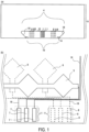
- the touch sensor 9 includes a transparent film substrate 1, a front electrode 5 formed on one surface of the transparent film substrate 1, front terminals 7 formed on the surface of the transparent film substrate 1 where the front electrode 5 is formed, and the front terminals 7 being connected to the front electrode 5, a back electrode 6 formed on the other surface of the transparent film substrate 1, and back terminals 8 formed on the surface of the transparent film substrate 1 where the back electrode 6 is formed, the back terminal 8 being not overlapping with the front terminals 7 in a plan view and being connected to the back electrode 6.
- the transparent film substrate 1 includes connection terminal sections 11 being where the front terminals 7 and back terminals 8 are provided.
- the transparent film substrate 1 is laminated with a pair of films of an upper protective film 2 and a lower protective film 3.
- each of the cut portions 4 is formed to have a trapezoidal shape that gradually widens from an opening end 10 toward an inward portion 12 of the cut portion 4 in a plan view (see FIGS. 1(a) and (b) ).
- the transparent film substrate 1 has a structure that is laminated with the pair of films of the upper protective film 2 and the lower protective film 3, and prevents damage or the like due to external impact. Additionally, the transparent film substrate 1 is laminated with the upper protective film 2 and the lower protective film 3, therefore preventing moisture or the like from entering from the outside.
- each of the upper protective film 2 and the lower protective film 3 is provided with the cut portion 4 that allows the front terminal 7 portion and the back terminals 8 provided on the transparent film substrate 1 to be exposed, which is formed to have a trapezoidal shape that gradually widens from the opening end 10 toward the inward portion 12 of the cut portion 4 in a plan view.
- the material constituting the transparent film substrate 1 are not particularly limited as long as the material is formed of resin having transparency, however, specifically, the examples may include polyethylene resins such as cycloolefin polymer (COP) and polyethylene terephthalate (PET), and a polyester resin such as polyether sulfone.
- the thickness of the transparent film substrate 1 used in an embodiment of the present invention is not particularly limited as long as the thickness can stably support the front electrode 5, the back electrode 6, the front terminals 7, the back terminals 8, the connection terminal sections 11, and the like, however, the thickness can be normally in a range of 50 ⁇ m to 100 ⁇ m.
- the material may be supplied in any form of a roll shape and a wafer shape, and the supplied form may be selected in accordance with the machining method and the processing machine.
- the front electrode 5 according to an embodiment of the present invention is formed on one surface of the transparent film substrate 1, and the back electrode 6 is formed on the other surface of the transparent film substrate 1.
- the examples of the material constituting the front electrode 5 and the back electrode 6 are not particularly limited as long as the material has desired conductivity, and the material may be a transparent material having transparency or a non-transparent material having no transparency, however, the material is preferably a transparent material.
- a material typically applied in the touch sensor 9 can be used as the transparent material in an embodiment of the present invention, and the examples of the material may include metal oxides such as indium tin oxide (ITO), zinc oxide, indium oxide, antimony doped tin oxide, fluorine-doped tin oxide, aluminum doped zinc oxide, potassium doped zinc oxide, and silicon doped zinc oxide or zinc oxide-tin oxide series, indium oxide-tin oxide series, zinc oxide-indium oxide-magnesium oxide series, or a material formed of a compound of two or more types of these metal oxides.
- metal such as aluminum, molybdenum, silver, chromium, or copper, an alloy thereof, or the like can be applied as the non-transparent material.
- the formation pattern, thickness, and the like of the front electrode 5 and the back electrode 6 can be the same as those of a typical touch sensor.
- the front terminals 7 are formed on the surface of the transparent film substrate 1 where the front electrode 5 is formed, and is connected to the front electrode 5.
- the back terminals 8 are formed on the surface of the transparent film substrate 1 where the back electrode 6 is formed, so as not to overlap with the front terminals 7 in a plan view, and the back terminals 8 are connected to the back electrode 6 and are directly formed on the surface of the transparent film substrate 1 (see FIG. 5 ).
- connection terminals 7 and the back terminals 8 easily and efficiently allow for connection of the touch sensor 9 and the FPC in units of the connection terminal sections 11.
- the number or the like of terminals included in the connection terminal section 11 is set as appropriate in accordance with a heat tool or the like used for connecting to the FPC.
- connection terminal section 11 typically includes a plurality of terminals arranged in parallel on the same surface of the transparent film substrate 1 (see FIG. 1(b) ).
- FIG. 2 is (a) plan view and (b) cross-sectional view of the touch sensor 9 according to an embodiment of the present invention. Note that the cross-sectional view of FIG. 2(b) is a cross-sectional view corresponding to a cross-section taken along line A-A in the plan view of FIG. 2(a) .
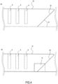
- FIG. 5 is an exploded perspective view of the touch sensor 9 according to an embodiment of the present invention.
- the distance between the front terminal 7 and the back terminal 8 that are located side by side in an embodiment of the present invention is not particularly limited and may be typical distance for the touch sensor 9.
- the material constituting the front terminal 7 and the back terminal 8 according to an embodiment of the present invention is not particularly limited as long as the material can obtain desired conductivity.
- the material can obtain desired conductivity.
- aluminum, silver, copper, an alloy thereof, or the like can be used as the material.
- the terminal width, thickness, and shape in a plan view of the front terminal 7 portion and the back terminal 8 portion, and the distance between the terminals in the connection terminal section 11 can be the same as those in a typical touch sensor.
- the upper protective film 2 and the lower protective film 3 according to an embodiment of the present invention are not particularly limited as long as the upper protective film 2 and the lower protective film 3 have insulating properties, however, in a case where the upper protective film 2 and the lower protective film 3 are formed to cover the electrodes described above, the upper protective film 2 and the lower protective film 3 preferably have transparency.
- the examples of the upper protective film 2 and the lower protective film 3 that have insulating properties and transparency as just described may include an acrylic resin, SiOz, and the like, and thermoplastic resins such as a polyurethane-based resin, a polyester-based resin, a polystyrene-based resin, a polyamide-based resin, a chlorinated polyolefin resin, a chlorinated ethylene-vinyl acetate copolymer resin, a cyclized rubber, and a coumarone-indene resin.
- a surface-protecting adhesive film (PSA) may be used.
- the cut portion 4 is formed by at least cutting out a region facing the front terminal 7 portion and the back terminal 8 portion.
- the cut portion 4 includes the inward portion 12 and side portions 19 continuous from both ends of the inward portion 12 to the opening end 10.
- the cut portion 4 is formed to have a trapezoidal shape that gradually widens from the opening end 10 toward the inward portion 12 in a plan view (see FIGS. 3 and 5 ).
- the cut portion 4 is preferably configured such that an outer angle 15 of the trapezoidal shape is in a range of 30 degrees or more to 60 degrees or less. By setting such a range, stress applied to the transparent film substrate 1 of the cut portion 4 is more relived, and cracking is more less likely to be generated at the interface portion of the transparent film substrate 1.
- the outer angle 15 of the trapezoidal shape may be 45 degrees (see FIGS. 3 and 5 ).
- FIG. 9 illustrates a modified example of the present embodiment.
- the side portions 19 may be cut out in a curved shape when the outer angle 15 is in the range of 30 degrees or more to 60 degrees or less, and the outer angle 15 can be, for example, 45 degrees (See FIG. 9(a) ).
- the side portions 19 may be cut out in a polygonal shape when the outer angle 15 is in the range of 30 degrees or more to 60 degrees or less, and the outer angle 15 can be, for example, 45 degrees (See FIG. 9(b) ).
- the side portions 19 may be cut in a curved shape or a polygonal shape such that either one outer angle 15 is in the range of 30 degrees or more to 60 degrees or less, and either one outer angle 15 can be, for example, 45 degrees (See FIG. 9(c) ).
- the outer angles 15 on the both sides may not be adjusted to the same angle when the outer angle 15 is in the range of 30 degrees or more to 60 degrees or less.
- the cut portion 4 may be formed in any shape as long as the outer angle 15 is in the range of 30 degrees or more to 60 degrees or less.
- reinforcement members 14 may be provided on the transparent film substrate 1 in both regions extending from the inner side to the outer side of the cut portion 4.
- FIG. 4 is a partial plan view of the touch sensor 9 according to an embodiment of the present invention.
- FIG. 4(a) is a partial plan view of a portion in which the reinforcement member 14 is not provided
- FIG. 4(b) is a partial plan view of a portion in which the reinforcement member 14 is provided.
- the material of the reinforcement member 14 may be the same as the material constituting the electrode or may be a different material, and is not particularly limited.
- the touch sensor 9 includes at least the transparent film substrate 1, the front electrode 5, the front terminals 7, the back electrode 6, the back terminals 8, the upper protective film 2, and the lower protective film 3, but may have other configurations as necessary. Examples of such other configurations can include routing wiring lines 16 connecting the electrodes and the terminals.
- the routing wiring lines 16 described above can be the same as those used in a typical touch sensor 9. Specifically, a routing wiring line made of the same material as that of the terminal can be used. Additionally, the line width of the routing wiring line 16 as just described can be approximately 10 ⁇ m to 100 ⁇ m.
- the touch sensor includes a first laminate 21 and a second laminate 22.
- the first laminate 21 includes the transparent film substrate 1, the front electrode 5 formed on one surface of the transparent film substrate 1, the front terminals 7 formed on the surface of the transparent film substrate 1 where the front electrode 5 is formed, and the front terminals 7 being connected to the front electrode 5, the back electrode 6 formed on the other surface of the transparent film substrate 1, the back terminals 8 formed on the surface of the transparent film substrate 1 where the back electrode 6 is formed, the back terminals 8 being not overlapping with the front terminals 7 in a plan view and being connected to the back electrode 6, and a connection terminal section 11 being where the front terminals 7 and back terminals 8 are provided.
- the second laminate 22 includes the transparent film substrate 1, the back electrode 6 formed on the surface on the back side of the transparent film substrate 1, the back terminals 8 formed on the surface of the transparent film substrate 1 where the back electrode 6 is formed, the back terminals 8 being not overlapping with the connection terminal section 11 of the first laminate 21 in a plan view and being connected to the back electrode and the connection terminal section 11 on one side of the transparent film substrate 1.
- an adhesive layer 20 is provided between the first laminate 21 and the second laminate 22.
- the first laminate 21 is provided with the cut portion 4 obtained by cutting out a region facing the connection terminal section 11 of the second laminate 22, and the second laminate 22 is provided with the cut portion 4 obtained by cutting out a region facing the connection terminal section 11 of the first laminate 21.
- the first laminate 21 and the second laminate 22 are layered with a pair of films of the upper protective film 2 and the lower protective film 3.
- any of the first laminate 21, the second laminate 22, the upper protective film 2, and the lower protective film 3 has a trapezoidal shape that gradually widens from the opening end 10 toward the inward portion 12 of the cut portion 4 in a plan view (see FIGS. 3 and 6 ).
- the transparent film substrate 1 provided with at least the front electrode 5, the front terminals 7, the back electrode 6, the back terminals 8, and the connection terminal section 11 is disposed as the first laminate 21, and the transparent film substrate 1 provided with at least the back electrode 6, the back terminals 8, and the connection terminal section 11 is disposed as the second laminate 22.
- the first laminate 21 and the second laminate 22 are layered with the pair of films of the upper protective film 2 and the lower protective film 3.
- Other configurations are the same as those of the invention described above.
- the above aspect has an effect excellent in shielding, for example, light-emitting diode (OLED) using an organic substance in a light-emitting material and electromagnetic energy (so-called noise) emitted from a liquid crystal display (LCD) to the touch sensor 9.
- OLED light-emitting diode
- LCD liquid crystal display
- FIG. 3 is (a) a plan view and (b) a cross-sectional view of the touch sensor 9 according to an embodiment of the present invention.
- FIG. 3(b) is a cross-sectional view corresponding to a cross-section taken along line A-A in the plan view of FIG. 3(a) .
- FIG. 6 is an exploded perspective view of the touch sensor 9 according to an embodiment of the present invention.
- connection terminal section 11 of the second laminate 22 is provided not overlapping with the connection terminal section 11 of the first laminate 21 in a plan view.
- the cut portion 4 is provided at the position corresponding to an FPC bonding portion in the region facing the connection terminal section 11 of the second laminate 22.
- the cut portion 4 is provided in the region facing the connection terminal section 11 of the first laminate 21.
- the cut portions 4 are provided in the regions facing the connection terminal section 11 of the first laminate 21 and the connection terminal section 11 of the second laminate 22.
- the adhesive layer 20 for bonding the first laminate 21 and the second laminate 22 is provided between the first laminate 21 and the second laminate 22.
- the cut portion 4 is formed by at least cutting out a region facing the front terminal 7 portion and the back terminal 8 portion.
- the cut portion 4 includes the inward portion 12 and the side portions 19 continuous from the both ends of the inward portion 12 to the opening end 10.
- the cut portion 4 is formed in a trapezoidal shape that gradually widens from the opening end 10 toward the inward portion 12 in a plan view.
- the cut portion 4 is preferably configured such that the outer angle 15 of the trapezoidal shape is in the range of 30 degrees or more to 60 degrees or less.
- the outer angle 15 can be, for example, 45 degrees.
- first laminates 21 may be layered in accordance with purposes, and a plurality of second laminates 22 may be layered below the first laminate 21.
- the material that forms the transparent film substrate 1 is cycloolefin polymer and has a thickness of 100 ⁇ m.
- the material that forms the front electrode 5 and the back electrode 6 is indium tin oxide (ITO).
- the material that forms the front terminal 7 and the back terminal 8 is copper.
- the material that forms the upper protective film 2 and the lower protective film 3 is a surface-protecting adhesive film (PSA).
- PSA surface-protecting adhesive film
- the cut portion 4 is formed in a trapezoidal shape that gradually widens from the opening end 10 toward the inward portion 12 and is set to have the outer angle 15 of 45 degrees, and die cutting is performed with the outline blanking die 17 and thus the touch sensor 9 is obtained.
- the touch sensor 9 obtained as just described provides no cracking at the interface portion of the transparent film substrate 1.
- Comparative Example 1 the side portion 19 of the cut portion 4 is formed in a rectangular shape while not inclined and is set to have the outer angle 15 of 90 degrees, and die cutting is performed with the outline blanking die 17 and thus the touch sensor 9 is obtained.
- the touch sensor 9 obtained as just described provides cracking at the interface portion of the transparent film substrate 1. Note that, in the present Comparative Example, the same configuration as that of Example 1 is used except for the angles described above.
- the cut portion 4 is formed in a tapered shape that gradually narrows from the opening end 10 toward the inward portion 12 of the cut portion 4 and is set to have the outer angle 15 of 135 degrees, and die cutting is performed with the outline blanking die 17 and thus the touch sensor 9 is obtained.
- the touch sensor 9 obtained as just described provides cracking at the interface portion of the transparent film substrate 1. Note that, in the present Comparative Example, the same configuration as that of Example 1 is used except for the angles described above.
Landscapes
- Engineering & Computer Science (AREA)
- General Engineering & Computer Science (AREA)
- Theoretical Computer Science (AREA)
- Physics & Mathematics (AREA)
- General Physics & Mathematics (AREA)
- Human Computer Interaction (AREA)
- Nonlinear Science (AREA)
- Optics & Photonics (AREA)
- Ceramic Engineering (AREA)
- Crystallography & Structural Chemistry (AREA)
- Chemical & Material Sciences (AREA)
- Mathematical Physics (AREA)
- Computer Networks & Wireless Communication (AREA)
- Position Input By Displaying (AREA)
- Laminated Bodies (AREA)
Applications Claiming Priority (2)
| Application Number | Priority Date | Filing Date | Title |
|---|---|---|---|
| JP2019193040A JP6915023B2 (ja) | 2019-10-23 | 2019-10-23 | タッチセンサ |
| PCT/JP2020/034008 WO2021079635A1 (ja) | 2019-10-23 | 2020-09-08 | タッチセンサ |
Publications (3)
| Publication Number | Publication Date |
|---|---|
| EP4026692A1 EP4026692A1 (en) | 2022-07-13 |
| EP4026692A4 EP4026692A4 (en) | 2022-11-16 |
| EP4026692B1 true EP4026692B1 (en) | 2023-06-28 |
Family
ID=75619777
Family Applications (1)
| Application Number | Title | Priority Date | Filing Date |
|---|---|---|---|
| EP20879372.9A Active EP4026692B1 (en) | 2019-10-23 | 2020-09-08 | Touch sensor |
Country Status (7)
| Country | Link |
|---|---|
| US (1) | US11853517B2 (ja) |
| EP (1) | EP4026692B1 (ja) |
| JP (1) | JP6915023B2 (ja) |
| KR (1) | KR20220082779A (ja) |
| CN (1) | CN113614682A (ja) |
| TW (1) | TW202117520A (ja) |
| WO (1) | WO2021079635A1 (ja) |
Family Cites Families (11)
| Publication number | Priority date | Publication date | Assignee | Title |
|---|---|---|---|---|
| JPS491660B1 (ja) | 1970-12-15 | 1974-01-16 | ||
| JPS491660A (ja) | 1972-04-18 | 1974-01-09 | ||
| JP4901660B2 (ja) | 2007-09-07 | 2012-03-21 | 富士通コンポーネント株式会社 | タッチパネル |
| JP5348255B2 (ja) * | 2012-01-11 | 2013-11-20 | 大日本印刷株式会社 | タッチパネルセンサおよびフレキシブルプリント配線板付タッチパネルセンサ |
| WO2015015691A1 (ja) * | 2013-07-29 | 2015-02-05 | シャープ株式会社 | タッチパネルセンサシートモジュールおよびタッチパネルシステムモジュールの製造方法 |
| CN110297560B (zh) * | 2014-09-08 | 2023-06-27 | 富士胶片株式会社 | 触摸面板用导电膜及触摸面板 |
| JP6085647B2 (ja) * | 2015-08-11 | 2017-02-22 | 株式会社フジクラ | 配線体アセンブリ、導体層付き構造体、及びタッチセンサ |
| WO2017126454A1 (ja) * | 2016-01-19 | 2017-07-27 | 富士フイルム株式会社 | 導電フィルム積層体 |
| WO2018181175A1 (ja) * | 2017-03-31 | 2018-10-04 | 株式会社フジクラ | 配線体、配線基板、及びタッチセンサ |
| CN108984023B (zh) * | 2018-06-22 | 2021-08-10 | 武汉天马微电子有限公司 | 一种触摸显示面板和触摸显示装置 |
| CN208938073U (zh) * | 2018-10-19 | 2019-06-04 | 苏州泛普科技股份有限公司 | 双层封装型触控面板 |
-
2019
- 2019-10-23 JP JP2019193040A patent/JP6915023B2/ja active Active
-
2020
- 2020-09-08 CN CN202080023631.9A patent/CN113614682A/zh active Pending
- 2020-09-08 KR KR1020217026511A patent/KR20220082779A/ko unknown
- 2020-09-08 WO PCT/JP2020/034008 patent/WO2021079635A1/ja unknown
- 2020-09-08 EP EP20879372.9A patent/EP4026692B1/en active Active
- 2020-09-08 US US17/771,352 patent/US11853517B2/en active Active
- 2020-09-18 TW TW109132191A patent/TW202117520A/zh unknown
Also Published As
| Publication number | Publication date |
|---|---|
| TW202117520A (zh) | 2021-05-01 |
| JP6915023B2 (ja) | 2021-08-04 |
| JP2021068189A (ja) | 2021-04-30 |
| WO2021079635A1 (ja) | 2021-04-29 |
| EP4026692A4 (en) | 2022-11-16 |
| CN113614682A (zh) | 2021-11-05 |
| EP4026692A1 (en) | 2022-07-13 |
| US11853517B2 (en) | 2023-12-26 |
| US20220374101A1 (en) | 2022-11-24 |
| KR20220082779A (ko) | 2022-06-17 |
Similar Documents
| Publication | Publication Date | Title |
|---|---|---|
| EP2746907B1 (en) | Touch display device and method of manufacturing the same | |
| US8717333B2 (en) | Electrostatic capacity type touch panel, display device and process for producing electrostatic capacity type touch panel | |
| CN101893958B (zh) | 电极与触摸屏之间的连接结构 | |
| US9760164B2 (en) | Touch panel and a manufacturing method thereof | |
| US20100156846A1 (en) | Single substrate capacitive touch panel | |
| TW201610783A (zh) | 層疊構造體、觸摸面板、帶觸摸面板的顯示裝置及其製造方法 | |
| JP2011123860A (ja) | 静電容量方式タッチ制御装置構造 | |
| JP2011154442A (ja) | センサ素子及び表示装置 | |
| US20190227672A1 (en) | Capacitive touch panel | |
| US10521039B2 (en) | Method for manufacturing flexible touch display panel | |
| US8780067B1 (en) | Bridging structure for signal transmission of touch panel | |
| JP2015018532A (ja) | タッチセンサ | |
| KR102105607B1 (ko) | 정전 용량식 센서 | |
| US20240220055A1 (en) | Display device, fabrication method of display device, and fabrication method of light guide touch module | |
| CN109521905B (zh) | 触控显示面板及其制造方法 | |
| JP5910106B2 (ja) | タッチパネルモジュールおよびタッチパネル付表示装置 | |
| EP4026692B1 (en) | Touch sensor | |
| TWI474385B (zh) | 觸控單元 | |
| US10953638B2 (en) | Plastic laminate structure | |
| KR102120184B1 (ko) | 터치 센서 | |
| JP2005182152A (ja) | 複合型表示装置及び表示装置に併設されるタッチパネル | |
| KR20150117081A (ko) | 터치 패널 | |
| JP2014035615A (ja) | タッチパネル | |
| WO2024095688A1 (ja) | 導電フィルム | |
| TW201349072A (zh) | 電容式觸控面板單元 |
Legal Events
| Date | Code | Title | Description |
|---|---|---|---|
| STAA | Information on the status of an ep patent application or granted ep patent |
Free format text: STATUS: THE INTERNATIONAL PUBLICATION HAS BEEN MADE |
|
| PUAI | Public reference made under article 153(3) epc to a published international application that has entered the european phase |
Free format text: ORIGINAL CODE: 0009012 |
|
| STAA | Information on the status of an ep patent application or granted ep patent |
Free format text: STATUS: REQUEST FOR EXAMINATION WAS MADE |
|
| 17P | Request for examination filed |
Effective date: 20220408 |
|
| AK | Designated contracting states |
Kind code of ref document: A1 Designated state(s): AL AT BE BG CH CY CZ DE DK EE ES FI FR GB GR HR HU IE IS IT LI LT LU LV MC MK MT NL NO PL PT RO RS SE SI SK SM TR |
|
| REG | Reference to a national code |
Ref country code: DE Ref legal event code: R079 Ref document number: 602020013146 Country of ref document: DE Free format text: PREVIOUS MAIN CLASS: B32B0015080000 Ipc: G06F0003041000 Ref country code: DE Ref legal event code: R079 Free format text: PREVIOUS MAIN CLASS: B32B0015080000 Ipc: G06F0003041000 |
|
| A4 | Supplementary search report drawn up and despatched |
Effective date: 20221019 |
|
| RIC1 | Information provided on ipc code assigned before grant |
Ipc: B32B 25/00 20060101ALI20221013BHEP Ipc: B32B 27/28 20060101ALI20221013BHEP Ipc: B32B 15/20 20060101ALI20221013BHEP Ipc: B32B 27/30 20060101ALI20221013BHEP Ipc: B32B 27/32 20060101ALI20221013BHEP Ipc: B32B 27/34 20060101ALI20221013BHEP Ipc: B32B 27/36 20060101ALI20221013BHEP Ipc: B32B 27/40 20060101ALI20221013BHEP Ipc: B32B 3/14 20060101ALI20221013BHEP Ipc: B32B 7/12 20060101ALI20221013BHEP Ipc: B32B 9/00 20060101ALI20221013BHEP Ipc: B32B 7/025 20190101ALI20221013BHEP Ipc: B32B 15/08 20060101ALI20221013BHEP Ipc: G06F 3/044 20060101ALI20221013BHEP Ipc: G06F 3/041 20060101AFI20221013BHEP |
|
| DAV | Request for validation of the european patent (deleted) | ||
| DAX | Request for extension of the european patent (deleted) | ||
| GRAP | Despatch of communication of intention to grant a patent |
Free format text: ORIGINAL CODE: EPIDOSNIGR1 |
|
| STAA | Information on the status of an ep patent application or granted ep patent |
Free format text: STATUS: GRANT OF PATENT IS INTENDED |
|
| INTG | Intention to grant announced |
Effective date: 20230404 |
|
| GRAS | Grant fee paid |
Free format text: ORIGINAL CODE: EPIDOSNIGR3 |
|
| GRAA | (expected) grant |
Free format text: ORIGINAL CODE: 0009210 |
|
| STAA | Information on the status of an ep patent application or granted ep patent |
Free format text: STATUS: THE PATENT HAS BEEN GRANTED |
|
| AK | Designated contracting states |
Kind code of ref document: B1 Designated state(s): AL AT BE BG CH CY CZ DE DK EE ES FI FR GB GR HR HU IE IS IT LI LT LU LV MC MK MT NL NO PL PT RO RS SE SI SK SM TR |
|
| REG | Reference to a national code |
Ref country code: CH Ref legal event code: EP |
|
| REG | Reference to a national code |
Ref country code: AT Ref legal event code: REF Ref document number: 1583279 Country of ref document: AT Kind code of ref document: T Effective date: 20230715 |
|
| REG | Reference to a national code |
Ref country code: IE Ref legal event code: FG4D |
|
| REG | Reference to a national code |
Ref country code: DE Ref legal event code: R096 Ref document number: 602020013146 Country of ref document: DE |
|
| REG | Reference to a national code |
Ref country code: LT Ref legal event code: MG9D |
|
| PG25 | Lapsed in a contracting state [announced via postgrant information from national office to epo] |
Ref country code: SE Free format text: LAPSE BECAUSE OF FAILURE TO SUBMIT A TRANSLATION OF THE DESCRIPTION OR TO PAY THE FEE WITHIN THE PRESCRIBED TIME-LIMIT Effective date: 20230628 Ref country code: NO Free format text: LAPSE BECAUSE OF FAILURE TO SUBMIT A TRANSLATION OF THE DESCRIPTION OR TO PAY THE FEE WITHIN THE PRESCRIBED TIME-LIMIT Effective date: 20230928 |
|
| REG | Reference to a national code |
Ref country code: NL Ref legal event code: MP Effective date: 20230628 |
|
| REG | Reference to a national code |
Ref country code: AT Ref legal event code: MK05 Ref document number: 1583279 Country of ref document: AT Kind code of ref document: T Effective date: 20230628 |
|
| PG25 | Lapsed in a contracting state [announced via postgrant information from national office to epo] |
Ref country code: RS Free format text: LAPSE BECAUSE OF FAILURE TO SUBMIT A TRANSLATION OF THE DESCRIPTION OR TO PAY THE FEE WITHIN THE PRESCRIBED TIME-LIMIT Effective date: 20230628 Ref country code: NL Free format text: LAPSE BECAUSE OF FAILURE TO SUBMIT A TRANSLATION OF THE DESCRIPTION OR TO PAY THE FEE WITHIN THE PRESCRIBED TIME-LIMIT Effective date: 20230628 Ref country code: LV Free format text: LAPSE BECAUSE OF FAILURE TO SUBMIT A TRANSLATION OF THE DESCRIPTION OR TO PAY THE FEE WITHIN THE PRESCRIBED TIME-LIMIT Effective date: 20230628 Ref country code: LT Free format text: LAPSE BECAUSE OF FAILURE TO SUBMIT A TRANSLATION OF THE DESCRIPTION OR TO PAY THE FEE WITHIN THE PRESCRIBED TIME-LIMIT Effective date: 20230628 Ref country code: HR Free format text: LAPSE BECAUSE OF FAILURE TO SUBMIT A TRANSLATION OF THE DESCRIPTION OR TO PAY THE FEE WITHIN THE PRESCRIBED TIME-LIMIT Effective date: 20230628 Ref country code: GR Free format text: LAPSE BECAUSE OF FAILURE TO SUBMIT A TRANSLATION OF THE DESCRIPTION OR TO PAY THE FEE WITHIN THE PRESCRIBED TIME-LIMIT Effective date: 20230929 |
|
| PGFP | Annual fee paid to national office [announced via postgrant information from national office to epo] |
Ref country code: FR Payment date: 20230928 Year of fee payment: 4 Ref country code: DE Payment date: 20230731 Year of fee payment: 4 |
|
| PG25 | Lapsed in a contracting state [announced via postgrant information from national office to epo] |
Ref country code: FI Free format text: LAPSE BECAUSE OF FAILURE TO SUBMIT A TRANSLATION OF THE DESCRIPTION OR TO PAY THE FEE WITHIN THE PRESCRIBED TIME-LIMIT Effective date: 20230628 |
|
| PG25 | Lapsed in a contracting state [announced via postgrant information from national office to epo] |
Ref country code: SK Free format text: LAPSE BECAUSE OF FAILURE TO SUBMIT A TRANSLATION OF THE DESCRIPTION OR TO PAY THE FEE WITHIN THE PRESCRIBED TIME-LIMIT Effective date: 20230628 |
|
| PG25 | Lapsed in a contracting state [announced via postgrant information from national office to epo] |
Ref country code: ES Free format text: LAPSE BECAUSE OF FAILURE TO SUBMIT A TRANSLATION OF THE DESCRIPTION OR TO PAY THE FEE WITHIN THE PRESCRIBED TIME-LIMIT Effective date: 20230628 |
|
| PG25 | Lapsed in a contracting state [announced via postgrant information from national office to epo] |
Ref country code: IS Free format text: LAPSE BECAUSE OF FAILURE TO SUBMIT A TRANSLATION OF THE DESCRIPTION OR TO PAY THE FEE WITHIN THE PRESCRIBED TIME-LIMIT Effective date: 20231028 |
|
| PG25 | Lapsed in a contracting state [announced via postgrant information from national office to epo] |
Ref country code: SM Free format text: LAPSE BECAUSE OF FAILURE TO SUBMIT A TRANSLATION OF THE DESCRIPTION OR TO PAY THE FEE WITHIN THE PRESCRIBED TIME-LIMIT Effective date: 20230628 Ref country code: SK Free format text: LAPSE BECAUSE OF FAILURE TO SUBMIT A TRANSLATION OF THE DESCRIPTION OR TO PAY THE FEE WITHIN THE PRESCRIBED TIME-LIMIT Effective date: 20230628 Ref country code: RO Free format text: LAPSE BECAUSE OF FAILURE TO SUBMIT A TRANSLATION OF THE DESCRIPTION OR TO PAY THE FEE WITHIN THE PRESCRIBED TIME-LIMIT Effective date: 20230628 Ref country code: PT Free format text: LAPSE BECAUSE OF FAILURE TO SUBMIT A TRANSLATION OF THE DESCRIPTION OR TO PAY THE FEE WITHIN THE PRESCRIBED TIME-LIMIT Effective date: 20231030 Ref country code: IS Free format text: LAPSE BECAUSE OF FAILURE TO SUBMIT A TRANSLATION OF THE DESCRIPTION OR TO PAY THE FEE WITHIN THE PRESCRIBED TIME-LIMIT Effective date: 20231028 Ref country code: ES Free format text: LAPSE BECAUSE OF FAILURE TO SUBMIT A TRANSLATION OF THE DESCRIPTION OR TO PAY THE FEE WITHIN THE PRESCRIBED TIME-LIMIT Effective date: 20230628 Ref country code: EE Free format text: LAPSE BECAUSE OF FAILURE TO SUBMIT A TRANSLATION OF THE DESCRIPTION OR TO PAY THE FEE WITHIN THE PRESCRIBED TIME-LIMIT Effective date: 20230628 Ref country code: CZ Free format text: LAPSE BECAUSE OF FAILURE TO SUBMIT A TRANSLATION OF THE DESCRIPTION OR TO PAY THE FEE WITHIN THE PRESCRIBED TIME-LIMIT Effective date: 20230628 Ref country code: AT Free format text: LAPSE BECAUSE OF FAILURE TO SUBMIT A TRANSLATION OF THE DESCRIPTION OR TO PAY THE FEE WITHIN THE PRESCRIBED TIME-LIMIT Effective date: 20230628 |
|
| PG25 | Lapsed in a contracting state [announced via postgrant information from national office to epo] |
Ref country code: PL Free format text: LAPSE BECAUSE OF FAILURE TO SUBMIT A TRANSLATION OF THE DESCRIPTION OR TO PAY THE FEE WITHIN THE PRESCRIBED TIME-LIMIT Effective date: 20230628 |
|
| REG | Reference to a national code |
Ref country code: DE Ref legal event code: R097 Ref document number: 602020013146 Country of ref document: DE |
|
| PG25 | Lapsed in a contracting state [announced via postgrant information from national office to epo] |
Ref country code: DK Free format text: LAPSE BECAUSE OF FAILURE TO SUBMIT A TRANSLATION OF THE DESCRIPTION OR TO PAY THE FEE WITHIN THE PRESCRIBED TIME-LIMIT Effective date: 20230628 |
|
| REG | Reference to a national code |
Ref country code: CH Ref legal event code: PL |
|
| PLBE | No opposition filed within time limit |
Free format text: ORIGINAL CODE: 0009261 |
|
| STAA | Information on the status of an ep patent application or granted ep patent |
Free format text: STATUS: NO OPPOSITION FILED WITHIN TIME LIMIT |
|
| PG25 | Lapsed in a contracting state [announced via postgrant information from national office to epo] |
Ref country code: LU Free format text: LAPSE BECAUSE OF NON-PAYMENT OF DUE FEES Effective date: 20230908 |
|
| REG | Reference to a national code |
Ref country code: BE Ref legal event code: MM Effective date: 20230930 |
|
| PG25 | Lapsed in a contracting state [announced via postgrant information from national office to epo] |
Ref country code: LU Free format text: LAPSE BECAUSE OF NON-PAYMENT OF DUE FEES Effective date: 20230908 Ref country code: IT Free format text: LAPSE BECAUSE OF FAILURE TO SUBMIT A TRANSLATION OF THE DESCRIPTION OR TO PAY THE FEE WITHIN THE PRESCRIBED TIME-LIMIT Effective date: 20230628 Ref country code: MC Free format text: LAPSE BECAUSE OF FAILURE TO SUBMIT A TRANSLATION OF THE DESCRIPTION OR TO PAY THE FEE WITHIN THE PRESCRIBED TIME-LIMIT Effective date: 20230628 |
|
| 26N | No opposition filed |
Effective date: 20240402 |
|
| REG | Reference to a national code |
Ref country code: IE Ref legal event code: MM4A |
|
| PG25 | Lapsed in a contracting state [announced via postgrant information from national office to epo] |
Ref country code: IE Free format text: LAPSE BECAUSE OF NON-PAYMENT OF DUE FEES Effective date: 20230908 |
|
| PG25 | Lapsed in a contracting state [announced via postgrant information from national office to epo] |
Ref country code: CH Free format text: LAPSE BECAUSE OF NON-PAYMENT OF DUE FEES Effective date: 20230930 |
|
| PG25 | Lapsed in a contracting state [announced via postgrant information from national office to epo] |
Ref country code: IE Free format text: LAPSE BECAUSE OF NON-PAYMENT OF DUE FEES Effective date: 20230908 Ref country code: CH Free format text: LAPSE BECAUSE OF NON-PAYMENT OF DUE FEES Effective date: 20230930 Ref country code: SI Free format text: LAPSE BECAUSE OF FAILURE TO SUBMIT A TRANSLATION OF THE DESCRIPTION OR TO PAY THE FEE WITHIN THE PRESCRIBED TIME-LIMIT Effective date: 20230628 |
|
| PG25 | Lapsed in a contracting state [announced via postgrant information from national office to epo] |
Ref country code: BE Free format text: LAPSE BECAUSE OF NON-PAYMENT OF DUE FEES Effective date: 20230930 |