EP4024493A1 - Thin film encapsulation structure and display panel - Google Patents
Thin film encapsulation structure and display panel Download PDFInfo
- Publication number
- EP4024493A1 EP4024493A1 EP20824071.3A EP20824071A EP4024493A1 EP 4024493 A1 EP4024493 A1 EP 4024493A1 EP 20824071 A EP20824071 A EP 20824071A EP 4024493 A1 EP4024493 A1 EP 4024493A1
- Authority
- EP
- European Patent Office
- Prior art keywords
- inorganic
- layer
- packaging layer
- packaging
- thin film
- Prior art date
- Legal status (The legal status is an assumption and is not a legal conclusion. Google has not performed a legal analysis and makes no representation as to the accuracy of the status listed.)
- Pending
Links
Images


Classifications
-
- H—ELECTRICITY
- H10—SEMICONDUCTOR DEVICES; ELECTRIC SOLID-STATE DEVICES NOT OTHERWISE PROVIDED FOR
- H10K—ORGANIC ELECTRIC SOLID-STATE DEVICES
- H10K59/00—Integrated devices, or assemblies of multiple devices, comprising at least one organic light-emitting element covered by group H10K50/00
- H10K59/80—Constructional details
- H10K59/87—Passivation; Containers; Encapsulations
-
- H—ELECTRICITY
- H10—SEMICONDUCTOR DEVICES; ELECTRIC SOLID-STATE DEVICES NOT OTHERWISE PROVIDED FOR
- H10K—ORGANIC ELECTRIC SOLID-STATE DEVICES
- H10K59/00—Integrated devices, or assemblies of multiple devices, comprising at least one organic light-emitting element covered by group H10K50/00
- H10K59/80—Constructional details
- H10K59/87—Passivation; Containers; Encapsulations
- H10K59/873—Encapsulations
- H10K59/8731—Encapsulations multilayered coatings having a repetitive structure, e.g. having multiple organic-inorganic bilayers
-
- C—CHEMISTRY; METALLURGY
- C23—COATING METALLIC MATERIAL; COATING MATERIAL WITH METALLIC MATERIAL; CHEMICAL SURFACE TREATMENT; DIFFUSION TREATMENT OF METALLIC MATERIAL; COATING BY VACUUM EVAPORATION, BY SPUTTERING, BY ION IMPLANTATION OR BY CHEMICAL VAPOUR DEPOSITION, IN GENERAL; INHIBITING CORROSION OF METALLIC MATERIAL OR INCRUSTATION IN GENERAL
- C23C—COATING METALLIC MATERIAL; COATING MATERIAL WITH METALLIC MATERIAL; SURFACE TREATMENT OF METALLIC MATERIAL BY DIFFUSION INTO THE SURFACE, BY CHEMICAL CONVERSION OR SUBSTITUTION; COATING BY VACUUM EVAPORATION, BY SPUTTERING, BY ION IMPLANTATION OR BY CHEMICAL VAPOUR DEPOSITION, IN GENERAL
- C23C16/00—Chemical coating by decomposition of gaseous compounds, without leaving reaction products of surface material in the coating, i.e. chemical vapour deposition [CVD] processes
- C23C16/22—Chemical coating by decomposition of gaseous compounds, without leaving reaction products of surface material in the coating, i.e. chemical vapour deposition [CVD] processes characterised by the deposition of inorganic material, other than metallic material
- C23C16/30—Deposition of compounds, mixtures or solid solutions, e.g. borides, carbides, nitrides
- C23C16/308—Oxynitrides
-
- C—CHEMISTRY; METALLURGY
- C23—COATING METALLIC MATERIAL; COATING MATERIAL WITH METALLIC MATERIAL; CHEMICAL SURFACE TREATMENT; DIFFUSION TREATMENT OF METALLIC MATERIAL; COATING BY VACUUM EVAPORATION, BY SPUTTERING, BY ION IMPLANTATION OR BY CHEMICAL VAPOUR DEPOSITION, IN GENERAL; INHIBITING CORROSION OF METALLIC MATERIAL OR INCRUSTATION IN GENERAL
- C23C—COATING METALLIC MATERIAL; COATING MATERIAL WITH METALLIC MATERIAL; SURFACE TREATMENT OF METALLIC MATERIAL BY DIFFUSION INTO THE SURFACE, BY CHEMICAL CONVERSION OR SUBSTITUTION; COATING BY VACUUM EVAPORATION, BY SPUTTERING, BY ION IMPLANTATION OR BY CHEMICAL VAPOUR DEPOSITION, IN GENERAL
- C23C16/00—Chemical coating by decomposition of gaseous compounds, without leaving reaction products of surface material in the coating, i.e. chemical vapour deposition [CVD] processes
- C23C16/22—Chemical coating by decomposition of gaseous compounds, without leaving reaction products of surface material in the coating, i.e. chemical vapour deposition [CVD] processes characterised by the deposition of inorganic material, other than metallic material
- C23C16/30—Deposition of compounds, mixtures or solid solutions, e.g. borides, carbides, nitrides
- C23C16/34—Nitrides
- C23C16/345—Silicon nitride
-
- C—CHEMISTRY; METALLURGY
- C23—COATING METALLIC MATERIAL; COATING MATERIAL WITH METALLIC MATERIAL; CHEMICAL SURFACE TREATMENT; DIFFUSION TREATMENT OF METALLIC MATERIAL; COATING BY VACUUM EVAPORATION, BY SPUTTERING, BY ION IMPLANTATION OR BY CHEMICAL VAPOUR DEPOSITION, IN GENERAL; INHIBITING CORROSION OF METALLIC MATERIAL OR INCRUSTATION IN GENERAL
- C23C—COATING METALLIC MATERIAL; COATING MATERIAL WITH METALLIC MATERIAL; SURFACE TREATMENT OF METALLIC MATERIAL BY DIFFUSION INTO THE SURFACE, BY CHEMICAL CONVERSION OR SUBSTITUTION; COATING BY VACUUM EVAPORATION, BY SPUTTERING, BY ION IMPLANTATION OR BY CHEMICAL VAPOUR DEPOSITION, IN GENERAL
- C23C16/00—Chemical coating by decomposition of gaseous compounds, without leaving reaction products of surface material in the coating, i.e. chemical vapour deposition [CVD] processes
- C23C16/22—Chemical coating by decomposition of gaseous compounds, without leaving reaction products of surface material in the coating, i.e. chemical vapour deposition [CVD] processes characterised by the deposition of inorganic material, other than metallic material
- C23C16/30—Deposition of compounds, mixtures or solid solutions, e.g. borides, carbides, nitrides
- C23C16/40—Oxides
- C23C16/401—Oxides containing silicon
-
- H—ELECTRICITY
- H10—SEMICONDUCTOR DEVICES; ELECTRIC SOLID-STATE DEVICES NOT OTHERWISE PROVIDED FOR
- H10K—ORGANIC ELECTRIC SOLID-STATE DEVICES
- H10K59/00—Integrated devices, or assemblies of multiple devices, comprising at least one organic light-emitting element covered by group H10K50/00
- H10K59/80—Constructional details
- H10K59/875—Arrangements for extracting light from the devices
- H10K59/879—Arrangements for extracting light from the devices comprising refractive means, e.g. lenses
-
- G—PHYSICS
- G02—OPTICS
- G02F—OPTICAL DEVICES OR ARRANGEMENTS FOR THE CONTROL OF LIGHT BY MODIFICATION OF THE OPTICAL PROPERTIES OF THE MEDIA OF THE ELEMENTS INVOLVED THEREIN; NON-LINEAR OPTICS; FREQUENCY-CHANGING OF LIGHT; OPTICAL LOGIC ELEMENTS; OPTICAL ANALOGUE/DIGITAL CONVERTERS
- G02F1/00—Devices or arrangements for the control of the intensity, colour, phase, polarisation or direction of light arriving from an independent light source, e.g. switching, gating or modulating; Non-linear optics
- G02F1/01—Devices or arrangements for the control of the intensity, colour, phase, polarisation or direction of light arriving from an independent light source, e.g. switching, gating or modulating; Non-linear optics for the control of the intensity, phase, polarisation or colour
- G02F1/13—Devices or arrangements for the control of the intensity, colour, phase, polarisation or direction of light arriving from an independent light source, e.g. switching, gating or modulating; Non-linear optics for the control of the intensity, phase, polarisation or colour based on liquid crystals, e.g. single liquid crystal display cells
- G02F1/133—Constructional arrangements; Operation of liquid crystal cells; Circuit arrangements
- G02F1/1333—Constructional arrangements; Manufacturing methods
- G02F1/133305—Flexible substrates, e.g. plastics, organic film
-
- G—PHYSICS
- G06—COMPUTING OR CALCULATING; COUNTING
- G06F—ELECTRIC DIGITAL DATA PROCESSING
- G06F1/00—Details not covered by groups G06F3/00 - G06F13/00 and G06F21/00
- G06F1/16—Constructional details or arrangements
- G06F1/1613—Constructional details or arrangements for portable computers
- G06F1/1633—Constructional details or arrangements of portable computers not specific to the type of enclosures covered by groups G06F1/1615 - G06F1/1626
- G06F1/1637—Details related to the display arrangement, including those related to the mounting of the display in the housing
- G06F1/1641—Details related to the display arrangement, including those related to the mounting of the display in the housing the display being formed by a plurality of foldable display components
-
- G—PHYSICS
- G06—COMPUTING OR CALCULATING; COUNTING
- G06F—ELECTRIC DIGITAL DATA PROCESSING
- G06F1/00—Details not covered by groups G06F3/00 - G06F13/00 and G06F21/00
- G06F1/16—Constructional details or arrangements
- G06F1/1613—Constructional details or arrangements for portable computers
- G06F1/1633—Constructional details or arrangements of portable computers not specific to the type of enclosures covered by groups G06F1/1615 - G06F1/1626
- G06F1/1637—Details related to the display arrangement, including those related to the mounting of the display in the housing
- G06F1/1652—Details related to the display arrangement, including those related to the mounting of the display in the housing the display being flexible, e.g. mimicking a sheet of paper, or rollable
-
- G—PHYSICS
- G09—EDUCATION; CRYPTOGRAPHY; DISPLAY; ADVERTISING; SEALS
- G09F—DISPLAYING; ADVERTISING; SIGNS; LABELS OR NAME-PLATES; SEALS
- G09F9/00—Indicating arrangements for variable information in which the information is built-up on a support by selection or combination of individual elements
- G09F9/30—Indicating arrangements for variable information in which the information is built-up on a support by selection or combination of individual elements in which the desired character or characters are formed by combining individual elements
- G09F9/301—Indicating arrangements for variable information in which the information is built-up on a support by selection or combination of individual elements in which the desired character or characters are formed by combining individual elements flexible foldable or roll-able electronic displays, e.g. thin LCD, OLED
-
- H—ELECTRICITY
- H10—SEMICONDUCTOR DEVICES; ELECTRIC SOLID-STATE DEVICES NOT OTHERWISE PROVIDED FOR
- H10H—INORGANIC LIGHT-EMITTING SEMICONDUCTOR DEVICES HAVING POTENTIAL BARRIERS
- H10H20/00—Individual inorganic light-emitting semiconductor devices having potential barriers, e.g. light-emitting diodes [LED]
- H10H20/80—Constructional details
- H10H20/81—Bodies
- H10H20/815—Bodies having stress relaxation structures, e.g. buffer layers
-
- H—ELECTRICITY
- H10—SEMICONDUCTOR DEVICES; ELECTRIC SOLID-STATE DEVICES NOT OTHERWISE PROVIDED FOR
- H10H—INORGANIC LIGHT-EMITTING SEMICONDUCTOR DEVICES HAVING POTENTIAL BARRIERS
- H10H20/00—Individual inorganic light-emitting semiconductor devices having potential barriers, e.g. light-emitting diodes [LED]
- H10H20/80—Constructional details
- H10H20/84—Coatings, e.g. passivation layers or antireflective coatings
-
- H—ELECTRICITY
- H10—SEMICONDUCTOR DEVICES; ELECTRIC SOLID-STATE DEVICES NOT OTHERWISE PROVIDED FOR
- H10K—ORGANIC ELECTRIC SOLID-STATE DEVICES
- H10K2102/00—Constructional details relating to the organic devices covered by this subclass
-
- H—ELECTRICITY
- H10—SEMICONDUCTOR DEVICES; ELECTRIC SOLID-STATE DEVICES NOT OTHERWISE PROVIDED FOR
- H10K—ORGANIC ELECTRIC SOLID-STATE DEVICES
- H10K2102/00—Constructional details relating to the organic devices covered by this subclass
- H10K2102/301—Details of OLEDs
- H10K2102/311—Flexible OLED
-
- H—ELECTRICITY
- H10—SEMICONDUCTOR DEVICES; ELECTRIC SOLID-STATE DEVICES NOT OTHERWISE PROVIDED FOR
- H10K—ORGANIC ELECTRIC SOLID-STATE DEVICES
- H10K77/00—Constructional details of devices covered by this subclass and not covered by groups H10K10/80, H10K30/80, H10K50/80 or H10K59/80
- H10K77/10—Substrates, e.g. flexible substrates
- H10K77/111—Flexible substrates
-
- H—ELECTRICITY
- H10—SEMICONDUCTOR DEVICES; ELECTRIC SOLID-STATE DEVICES NOT OTHERWISE PROVIDED FOR
- H10W—GENERIC PACKAGES, INTERCONNECTIONS, CONNECTORS OR OTHER CONSTRUCTIONAL DETAILS OF DEVICES COVERED BY CLASS H10
- H10W42/00—Arrangements for protection of devices
-
- Y—GENERAL TAGGING OF NEW TECHNOLOGICAL DEVELOPMENTS; GENERAL TAGGING OF CROSS-SECTIONAL TECHNOLOGIES SPANNING OVER SEVERAL SECTIONS OF THE IPC; TECHNICAL SUBJECTS COVERED BY FORMER USPC CROSS-REFERENCE ART COLLECTIONS [XRACs] AND DIGESTS
- Y02—TECHNOLOGIES OR APPLICATIONS FOR MITIGATION OR ADAPTATION AGAINST CLIMATE CHANGE
- Y02E—REDUCTION OF GREENHOUSE GAS [GHG] EMISSIONS, RELATED TO ENERGY GENERATION, TRANSMISSION OR DISTRIBUTION
- Y02E10/00—Energy generation through renewable energy sources
- Y02E10/50—Photovoltaic [PV] energy
- Y02E10/549—Organic PV cells
Definitions
- Embodiments of the disclosure relates to a thin film packaging structure and a display panel.
- a traditional thin film packaging structure includes inorganic layers and organic layers that are successively stacked.
- the inorganic layer of thin film packaging structure experiences greater stresses when it is bended, so that the inorganic layer may be easily broken.
- film layers of the thin film packaging structure may be easily separated, reducing the bendability of the display panel.
- An objective of this disclosure is to provide a thin film packaging structure and a display panel, which have good bending performance.
- Some embodiments of the present disclosure provide a thin film packaging structure, which includes: a first inorganic packaging layer for covering a device to be packaged; an organic packaging layer provided at a side of the first inorganic packaging layer; a second inorganic packaging layer provided at a side of the organic packaging layer facing away from the first inorganic packaging layer; and at least one first inorganic adjusting layer provided at a side of the first inorganic packaging layer facing away from the device to be packaged.
- An oxygen content of the at least one first inorganic adjusting layer is greater than an oxygen content of the first inorganic packaging layer and/or the second inorganic packaging layer.
- the at least one first inorganic adjusting layer is provided between the first inorganic packaging layer and the organic packaging layer.
- the at least one first inorganic adjusting layer is provided between the organic packaging layer and the second inorganic packaging layer.
- the at least one first inorganic adjusting layer is provided at a side of the second inorganic packaging layer facing away from the organic packaging layer.
- the at least one first inorganic adjusting layer is provided at a side of the first inorganic packaging layer facing towards the device to be packaged.
- the thin film packaging structure further comprises: a second inorganic adjusting layer provided at a side of the first inorganic packaging layer facing towards the device to be packaged, and a refractive index of the second inorganic adjusting layer is lower than a refractive index of the first inorganic packaging layer.
- the second inorganic adjusting layer is made of lithium fluoride.
- the at least one first inorganic adjusting layer is made of silicon oxide.
- the at least one first inorganic adjusting layer has a thickness of 10 nm to 100 nm.
- the at least one first inorganic adjusting layer comprise two first inorganic adjusting layers, one of the two first inorganic adjusting layers is provided between the first inorganic packaging layer and the organic packaging layer, and the other of the two first inorganic adjusting layers is provided between the second inorganic packaging layer and the organic packaging layer.
- the oxygen content of the one of the two first inorganic adjusting layers provided between the first inorganic packaging layer and the organic packaging layer is greater than the oxygen content of the first inorganic packaging layer; the oxygen content of the other of the two first inorganic adjusting layers provided between the second inorganic packaging layer and the organic packaging layer is greater than the oxygen content of the second inorganic packaging layer.
- a thickness of the one of the two first inorganic adjusting layers provided between the first inorganic packaging layer and the organic packaging layer is greater than a thickness of the other of the two first inorganic adjusting layers provided between the second inorganic packaging layer and the organic packaging layer.
- a material of the one of the two first inorganic adjusting layers provided between the first inorganic packaging layer and the organic packaging layer is the same as a material of the first inorganic packaging layer.
- a material of the other of the two first inorganic adjusting layers provided between the second inorganic packaging layer and the organic packaging layer is different from a material of the second inorganic packaging layer.
- a material of the first inorganic packaging layer includes silicon oxynitride.
- a material of the second inorganic packaging layer includes silicon nitride.
- a material of the other of the two first inorganic adjusting layers provided between the second inorganic packaging layer and the organic packaging layer includes silicon oxide.
- a material of the one of the two first inorganic adjusting layers provided between the first inorganic packaging layer and the organic packaging layer includes silicon oxynitride.
- Some embodiments of the present disclosure provide a display panel, which includes: the device to be packaged; and the thin film packaging structure of any one of the above embodiments.
- the device to be packaged is an OLED device.
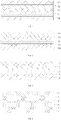
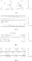
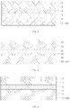
- FIGS. 1-16 respectively show different schematic views of thin film packaging structures according to the embodiments of the present disclosure.
- the thin film packaging structure may include a first inorganic packaging layer 10, an organic packaging layer 11, a second inorganic packaging layer 12, and at least one first inorganic adjusting layer 13.
- the first inorganic packaging layer 10 is used to cover a device to be packaged, where the device to be packaged may be an OLED device. That is to say, the OLED device may be packaged using the thin film packaging structure.
- the OLED device is packaged by the first inorganic packaging layer 10 to prevent water and oxygen from getting into the OLED device and thus, ensure the service life of the OLED device.
- the first inorganic packaging layer 10 may be made of silicon oxynitride.
- the silicon oxynitride may be deposited on a surface of the device to be packaged through the chemical vapor deposition (CVD) method to package the device.
- CVD chemical vapor deposition
- the organic packaging layer 11 may be formed at a side of the first inorganic packaging layer 10.
- the organic packaging layer 11 is provided, on one hand, to improve flatness of the thin film packaging structure and, on the other hand, to improve the bending capability of the entire thin film packaging structure.
- the organic packaging layer 11 may be an inkjet printing layer formed by inkjet printing with an organic liquid.
- the second inorganic packaging layer 12 may be formed at a side of the organic packaging layer 11 facing away from the first inorganic packaging layer 10.
- the second inorganic packaging layer 12 is provided to further improve the packaging effect of the thin film packaging structure.
- the second inorganic packaging layer 12 may be made of silicon nitride.
- the silicon nitride may be deposited on the organic packaging layer 11 by chemical vapor deposition.
- the first inorganic adjusting layer 13 may be formed at a side of the first inorganic packaging layer 10 facing away from the device to be packaged.
- An elasticity modulus of the first inorganic adjusting layer 13 is greater than elasticity modulus of the first inorganic packaging layer 10 and the second inorganic packaging layer 12.
- a first inorganic adjusting layer 13 having a greater elasticity modulus is provided at the side of the first inorganic packaging layer 10 facing away from the device to be packaged to increase the stability of the thin film packaging structure in a bending process to avoid the thin film packaging structure from being broken, or prevent separation between film layers, thereby ensuring the packaging stability of the film packaging structure, and thereby improving the bending performance and service life of the display panel.
- the thickness of the first inorganic adjusting layer 13 may be 10 nm to 100 nm, for example, 10 nm, 30 nm, 50 nm, 70 nm, 90 nm, 100 nm, etc., that is, the thickness of the first inorganic adjusting layer 13 may be between 10 nm and 100 nm.
- the thickness of the first inorganic adjusting layer 13 is designed to be between 10 nm and 100 nm, on one hand, to avoid the situation that the first inorganic adjusting layer 13 is too thin to adjust the position of the stress neutral layer, on the other hand, to avoid the situation that the first inorganic adjusting layer 13 is too thick and thus leading to lower light-emitting efficiency of the thin film package structure.
- the stress neutral layer includes the structure (e.g., surface) formed at all positions where the internal tangential stress is zero when the thin film packaging structure is bent and deformed.
- the first inorganic adjusting layer 13 may be made of silicon oxide.
- the silicon oxide may be deposited at a side of the first inorganic packaging layer 10 by chemical vapor deposition, and the silicon oxide has characteristics of high elasticity modulus, high transmission rate, and the like, so that the transmission rate of the thin film packaging structure may be improved while the structural stability of the thin film packaging structure is improved.
- silicon oxide is used as the first inorganic adjusting layer 13, and the thickness of the first inorganic adjusting layer 13 may be adjusted according to practical problems that occur in the bending process of the thin film packaging structure, so that the stress neutral layer at the bending position is closer to the inorganic packaging layer which is easy to be broken or separated.
- this embodiment may adjust the thickness of the first inorganic adjusting layer 13 according to the practical problems that occur in the bending process of the thin film packaging structure so that the stress neutral layer at the bending position may be closer to the inorganic packaging layer which is easy to be broken or separated. Also, the positional relationships between the first inorganic adjusting layer 13 and the first inorganic packaging layer 10 and the second inorganic packaging layer 12 may be adjusted according to the practical problems that occur in the bending process of the thin film packaging structure, so that the stress neutral layer at the bending position may be closer to the inorganic packaging layer which is easy to be broken or separated.
- the first inorganic adjusting layer 13 may be formed between the first inorganic packaging layer 10 and the organic packaging layer 11, so that the stress neutral layer at the bending position may be offset towards the first inorganic packaging layer 10, that is, the distance between the first inorganic packaging layer 10 and the stress neutral layer is reduced, as such, compared to the solution that the first inorganic packaging layer 10 is directly combined with the organic packaging layer 11 in the prior art, the deformation amount of the first inorganic packaging layer 10 may be reduced as reaching the same bending radius, to alleviate the situation that the first inorganic packaging layer 10 may be broken or separated from other film layers in the bending process, and further ensure the stability of the thin film packaging structure, so that the packaging effect of the thin film packaging structure can be improved.
- the first inorganic adjusting layer 13 is made of silicon oxide
- the first inorganic packaging layer 10 is made of silicon oxynitride
- an oxygen content of the first inorganic adjusting layer 13 is greater than an oxygen content of the first inorganic packaging layer 10, so that a contact angle between the first inorganic adjusting layer 13 and the organic packaging layer 11 is smaller than a contact angle between the first inorganic packaging layer 10 and the organic packaging layer 11. Therefore, after curing, a bonding strength between the first inorganic adjusting layer 13 and the organic packaging layer 11 is greater than a bonding strength between the first inorganic packaging layer 10 and the organic packaging layer 11.
- the first inorganic adjusting layer 13 is formed between the first inorganic packaging layer 10 and the organic packaging layer 11 to increase the combination stability between the first inorganic packaging layer 10 and the organic packaging layer 11, and avoid the interlayer separation between the first inorganic packaging layer 10 and the organic packaging layer 11, thereby ensuring the stability of the thin film packaging structure and improving the packaging effect of the thin film packaging structure.
- the oxygen content of the first inorganic adjusting layer 13 is greater than the oxygen content of the second inorganic packaging layer 12 so that the contact angle between the first inorganic adjusting layer 13 and the organic packaging layer 11 is smaller than the contact angle between the second inorganic packaging layer 12 and the organic packaging layer 11.
- the bonding strength between the first inorganic adjusting layer 13 and the organic packaging layer 11 may be greater than the bonding strength between the second inorganic packaging layer 12 and the organic packaging layer 11.
- the first inorganic adjusting layer 13 may also be formed between the second inorganic packaging layer 12 and the organic packaging layer 11, in comparison with the direct combination between the second inorganic packaging layer 12 and the organic packaging layer 11, the combination stability between the second inorganic packaging layer 12 and the organic packaging layer 11 may be increased, and the interlayer separation between the second inorganic packaging layer 12 and the organic packaging layer 11 may be avoided, so that the stability of the thin film packaging structure may be ensured, and the packaging effect of the thin film packaging structure may be improved.
- the stress neutral layer may be further offset towards the first inorganic packaging layer 10 or the second inorganic packaging layer 12 as described in this embodiment, to reduce the distance between the first or second inorganic packaging layer 10 or 12 and the stress neutral layer, and reduce the deformation amount of the first inorganic packaging layer 10 and/or the second inorganic packaging layer 12, thereby alleviating the situation that the first inorganic packaging layer 10 and/or the second inorganic packaging layer 12 are/is broken or separated from other film layers in the bending process, and further ensuring the stability of the thin film packaging structure, such that the packaging effect of the thin film packaging structure can be improved.
- the thickness of the first inorganic adjusting layer 13 between the second inorganic packaging layer 12 and the organic packaging layer 11 may be smaller than the thickness of the first inorganic adjusting layer 13 between the first inorganic packaging layer 10 and the organic packaging layer 11, but is not limited thereto, and may be greater than or equal to the thickness of the first inorganic adjusting layer 13 between the first inorganic packaging layer 10 and the organic packaging layer 11 according to the specific situations.
- the first inorganic adjusting layer 13 may be formed between the second inorganic packaging layer 12 and the organic packaging layer 11, as shown in FIG. 3 ; or the first inorganic adjusting layer 13 is formed at a side of the second inorganic packaging layer 12 facing away from the organic packaging layer 11, as shown in FIG.
- first inorganic adjusting layer 13 is formed between the second inorganic packaging layer 12 and the organic packaging layer 11, and another first inorganic adjusting layer 13 is formed at a side of the second inorganic packaging layer 12 facing away from the organic packaging layer 11, as shown in FIG. 5 .
- the stress neutral layer at the bending position may be offset towards the second inorganic packaging layer 12, i.e., the distance between the second inorganic packaging layer 12 and the stress neutral layer may be reduced, so that compared to the traditional manner that the second inorganic packaging layer 12 is directly combined with the organic packaging layer 11, the deformation amount of the second inorganic packaging layer 12 may be reduced when the bending radius is consistent, alleviating the situation that the first inorganic packaging layer 10 may be broken or separated from other film layers in the bending process, and then ensuring the stability of the thin film packaging structure, so that the packaging effect of the thin film packaging structure may be improved.
- the oxygen content of the first inorganic adjusting layer 13 is greater than the oxygen content of the second inorganic packaging layer 12, so that the contact angle between the first inorganic adjusting layer 13 and the organic packaging layer 11 is smaller than the contact angle between the second inorganic packaging layer 12 and the organic packaging layer 11. Therefore, after curing, the bonding strength between the first inorganic adjusting layer 13 and the organic packaging layer 11 is greater than the bonding strength between the second inorganic packaging layer 12 and the organic packaging layer 11.
- the first inorganic adjusting layer 13 is formed between the second inorganic packaging layer 12 and the organic packaging layer 11, and compared to the situation that the second inorganic packaging layer 12 is directly combined with the organic packaging layer 11, the combination stability between the second inorganic packaging layer 12 and the organic packaging layer 11 may be further increased, and the interlayer separation between the second inorganic packaging layer 12 and the organic packaging layer 11 may be avoided, thereby ensuring the stability of the thin film packaging structure, and improving the packaging effect of the thin film packaging structure.
- the oxygen content of the first inorganic adjusting layer 13 is greater than the oxygen content of the first inorganic packaging layer 10, so that the contact angle between the first inorganic adjusting layer 13 and the organic packaging layer 11 is smaller than the contact angle between the first inorganic packaging layer 10 and the organic packaging layer 11.
- the bonding strength between the first inorganic adjusting layer 13 and the organic packaging layer 11 is greater than the bonding strength between the first inorganic packaging layer 10 and the organic packaging layer 11.
- a first inorganic adjusting layer 13 may also be formed between the first inorganic packaging layer 10 and the organic packaging layer 11, which may increase the combination stability between the first inorganic packaging layer 10 and the organic packaging layer 11, and may prevent the first inorganic packaging layer 10 and the organic packaging layer 11 from being separated from each other, thereby ensuring the stability of the thin film packaging structure and improving the packaging effect of the thin film packaging structure, compared to the situation that the first inorganic packaging layer 10 is directly combined with the organic packaging layer 11.
- the stress neutral layer of this embodiment may be further offset towards the first inorganic packaging layer 10 or the second inorganic packaging layer 12, so as to reduce the distance between the first inorganic packaging layer 10 or the second inorganic packaging layer 12 and the stress neutral layer, reduce the deformation amount of the first inorganic packaging layer 10 or the second inorganic packaging layer 12, and alleviate the situation that the first inorganic packaging layer 10 or the second inorganic packaging layer 12 is broken or separated from other film layers in the bending process, thereby ensuring the stability of the thin film packaging structure, and improving the packaging effect of the thin film packaging structure.
- the thickness of the first inorganic adjusting layer 13 between the first inorganic packaging layer 10 and the organic packaging layer 11 may be smaller than the thickness of the first inorganic adjusting layer 13 between the second inorganic packaging layer 12 and the organic packaging layer 11, but is not limited thereto, and may be greater than or equal to the thickness of the first inorganic adjusting layer 13 between the second inorganic packaging layer 12 and the organic packaging layer 11 according to the specific situations.
- a first inorganic adjusting layer 13 is also provided at a side of the first inorganic packaging layer 10 facing towards the device to be packaged.
- the first inorganic adjusting layer 13 is provided so that the stress neutral layer may be offset towards the first inorganic packaging layer 10, or may be offset towards the first inorganic packaging layer 10 and the second inorganic packaging layer 12 at the same time, depending on an initial position of the stress neutral layer, so as to alleviate the situation that the first inorganic packaging layer 10 and the second inorganic packaging layer 12 are broken or separated from other film layers during the bending process, and ensure the stability of the thin film packaging structure, and improve the packaging effect of the thin film packaging structure.
- the first inorganic adjusting layer 13 of some embodiments is made of silicon oxide, which does not absorb water and has a good capability of blocking water and oxygen, so as to further prevent water and oxygen from getting into the device to be packaged, thereby improving the reliability of the product.
- the silicon oxide has lower refractive index, and the light extraction efficiency is not influenced.
- a second inorganic adjusting layer 14 is provided at a side of the first inorganic packaging layer 10 facing towards the device to be packaged.
- the refractive index of the second inorganic adjusting layer 14 is lower than the refractive index of the first inorganic packaging layer 10, and for example, the second inorganic adjusting layer 14 may be made of lithium fluoride.
- the light emitting efficiency of the display panel may be improved.
- the first inorganic adjusting layer 13 of any of the above embodiments is not limited to silicon oxide, but may also be silicon oxynitride, as long as the oxygen content of the first inorganic adjusting layer 13 is greater than that of the first inorganic packaging layer 10 to achieve characteristics of high elasticity modulus and high bonding strength.
- the oxygen content of at least one first inorganic adjusting layer 13 is greater than that of the first inorganic packaging layer 10 and/or the second inorganic packaging layer 12. For example, as shown in FIG.
- the oxygen content of the first inorganic adjusting layer 13 between the first inorganic packaging layer 10 and the organic packaging layer 11 is greater than that of the first inorganic packaging layer 10 and the second inorganic packaging layer 12, so that the contact angle between the first inorganic adjusting layer 13 and the organic packaging layer 11 is smaller than that between the first inorganic packaging layer 10 and the organic packaging layer 11, in this way, the bonding strength between the first inorganic adjusting layer 13 and the first inorganic packaging layer 10 is increased, and the stability of the thin film packaging structure in the bending process is increased, so that the thin film packaging structure is prevented from being broken or separating between the film layers, and the packaging stability of the thin film packaging structure is ensured, thereby improving the bending performance and service life of the display panel.
- the oxygen content of the first inorganic adjusting layer located between the first inorganic packaging layer and the organic packaging layer is greater than that of the first inorganic packaging layer; the oxygen content of the first inorganic adjusting layer located between the second inorganic packaging layer and the organic packaging layer is greater than that of the second inorganic packaging layer.
- the oxygen content of the first inorganic adjusting layer 13 located between the first inorganic packaging layer 10 and the organic packaging layer 11 is greater than that of the first inorganic packaging layer 10.
- the contact angle between the first inorganic adjusting layer 13, which is located between the first inorganic packaging layer 10 and the organic packaging layer 11, and the organic packaging layer 11 is smaller than that between the first inorganic packaging layer 10 and the organic packaging layer 11, and thus after curing, the bonding strength between the first inorganic adjusting layer 13, which is located between the first inorganic packaging layer 10 and the organic packaging layer 11, and the organic packaging layer 11 is greater than that between the first inorganic packaging layer 10 and the organic packaging layer 11.
- the oxygen content of the first inorganic adjusting layer 13 located between the second inorganic packaging layer 12 and the organic packaging layer 11 is greater than that of the second inorganic packaging layer 12.
- the contact angle between the first inorganic adjusting layer 13, which is located between the second inorganic packaging layer 12 and the organic packaging layer 11, and the organic packaging layer 11 is smaller than that between the second inorganic packaging layer 12 and the organic packaging layer 11, and thus after curing, the bonding strength between the first inorganic adjusting layer 13, which is located between the second inorganic packaging layer 12 and the organic packaging layer 11, and the organic packaging layer 11 is greater than that between the second inorganic packaging layer 12 and the organic packaging layer 11.
- the material of the first inorganic packaging layer 10 includes silicon oxynitride.
- the silicon oxynitride may be deposited on the surface of the device to be packaged by CVD (Chemical Vapor Deposition) to realize the packaging of the device to be packaged.
- the material of the second inorganic packaging layer 12 includes silicon nitride.
- the silicon nitride may be deposited on the organic packaging layer 11 by chemical vapor deposition.
- the material of the first inorganic adjusting layer 13 located between the second inorganic packaging layer 12 and the organic packaging layer 11 includes silicon oxide or silicon oxynitride.
- the material of the first inorganic adjusting layer 13 located between the second inorganic packaging layer 12 and the organic packaging layer 11 includes silicon oxide. Silicon oxide has the characteristics of high elasticity modulus, high transmission rate, etc., which can improve the transmission rate of thin film packaging structure while improving the structural stability.
- the oxygen content of the material (such as silicon oxide) of the first inorganic adjusting layer 13 between the second inorganic packaging layer 12 and the organic packaging layer 11 is greater than that of the material (such as silicon nitride) of the second inorganic packaging layer 12.
- the bonding strength between the first inorganic adjusting layer 13 and the second inorganic packaging layer 12 is increased.
- the material of the first inorganic adjusting layer 13 between the first inorganic packaging layer 10 and the organic packaging layer 11 includes silicon oxynitride or silicon oxide.
- the material of the first inorganic adjusting layer 13 located between the first inorganic packaging layer 10 and the organic packaging layer 11 includes silicon oxynitride.
- the oxygen content of the material (such as silicon oxynitride) of the first inorganic adjusting layer 13 between the first inorganic packaging layer 10 and the organic packaging layer 11 is greater than that of the material (such as silicon oxynitride) of the first inorganic packaging layer 10. Therefore, the bonding strength between the first inorganic adjusting layer 13 and the first inorganic packaging layer 10 is increased.
- the thickness of the first inorganic adjusting layer 13 located between the first inorganic packaging layer 10 and the organic packaging layer 11 is greater than that of the first inorganic adjusting layer 13 located between the second inorganic packaging layer 12 and the organic packaging layer 11, so that the stress neutral layer at the bending position is closer to the inorganic packaging layer which is easy to be broken or separated, such as the first inorganic packaging layer 10.
- the material of the first inorganic adjusting layer 13 between the first inorganic packaging layer 10 and the organic packaging layer 11 is the same as that of the first inorganic packaging layer 10.
- the material of the first inorganic adjusting layer 13, which is located between the first inorganic packaging layer 10 and the organic packaging layer 11, and the material of the first inorganic packaging layer 10 both include silicon oxynitride.
- the oxygen content of silicon oxynitride of the first inorganic adjusting layer 13 located between the first inorganic packaging layer 10 and the organic packaging layer 11 is greater than that of the silicon oxynitride of the first inorganic packaging layer 10. Therefore, the bonding strength between the first inorganic adjusting layer 13 and the first inorganic packaging layer 10 is increased.
- the material of the first inorganic adjusting layer 13 located between the second inorganic packaging layer 12 and the organic packaging layer 11 is different from that of the second inorganic packaging layer 12.
- the material of the first inorganic adjusting layer 13 between the second inorganic packaging layer 12 and the organic packaging layer 11 includes silicon oxide
- the material of the second inorganic packaging layer 12 includes silicon nitride, so that the oxygen content of the first inorganic adjusting layer 13 between the second inorganic packaging layer 12 and the organic packaging layer 11 is greater than that of the second inorganic packaging layer 12.
- the stability of the thin film packaging structure in the bending process is increased, so that the thin film packaging structure is prevented from beign broken or separating between the film layers, and the packaging stability of the thin film packaging structure is ensured, thereby improving the bending performance and service life of the display panel.
- At least one embodiment of the present disclosure provides a display panel, which can be applied to display apparatuses such as mobile phones, computers and the like.
- the display panel may include a device to be packaged (not shown in the figures) and a thin film packaging structure for packaging the device to be packaged, the device to be packaged may be an OLED display device, and the thin film packaging structure may be a thin film packaging structure described in any of the above embodiments, and details will not be repeated here.
- the display panel of the present embodiment may be a flexible display panel.
- the first inorganic adjusting layer with greater elasticity modulus is arranged on the side of the first inorganic packaging layer facing away from the device to be packaged, which increases the stability of the thin film packaging structure in the bending process, avoids the breakage of the thin film packaging structure or the separation between the film layers of the thin film packaging structure, ensures the packaging stability of the thin film packaging structure, and thus improves the bending performance and service life of the display panel.
Landscapes
- Chemical & Material Sciences (AREA)
- Inorganic Chemistry (AREA)
- Engineering & Computer Science (AREA)
- General Chemical & Material Sciences (AREA)
- Chemical Kinetics & Catalysis (AREA)
- Materials Engineering (AREA)
- Mechanical Engineering (AREA)
- Metallurgy (AREA)
- Organic Chemistry (AREA)
- Physics & Mathematics (AREA)
- Electroluminescent Light Sources (AREA)
- Laminated Bodies (AREA)
- Optics & Photonics (AREA)
- General Physics & Mathematics (AREA)
- Devices For Indicating Variable Information By Combining Individual Elements (AREA)
- Theoretical Computer Science (AREA)
- Nonlinear Science (AREA)
- Mathematical Physics (AREA)
- Crystallography & Structural Chemistry (AREA)
- Liquid Crystal (AREA)
Abstract
Description
- This application claims the benefit of, and claims priority to
Chinese Patent Application No. 201910812392.4, filed on August 30, 2019 - Embodiments of the disclosure relates to a thin film packaging structure and a display panel.
- With the continued expansion of the application field of flexible organic light-emitting diode (OLED) display panels, there are increased reliability requirements of flexible OLED devices in severe environments.
- At present, in order to prevent water and oxygen from getting into OLED devices, thin film packaging technologies are usually applied to perform packaging. A traditional thin film packaging structure includes inorganic layers and organic layers that are successively stacked. The inorganic layer of thin film packaging structure experiences greater stresses when it is bended, so that the inorganic layer may be easily broken. Alternatively, film layers of the thin film packaging structure may be easily separated, reducing the bendability of the display panel.
- It should be noted that the information disclosed in the above "Background" section is merely intended to reinforce understanding of the background technology of the present disclosure and, accordingly, the Background may include information that does not constitute the prior art as already known by an ordinary person skilled in the art.
- An objective of this disclosure is to provide a thin film packaging structure and a display panel, which have good bending performance.
- Some embodiments of the present disclosure provide a thin film packaging structure, which includes: a first inorganic packaging layer for covering a device to be packaged; an organic packaging layer provided at a side of the first inorganic packaging layer; a second inorganic packaging layer provided at a side of the organic packaging layer facing away from the first inorganic packaging layer; and at least one first inorganic adjusting layer provided at a side of the first inorganic packaging layer facing away from the device to be packaged. An oxygen content of the at least one first inorganic adjusting layer is greater than an oxygen content of the first inorganic packaging layer and/or the second inorganic packaging layer.
- For example, in one exemplary embodiment of the present disclosure, the at least one first inorganic adjusting layer is provided between the first inorganic packaging layer and the organic packaging layer.
- For example, in one exemplary embodiment of the present disclosure, the at least one first inorganic adjusting layer is provided between the organic packaging layer and the second inorganic packaging layer.
- For example, in one exemplary embodiment of the present disclosure, the at least one first inorganic adjusting layer is provided at a side of the second inorganic packaging layer facing away from the organic packaging layer.
- For example, in one exemplary embodiment of the present disclosure, the at least one first inorganic adjusting layer is provided at a side of the first inorganic packaging layer facing towards the device to be packaged.
- For example, in one exemplary embodiment of the present disclosure, the thin film packaging structure further comprises: a second inorganic adjusting layer provided at a side of the first inorganic packaging layer facing towards the device to be packaged, and a refractive index of the second inorganic adjusting layer is lower than a refractive index of the first inorganic packaging layer.
- For example, in one exemplary embodiment of the present disclosure, the second inorganic adjusting layer is made of lithium fluoride.
- For example, in one exemplary embodiment of the present disclosure, the at least one first inorganic adjusting layer is made of silicon oxide.
- For example, in one exemplary embodiment of the present disclosure, the at least one first inorganic adjusting layer has a thickness of 10 nm to 100 nm.
- For example, in one exemplary embodiment of the present disclosure, the at least one first inorganic adjusting layer comprise two first inorganic adjusting layers, one of the two first inorganic adjusting layers is provided between the first inorganic packaging layer and the organic packaging layer, and the other of the two first inorganic adjusting layers is provided between the second inorganic packaging layer and the organic packaging layer.
- For example, in one exemplary embodiment of the present disclosure, the oxygen content of the one of the two first inorganic adjusting layers provided between the first inorganic packaging layer and the organic packaging layer is greater than the oxygen content of the first inorganic packaging layer; the oxygen content of the other of the two first inorganic adjusting layers provided between the second inorganic packaging layer and the organic packaging layer is greater than the oxygen content of the second inorganic packaging layer.
- For example, in one exemplary embodiment of the present disclosure, a thickness of the one of the two first inorganic adjusting layers provided between the first inorganic packaging layer and the organic packaging layer is greater than a thickness of the other of the two first inorganic adjusting layers provided between the second inorganic packaging layer and the organic packaging layer.
- For example, in one exemplary embodiment of the present disclosure, a material of the one of the two first inorganic adjusting layers provided between the first inorganic packaging layer and the organic packaging layer is the same as a material of the first inorganic packaging layer.
- For example, in one exemplary embodiment of the present disclosure, a material of the other of the two first inorganic adjusting layers provided between the second inorganic packaging layer and the organic packaging layer is different from a material of the second inorganic packaging layer.
- For example, in one exemplary embodiment of the present disclosure, a material of the first inorganic packaging layer includes silicon oxynitride.
- For example, in one exemplary embodiment of the present disclosure, a material of the second inorganic packaging layer includes silicon nitride.
- For example, in one exemplary embodiment of the present disclosure, a material of the other of the two first inorganic adjusting layers provided between the second inorganic packaging layer and the organic packaging layer includes silicon oxide.
- For example, in one exemplary embodiment of the present disclosure, a material of the one of the two first inorganic adjusting layers provided between the first inorganic packaging layer and the organic packaging layer includes silicon oxynitride.
- Some embodiments of the present disclosure provide a display panel, which includes: the device to be packaged; and the thin film packaging structure of any one of the above embodiments.
- For example, in one exemplary embodiment of the present disclosure, the device to be packaged is an OLED device.
- It should be understood that both the foregoing general description and the following detailed description are exemplary and explanatory only and are not restrictive of the disclosure.
- The accompanying drawings, which are incorporated in and constitute a part of this specification, illustrate embodiments consistent with the present disclosure and together with the description, serve to explain the principles of the present disclosure. It should be apparent that the drawings in the following description are merely examples of this disclosure, and that other drawings may also be obtained by those ordinary skilled in the art without creative work.
-
FIGS. 1-16 respectively show different schematic views of thin film packaging structures according to the embodiments of the present disclosure. - 10- first inorganic packaging layer; 11- organic packaging layer; 12- second inorganic packaging layer; 13- first inorganic adjusting layer; 14- second inorganic adjusting layer.
- Now, the exemplary embodiments will be described more fully with reference to the accompanying drawings. However, the exemplary embodiments can be embodied in a variety of forms and should not be construed as limiting the embodiments set forth herein. Instead, these embodiments are provided so that the present disclosure will be thorough and complete, and the concepts of the exemplary embodiments will be fully given to those skilled in the art. The same reference numerals denote the same or similar structures in the drawings, and thus their detailed descriptions will be omitted.
- Although relative terms such as "above" and "under" are used herein to describe the relationship of one component relative to another component, such terms are used herein only for the sake of convenience, for example, in the direction shown in the figure, it should be understood that if the referenced device is inversed upside down, a component described as "above" will become a component described as "under." When a structure is described as "above" another structure, it probably means that the structure is integrally formed on another structure, or, the structure is "directly" disposed on another structure, or, the structure is "indirectly" disposed on another structure through an additional structure.
- Embodiments of the present disclosure provide a thin film packaging structure, which has certain bendability. Specifically, as shown in
FIGS. 1-16 , the thin film packaging structure may include a firstinorganic packaging layer 10, anorganic packaging layer 11, a secondinorganic packaging layer 12, and at least one firstinorganic adjusting layer 13. - The first
inorganic packaging layer 10 is used to cover a device to be packaged, where the device to be packaged may be an OLED device. That is to say, the OLED device may be packaged using the thin film packaging structure. The OLED device is packaged by the firstinorganic packaging layer 10 to prevent water and oxygen from getting into the OLED device and thus, ensure the service life of the OLED device. - For example, the first
inorganic packaging layer 10 may be made of silicon oxynitride. The silicon oxynitride may be deposited on a surface of the device to be packaged through the chemical vapor deposition (CVD) method to package the device. - For example, in some embodiments, the
organic packaging layer 11 may be formed at a side of the firstinorganic packaging layer 10. Theorganic packaging layer 11 is provided, on one hand, to improve flatness of the thin film packaging structure and, on the other hand, to improve the bending capability of the entire thin film packaging structure. For example, theorganic packaging layer 11 may be an inkjet printing layer formed by inkjet printing with an organic liquid. The secondinorganic packaging layer 12 may be formed at a side of theorganic packaging layer 11 facing away from the firstinorganic packaging layer 10. The secondinorganic packaging layer 12 is provided to further improve the packaging effect of the thin film packaging structure. For example, the secondinorganic packaging layer 12 may be made of silicon nitride. The silicon nitride may be deposited on theorganic packaging layer 11 by chemical vapor deposition. - For example, in some embodiments, the first
inorganic adjusting layer 13 may be formed at a side of the firstinorganic packaging layer 10 facing away from the device to be packaged. An elasticity modulus of the firstinorganic adjusting layer 13 is greater than elasticity modulus of the firstinorganic packaging layer 10 and the secondinorganic packaging layer 12. In this embodiment, a firstinorganic adjusting layer 13 having a greater elasticity modulus is provided at the side of the firstinorganic packaging layer 10 facing away from the device to be packaged to increase the stability of the thin film packaging structure in a bending process to avoid the thin film packaging structure from being broken, or prevent separation between film layers, thereby ensuring the packaging stability of the film packaging structure, and thereby improving the bending performance and service life of the display panel. - For example, in some embodiments, the thickness of the first
inorganic adjusting layer 13 may be 10 nm to 100 nm, for example, 10 nm, 30 nm, 50 nm, 70 nm, 90 nm, 100 nm, etc., that is, the thickness of the firstinorganic adjusting layer 13 may be between 10 nm and 100 nm. In this embodiment, the thickness of the firstinorganic adjusting layer 13 is designed to be between 10 nm and 100 nm, on one hand, to avoid the situation that the firstinorganic adjusting layer 13 is too thin to adjust the position of the stress neutral layer, on the other hand, to avoid the situation that the firstinorganic adjusting layer 13 is too thick and thus leading to lower light-emitting efficiency of the thin film package structure. - For example, in the embodiments of the present disclosure, the stress neutral layer includes the structure (e.g., surface) formed at all positions where the internal tangential stress is zero when the thin film packaging structure is bent and deformed.
- For example, in some embodiments, the first
inorganic adjusting layer 13 may be made of silicon oxide. The silicon oxide may be deposited at a side of the firstinorganic packaging layer 10 by chemical vapor deposition, and the silicon oxide has characteristics of high elasticity modulus, high transmission rate, and the like, so that the transmission rate of the thin film packaging structure may be improved while the structural stability of the thin film packaging structure is improved. In addition, since the thickness of the silicon oxide is easy to be controlled, silicon oxide is used as the firstinorganic adjusting layer 13, and the thickness of the firstinorganic adjusting layer 13 may be adjusted according to practical problems that occur in the bending process of the thin film packaging structure, so that the stress neutral layer at the bending position is closer to the inorganic packaging layer which is easy to be broken or separated. - It should be noted that, this embodiment may adjust the thickness of the first
inorganic adjusting layer 13 according to the practical problems that occur in the bending process of the thin film packaging structure so that the stress neutral layer at the bending position may be closer to the inorganic packaging layer which is easy to be broken or separated. Also, the positional relationships between the firstinorganic adjusting layer 13 and the firstinorganic packaging layer 10 and the secondinorganic packaging layer 12 may be adjusted according to the practical problems that occur in the bending process of the thin film packaging structure, so that the stress neutral layer at the bending position may be closer to the inorganic packaging layer which is easy to be broken or separated. - The structure of the thin film packaging structure will be described in detail below with reference to the accompanying drawings.
- For example, in some embodiments of the present disclosure, if the first
inorganic packaging layer 10 of the thin film packaging structure is more easily broken or separated from other film layers during the actual bending process of the display panel, as shown inFIG. 1 , the firstinorganic adjusting layer 13 may be formed between the firstinorganic packaging layer 10 and theorganic packaging layer 11, so that the stress neutral layer at the bending position may be offset towards the firstinorganic packaging layer 10, that is, the distance between the firstinorganic packaging layer 10 and the stress neutral layer is reduced, as such, compared to the solution that the firstinorganic packaging layer 10 is directly combined with theorganic packaging layer 11 in the prior art, the deformation amount of the firstinorganic packaging layer 10 may be reduced as reaching the same bending radius, to alleviate the situation that the firstinorganic packaging layer 10 may be broken or separated from other film layers in the bending process, and further ensure the stability of the thin film packaging structure, so that the packaging effect of the thin film packaging structure can be improved. - It should be noted that, when the first
inorganic adjusting layer 13 is made of silicon oxide, and the firstinorganic packaging layer 10 is made of silicon oxynitride, an oxygen content of the firstinorganic adjusting layer 13 is greater than an oxygen content of the firstinorganic packaging layer 10, so that a contact angle between the firstinorganic adjusting layer 13 and theorganic packaging layer 11 is smaller than a contact angle between the firstinorganic packaging layer 10 and theorganic packaging layer 11. Therefore, after curing, a bonding strength between the firstinorganic adjusting layer 13 and theorganic packaging layer 11 is greater than a bonding strength between the firstinorganic packaging layer 10 and theorganic packaging layer 11. - In this embodiment, compared with the situation that the first
inorganic packaging layer 10 is directly combined with theorganic packaging layer 11, the firstinorganic adjusting layer 13 is formed between the firstinorganic packaging layer 10 and theorganic packaging layer 11 to increase the combination stability between the firstinorganic packaging layer 10 and theorganic packaging layer 11, and avoid the interlayer separation between the firstinorganic packaging layer 10 and theorganic packaging layer 11, thereby ensuring the stability of the thin film packaging structure and improving the packaging effect of the thin film packaging structure. - For example, in some embodiments of the present disclosure, when the first
inorganic adjusting layer 13 is made of silicon oxide, and the secondinorganic packaging layer 12 is made of silicon nitride, the oxygen content of the firstinorganic adjusting layer 13 is greater than the oxygen content of the secondinorganic packaging layer 12 so that the contact angle between the firstinorganic adjusting layer 13 and theorganic packaging layer 11 is smaller than the contact angle between the secondinorganic packaging layer 12 and theorganic packaging layer 11. After curing, the bonding strength between the firstinorganic adjusting layer 13 and theorganic packaging layer 11 may be greater than the bonding strength between the secondinorganic packaging layer 12 and theorganic packaging layer 11. - For example, in some embodiments, as shown in
FIG. 2 , compared to the previous embodiment ofFIG. 1 , apart from that the firstinorganic adjusting layer 13 is formed between the firstinorganic packaging layer 10 and theorganic packaging layer 11, the firstinorganic adjusting layer 13 may also be formed between the secondinorganic packaging layer 12 and theorganic packaging layer 11, in comparison with the direct combination between the secondinorganic packaging layer 12 and theorganic packaging layer 11, the combination stability between the secondinorganic packaging layer 12 and theorganic packaging layer 11 may be increased, and the interlayer separation between the secondinorganic packaging layer 12 and theorganic packaging layer 11 may be avoided, so that the stability of the thin film packaging structure may be ensured, and the packaging effect of the thin film packaging structure may be improved. - It should be noted that, in the actual bending process, if the stress neutral layer is at a side of the first
inorganic packaging layer 10 or the secondinorganic packaging layer 12, the stress neutral layer may be further offset towards the firstinorganic packaging layer 10 or the secondinorganic packaging layer 12 as described in this embodiment, to reduce the distance between the first or secondinorganic packaging layer inorganic packaging layer 10 and/or the secondinorganic packaging layer 12, thereby alleviating the situation that the firstinorganic packaging layer 10 and/or the secondinorganic packaging layer 12 are/is broken or separated from other film layers in the bending process, and further ensuring the stability of the thin film packaging structure, such that the packaging effect of the thin film packaging structure can be improved. - It should be noted that the thickness of the first
inorganic adjusting layer 13 between the secondinorganic packaging layer 12 and theorganic packaging layer 11 may be smaller than the thickness of the firstinorganic adjusting layer 13 between the firstinorganic packaging layer 10 and theorganic packaging layer 11, but is not limited thereto, and may be greater than or equal to the thickness of the firstinorganic adjusting layer 13 between the firstinorganic packaging layer 10 and theorganic packaging layer 11 according to the specific situations. - For example, in some embodiments of the present disclosure, if the second
inorganic packaging layer 12 of the thin film packaging structure is more likely to be broken or separated from other film layers during the actual bending process of the display panel, the firstinorganic adjusting layer 13 may be formed between the secondinorganic packaging layer 12 and theorganic packaging layer 11, as shown inFIG. 3 ; or the firstinorganic adjusting layer 13 is formed at a side of the secondinorganic packaging layer 12 facing away from theorganic packaging layer 11, as shown inFIG. 4 ; or a firstinorganic adjusting layer 13 is formed between the secondinorganic packaging layer 12 and theorganic packaging layer 11, and another firstinorganic adjusting layer 13 is formed at a side of the secondinorganic packaging layer 12 facing away from theorganic packaging layer 11, as shown inFIG. 5 . With these solutions, the stress neutral layer at the bending position may be offset towards the secondinorganic packaging layer 12, i.e., the distance between the secondinorganic packaging layer 12 and the stress neutral layer may be reduced, so that compared to the traditional manner that the secondinorganic packaging layer 12 is directly combined with theorganic packaging layer 11, the deformation amount of the secondinorganic packaging layer 12 may be reduced when the bending radius is consistent, alleviating the situation that the firstinorganic packaging layer 10 may be broken or separated from other film layers in the bending process, and then ensuring the stability of the thin film packaging structure, so that the packaging effect of the thin film packaging structure may be improved. - It should be noted that, when the first
inorganic adjusting layer 13 is made of silicon oxide and the secondinorganic packaging layer 12 is made of silicon nitride, the oxygen content of the firstinorganic adjusting layer 13 is greater than the oxygen content of the secondinorganic packaging layer 12, so that the contact angle between the firstinorganic adjusting layer 13 and theorganic packaging layer 11 is smaller than the contact angle between the secondinorganic packaging layer 12 and theorganic packaging layer 11. Therefore, after curing, the bonding strength between the firstinorganic adjusting layer 13 and theorganic packaging layer 11 is greater than the bonding strength between the secondinorganic packaging layer 12 and theorganic packaging layer 11. - In the embodiment, the first
inorganic adjusting layer 13 is formed between the secondinorganic packaging layer 12 and theorganic packaging layer 11, and compared to the situation that the secondinorganic packaging layer 12 is directly combined with theorganic packaging layer 11, the combination stability between the secondinorganic packaging layer 12 and theorganic packaging layer 11 may be further increased, and the interlayer separation between the secondinorganic packaging layer 12 and theorganic packaging layer 11 may be avoided, thereby ensuring the stability of the thin film packaging structure, and improving the packaging effect of the thin film packaging structure. - For example, in some embodiments of the present disclosure, when the first
inorganic adjusting layer 13 is made of silicon oxide, and the firstinorganic packaging layer 10 is made of silicon oxynitride, the oxygen content of the firstinorganic adjusting layer 13 is greater than the oxygen content of the firstinorganic packaging layer 10, so that the contact angle between the firstinorganic adjusting layer 13 and theorganic packaging layer 11 is smaller than the contact angle between the firstinorganic packaging layer 10 and theorganic packaging layer 11. After curing, the bonding strength between the firstinorganic adjusting layer 13 and theorganic packaging layer 11 is greater than the bonding strength between the firstinorganic packaging layer 10 and theorganic packaging layer 11. - For example, in some embodiments, as shown in
FIGS. 6 to 8 , compared to the previous embodiments (seeFIGS. 3 to 5 ), in addition to forming the firstinorganic adjusting layer 13 between the secondinorganic packaging layer 12 and theorganic packaging layer 11, and/or in addition to forming the firstinorganic adjusting layer 13 at a side of the secondinorganic packaging layer 12 facing away from theorganic packaging layer 11, a firstinorganic adjusting layer 13 may also be formed between the firstinorganic packaging layer 10 and theorganic packaging layer 11, which may increase the combination stability between the firstinorganic packaging layer 10 and theorganic packaging layer 11, and may prevent the firstinorganic packaging layer 10 and theorganic packaging layer 11 from being separated from each other, thereby ensuring the stability of the thin film packaging structure and improving the packaging effect of the thin film packaging structure, compared to the situation that the firstinorganic packaging layer 10 is directly combined with theorganic packaging layer 11. - It should be noted that, in the actual bending process, if the stress neutral layer is at a side of the first
inorganic packaging layer 10 or the secondinorganic packaging layer 12, the stress neutral layer of this embodiment may be further offset towards the firstinorganic packaging layer 10 or the secondinorganic packaging layer 12, so as to reduce the distance between the firstinorganic packaging layer 10 or the secondinorganic packaging layer 12 and the stress neutral layer, reduce the deformation amount of the firstinorganic packaging layer 10 or the secondinorganic packaging layer 12, and alleviate the situation that the firstinorganic packaging layer 10 or the secondinorganic packaging layer 12 is broken or separated from other film layers in the bending process, thereby ensuring the stability of the thin film packaging structure, and improving the packaging effect of the thin film packaging structure. - It should be noted that, the thickness of the first
inorganic adjusting layer 13 between the firstinorganic packaging layer 10 and theorganic packaging layer 11 may be smaller than the thickness of the firstinorganic adjusting layer 13 between the secondinorganic packaging layer 12 and theorganic packaging layer 11, but is not limited thereto, and may be greater than or equal to the thickness of the firstinorganic adjusting layer 13 between the secondinorganic packaging layer 12 and theorganic packaging layer 11 according to the specific situations. - For example, in some embodiments of the present disclosure, as shown in
FIGS. 9-16 , the main difference from any of the previous embodiments ofFIGS. 1 to 8 is that, a firstinorganic adjusting layer 13 is also provided at a side of the firstinorganic packaging layer 10 facing towards the device to be packaged. The firstinorganic adjusting layer 13 is provided so that the stress neutral layer may be offset towards the firstinorganic packaging layer 10, or may be offset towards the firstinorganic packaging layer 10 and the secondinorganic packaging layer 12 at the same time, depending on an initial position of the stress neutral layer, so as to alleviate the situation that the firstinorganic packaging layer 10 and the secondinorganic packaging layer 12 are broken or separated from other film layers during the bending process, and ensure the stability of the thin film packaging structure, and improve the packaging effect of the thin film packaging structure. - For example, the first
inorganic adjusting layer 13 of some embodiments is made of silicon oxide, which does not absorb water and has a good capability of blocking water and oxygen, so as to further prevent water and oxygen from getting into the device to be packaged, thereby improving the reliability of the product. Also, the silicon oxide has lower refractive index, and the light extraction efficiency is not influenced. - For example, in some embodiments, as shown in
FIGS. 9-16 , the main difference from any of the previous embodiments (seeFIGS. 1 to 8 ) is that, a secondinorganic adjusting layer 14 is provided at a side of the firstinorganic packaging layer 10 facing towards the device to be packaged. The refractive index of the secondinorganic adjusting layer 14 is lower than the refractive index of the firstinorganic packaging layer 10, and for example, the secondinorganic adjusting layer 14 may be made of lithium fluoride. - When the thin film packaging structure of the embodiments is applied to package a display device, the light emitting efficiency of the display panel may be improved.
- It should be noted that the first
inorganic adjusting layer 13 of any of the above embodiments is not limited to silicon oxide, but may also be silicon oxynitride, as long as the oxygen content of the firstinorganic adjusting layer 13 is greater than that of the firstinorganic packaging layer 10 to achieve characteristics of high elasticity modulus and high bonding strength. - For example, in some embodiments, as shown in
FIGS. 1 to 16 , the oxygen content of at least one firstinorganic adjusting layer 13 is greater than that of the firstinorganic packaging layer 10 and/or the secondinorganic packaging layer 12. For example, as shown inFIG. 1 , the oxygen content of the firstinorganic adjusting layer 13 between the firstinorganic packaging layer 10 and theorganic packaging layer 11 is greater than that of the firstinorganic packaging layer 10 and the secondinorganic packaging layer 12, so that the contact angle between the firstinorganic adjusting layer 13 and theorganic packaging layer 11 is smaller than that between the firstinorganic packaging layer 10 and theorganic packaging layer 11, in this way, the bonding strength between the firstinorganic adjusting layer 13 and the firstinorganic packaging layer 10 is increased, and the stability of the thin film packaging structure in the bending process is increased, so that the thin film packaging structure is prevented from being broken or separating between the film layers, and the packaging stability of the thin film packaging structure is ensured, thereby improving the bending performance and service life of the display panel. - For example, in some embodiments, the oxygen content of the first inorganic adjusting layer located between the first inorganic packaging layer and the organic packaging layer is greater than that of the first inorganic packaging layer; the oxygen content of the first inorganic adjusting layer located between the second inorganic packaging layer and the organic packaging layer is greater than that of the second inorganic packaging layer. As shown in
FIG. 2 , the oxygen content of the firstinorganic adjusting layer 13 located between the firstinorganic packaging layer 10 and theorganic packaging layer 11 is greater than that of the firstinorganic packaging layer 10. Therefore, the contact angle between the firstinorganic adjusting layer 13, which is located between the firstinorganic packaging layer 10 and theorganic packaging layer 11, and theorganic packaging layer 11 is smaller than that between the firstinorganic packaging layer 10 and theorganic packaging layer 11, and thus after curing, the bonding strength between the firstinorganic adjusting layer 13, which is located between the firstinorganic packaging layer 10 and theorganic packaging layer 11, and theorganic packaging layer 11 is greater than that between the firstinorganic packaging layer 10 and theorganic packaging layer 11. The oxygen content of the firstinorganic adjusting layer 13 located between the secondinorganic packaging layer 12 and theorganic packaging layer 11 is greater than that of the secondinorganic packaging layer 12. Therefore, the contact angle between the firstinorganic adjusting layer 13, which is located between the secondinorganic packaging layer 12 and theorganic packaging layer 11, and theorganic packaging layer 11 is smaller than that between the secondinorganic packaging layer 12 and theorganic packaging layer 11, and thus after curing, the bonding strength between the firstinorganic adjusting layer 13, which is located between the secondinorganic packaging layer 12 and theorganic packaging layer 11, and theorganic packaging layer 11 is greater than that between the secondinorganic packaging layer 12 and theorganic packaging layer 11. - For example, in some embodiments, as shown in
FIGS. 1 to 16 , the material of the firstinorganic packaging layer 10 includes silicon oxynitride. The silicon oxynitride may be deposited on the surface of the device to be packaged by CVD (Chemical Vapor Deposition) to realize the packaging of the device to be packaged. - For example, in some embodiments, as shown in
FIGS. 1 to 16 , the material of the secondinorganic packaging layer 12 includes silicon nitride. The silicon nitride may be deposited on theorganic packaging layer 11 by chemical vapor deposition. - For example, in some embodiments, as shown in
FIGS. 2-3 ,5-6 ,8 ,10-11 and13-16 , the material of the firstinorganic adjusting layer 13 located between the secondinorganic packaging layer 12 and theorganic packaging layer 11 includes silicon oxide or silicon oxynitride. For example, the material of the firstinorganic adjusting layer 13 located between the secondinorganic packaging layer 12 and theorganic packaging layer 11 includes silicon oxide. Silicon oxide has the characteristics of high elasticity modulus, high transmission rate, etc., which can improve the transmission rate of thin film packaging structure while improving the structural stability. The oxygen content of the material (such as silicon oxide) of the firstinorganic adjusting layer 13 between the secondinorganic packaging layer 12 and theorganic packaging layer 11 is greater than that of the material (such as silicon nitride) of the secondinorganic packaging layer 12. The bonding strength between the firstinorganic adjusting layer 13 and the secondinorganic packaging layer 12 is increased. - For example, in some embodiments, as shown in
FIGS. 1-2 ,6-10 and14-16 , the material of the firstinorganic adjusting layer 13 between the firstinorganic packaging layer 10 and theorganic packaging layer 11 includes silicon oxynitride or silicon oxide. For example, the material of the firstinorganic adjusting layer 13 located between the firstinorganic packaging layer 10 and theorganic packaging layer 11 includes silicon oxynitride. The oxygen content of the material (such as silicon oxynitride) of the firstinorganic adjusting layer 13 between the firstinorganic packaging layer 10 and theorganic packaging layer 11 is greater than that of the material (such as silicon oxynitride) of the firstinorganic packaging layer 10. Therefore, the bonding strength between the firstinorganic adjusting layer 13 and the firstinorganic packaging layer 10 is increased. - For example, in some embodiments, as shown in
FIG. 2 , the thickness of the firstinorganic adjusting layer 13 located between the firstinorganic packaging layer 10 and theorganic packaging layer 11 is greater than that of the firstinorganic adjusting layer 13 located between the secondinorganic packaging layer 12 and theorganic packaging layer 11, so that the stress neutral layer at the bending position is closer to the inorganic packaging layer which is easy to be broken or separated, such as the firstinorganic packaging layer 10. For example, in some embodiments, as shown inFIGS. 1-2 ,6-10 and14-16 , the material of the firstinorganic adjusting layer 13 between the firstinorganic packaging layer 10 and theorganic packaging layer 11 is the same as that of the firstinorganic packaging layer 10. For example, the material of the firstinorganic adjusting layer 13, which is located between the firstinorganic packaging layer 10 and theorganic packaging layer 11, and the material of the firstinorganic packaging layer 10 both include silicon oxynitride. For example, the oxygen content of silicon oxynitride of the firstinorganic adjusting layer 13 located between the firstinorganic packaging layer 10 and theorganic packaging layer 11 is greater than that of the silicon oxynitride of the firstinorganic packaging layer 10. Therefore, the bonding strength between the firstinorganic adjusting layer 13 and the firstinorganic packaging layer 10 is increased. - For example, in some embodiments, as shown in
FIGS. 2-3 ,5-6 ,8 ,10-11 and13-16 , the material of the firstinorganic adjusting layer 13 located between the secondinorganic packaging layer 12 and theorganic packaging layer 11 is different from that of the secondinorganic packaging layer 12. For example, the material of the firstinorganic adjusting layer 13 between the secondinorganic packaging layer 12 and theorganic packaging layer 11 includes silicon oxide, and the material of the secondinorganic packaging layer 12 includes silicon nitride, so that the oxygen content of the firstinorganic adjusting layer 13 between the secondinorganic packaging layer 12 and theorganic packaging layer 11 is greater than that of the secondinorganic packaging layer 12. Therefore, while ensuring the light transmission rate of the thin film packaging structure, the stability of the thin film packaging structure in the bending process is increased, so that the thin film packaging structure is prevented from beign broken or separating between the film layers, and the packaging stability of the thin film packaging structure is ensured, thereby improving the bending performance and service life of the display panel. - At least one embodiment of the present disclosure provides a display panel, which can be applied to display apparatuses such as mobile phones, computers and the like. The display panel may include a device to be packaged (not shown in the figures) and a thin film packaging structure for packaging the device to be packaged, the device to be packaged may be an OLED display device, and the thin film packaging structure may be a thin film packaging structure described in any of the above embodiments, and details will not be repeated here. The display panel of the present embodiment may be a flexible display panel.
- The technical solutions of the embodiments of the disclosure at least have the following beneficial effects.
- As for the thin film packaging structure and the display panel provided by the embodiments of the disclosure, the first inorganic adjusting layer with greater elasticity modulus is arranged on the side of the first inorganic packaging layer facing away from the device to be packaged, which increases the stability of the thin film packaging structure in the bending process, avoids the breakage of the thin film packaging structure or the separation between the film layers of the thin film packaging structure, ensures the packaging stability of the thin film packaging structure, and thus improves the bending performance and service life of the display panel.
- The terms "a," "an," "the," "said," and "at least one" are used to express the presence of one or more the element, component, or the like. The terms "comprise," "include," and "have" are intended to be inclusive, and mean there may be additional elements, components, or the like other than the listed elements, components, or the like. The terms "first" and "second" are used only as labels, and are not numerical restriction to the objects.
- Other embodiments of the disclosure will be apparent to those skilled in the art from consideration of the specification and practice of the disclosure disclosed herein. This application is intended to cover any variations, uses, or adaptations of the disclosure, in general, the principles of the disclosure and including such departures from the present disclosure as come within known or customary practice in the art to which the disclosure pertains. It is intended that the specification and examples be considered as exemplary only, with a true scope and spirit of the disclosure being indicated by the following claims.
Claims (20)
- A thin film packaging structure, comprising:a first inorganic packaging layer for covering a device to be packaged;an organic packaging layer provided at a side of the first inorganic packaging layer;a second inorganic packaging layer provided at a side of the organic packaging layer facing away from the first inorganic packaging layer; andat least one first inorganic adjusting layer provided at a side of the first inorganic packaging layer facing away from the device to be packaged, whereinan oxygen content of the at least one first inorganic adjusting layer is greater than an oxygen content of the first inorganic packaging layer and/or the second inorganic packaging layer.
- The thin film packaging structure of claim 1, wherein the at least one first inorganic adjusting layer is provided between the first inorganic packaging layer and the organic packaging layer.
- The thin film packaging structure of claim 1 or 2, wherein the at least one first inorganic adjusting layer is provided between the organic packaging layer and the second inorganic packaging layer.
- The thin film packaging structure of any one of claims 1-3, wherein the at least one first inorganic adjusting layer is provided at a side of the second inorganic packaging layer facing away from the organic packaging layer.
- The thin film packaging structure of any one of claims 1-4, wherein the at least one first inorganic adjusting layer is provided at a side of the first inorganic packaging layer facing towards the device to be packaged.
- The thin film packaging structure of any one claims 1-4, further comprising:
a second inorganic adjusting layer provided at a side of the first inorganic packaging layer facing towards the device to be packaged, wherein a refractive index of the second inorganic adjusting layer is lower than a refractive index of the first inorganic packaging layer. - The thin film packaging structure of claim 6, wherein the second inorganic adjusting layer is made of lithium fluoride.
- The thin film packaging structure of any one of claims 1-7, wherein the at least one first inorganic adjusting layer is made of silicon oxide.
- The thin film packaging structure of any one of claims 1-8, wherein the at least one first inorganic adjusting layer has a thickness of 10 nm to 100 nm.
- The thin film packaging structure of any one of claims 1-9, wherein the at least one first inorganic adjusting layer comprise two first inorganic adjusting layers, one of the two first inorganic adjusting layers is provided between the first inorganic packaging layer and the organic packaging layer, and the other of the two first inorganic adjusting layers is provided between the second inorganic packaging layer and the organic packaging layer.
- The thin film packaging structure of claim 10, wherein the oxygen content of the one of the two first inorganic adjusting layers provided between the first inorganic packaging layer and the organic packaging layer is greater than the oxygen content of the first inorganic packaging layer; the oxygen content of the other of the two first inorganic adjusting layers provided between the second inorganic packaging layer and the organic packaging layer is greater than the oxygen content of the second inorganic packaging layer.
- The thin film packaging structure of claim 10 or 11, wherein a thickness of the one of the two first inorganic adjusting layers provided between the first inorganic packaging layer and the organic packaging layer is greater than a thickness of the other of the two first inorganic adjusting layers provided between the second inorganic packaging layer and the organic packaging layer.
- The thin film packaging structure of any one of claims 10-12, wherein a material of the one of the two first inorganic adjusting layers provided between the first inorganic packaging layer and the organic packaging layer is the same as a material of the first inorganic packaging layer.
- The thin film packaging structure of any one of claims 10-12, wherein a material of the other of the two first inorganic adjusting layers provided between the second inorganic packaging layer and the organic packaging layer is different from a material of the second inorganic packaging layer.
- The thin film packaging structure of any one of claims 10-14, wherein a material of the first inorganic packaging layer includes silicon oxynitride.
- The thin film packaging structure of any one of claims 10-15, wherein a material of the second inorganic packaging layer includes silicon nitride.
- The thin film packaging structure of any one of claims 10-16, wherein a material of the other of the two first inorganic adjusting layers provided between the second inorganic packaging layer and the organic packaging layer includes silicon oxide.
- The thin film packaging structure of any one of claims 10-17, wherein a material of the one of the two first inorganic adjusting layers provided between the first inorganic packaging layer and the organic packaging layer includes silicon oxynitride.
- A display panel, comprising: the thin film packaging structure of any one of claims 1-18, and the device to be packaged.
- The display panel of claim 19, wherein the device to be packaged is an OLED device.
Applications Claiming Priority (2)
| Application Number | Priority Date | Filing Date | Title |
|---|---|---|---|
| CN201910812392.4A CN110518146B (en) | 2019-08-30 | 2019-08-30 | Thin film packaging structure and display panel |
| PCT/CN2020/112299 WO2021037254A1 (en) | 2019-08-30 | 2020-08-29 | Thin film encapsulation structure and display panel |
Publications (2)
| Publication Number | Publication Date |
|---|---|
| EP4024493A1 true EP4024493A1 (en) | 2022-07-06 |
| EP4024493A4 EP4024493A4 (en) | 2022-11-09 |
Family
ID=68629555
Family Applications (1)
| Application Number | Title | Priority Date | Filing Date |
|---|---|---|---|
| EP20824071.3A Pending EP4024493A4 (en) | 2019-08-30 | 2020-08-29 | THIN FILM ENCAPSULATION STRUCTURE AND DISPLAY PANEL |
Country Status (10)
| Country | Link |
|---|---|
| US (3) | US11581508B2 (en) |
| EP (1) | EP4024493A4 (en) |
| JP (2) | JP7544604B2 (en) |
| KR (4) | KR102521911B1 (en) |
| CN (1) | CN110518146B (en) |
| AU (1) | AU2020338944B2 (en) |
| BR (1) | BR112021012674A2 (en) |
| MX (1) | MX2021007940A (en) |
| RU (1) | RU2771519C1 (en) |
| WO (1) | WO2021037254A1 (en) |
Families Citing this family (9)
| Publication number | Priority date | Publication date | Assignee | Title |
|---|---|---|---|---|
| CN110518146B (en) * | 2019-08-30 | 2022-02-25 | 京东方科技集团股份有限公司 | Thin film packaging structure and display panel |
| CN110970572B (en) * | 2019-11-14 | 2025-06-17 | 京东方科技集团股份有限公司 | Packaging structure, display panel and display device |
| CN111063821B (en) * | 2019-12-05 | 2022-07-12 | 武汉华星光电半导体显示技术有限公司 | Thin film packaging structure and display panel |
| CN111028690B (en) * | 2019-12-25 | 2021-10-22 | 霸州市云谷电子科技有限公司 | Display screen and display screen processing method |
| CN111129096A (en) * | 2019-12-30 | 2020-05-08 | 武汉华星光电半导体显示技术有限公司 | Organic light emitting diode device and manufacturing method thereof |
| CN111785768A (en) * | 2020-08-25 | 2020-10-16 | 京东方科技集团股份有限公司 | Organic light-emitting display panel, preparation method and display device |
| KR20220060071A (en) * | 2020-11-03 | 2022-05-11 | 삼성디스플레이 주식회사 | Display device |
| CN114784208B (en) * | 2022-04-12 | 2023-11-28 | 深圳市华星光电半导体显示技术有限公司 | Display panel, manufacturing method thereof and display device |
| CN118475167A (en) * | 2024-04-03 | 2024-08-09 | 武汉华星光电半导体显示技术有限公司 | Display panel and display device |
Family Cites Families (69)
| Publication number | Priority date | Publication date | Assignee | Title |
|---|---|---|---|---|
| US6822264B2 (en) * | 2001-11-16 | 2004-11-23 | Semiconductor Energy Laboratory Co., Ltd. | Light emitting device |
| US8350466B2 (en) * | 2004-09-17 | 2013-01-08 | Semiconductor Energy Laboratory Co., Ltd. | Display device and manufacturing method thereof |
| JP4539547B2 (en) * | 2005-12-08 | 2010-09-08 | セイコーエプソン株式会社 | LIGHT EMITTING DEVICE, LIGHT EMITTING DEVICE MANUFACTURING METHOD, AND ELECTRONIC DEVICE |
| KR20100125674A (en) * | 2009-05-21 | 2010-12-01 | 삼성모바일디스플레이주식회사 | Organic light emitting device and method for manufacturing same |
| KR101359657B1 (en) * | 2009-12-30 | 2014-02-06 | 엘지디스플레이 주식회사 | Electronic Device and Organic Light Emitting Device, Protection Multilayer Structure |
| US9245904B2 (en) * | 2011-06-24 | 2016-01-26 | Sharp Kabushiki Kaisha | Active matrix substrate and display device including the same |
| KR101892711B1 (en) * | 2011-12-28 | 2018-08-29 | 삼성디스플레이 주식회사 | Organic light emitting display apparatus and the method for manufacturing the same |
| CN103325960B (en) * | 2012-03-23 | 2016-03-16 | 昆山工研院新型平板显示技术中心有限公司 | The film encapsulation method of organic optoelectronic device |
| KR101903056B1 (en) | 2012-07-24 | 2018-10-02 | 삼성디스플레이 주식회사 | Organic light emitting display apparatus and the method for manufacturing the same |
| US8598786B1 (en) * | 2012-10-23 | 2013-12-03 | Samsung Display Co., Ltd. | Organic light-emitting display apparatus having a hydroxyquinoline-based layer as part of the sealing structure and method of manufacturing the same |
| KR102048926B1 (en) * | 2012-11-19 | 2019-11-27 | 삼성디스플레이 주식회사 | Organic light emitting display apparatus and the manufacturing method thereof |
| US9349988B2 (en) * | 2012-11-20 | 2016-05-24 | Samsung Display Co., Ltd. | Organic light emitting display device |
| KR101453880B1 (en) * | 2012-11-29 | 2014-10-22 | 삼성디스플레이 주식회사 | Organic light emitting display apparatus and the method for manufacturing the same |
| JP6139196B2 (en) * | 2013-03-15 | 2017-05-31 | 株式会社ジャパンディスプレイ | ORGANIC ELECTROLUMINESCENT DISPLAY DEVICE AND METHOD FOR PRODUCING ORGANIC ELECTROLUMINESCENT DISPLAY DEVICE |
| KR102080011B1 (en) * | 2013-06-13 | 2020-02-24 | 삼성디스플레이 주식회사 | Display device and method for manufacturing the same |
| KR20150017991A (en) * | 2013-08-08 | 2015-02-23 | 삼성디스플레이 주식회사 | Display device comprising encapsulation film and method for inspecting the encapsulation film |
| KR102093393B1 (en) * | 2013-08-14 | 2020-03-26 | 삼성디스플레이 주식회사 | Organic light emitting display apparatus and the manufacturing method thereof |
| KR101673016B1 (en) * | 2013-08-27 | 2016-11-07 | 삼성디스플레이 주식회사 | Thin film encapsulation manufacturing device and manufacturing method of display apparatus using the same |
| TWI593139B (en) * | 2013-08-30 | 2017-07-21 | 旭化成電子材料股份有限公司 | Semiconductor light-emitting element and optical film |
| KR102116497B1 (en) * | 2013-09-25 | 2020-05-29 | 삼성디스플레이 주식회사 | Organic light emitting display apparatus and method for manufacturing the same |
| KR102088203B1 (en) * | 2013-10-01 | 2020-03-12 | 엘지디스플레이 주식회사 | Organic light emitting diode display and manufacturing method thereof |
| KR20150045329A (en) | 2013-10-18 | 2015-04-28 | 삼성디스플레이 주식회사 | An organic light emtting device |
| KR102110918B1 (en) * | 2013-10-29 | 2020-05-14 | 엘지디스플레이 주식회사 | Organic light emitting display, method of fabricating the same |
| KR102136790B1 (en) * | 2013-11-15 | 2020-07-23 | 삼성디스플레이 주식회사 | Flexible display device and the fabrication method thereof |
| KR20190010746A (en) * | 2014-03-24 | 2019-01-30 | 파이오니아 가부시키가이샤 | Light-emitting device and production method for light-emitting device |
| KR20160036722A (en) * | 2014-09-25 | 2016-04-05 | 삼성디스플레이 주식회사 | organic light emitting diode display and manufacturing method thereof |
| US10168844B2 (en) | 2015-06-26 | 2019-01-01 | Samsung Display Co., Ltd. | Flexible display device |
| KR102375255B1 (en) | 2015-06-29 | 2022-03-16 | 주성엔지니어링(주) | Film for preventing humidity from percolation and Method for manufacturing the same |
| KR102322016B1 (en) * | 2016-06-01 | 2021-11-09 | 삼성디스플레이 주식회사 | Display apparatus and manufacturing method thereof |
| JP2017224416A (en) * | 2016-06-13 | 2017-12-21 | 株式会社ジャパンディスプレイ | Display device |
| KR102718762B1 (en) * | 2016-06-14 | 2024-10-18 | 삼성에스디아이 주식회사 | Composite electrolyte for lithium metal battery, preparing method thereof, and lithium metal battery comprising the same |
| KR102477262B1 (en) | 2016-08-05 | 2022-12-14 | 삼성디스플레이 주식회사 | Organic electroluminescence display device |
| WO2018034244A1 (en) * | 2016-08-18 | 2018-02-22 | シャープ株式会社 | Organic el display device |
| KR20180028850A (en) | 2016-09-09 | 2018-03-19 | 엘지디스플레이 주식회사 | Organic light emitting display device |
| KR20180034056A (en) * | 2016-09-27 | 2018-04-04 | 삼성전자주식회사 | Window for display device and display device |
| CN106356394B (en) | 2016-10-27 | 2018-09-04 | 北京小米移动软件有限公司 | Display base plate and preparation method thereof and electronic equipment |
| CN106450031B (en) * | 2016-11-07 | 2019-02-26 | 武汉华星光电技术有限公司 | Thin film encapsulated OLED device and thin film encapsulation method of OLED device |
| CN106450032B (en) * | 2016-11-08 | 2018-01-30 | 武汉华星光电技术有限公司 | OLED display and preparation method thereof |
| US10547029B2 (en) | 2016-12-15 | 2020-01-28 | Wuhan China Star Optoelectronics Technology Co., Ltd. | OLED package structure |
| CN108269827A (en) * | 2017-01-03 | 2018-07-10 | 昆山工研院新型平板显示技术中心有限公司 | Thin-film packing structure, flexible display panels and thin-film packing structure production method |
| KR102005972B1 (en) * | 2017-01-18 | 2019-08-01 | 삼성디스플레이 주식회사 | Display device and method of manufacturing the same |
| CN109285958A (en) * | 2017-07-19 | 2019-01-29 | 上海和辉光电有限公司 | Organic light-emitting display device and preparation method |
| CN107482127A (en) * | 2017-07-25 | 2017-12-15 | 武汉华星光电半导体显示技术有限公司 | OLED flexible display panels and preparation method thereof |
| KR102404572B1 (en) * | 2017-08-04 | 2022-06-03 | 삼성디스플레이 주식회사 | Organic light emitting display apparatus |
| KR102374168B1 (en) | 2017-08-08 | 2022-03-17 | 삼성디스플레이 주식회사 | Input sensing unit and display device having the same |
| CN107369776B (en) * | 2017-08-18 | 2020-05-08 | 京东方科技集团股份有限公司 | Packaging structure of OLED device and OLED device |
| CN107546338B (en) * | 2017-08-29 | 2019-08-02 | 上海天马微电子有限公司 | Organic light emitting display panel and organic light emitting display device |
| CN107565038B (en) | 2017-08-29 | 2019-09-24 | 上海天马微电子有限公司 | Display panel and display device |
| WO2019045936A1 (en) * | 2017-09-01 | 2019-03-07 | Kateeva, Inc. | Two-step process for forming cured polymeric films for electronic device encapsulation |
| JP7056834B2 (en) * | 2017-10-20 | 2022-04-19 | 京東方科技集團股▲ふん▼有限公司 | Flexible display panel and flexible display device |
| KR102469745B1 (en) * | 2017-10-23 | 2022-11-23 | 삼성디스플레이 주식회사 | Display apparatus and method of manufacturing the same |
| US10756156B2 (en) * | 2017-10-30 | 2020-08-25 | Samsung Display Co., Ltd. | Display device having enhanced UV light blocking and method for fabricating the same |
| KR102418609B1 (en) * | 2017-11-16 | 2022-07-08 | 삼성디스플레이 주식회사 | Display device |
| JP6840867B2 (en) * | 2017-12-11 | 2021-03-10 | 株式会社ジャパンディスプレイ | Display device |
| KR102431313B1 (en) * | 2017-12-14 | 2022-08-09 | 엘지디스플레이 주식회사 | Organic light emitting display device |
| CN108258151B (en) * | 2018-01-19 | 2019-09-17 | 云谷(固安)科技有限公司 | Packaging film, flexible display apparatus and packaging film forming method |
| JP6983084B2 (en) | 2018-02-07 | 2021-12-17 | 株式会社ジャパンディスプレイ | Organic EL display device |
| JP7032173B2 (en) * | 2018-02-27 | 2022-03-08 | 株式会社ジャパンディスプレイ | Display device |
| CN108511495A (en) * | 2018-03-30 | 2018-09-07 | 深圳市华星光电半导体显示技术有限公司 | A kind of package assembling and preparation method thereof, display device |
| CN108649138B (en) * | 2018-04-28 | 2020-09-04 | 武汉华星光电半导体显示技术有限公司 | Display panel and method of making the same |
| JP7085889B2 (en) * | 2018-05-11 | 2022-06-17 | 株式会社ジャパンディスプレイ | Display device |
| CN108511630B (en) * | 2018-05-31 | 2019-12-03 | 云谷(固安)科技有限公司 | Display panel and display device |
| CN108832028B (en) * | 2018-06-11 | 2020-08-04 | 武汉华星光电半导体显示技术有限公司 | Preparation method of O L ED display panel, O L ED display panel and display device |
| KR102547689B1 (en) * | 2018-06-20 | 2023-06-27 | 삼성디스플레이 주식회사 | Organic light emitting device and method for fabricating the same |
| CN109616492B (en) * | 2018-10-26 | 2020-11-06 | 武汉华星光电半导体显示技术有限公司 | Flexible display panel, flexible display device and manufacturing method of flexible display panel |
| CN109728191B (en) * | 2018-11-27 | 2020-10-27 | 云谷(固安)科技有限公司 | Encapsulation film, encapsulation structure, organic electroluminescence display panel and display device |
| CN109686857B (en) * | 2018-12-14 | 2021-01-26 | 云谷(固安)科技有限公司 | Display device and packaging method thereof |
| CN109920929B (en) * | 2019-02-27 | 2020-07-10 | 武汉华星光电半导体显示技术有限公司 | Display structure |
| CN110518146B (en) | 2019-08-30 | 2022-02-25 | 京东方科技集团股份有限公司 | Thin film packaging structure and display panel |
-
2019
- 2019-08-30 CN CN201910812392.4A patent/CN110518146B/en active Active
-
2020
- 2020-07-13 US US16/926,887 patent/US11581508B2/en active Active
- 2020-08-29 EP EP20824071.3A patent/EP4024493A4/en active Pending
- 2020-08-29 MX MX2021007940A patent/MX2021007940A/en unknown
- 2020-08-29 AU AU2020338944A patent/AU2020338944B2/en active Active
- 2020-08-29 WO PCT/CN2020/112299 patent/WO2021037254A1/en not_active Ceased
- 2020-08-29 BR BR112021012674A patent/BR112021012674A2/en unknown
- 2020-08-29 KR KR1020207037817A patent/KR102521911B1/en active Active
- 2020-08-29 KR KR1020257038840A patent/KR20250168698A/en active Pending
- 2020-08-29 RU RU2021118401A patent/RU2771519C1/en active
- 2020-08-29 KR KR1020247003237A patent/KR102894172B1/en active Active
- 2020-08-29 JP JP2020572419A patent/JP7544604B2/en active Active
- 2020-08-29 KR KR1020237011185A patent/KR102636510B1/en active Active
-
2022
- 2022-12-16 US US18/083,017 patent/US12144197B2/en active Active
-
2024
- 2024-04-19 JP JP2024068001A patent/JP7741924B2/en active Active
- 2024-09-26 US US18/896,989 patent/US20250024702A1/en active Pending
Also Published As
| Publication number | Publication date |
|---|---|
| KR102636510B1 (en) | 2024-02-15 |
| KR20250168698A (en) | 2025-12-02 |
| AU2020338944A1 (en) | 2021-07-01 |
| KR20230051304A (en) | 2023-04-17 |
| US20250024702A1 (en) | 2025-01-16 |
| CN110518146B (en) | 2022-02-25 |
| US12144197B2 (en) | 2024-11-12 |
| WO2021037254A1 (en) | 2021-03-04 |
| US20210066654A1 (en) | 2021-03-04 |
| JP2022545988A (en) | 2022-11-02 |
| KR20240017418A (en) | 2024-02-07 |
| JP2024096984A (en) | 2024-07-17 |
| KR102894172B1 (en) | 2025-12-04 |
| RU2771519C1 (en) | 2022-05-05 |
| US11581508B2 (en) | 2023-02-14 |
| KR20210027291A (en) | 2021-03-10 |
| US20230124934A1 (en) | 2023-04-20 |
| EP4024493A4 (en) | 2022-11-09 |
| KR102521911B1 (en) | 2023-04-17 |
| CN110518146A (en) | 2019-11-29 |
| JP7741924B2 (en) | 2025-09-18 |
| AU2020338944B2 (en) | 2022-07-28 |
| BR112021012674A2 (en) | 2022-05-10 |
| JP7544604B2 (en) | 2024-09-03 |
| MX2021007940A (en) | 2021-08-11 |
Similar Documents
| Publication | Publication Date | Title |
|---|---|---|
| AU2020338944B2 (en) | Thin film encapsulation structure and display panel | |
| US11706953B2 (en) | Display device | |
| US10658450B2 (en) | Display substrate, manufacturing method thereof, and display device | |
| CN112885244B (en) | Display module and preparation method thereof | |
| US20200209916A1 (en) | Display panel and method of manufacturing the same, display device | |
| JP3951893B2 (en) | Display body, display panel and display device | |
| EP3324457A1 (en) | Flexible display screen and manufacturing method therefor | |
| CN110970572B (en) | Packaging structure, display panel and display device | |
| CN110416273A (en) | Display panel and display device | |
| WO2020211588A1 (en) | Flexible display module and preparation method therefor, and flexible display device | |
| CN107871822B (en) | Flexible display panel and manufacturing method | |
| WO2018086191A1 (en) | Oled display and manufacturing method thereof | |
| CN113867567B (en) | Display panel and display device | |
| US20180151829A1 (en) | Window substrate and display device having the same | |
| CN109360841A (en) | Display panel and display device | |
| CN111063821A (en) | Thin film packaging structure and display panel | |
| EP3598502A1 (en) | Package structure, display panel and display device | |
| CN114122080A (en) | Display panel and mobile terminal | |
| JP7768772B2 (en) | OLED display panel and electronic device | |
| US12527197B2 (en) | OLED display panel | |
| CN115172624B (en) | Display panels and electronic devices | |
| CN115411212A (en) | Display panel and display device | |
| KR20250095262A (en) | Display device | |
| EA051031B1 (en) | OLED display panel and electronic device | |
| CN117460308A (en) | Display panels and display devices |
Legal Events
| Date | Code | Title | Description |
|---|---|---|---|
| STAA | Information on the status of an ep patent application or granted ep patent |
Free format text: STATUS: UNKNOWN |
|
| STAA | Information on the status of an ep patent application or granted ep patent |
Free format text: STATUS: THE INTERNATIONAL PUBLICATION HAS BEEN MADE |
|
| PUAI | Public reference made under article 153(3) epc to a published international application that has entered the european phase |
Free format text: ORIGINAL CODE: 0009012 |
|
| STAA | Information on the status of an ep patent application or granted ep patent |
Free format text: STATUS: REQUEST FOR EXAMINATION WAS MADE |
|
| 17P | Request for examination filed |
Effective date: 20201222 |
|
| AK | Designated contracting states |
Kind code of ref document: A1 Designated state(s): AL AT BE BG CH CY CZ DE DK EE ES FI FR GB GR HR HU IE IS IT LI LT LU LV MC MK MT NL NO PL PT RO RS SE SI SK SM TR |
|
| A4 | Supplementary search report drawn up and despatched |
Effective date: 20221007 |
|
| RIC1 | Information provided on ipc code assigned before grant |
Ipc: H01L 27/32 20060101ALI20220930BHEP Ipc: H01L 51/52 20060101AFI20220930BHEP |
|
| DAV | Request for validation of the european patent (deleted) | ||
| DAX | Request for extension of the european patent (deleted) |