EP4022345B1 - Mems-phased-array für lidar-anwendungen - Google Patents
Mems-phased-array für lidar-anwendungen Download PDFInfo
- Publication number
- EP4022345B1 EP4022345B1 EP20858593.5A EP20858593A EP4022345B1 EP 4022345 B1 EP4022345 B1 EP 4022345B1 EP 20858593 A EP20858593 A EP 20858593A EP 4022345 B1 EP4022345 B1 EP 4022345B1
- Authority
- EP
- European Patent Office
- Prior art keywords
- light
- array
- ribbon
- phased
- mems
- Prior art date
- Legal status (The legal status is an assumption and is not a legal conclusion. Google has not performed a legal analysis and makes no representation as to the accuracy of the status listed.)
- Active
Links
Images








Classifications
-
- G—PHYSICS
- G02—OPTICS
- G02B—OPTICAL ELEMENTS, SYSTEMS OR APPARATUS
- G02B26/00—Optical devices or arrangements for the control of light using movable or deformable optical elements
- G02B26/08—Optical devices or arrangements for the control of light using movable or deformable optical elements for controlling the direction of light
- G02B26/0816—Optical devices or arrangements for the control of light using movable or deformable optical elements for controlling the direction of light by means of one or more reflecting elements
- G02B26/0833—Optical devices or arrangements for the control of light using movable or deformable optical elements for controlling the direction of light by means of one or more reflecting elements the reflecting element being a micromechanical device, e.g. a MEMS mirror, DMD
-
- B—PERFORMING OPERATIONS; TRANSPORTING
- B81—MICROSTRUCTURAL TECHNOLOGY
- B81B—MICROSTRUCTURAL DEVICES OR SYSTEMS, e.g. MICROMECHANICAL DEVICES
- B81B3/00—Devices comprising flexible or deformable elements, e.g. comprising elastic tongues or membranes
- B81B3/0064—Constitution or structural means for improving or controlling the physical properties of a device
- B81B3/0083—Optical properties
-
- B—PERFORMING OPERATIONS; TRANSPORTING
- B81—MICROSTRUCTURAL TECHNOLOGY
- B81B—MICROSTRUCTURAL DEVICES OR SYSTEMS, e.g. MICROMECHANICAL DEVICES
- B81B7/00—Microstructural systems ; Auxiliary parts of microstructural devices or systems
- B81B7/0032—Packages or encapsulation
- B81B7/0067—Packages or encapsulation for controlling the passage of optical signals through the package
-
- B—PERFORMING OPERATIONS; TRANSPORTING
- B81—MICROSTRUCTURAL TECHNOLOGY
- B81B—MICROSTRUCTURAL DEVICES OR SYSTEMS, e.g. MICROMECHANICAL DEVICES
- B81B7/00—Microstructural systems ; Auxiliary parts of microstructural devices or systems
- B81B7/02—Microstructural systems ; Auxiliary parts of microstructural devices or systems containing distinct electrical or optical devices of particular relevance for their function, e.g. microelectro-mechanical systems [MEMS]
-
- G—PHYSICS
- G01—MEASURING; TESTING
- G01S—RADIO DIRECTION-FINDING; RADIO NAVIGATION; DETERMINING DISTANCE OR VELOCITY BY USE OF RADIO WAVES; LOCATING OR PRESENCE-DETECTING BY USE OF THE REFLECTION OR RERADIATION OF RADIO WAVES; ANALOGOUS ARRANGEMENTS USING OTHER WAVES
- G01S17/00—Systems using the reflection or reradiation of electromagnetic waves other than radio waves, e.g. lidar systems
- G01S17/88—Lidar systems specially adapted for specific applications
- G01S17/89—Lidar systems specially adapted for specific applications for mapping or imaging
-
- G—PHYSICS
- G01—MEASURING; TESTING
- G01S—RADIO DIRECTION-FINDING; RADIO NAVIGATION; DETERMINING DISTANCE OR VELOCITY BY USE OF RADIO WAVES; LOCATING OR PRESENCE-DETECTING BY USE OF THE REFLECTION OR RERADIATION OF RADIO WAVES; ANALOGOUS ARRANGEMENTS USING OTHER WAVES
- G01S7/00—Details of systems according to groups G01S13/00, G01S15/00, G01S17/00
- G01S7/48—Details of systems according to groups G01S13/00, G01S15/00, G01S17/00 of systems according to group G01S17/00
- G01S7/481—Constructional features, e.g. arrangements of optical elements
- G01S7/4814—Constructional features, e.g. arrangements of optical elements of transmitters alone
-
- G—PHYSICS
- G01—MEASURING; TESTING
- G01S—RADIO DIRECTION-FINDING; RADIO NAVIGATION; DETERMINING DISTANCE OR VELOCITY BY USE OF RADIO WAVES; LOCATING OR PRESENCE-DETECTING BY USE OF THE REFLECTION OR RERADIATION OF RADIO WAVES; ANALOGOUS ARRANGEMENTS USING OTHER WAVES
- G01S7/00—Details of systems according to groups G01S13/00, G01S15/00, G01S17/00
- G01S7/48—Details of systems according to groups G01S13/00, G01S15/00, G01S17/00 of systems according to group G01S17/00
- G01S7/481—Constructional features, e.g. arrangements of optical elements
- G01S7/4816—Constructional features, e.g. arrangements of optical elements of receivers alone
-
- G—PHYSICS
- G01—MEASURING; TESTING
- G01S—RADIO DIRECTION-FINDING; RADIO NAVIGATION; DETERMINING DISTANCE OR VELOCITY BY USE OF RADIO WAVES; LOCATING OR PRESENCE-DETECTING BY USE OF THE REFLECTION OR RERADIATION OF RADIO WAVES; ANALOGOUS ARRANGEMENTS USING OTHER WAVES
- G01S7/00—Details of systems according to groups G01S13/00, G01S15/00, G01S17/00
- G01S7/48—Details of systems according to groups G01S13/00, G01S15/00, G01S17/00 of systems according to group G01S17/00
- G01S7/481—Constructional features, e.g. arrangements of optical elements
- G01S7/4817—Constructional features, e.g. arrangements of optical elements relating to scanning
-
- G—PHYSICS
- G02—OPTICS
- G02B—OPTICAL ELEMENTS, SYSTEMS OR APPARATUS
- G02B26/00—Optical devices or arrangements for the control of light using movable or deformable optical elements
- G02B26/08—Optical devices or arrangements for the control of light using movable or deformable optical elements for controlling the direction of light
- G02B26/0808—Optical devices or arrangements for the control of light using movable or deformable optical elements for controlling the direction of light by means of one or more diffracting elements
-
- G—PHYSICS
- G02—OPTICS
- G02B—OPTICAL ELEMENTS, SYSTEMS OR APPARATUS
- G02B26/00—Optical devices or arrangements for the control of light using movable or deformable optical elements
- G02B26/08—Optical devices or arrangements for the control of light using movable or deformable optical elements for controlling the direction of light
- G02B26/10—Scanning systems
- G02B26/106—Scanning systems having diffraction gratings as scanning elements, e.g. holographic scanners
-
- G—PHYSICS
- G02—OPTICS
- G02B—OPTICAL ELEMENTS, SYSTEMS OR APPARATUS
- G02B5/00—Optical elements other than lenses
- G02B5/18—Diffraction gratings
- G02B5/1814—Diffraction gratings structurally combined with one or more further optical elements, e.g. lenses, mirrors, prisms or other diffraction gratings
-
- B—PERFORMING OPERATIONS; TRANSPORTING
- B81—MICROSTRUCTURAL TECHNOLOGY
- B81B—MICROSTRUCTURAL DEVICES OR SYSTEMS, e.g. MICROMECHANICAL DEVICES
- B81B2201/00—Specific applications of microelectromechanical systems
- B81B2201/04—Optical MEMS
- B81B2201/047—Optical MEMS not provided for in B81B2201/042 - B81B2201/045
Definitions
- the present invention relates generally to Light Detection and Ranging (LIDAR) systems, and more particularly to LIDAR systems including Microelectromechanical System devices (MEMS) based phased-array and methods for operating the same.
- LIDAR Light Detection and Ranging
- MEMS Microelectromechanical System devices
- LIDAR systems are widely used in a number of different applications including automotive, robotics, and unmanned or autonomous vehicles for mapping, object detection and identification, and navigation.
- LIDAR systems work by illuminating a target in a far field scene with a light beam from a coherent light source, typically a laser, and detecting the reflected light with a sensor. Differences in light return times and wavelengths are analyzed in the LiDAR system to measure a distance to the target, and, in some applications, to render a digital 3-D representation of the target.
- Solid-state LiDAR systems in which the scanner is replaced by MEMS-based spatial light modulators used to form a MEMS phased-array built entirely on a single substrate or chip.
- Solid-state LiDAR systems have the potential to provide cheaper, more compact systems, with higher resolution than traditional LiDAR systems.
- achieving large scan angles, needed for larger field of view (FOV) and resolution requires small dimensions for the MEMS mirror and elements, approaching wavelengths of the light typically used in LiDAR systems.
- US 2019/004151 A1 is directed on a light ranging and detection system with an analogue receiver that is configured to differentiate and extract range and reflectivity information of reflected beams.
- the receiver may comprise a single photodiode with a large aperture or an array of detectors to increase the received signal to noise ratio.
- US 2018/299664 A1 is directed on a capacitive microelectromechanical system, which includes a bottom electrode formed over a substrate; an electrically permeable damping structure formed over the bottom electrode and a plurality of movable members.
- an optical scanner including a micro-electromechanical system (MEMS) based spatial light modular to form a MEMS phased-array (hereinafter MEMS phased-array) suitable for use in a LiDAR system is provided.
- MEMS phased-array MEMS phased-array
- the optical scanner includes an optical transmitter including a number of first MEMS phased-array configured to receive light from a coherent light source and to modulate phases of at least some of the received light to scan a far field scene in two-dimensions (2D), and an optical receiver including a number of second MEMS phased-array configured to receive light from the far field scene and to direct at least some of the received light onto a detector.
- the second MEMS phased-array are configured to de-scan the received light by directing light from the coherent light source reflected from the far field scene onto the detector while rejecting background light.
- the optical scanner can be implemented using a single shared MEMS phased-array in which the MEMS phased-array is configured to at a first time modulate phases of the light from the coherent light source to scan the far field scene at a first time, and to de-scan the received light at a second time by directing light from the coherent light source reflected from the far field scene onto the detector and rejecting background light.
- methods for operating an optical scanner including a number of MEMS phased-array begins with illuminating a first microelectromechanical system (MEMS) MEMS phased-array with light from a coherent light source.
- MEMS microelectromechanical system
- the first MEMS phased-array is controlled to modulate phases of the light from the coherent light source and project modulated light from the first MEMS phased-array to a far field scene to scan the far field scene in two-dimensions (2D).
- 2D two-dimensions
- light from the far field scene is received on a second MEMS phased-array and the received light de-scanned by controlling the second MEMS phased-array to direct light originating from the coherent light source reflected from the far field scene onto a detector while rejecting background light.
- An optical scanner including a micro-electromechanical system (MEMS) MEMS phased-array suitable for use in a Light Detection and Ranging (LiDAR) system, and methods of making and operating the same are provided.
- MEMS micro-electromechanical system
- LiDAR Light Detection and Ranging
- FIG. 1 is a block diagram illustrating an embodiment of a LiDAR system 100 including a solid state optical scanning system or optical scanner 102 according to the present disclosure.
- the LiDAR system 100 generally includes a microcontroller or controller 104 to control operation of other components of the LiDAR system, including the optical scanner 102, and to interface with a host system (not shown).
- the controller 104 includes a processor and data processing circuitry to analyze signals from the optical scanner 102 to detect and measure a location of objects in a far field scene 106, estimate a time of flight (TOF) of distance between the objects and the LiDAR system 100 or host, and, by repeating the preceding measurements over time, detect and measure a velocity and direction of moving objects in the far field scene.
- TOF time of flight
- the controller 104 further includes additional circuits and memory to measure a size of and identify discrete objects, such as cars or pedestrians, sensed in the far field scene 106.
- the controller 104 can further include memory and circuits to create a three dimensional (3D) model of the far field scene 106.
- the optical scanner 102 includes an optical transmitter 108 to generate, transmit and scan a light over the far field scene 106 in at least two dimensions, and an optical receiver 110 to receive reflected light from the far field scene.
- both the optical transmitter 108 and the optical receiver 110 are both solid state.
- solid state it is meant both a light scanning element of the optical transmitter 108 and a light collecting element of the optical receiver 110 are made or fabricated on silicon, semiconductor or other type of substrate using microelectromechanical system devices (MEMs) and semiconductor or integrated circuit (IC) fabrication techniques.
- MEMs microelectromechanical system devices
- IC integrated circuit
- a beam steering or light scanning element of the optical scanner 102 is made using a number of MEMS phased-arrays in place of the mechanical scanner, such as a spinning or moving mirror used in a conventional LiDAR system.
- substantially an entire LiDAR system including the optical scanner 102, controller 104, along with any interfaces (not shown in this figure) to a host system are integrally formed on a single integrated circuit (IC 112). Because the optical scanner 102 does not include the moving or rotating elements of conventional LiDAR systems the resulting optical scanner and LiDAR system is more resilient to vibrations, and can be much smaller and cheaper.
- an optical MEMS-based phased-array uses a row of modulators that can change the direction of a coherent light beam by adjusting the relative phase of the signal from one element to the next.
- FIGs. 2A through 2C show schematically two adjacent light reflective elements 202 or pixels which form a MEMS phased-array 200. Although only two pixels or light reflective elements 202 are shown, it will be understood that a MEMS phased-array used in LiDAR applications would typically include from several hundred to several thousand light reflective elements. In particular, FIGs.
- FIG. 2A and 2B represent the extremes of an angular scan (i.e. from 0 degrees or back reflection perpendicular to a long axis 208 of the MEMS phased-array 200, to a ⁇ 1 st order).
- a maximum phase slope possible between adjacent pixels or light reflective elements 202 is 1 ⁇ or quarter wavelength ( ⁇ /4) deflection.
- FIG. 2C illustrates a configuration in which the deflection between adjacent pixels or light reflective elements 202 is ⁇ /x, where x is a whole number larger than four (4), to steer the light to intermediate angles between 2A and 2B.
- the MEMS phased-array 200 is illuminated with a line of coherent incident light 204, and individually addressing or deflecting the light reflective elements 202 from quiescent or non-deflected state by different amounts a relative to a wavelength ( ⁇ ) of incident light 204 a wave front 206 reflected from the MEMS phased-array 200 can be made to propagate away from the MEMS phased-array at angle ( ⁇ ) relative to a long axis 208 of the MEMS phased-array.
- FIG. 2A illustrates the light reflective elements 202 in the quiescent or non-deflected state in which the reflected light propagated or steered in a direction parallel to the axis 208 of the MEMS phased-array.
- FIG. 2C illustrates the light reflective elements 202 in state in which the light reflective elements 202 have been deflected by an amount equal to 0.25 times the wavelength ( ⁇ ) of incident light 204 and causing the reflected light to be steered or propagated away at a first angle ( ⁇ ') relative to the axis 208 of the MEMS phased-array.
- FIG. 2B illustrates the light reflective elements 202 in state in which the light reflective elements 202 have been deflected by an amount equal to x ⁇ .25 times the wavelength ( ⁇ ) of incident light 204 and causing the reflected light to be steered or propagated away at a second angle ( ⁇ ) relative to the axis 208 of the MEMS phased-array.
- ⁇ 0.25 times the wavelength ( ⁇ ) of incident light 204 is the maximum by which adjacent light reflective elements 202 can be deflected without introducing phase ambiguity and results in a binary pattern creating a positive and negative first order beam.
- twice ⁇ represents a maximum angular field of view (FOV) over which a line or swath of modulated light can steered or scanned is determined by angle between 1 st order reflected light.
- FOV maximum angular field of view
- FIG. 3 is a schematic functional diagram of a portion of a LiDAR system 300 including controller 301 and a solid state optical scanner 302 having an optical transmitter 304 with at least one MEMS phased-array 306 configured to receive light from a light source through shaping or illumination optics (not shown in this figure), and to modulate phases of at least some of the received light and transmit or project a beam of phase modulated light through projection optics 308 to steer a line or swath 310 of illumination to scan a far field scene 312.
- the MEMS phased-array 306 steers the beam of light to scan the far field scene 312 by changing phase modulation of light incident on different portions of the MEMS phased-array.
- the first MEMS phased-array 306 is configured to scan the far field scene 312 in at least two-dimensions (2D), including an angular dimension ( ⁇ ), and an axial dimension (indicated by arrow 314) parallel to a long axis of the MEMS phased-array.
- the optical scanner 304 is shown schematically as including a single MEMS phased-array 306 this need not and generally is not the case in every embodiment. Rather, as explained in detail below, it is often advantageous that the optical scanner 304 include multiple adjacent MEMS phased-arrays 306 operated in unison or a single MEMS phased-array having multiple adjacent arrays to increase either aperture width or length to increase a power or radiant flux of the transmitted or received light and to increase the point spread resolution of the system.
- the optical scanner 304 further includes an optical receiver 316 including collection or receiving optics 318 to capture light from the far field scene 312, which is then directed onto a detector 320.
- depth or distance information from the LiDAR system 300 to a target or object 322 in the far field scene 312 can be obtained using any one of a number of standard LiDAR techniques, including pulsed, amplitude-modulated-continuous-wave (AMCW) or frequency-modulated-continuous-wave (FMCW).
- AMCW amplitude-modulated-continuous-wave
- FMCW frequency-modulated-continuous-wave
- the amplitude of intensity of the light transmitted is either pulsed or modulated with a signal
- the TOF from the LiDAR system 300 to the object 322 is obtained by measuring the amount by which the return signal is time-delayed. The distance to the reflected object is found by multiplying half this time by the speed of light.
- FIG. 4 is a diagram illustrating a change in frequency of an outgoing pulse of transmitted light over time for a LiDAR system using an FMCW technique.
- a FMCW LiDAR the frequency of an outgoing chirp or pulse 400 of transmitted light is continuously varied over time as the swath 310 of light is continuously scanned across the far field scene 312.
- the time to the object 322 can be determined by comparing the frequency of light reflected from the object to that of a local oscillator, and the distance to the object is found by using the speed of light as previously described.
- FMCW LiDAR systems have an advantage over amplitude modulated in that the local oscillator provides an inherent amplification of the detected signal.
- the controller 301 in the LiDAR system can then calculate a location of the object 322 in the far field scene 312 along an X-axis 324 from the steering direction of the MEMS phased-array 306 when the light was transmitted from the MEMS phased-array, and along a Y-axis 326 from a sensed location of the object along an axis of the detector 320 (indicated by arrow 328) parallel to a long axis of the detector.
- Embodiments of optical scanners according to the present disclosure and which are particularly suitable for use in LiDAR systems to scan and/or identify objects or targets, such as people, buildings and automobiles, in a far field scene will now be described with reference to the block diagrams of FIGs. 5A to 5C , and to FIG. 6 .
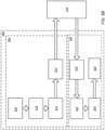
- the optical scanner 500 includes an optical transmitter 504 and an optical receiver 506.
- the optical transmitter 504 generally includes a light source 508, shaping or illumination optics 510 to illuminate a MEMS phased-array 512 with light from the light source, and imaging or projection optics 514 to transmit or project phase modulated light from the MEMS phased-array into a far field scene 516 to scan the far field scene in at least two dimensions.
- the light source 508 can include any type and number of light emitting devices capable of continuously emitting or pulsing a coherent light at a sufficient power level or power density, and at a single wavelength or frequency, or within a narrow range of wavelengths or frequencies, to enable light from the MEMS phased-array 512 to be modulated in phase and/or amplitude.
- the light source 508 is a continuous-wave light source that continuously emits a light that is modulated either in amplitude, for an AMCW LiDAR, or in frequency, for a FMCW LiDAR. Bcause objects in the far field scene are continuously illuminated; the light source can operate with less power compared to a high peak-power of pulsed systems.
- the light source 508 can include a number of lasers or laser emitters, such as diode lasers, vertical-cavity surface-emitting lasers (VCSELS).
- the light source the light source 508 includes a VCSEL array having a number of laser emitters to increase optical power while meeting or extending an eye-safe power limit.
- the light source 508 includes a number of high-power lasers producing from about 5000 to about 40,000 milliwatts (mW) of power at a wavelength ( ⁇ ) of from about 750 to about ⁇ 2000 nm.
- the illumination optics 510 can comprise a number of elements including lens integrators, mirrors and prisms, configured to transfer light from the light source 508 to the first MEMS phased-array 512 to illuminate a line of a specified width and covering substantially a full width and/or length of the MEMS phased-array.
- the illumination optics 510 include a microlens or lenticular array (described in greater detail below) to individually illuminate one or more modulators in the first MEMS phased-array 512.
- the projection optics 514 can also include lenses, integrators, mirrors and prisms, and are configured to transfer light from the MEMS phased-array 512 to illuminate a line or swath in the far field scene 516.
- the projection optics 514 includes magnifying optics or elements, such as Fourier Transform (FT) lenses and mirrors, to increase a field of view (FOV) of the optical scanner 500.
- the projection optics 514 include a lenticular array to disperse the light in a first direction to form the swath of illumination perpendicular to a direction over which the projected light is moved or steered in the far field scene 516.
- the optical receiver 506 generally includes receiving optics 518 to collect or receive light from the far field scene and direct or pass the received light onto a detector 520 or detector array.
- the receiving optics 518 can include lenses, integrators, mirrors and prisms, and are configured to receive and transfer light from the far field scene 516 to the onto the detector 520.
- the receiving optics 518 includes a lenticular array to increase an effective fill factor of the detector 520.
- the detector 520 can comprise any type of detector sensitive to light in the wavelengths generated by the light source 508, including a rolling shutter camera or cameras, a one or two dimensional array of photodiode detectors, or a single photon avalanche diode (SPAD) array.
- the receiving optics will be 2D, and the detector is a 2D array of detectors or a 2D detector array.
- LiDAR systems used in automobiles detector 520 can use lower density, higher sensitivity devices, such as APDs, for long range detection.
- the optical receiver 506 is a pointing optical receiver including a 2 nd MEMS phased-array 522 to de-scan collected or received light by selectively directing light reflected from a slice of the far field scene 516 onto the detector 520 while substantially rejecting background light.
- the 2 nd MEMS phased-array directs the light from the light source reflected from the far field scene 516 onto the detector 520 by adapting the direction to which it steers light based on information on the direction to which the 1 st MEMS phased-array 512 steers the light beam.
- the optical receiver 506 can further include detector optics 524 to transfer light from the 2 nd MEMS phased-array 522 on to the detector 520.
- the detector optics 524 can include lenses, integrators, mirrors and prisms, and configured to substantially fill or over fill the detector 520.
- the receiving optics 518 includes a lenticular array to increase an effective fill factor of a stacked phased-array 522.
- the optical receiver 506 is a pointing-receiver in which the 2 nd MEMS phased-array 522 selectively directs light reflected from a slice of far field scene 516 onto the 1D detector array while rejecting light reflected from the far field scene outside of the slice and background light.
- the optical scanner 500 includes an optical transmitter 504 and an optical receiver 506.
- the optical transmitter 504 additionally includes the light source 508 and illumination optics 510 to illuminate the 1 st MEMS phased-array 512 with light from the light source and projection optics 514 to transmit or project phase modulated light from the MEMS phased-array into the far field scene 516.
- the optical receiver 506 includes in addition to the 2 nd MEMS phased-array 522 the detector 520 and receiving optics 518 to collect or receive light from the far field scene 516 and to direct or pass the light to the 2 nd MEMS phased-array 522 and onto the detector 520.
- the 2 nd MEMS phased-array 522 directs the light from the light source reflected from the far field scene onto the detector 520, it is possible to reduce the size or width of the detector 520, compared to the case in which the 2 nd MEMS phased-array 522 is not provided. That is, because 2 nd MEMS phased-array 522 is capable of imaging a slice of the 2D scene 516 onto the detector 520, the detector can include a 1D array detector. The full scene is reconstructed by scanning the 2 nd MEMS phased-array.
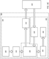
- the optical scanner 500 includes a shared MEMS phased-array 526 configured to modulate phases of the light from a light source 508 at a first time to scan a far field scene 516, and at a second time to de-scan collected or received light by directing light from the light source reflected from the far field scene onto a detector 520 while substantially rejecting background light.
- the optical scanner 500 includes an optical transmitter 504 and an optical receiver 506.
- the optical transmitter 504 includes in addition to the light source 508 and shared MEMS phased-array 526, illumination optics 510 to illuminate the MEMS phased-array with light from the light source and projection optics 514 to transmit or project phase modulated light from the MEMS phased-array into the far field scene 516.
- the optical receiver 506 includes in addition to the detector 520 and shared MEMS phased-array 526, receiving optics 518 to collect or receive light from the far field scene 516 and, optionally, detector optics 524 to direct or pass the light to the shared MEMS phased-array and onto the detector 520.
- the optical scanner 600 can include a MEMS phased-array 602 in an optical receiver 604 of the scanner, and a spatial light modulator (SLM 606) in an optical transmitter 608.
- the SLM 606 in the optical transmitter 608 need not include a solid state device, but can alternatively include a mechanical scanner, such as a spinning or moving mirror, to steer the light beam over a far field scene 610.
- the optical receiver 604 includes in addition to the MEMS phased-array 602 receiving optics 612 to collect or receive light from the far field scene 610 and to direct or pass the light to the MEMS phased-array and from there onto a detector 614.
- the optical transmitter 608 additionally includes a light source 616 and illumination optics 618 to illuminate the SLM 606 with light from the light source and projection optics 620 to transmit or project phase modulated light from the MEMS phased-array into the far field scene 610.
- Embodiments of a MEMS-based spatial light modulator (SLM) to form a MEMS phased-array suitable for use in an optical scanner will now be described.
- SLM spatial light modulator
- MEMS-based SLM suitable for use in a MEMS phased-array of a LIDAR system to modulate or steer a beam of light
- a ribbon-type SLM or ribbon MEMS phased-array including multiple electrostatically deflectable ribbons such as a Grating Light Valve (GLV TM ), commercially available from Silicon Light Machines, in Sunnyvale CA.
- Ribbon-type SLMs generally include a one dimensional (1D) linear array composed of thousands of free-standing, addressable electrostatically actuated movable structures, such as elongated elements or ribbons, each having a light reflective surface supported over a surface of a substrate.
- Each of the ribbons includes an electrode and is deflectable through a gap or cavity toward the substrate by electrostatic forces generated when a voltage is applied between the electrode in the ribbon and a base electrode formed in or on the substrate.
- the ribbon electrodes are driven by a drive channel in a driver, which may be integrally formed on the same substrate with the array.
- Ribbon-type SLMs are suited for a wide range of LiDAR applications because they are small, fast, low cost systems, which are simple to fabricate, integrate and package while still capable of providing large diffraction angles.
- ribbon-type SLMs are capable of working to produce 3D scans or models when used in combination with rolling shutter cameras, photodiode detector array and SPAD array, and a wide range of illumination sources, including a laser array or bar with multiple semiconductor diode lasers or VCSELs.
- FIGs. 7A and 7B An embodiment of a ribbon-type SLM will now be described with reference to FIGs. 7A and 7B .
- FIGs. 7A and 7B For purposes of clarity, many of the details of MEMS in general and MEMS-based SLMs in particular that are widely known and are not relevant to the present invention have been omitted from the following description.
- the drawings described are only schematic and are non-limiting. In the drawings, the size of some of the elements may be exaggerated and not drawn to scale for illustrative purposes. The dimensions and the relative dimensions may not correspond to actual reductions to practice of the invention.
- the SLM is a one dimensional (1D) ribbon-type SLM 700 that includes a linear array 702 composed of thousands of free-standing, addressable electrostatically actuated ribbons 704, each having a light reflective surface 706 supported over a surface of a substrate 708.
- Each of the ribbons 704 includes an electrode 710 and is deflectable through a gap or cavity 712 toward the substrate 708 by electrostatic forces generated when a voltage is applied between the electrode in the ribbon and a base electrode 714 formed in or on the substrate.
- the ribbon electrodes 710 are driven by a drive channel 716 in a driver 718, which may be integrally formed on the same substrate 708 with the linear array 702.
- FIG. 7B A schematic sectional side view of an elongated element or ribbon 704 of the SLM 700 of FIG. 7A is shown in FIG. 7B .
- the ribbon 704 includes an elastic mechanical layer 720 to support the ribbon above a surface 722 of the substrate 708, a conducting layer or electrode 710 and a reflective layer 724 including the reflective surface 706 overlying the mechanical layer and conducting layer.
- the mechanical layer 720 comprises a taut silicon-nitride film (SiNx), and is flexibly supported above the surface 722 of the substrate 708 by a number of posts or structures, typically also made of SiNx, at both ends of the ribbon 704.
- the conducting layer or electrode 710 can be formed over and in direct physical contact with the mechanical layer 720, as shown, or underneath the mechanical layer.
- the conducting layer or ribbon electrode 710 can include any suitable conducting or semiconducting material compatible with standard MEMS fabrication technologies.
- the electrode 710 can include a doped polycrystalline silicon (poly) layer, or a metal layer.
- the reflective layer 724 is metallic it may also serve as the electrode 710.
- the separate, discrete reflecting layer 724 can include any suitable metallic, dielectric or semiconducting material compatible with standard MEMS fabrication technologies, and capable of being patterned using standard lithographic techniques to form the reflective surface 706.
- a number of ribbons are grouped together to form a large number of MEMS pixels 726, with or more ribbons in the array driven by a single driver channel 716.
- FIG. 8 is a schematic representation of how the pitch and amplitude of an ensemble of SLM ribbons in FIGs. 7A and 7B can be adjusted to steer a beam of light.
- ribbons 804 are arranged in a "blaze" pattern 806 of pitch or period A. As the blaze pitch A is reduced, light is steered over larger angles ⁇ .
- the blaze period A can assume integer or non-integer values to allow continuous modulation of the steering angle ⁇ . The largest steering angle is achieved when the blaze period comprises two ribbons.
- FIG. 9 is a schematic representation of a portion of a linear array 902 in a ribbon-type SLM shown in cross-section to long axes of the ribbons.
- the deflection of ribbons 906 is varied to impart a monotonic phase variation along the array. Note that once the phase variation exceeds one wave (i.e. half wave deflection), the deflection pattern is continued via modulo division by the wavelength forming the blaze groupings 903.
- An SLM with programmable MEMS elements ribbons 906 allow light to be continuously scanned in angle, making it particularly useful in steering applications, such as LIDAR.
- FIG. 10 is a graph of intensity versus steering angle and illustrates the suitability of the ribbon-type SLM represented schematically in FIG. 9 for phased-array applications.
- the periodic spatial pattern along ribbon-type SLM shown in FIG. 9 creates a phased-array reflection, while varying the spatial period and amplitude of the pattern changes the reflected beam angle, allowing the ribbon-type SLM to rapidly cycle through patterns to sweep beam across field.
- a maximum intensity 1008 with which light is reflected from the array 902 shifts to the left as indicated by arrow 1010.
- the maximum intensity 1008 with which light is reflected from the array 902 shifts to the right as indicated by arrow 1012.
- the high switching speed of the ribbon-type SLM makes it attractive for MEMS phased-array applications such as LiDAR.
- designing a ribbon-type SLM for LiDAR presents two challenges.
- a large stroke i.e., an amount by which an individual ribbon can be deflected
- the ribbon-type SLM have a stroke up to or exceeding one-half the wavelength of the light being modulated or steered. For example, it has been found a stroke of approximately 0.8 ⁇ m is desirable to achieve adequate phase shift in applications for LIDAR using 1550 nm wavelengths.
- the stroke of the phase modulator scales linearly with the wavelength.
- a second challenge for ribbon-type SLMs used for MEMS phased-array is that the ribbons should include narrow ribbon widths to achieve wide angular swing.
- a ribbon used in ribbon-type SLMs for MEMS phased-array applications have a ribbon width of about ⁇ 5 ⁇ m or less, and in some embodiments can be as narrow as 0.5 ⁇ m.
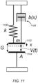
- FIG. 11 is a schematic diagram modeling a ribbon of ribbon-type SLM as a capacitor-on-a-spring.
- a voltage potential V(t) applied between a ribbon 1102 and a grounded lower or substrate electrode 1104 creates an electrostatic Coulomb attraction that deflects the ribbon a distance x towards the substrate electrode.
- the electrostatic force is balanced by an elastic restoring force (represented by a spring 1106 in FIG. 11 ).
- the elastic restoring force which is due to the taut silicon-nitride film the mechanical layer (shown as mechanical layer 720 in FIG.
- Reducing the squeeze film gap while maintaining or increasing the electrical gap can be done by inserting a dielectric between the ribbon and the substrate electrode.
- a solid dielectric film underneath the ribbon is used to improve damping (and heat transfer) in this way.
- the equivalent electrical thickness is G/ ⁇ r , where ⁇ r is the relative dielectric constant.
- ⁇ r is the relative dielectric constant.
- thick films i.e., films having a thickness greater than about 2 ⁇ m
- an existing MEMS process used to fabricate ribbon-type SLMs can be difficult or impractical, since intrinsic film stresses can cause such thick films to void or delaminate, and film roughness can become excessive with increased thickness. For this reason, a low dielectric constant material is frequently used.
- the squeeze film gap is reduced while maintaining or increasing the electrical gap by use of an electrically permeable damping structure formed over the substrate electrode during fabrication.
- the electrically permeable damping structure includes a dielectric layer suspended above and separated from the substrate electrode by a first gap or first air-gap, where the dielectric layer defines at least a top surface of the air-gap.
- this first gap is referred to as an air-gap, it need not be filled with air, but can alternatively be evacuated or filled with a mixture of other gases.
- the dielectric layer can substantially surround the air-gap to form a hermetic or hermetically sealed cavity.
- the first air gap is open to the MEMs environment, including a second gap or air-gap between the electrically permeable damping structure and a lower surface of the ribbons, and the entire environment of the ribbon-type SLM can be evacuated or filled with fill gases and hermetically sealed.
- Suitable fill gases can include pure form or mixtures of one or more of Nitrogen, Hydrogen, Helium, Argon, Krypton or Xenon.
- a ribbon-type SLM includes an electrically permeable damping structure to provide a large stroke while maintaining good damping, thereby enabling fast beam steering and large scan angles, and exceeding the wavelength of the light being modulated or steered to accommodate light having long wavelengths of up to about 10 ⁇ m.
- FIG. 12 is a sectional side view of a portion of the ribbon-type SLM of FIGs. 7A and 7B including such a damping structure.
- the ribbon-type SLM 1200 includes a bottom or lower electrode 1202 formed over a substrate 1204, and a static, electrically permeable damping structure formed over the bottom electrode.
- the electrically permeable damping structure includes a first air-gap 1206 and a dielectric layer 1208 suspended above and separated from the lower electrode 1202 by the first air-gap, and a second air-gap 1210 above the dielectric layer separating movable lengths of a plurality of ribbons 1212 of the ribbon-type SLM 1200 from the dielectric layer.
- a first air-gap 1206 and a dielectric layer 1208 suspended above and separated from the lower electrode 1202 by the first air-gap
- a second air-gap 1210 above the dielectric layer separating movable lengths of a plurality of ribbons 1212 of the ribbon-type SLM 1200 from the dielectric layer.
- each of the ribbons 1212 include a mechanical layer, typically formed from a taut layer of silicon nitride, and a ribbon or top electrode coupled through a bus 1214 to one of number of drive channels (not shown), and are configured to deflect towards the bottom electrode by electrostatic force generated between the top and bottom electrodes.
- the drive channels are integrally formed on the same substrate 1204 as the linear array of ribbons 1212.
- the device can further include a thin intermediate dielectric layer 1216, such as a silicon-dioxide between the substrate 1204 and the lower electrode 1202 to electrically insulate the lower electrode.
- a thin intermediate dielectric layer 1216 such as a silicon-dioxide between the substrate 1204 and the lower electrode 1202 to electrically insulate the lower electrode.
- the ribbons 1212 are independently deflectable towards the bottom electrode 1202 by a distance substantially equal to a thickness of the second air-gap 1210.
- the thickness of the second air-gap 1210 is ⁇ G/3
- the thickness of the first air-gap 1206 is ⁇ 2G/3, where G is a distance between the bottom electrode 1202 and the ribbons 1212 in an undeflected or quiescent state.
- an electrically permeable damping structure such as described above and having a first air gap 1206 of about 2.5 ⁇ m and a second air-gap 1210 up to about 1.5 ⁇ m, improves settling time, while maintaining a high switching speed and substantially preventing pull-in or snap-down of the ribbons 1212.
- the ratio of second air-gap thickness to first air-gap thickness can be decreased to accommodate narrower ribbons which require stronger damping.
- the MEMS phased-array 1300 can include multiple ribbon-type SLMs 1302a, 1302b, each with a one dimensional (1D) array 1304a, 1304b, arranged in a line along a common or shared long axis 1306 and operated to increase an area over which modulated light can be scanned, and stacked to increase an axial dimension parallel to the long axis of the arrays.
- each of the arrays 1304a, 1304b includes hundreds or thousands of free-standing, addressable electrostatically actuated ribbons 1308a, 1308b.
- the ribbon-type SLM 700 described above with respect to FIGs.
- each of the ribbons 1308a, 1308b has a light reflective surface, includes an electrode and is deflectable through a gap or cavity toward a substrate 1310 by electrostatic forces generated when a voltage is applied between the electrode in the ribbon and a base electrode in the substrate.
- Each of the ribbons 1308a, 1308b is driven by a drive channel 1312a, 1312b in a driver 1314a, 1314b, which may be integrally formed on the same substrate 1310 with the arrays 1304a, 1304b.
- each of the ribbon-type SLMs 1302a, 1302b including the arrays 1304a, 1304b and drivers 1314a, 1314b, are integrally formed on a single, shared substrate 1310.
- each of the ribbon-type SLMs 1302a, 1302b can be integrally formed on separate substrates, which are then packaged in a single, share integrated circuit (IC) package.
- IC integrated circuit
- each of the ribbon-type SLMs 1302a, 1302b are separately packaged and then mounted to a single, shared printed circuit board (PCB).
- PCB printed circuit board
- the MEMS phased-array can include multiple ribbon-type SLMs or a single ribbon-type SLM having multiple one dimensional (1D) arrays arranged and operated in parallel to increase the active aperture of the optical scanner.
- Increasing the functional area of the MEMS phased-array in this manner allows for simpler optics, enables an increased field of view (FOV) and system point spread resolution, as well as increased sensitivity by collecting more light in de-scan operations.
- FOV field of view
- FIG. 14 is a diagram illustrating a top view of an embodiment of a MEMS phased-array 1400 including multiple ribbon-type SLMs 1402A and 1402B each including an array 1404 of a plurality of ribbons 1406 arranged in parallel.
- the ribbon-type SLM 1402A and 1402B are integrally formed on a shared substrate 1408, and the ribbons 1406 are driven by drive channels 1416 in drivers 1418, which may be integrally formed on the same substrate 1408 with the arrays 1404.
- all of the multiple ribbon-type SLMs 1402A and 1402B can be driven by a single shared driver 1418.
- FIGs. 15A through 15C are diagrams illustrating another embodiment of a MEMS phased-array 1500 including a single ribbon-type SLM 1502 in which each of the ribbons 1504 of the SLM are divided by posts 1506 along a long axis thereof to form a plurality of parallel 1D arrays 1508a, 1508b, and 1508c. Although only three parallel 1D arrays 1508a, 1508b, 1508c are shown it will be understood that the ribbon-type SLM 1502 can be divided into any number of parallel 1D arrays from 2 to over 50.
- a schematic sectional side view of a movable ribbons 1504 of the SLM 1502 of FIG. 15A in an undeflected or quiescent state is shown in FIG. 15B .
- FIG. 15C A schematic sectional side view of a movable ribbons 1504 of the SLM 1502 of FIG. 15A in a deflected or active state is shown in FIG. 15C .
- the ribbon 1504 includes an elastic mechanical layer 1510 to support the ribbon above a bottom electrode 1512 formed on a surface of a substrate 1514, a ribbon or top electrode 1516 and a reflective layer 1518 including a light reflective surface overlying the mechanical layer or top electrode.
- the SLM 1502 further includes a number of drive channels 1520 in a driver 1522 integrally formed on the same substrate 1514 as the linear 1D arrays 1508a, 1508b, and 1508c.
- the MEMS phased-array includes a blazed grating ribbon-type or ribbon MEMS array, in which each elongated element or ribbon of a ribbon-type SLM has a reflective surface with a blazed profile.
- a blazed profile it is meant wherein each of the ribbons have a reflective surface across a width of the ribbon that is angled at the blaze angle relative to a surface of the SLM or surface of a substrate on which the SLM is fabricated.
- the reflective surfaces have a stepped profile to produce an effective blaze at a blaze angle.
- the blaze angle on the ribbon adjusts a power and contrast in modulated light from the SLM in the zeroth (0 th ) and higher orders, providing higher contrast in the 0 th order, and higher contrast and/or power in the first (1 st ) and higher orders.
- For scanning operation using a blazed ribbon in conjunction with the blazed operation or method described above with respect to FIGs. 8 through 10 , shifts a center of a "scan envelope" (angles between +/- first orders in an SLM with flat ribbons) towards the first order, and away from the zeroth (0 th ) and order or incidence angle.
- FIG. 16A illustrate a cross-sectional view of a single elongated element or ribbon 1602 having a stepped profile to produce an effective blaze surface 1604 at a blaze angle ⁇ at a blaze angle.
- the ribbon 1602 generally includes a rectangular body 1606 and a stepped reflector 1608.
- the rectangular body 1606 can include silicon nitride and the stepped reflector 1608 can include an optically reflective material such as aluminum.
- the stepped reflector 1608 forms first and second surfaces, 1610 and 1612, of the ribbon 1602.
- the first and second surfaces, 1610 and 1612, are generally separated by a height difference of an eighth wavelength ⁇ /8 of an incident light to form a blaze profile 1614.
- FIG. 16B A first cross-sectional view of a portion of a blazed ribbon-type or ribbon MEMS phased-array 1616 in a non-activated state with the ribbons 1602 on a grating pitch A and with the first surfaces 1610 defining a grating plane 1618 is illustrated in FIG. 16B .
- the incident light (I) of wavelength ⁇ illuminates the blazed ribbon MEMS phased-array 1616 at an angle normal to the grating plane 1618, and diffracts light into a number of diffraction orders D 0 , D -1 and D 1 based on a profile of the blazed ribbons 1602.
- the zeroth order diffraction, D 0 is normal to the grating plane 1618.
- ⁇ 1 arcsin ( ⁇ /A)
- A is the grating pitch of the first and second surfaces, 1610, 1612, of the ribbons 1602.
- the diffraction angle ⁇ 1 is approximately four times the blaze angle y, or less than about 15°.
- FIG. 16C A second cross-sectional view of the blazed ribbon MEMS phased-array 1616 in an activated state in which the ribbons 1602 are moved towards a substrate 1622 by applying an electrical bias between the ribbons and the bottom electrode 1620 is illustrated in FIG. 16C .
- the blazed ribbon MEMS phased-array 1616 is operated using a blazed operation or method similar to that described above with respect to FIGs. 8 through 10 .
- ribbons 1602 having a blaze profile 1614 are arranged in a "blaze" pattern 1624 of pitch or period A.
- the blaze period A can assume integer or non-integer values to allow continuous modulation of the steering angle ⁇ 3 .
- the blaze pitch A is reduced, light is steered over larger angles from ⁇ 1 to ⁇ 3 .
- FIG. 17 is an optics diagram illustrating illumination optics 1702 and projection optics 1704 for an optical scanner including a number of MEMS phased-arrays 1706 to steer light 1708 to scan a far field scene 1710.
- the illumination optics 1702 can include a lenticular array or an array of microcylinder lenses 1712 to form individual columns of light from a coherent light source, and an imaging lens 1716 to focus the collimated light onto individual modulators of the MEMS phased-array 1706.
- the light coherent light source includes an array of light emitting devices such as VCSEL lasers 1718.
- the illumination optics 1702 and projection optics 1704 can achieve greater than 5 watts (W) peak power with 10 nanosecond (ns) pulse, at a repetition rate of up to 1 MHz, while each beam of light projected into the far field scene has an average power less than about 2.5 microwatts (mW) and thus is eye safe.
- W watts
- ns nanosecond
- mW microwatts
- the projection optics 1704 can include one or more lenses, such as a Fourier lens 1720 and a fish-eye lens to spread the light from the MEMS phased-array to the far field scene in at least an angular dimension, transverse to an axial dimension over which light is scanned by phase modulation of the MEMS phased-array 1706.
- a Fourier lens 1720 and a fish-eye lens to spread the light from the MEMS phased-array to the far field scene in at least an angular dimension, transverse to an axial dimension over which light is scanned by phase modulation of the MEMS phased-array 1706.
- the illumination optics 1702 and projection optics 1704 can achieve greater than 5 watts (W) peak power with 10 nanosecond (ns) pulse, at a repetition rate of up to 1 MHz, while each beam of light projected into the far field scene has an average power less than about 2.5 microwatts (mW) and thus is Class 1, eye safe.
- W watts
- ns nanosecond
- mW microwatts
- the MEMS phased-array 1706 having an individual element size 4.25 ⁇ m with an enclosure aperture of 3mm the MEMS phased-array is capable of providing a FOV of 25.5 degrees, with over 1000 resolvable lines.
- At least one of the illumination optics or the projection optics or receiving optics includes anamorphic optics for focusing light from a light source onto a MEMS phased-array, and/or focusing modulated light from the MEMS phased-array into the far field scene.
- Anamorphic optics are desirable to provide a vertical or transverse numerical aperture (NA) along a vertical axis of the MEMS phased-array, transverse to the direction over which the light is scanned, that is smaller than a diffraction angle of the modulated light reflected from the array along a vertical or transverse axis of the scan direction, and a horizontal or longitudinal NA along the horizontal or longitudinal axis of the array that is greater than the vertical or transverse NA, as the field of view and resolution requirement for the vertical and horizontal axis may differ.
- the horizontal axis optics will match the FOV of the phased-array device to the requirements of the horizontal scan of the system, while the FOV of the vertical scan is determined by the vertical numerical aperture as set by the illuminating or detector array system.
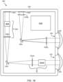
- FIG. 18A and 18B are an optics diagram illustrating both top and side views of light paths for anamorphic illumination and imaging optics according to an embodiment of the present disclosure.
- the top view shows an optical paths along a pixel arranged direction.
- the light path begins at a light source, such as a laser 1802 shown, in this embodiment, as including a plurality of light emitting or laser diodes 1804 arranged as a bar laser to illuminate a substantially linear portion of a 1D or 2D array 1806 of an SLM through anamorphic illumination optics 1807, including a first optical element or lens 1808 and second optical element or lens 1810.
- the anamorphic illumination optics 1807 are depicted or represented by two single lenses 1808 and 1810, it will be appreciated that the anamorphic illumination optics can include any number of prisms, lenses and to refract and transmit light from the laser 1802 to the linear array 1806 to fully illuminate the linear array.
- the lens 1808 is usually called FAC lens (Fast Axis Collimator) to collimate laser from the emitters along the vertical axis or fast axis of emitters.
- the laser 1802 is a bar laser including multiple semiconductor diode lasers or emitter arranged along common long axis. Each emitter of the bar laser works as spatially single mode laser and it has Gaussian beam profile along the vertical axis.
- a light pipe or a fly eye lens array can be included in the optical element or lens 1810 to homogenize the light from the light emitting or laser diodes 1804 of the bar laser.
- a bar laser has multiple emitters and generally has 10 mm width along the horizontal axis, it functions to some degree as a NA.
- the NA would be D/2f, where D is size of the bar laser and f is the focal length of the cylindrical lens in the optical element or lens 1810.
- the NA number would be extended.
- NA along the fast axis or vertical axis is low, NA along the slow axis or horizontal axis could be much bigger than the fast axis.
- the pixel arranged direction of the linear array 1806 is set parallel to emitter arranged direction of the bar laser 1802. Such the configuration enables to use diffraction beams effectively.
- the NA of illumination optics has some number because of the size of emitter array, while the condition to separate diffraction beams by the linear array 1806 is limited.
- the imaging optics 1812 can include magnification elements, such as a Fourier Transform (FT) lens 1816, and Fourier aperture 1818.
- FT Fourier Transform
- the array includes just one or a few pixels along the horizontal direction and 1 st order beams can be separated from 0 th order beam only when the illumination NA is almost zero.
- the dashed lines illustrate 1 st order beams while the solid, bold line show the main, 0 th order beams. Since the NA of illumination beam is kept after it is diffracted to 1 st order beam by the linear array 1806, some of the 1 st order beams pass through the Fourier aperture 1818. On the other hand, NA of illumination optics along the vertical axis is small and the number of modulators in a single pixel is so large that diffraction, main beams are separated.
- Modulated light from the linear array 1806 is then transmitted through imaging optics 1812 to the imaging plane 1814.
- the imaging optics 1812 can also include anamorphic optics, represented here by anamorphic lens 1820 and microlens or lenticular array 1822. This embodiment is particularly advantageous where the pixel size of array 1806 is not square.
- FIG. 18B shows that 0 th order beam and diffracted +/- 1 st order beams on the Fourier aperture 1818.
- ellipse 1824 represents the 0 th order beam
- ellipse 1826 represent 1 st order beams along the vertical direction
- ellipse 1828 represent 1 st order beams along the horizontal direction.
- the aperture size along the vertical axis (vertical NA 1830) is equivalent to the diffraction angle of 1 st order beam and a size of the 0 th order beam (represented by ellipse 1824) along the horizontal axis is the same as the horizontal NA 1832 of illumination optics (lenses 1808 and 1810 in FIG 18A ).
- the illumination and imaging optics of the embodiment of FIG. 18A is suitable for use in a LiDAR system, such as that shown in FIGs. 1 and 3 .
- the power of bar lasers including a plurality of laser diodes is not as high as in the examples given above, and is generally equal to or less than 100 watts (W).
- W watts
- multiple bar lasers should be used.
- a vertical stack of bar lasers can be used to achieve higher powers.
- FIG. 19 is a schematic block diagram of a compact optical scanner 1902 shown in a cut-away view, and including one or more MEMS phased-arrays 1904, 1906, and illustrating folded light paths for illuminating the MEMS phased-arrays, projecting modulate light therefrom, and receiving and de-scanning light onto a detector 1908.
- the folded light paths enable a compact optical scanner 1902 size, for example of about 7 cm by 7cm with a thickness of about 2cm, or about the size of a deck of cards.
- the optical scanner 1902 includes a housing or enclosure 1910, and one or more openings or apertures 1912, 1914, through which light can be projected to scan a far field scene (not shown in this figure) and received back from the far field scene.
- the apertures 1912, 1914 are covered or sealed by lenses 1916, 1918, to further magnify or expand the projected light, to focus the received light, and/or to provide an environmentally sealed enclosure 1910 for the optical scanner 1902.
- the lenses 1916, 1918 can include fish-eye lenses to further increase a field of view (FOV) of the optical scanner 1902.
- FOV field of view
- the optical scanner 1902 further includes illumination optics 1920 to direct light from a coherent light source 1922 on to the MEMS phased-array 1904, imaging or projection optics 1924 to transmit or project phase modulated light from the MEMS phased-array into the far field scene, and receiving optics 1926 to receive and direct light from the far field scene onto the detector 1908.
- the light source 1922 can include any type and number of light emitting devices, such as lasers, diode lasers or VCSELS.
- the illumination optics 1920 can comprise a number of elements including one or more lenses 1920a, and integrators, mirrors or prisms 1920b, configured to transfer light from the light source 1922 to the MEMS phased-array 1904 to illuminate a line of a specified width and covering substantially a full width length of the MEMS phased-array.
- the projection optics 1924 can also include lenses 1924a, and integrators, mirrors or prisms 1924b, configured to transfer light from the MEMS phased-array 1904 to illuminate a line or swath in the far field scene.
- the receiving optics 1926 can include one or more lenses 1926a, 1926b, integrators, mirrors and/or prisms configured to receive and transfer light from the far field scene to the onto the detector 1908.
- the detector 1908 can comprise any type of detector sensitive to coherent light in the wavelengths generated by the light source 1922, including a rolling shutter camera or cameras, a one or two dimensional array of photodiode detectors, or a SPAD array.
- the enclosure 1910 of the optical scanner 1902 can further include or house electronic circuits 1928 necessary for the operation of the optical scanner, such as a controller, power supplies for the controller, light source 1922, MEMS phased-arrays 1904, 1906, and detector 1908, one or more memories and interfaces to a host system.
- electronic circuits 1928 necessary for the operation of the optical scanner, such as a controller, power supplies for the controller, light source 1922, MEMS phased-arrays 1904, 1906, and detector 1908, one or more memories and interfaces to a host system.
- one or more of the illumination optics 510, projection optics 514, receiving optics 518, and detector optics 524 can include a microlens or lenticular array.
- illumination optics in the transmitter including a lenticular array is useful in conjunction with a light source including a VCSEL array, as shown in FIG. 17 , to provide independent optical channels.
- a lenticular optical array is also particularly useful distribute light on the multiple ribbon MEMS phased-arrays, either in the optical transmitter or receiver, such as those shown in FIGs. 13 through 15 , to distribute light on the multiple arrays, and/or in projection optics to disperse to form the swath of illumination in the far field scene.
- a lenticular array is useful in receiver array optics to increase an effective fill factor of the receiver array.
- FIG. 20A is a schematic block diagram illustrating a top view of an embodiment of a lenticular array
- FIG. 20B is a cross sectional view of the lenticular array of FIG. 20A
- FIG. 20B illustrates 0th order illumination of a single modulator in a ribbon MEMS phased-array by single element of the lenticular array of FIG. 20A
- the lenticular array 2000 includes a molded surface forming multiple individual lenses or elements, such as micro-lenses or cylindrical lenses, configured to concentrate, either focus or project, light more in one direction than in another.
- the lenticular array 2000 is adapted or configured to focus light onto individual ribbons or portions of ribbons divided by posts in a ribbon MEMS phased-array 2002, and the individual lenses or elements include cylindrical lenses 2004, each having a long axis parallel to a long axis 2006 of one or more ribbon MEMS phased-array arranged either stacked as shown in FIG. 13 or arranged in parallel as shown in FIGs. 14 and 15 , and perpendicular to a long axis 2008 of the ribbons.
- the cylindrical lenses 2004 focus or concentrate incoming light 2010 on a center of each individual ribbon or portion of a divided ribbon in the ribbon MEMS phased-array 2002.
- a lenticular array 2000 to carefully shape or focus illumination onto a central portion of the ribbons of the ribbon MEMS phased-array, or to collimate and project only light modulated from the central portion of the ribbons.
- a rule of thumb is that a width of sweet-spot 2014 should be roughly on the order of 1/10 th to 1/3 rd the length the ribbon 2012, depending on the contrast ratio.
- the individual lenses or elements enable only a 0 th order of light 2016 to focused on or modulated by the sweet-spot 2014 while rejecting other orders of light 2018, thereby increasing contrast and resolution of the optical scanner.
- a method of operating an optical scanner including a first microelectromechanical system (MEMS) phased-array for use in a light detection and ranging (LiDAR) system will now be described with reference to the flow chart of FIG. 21 .
- the method begins with illuminating a first MEMS phased-array with light from a coherent light source (2102).
- the first MEMS phased-array is controlled to modulate phases of the light from the coherent light source and project the modulated light from the first MEMS phased-array to a far field scene (2104), and the first MEMS phased-array is further operated or controlled to scan the far field scene (2106).
- the first MEMS phased-array is adapted or configured to scan the far field scene in two-dimensions (2D), including an angular dimension and an axial dimension parallel to a long axis of the first MEMS phased-array.
- 2D two-dimensions
- the second MEMS phased-array is controlled to de-scan the received light by directing substantially only light originating from the coherent light source and reflected from the far field scene onto a detector while rejecting background light (2110).
- the first MEMS phased-array and the second MEMS phased-array are the same, shared MEMS phased-array
- controlling the first MEMS phased-array includes controlling the shared MEMS phased-array at a first time to modulate phases of the light from the coherent light source to scan the far field scene in 2D
- controlling the second MEMS phased-array includes controlling the shared MEMS phased-array at a second time to de-scan the received light by directing light from the coherent light source reflected from the far field scene onto the detector and rejecting background light.
Landscapes
- Engineering & Computer Science (AREA)
- Physics & Mathematics (AREA)
- General Physics & Mathematics (AREA)
- Microelectronics & Electronic Packaging (AREA)
- Radar, Positioning & Navigation (AREA)
- Computer Networks & Wireless Communication (AREA)
- Remote Sensing (AREA)
- Optics & Photonics (AREA)
- Computer Hardware Design (AREA)
- Electromagnetism (AREA)
- Optical Radar Systems And Details Thereof (AREA)
- Mechanical Optical Scanning Systems (AREA)
- Mechanical Light Control Or Optical Switches (AREA)
Claims (19)
- Optischer Scanner (500), umfassend:einen optischen Transmitter (504) zum Empfangen von Licht von einer Lichtquelle (508) und zum Modulieren von Phasen von mindestens einem Teil des empfangenen Lichts, um Licht auf eine Fernfeldszene (516) in zwei Dimensionen zu projizieren, wobei die zwei Dimensionen eine erste Richtung, über die das Licht gestreut wird, um einen Beleuchtungsstreifen zu bilden, und eine zweite Dimension umfassen, über die der Streifen durch Modulieren von Phasen des von der Lichtquelle (508) empfangenen Lichts gesteuert wird; undeinen optischen Empfänger (506), der eine Anzahl von ersten mikroelektromechanischen System (MEMS) Phased-Arrays (512) umfasst, die jeweils ein Band-MEMS-Phased-Array mit einer parallelen Anordnung von lichtreflektierenden Bändern umfassen, um Licht von der Fernfeldszene zu empfangen und zumindest einen Teil des empfangenen Lichts auf einen Detektor (520) zu richten,wobei die Anzahl der ersten MEMS-Phased-Arrays (512) eingerichtet ist, das empfangene Licht abzutasten, indem sie Licht von der Lichtquelle (508), das von der Fernfeldszene (516) reflektiert wird, auf den Detektor (520) lenken, während sie Hintergrundlicht (2110) zurückweisen,wobei der optische Empfänger (506) ferner eine Empfangsoptik (518) umfasst, um Licht von der Fernfeldszene (516) zu empfangen und empfangenes Licht auf die Anzahl der ersten MEMS-Phased-Arrays (512) zu richten, und wobei die Empfangsoptik (518) eine linsenförmige Anordnung umfasst, um einen effektiven Füllfaktor der Anzahl der ersten MEMS-Phased-Arrays (512) zu erhöhen.
- Optischer Scanner (500) nach Anspruch 1, wobei der optische Transmitter (504) eine Anzahl von zweiten MEMS-Phased-Arrays umfasst, um Licht von der Lichtquelle (508) zu empfangen und die Phasen von mindestens einem Teil des empfangenen Lichts zu modulieren, um Licht zweidimensional auf die Fernfeldszene (516) zu projizieren.
- Optischer Scanner (500) nach Anspruch 2, wobei der optische Transmitter (504) ferner eine Projektionsoptik (514) umfasst, um Licht von der Anzahl der zweiten MEMS-Phased-Arrays auf die Fernfeldszene (516) zu projizieren, und wobei die Projektionsoptik (514) ein linsenförmiges Array umfasst, um das Licht in der ersten Richtung zu streuen, um den Beleuchtungsstreifen zu bilden, und ein Sichtfeld (FOV) des optischen Scanners (500) zu vergrößern.
- Optischer Scanner (500) nach Anspruch 3, wobei die Lichtquelle (508) ein Oberflächenemittierender Laser mit vertikalem Resonator (VCSEL)-Array mit einer Vielzahl von Emittern umfasst, um die optische Leistung zu erhöhen und eine augensichere Leistungsgrenze zu erweitern.
- Optischer Scanner (500) nach Anspruch 4, wobei der optische Transmitter (504) ferner eine Beleuchtungsoptik umfasst, um die Anzahl der zweiten MEMS-Phased-Arrays mit Licht von der Lichtquelle (508) zu beleuchten, und wobei die Beleuchtungsoptik eine linsenförmige Anordnung umfasst, um einen oder mehrere Lichtmodulatoren in der Anzahl der zweiten MEMS-Phased-Arrays individuell zu beleuchten.
- Optischer Scanner (500) nach Anspruch 1, wobei der Detektor (520) ein eindimensionales (1D) Detektorarray umfasst und der optische Empfänger (506) ein Punkt-Empfänger ist, bei dem die ersten MEMS-Phased-Arrays (512) selektiv Licht, das von einer Scheibe der Fernfeldszene (516) reflektiert wird, auf das 1D-Detektorarray lenken, während sie Licht, das von der Fernfeldszene (516) außerhalb der Scheibe reflektiert wird, und Hintergrundlicht (2110) zurückweisen.
- Optischer Scanner (500) nach Anspruch 1, wobei das Band-MEMS-Phased-Array eine Vielzahl von Bändern umfasst, die in parallelen Reihen über einem Substrat aufgehängt sind, wobei jedes Band eine lichtreflektierende Oberfläche und eine Länge senkrecht zu einer Längsachse des Band-MEMS-Phased-Arrays aufweist, und wobei das Band-MEMS-Phased-Array eingerichtet ist, mindestens eine Anzahl der mehreren Bänder in Richtung des Substrats abzulenken, um die Phasen des davon reflektierten Lichts zu modulieren, um die Fernfeldszene (516) in einer Winkeldimension und einer axialen Dimension parallel zu der langen Achse des Phased-Arrays abzutasten.
- Optischer Scanner (500) nach Anspruch 7, wobei die Anzahl der ersten MEMS-Phased-Arrays (512) mehrere Band-MEMS-Phased-Arrays umfasst, die in Reihe angeordnet sind, um eine aktive Apertur des optischen Scanners (500) zu vergrößern.
- Optischer Scanner (500) nach Anspruch 8, wobei das Band-MEMS-Phased-Array ferner Dämpfungsstrukturen zwischen der Vielzahl von Bändern und dem Substrat umfasst, um die Modulation von Lichtphasen mit langen Wellenlängen zu ermöglichen.
- Optischer Scanner (500) nach Anspruch 7, wobei jedes der Vielzahl von Bändern durch Pfosten entlang seiner Länge geteilt ist, um eine Vielzahl von parallel angeordneten Band-MEMS-Phased-Arrays zu bilden, um eine aktive Apertur des optischen Scanners (500) zu vergrößern.
- Optischer Scanner (500) nach Anspruch 7, wobei das Band-MEMS-Phased-Array Bänder umfasst, die ein Blaze-Profil aufweisen, um eine0-te Ordnung des von dem Band-MEMS-Phased-Array reflektierten Lichts zu verschieben.
- Optischer Scanner (500), umfassend:einen optischen Transmitter (504), der eine Anzahl von ersten mikroelektromechanischen System (MEMS) Phased-Arrays (512) umfasst, um Licht von einer Lichtquelle zu empfangen und Licht auf eine Fernfeldszene (516) in zwei Dimensionen zu projizieren, wobei die zwei Dimensionen eine erste Richtung, über die das Licht gestreut wird, um einen Beleuchtungsstreifen zu bilden, und eine zweite Dimension, über die der Streifen durch Modulieren von Phasen von mindestens einem Teil des von der Lichtquelle (508) empfangenen Lichts gesteuert wird, umfassen; undeinen optischen Empfänger (506), um Licht zu empfangen, das zumindest einen Teil des Lichts vom optischen Sender (504) umfasst, das von der Fernfeldszene (516) reflektiert wird, und um zumindest einen Teil des empfangenen Lichts auf einen Detektor (520) zu richten,wobei der optische Empfänger (506) umfassteine Anzahl von zweiten mikroelektromechanischen System (MEMS) Phased-Arrays, von denen jedes ein Band-MEMS-Phased-Array mit einer parallelen Anordnung von lichtreflektierenden Bändern umfasst, undeine Empfangsoptik (518) zum Empfangen von Licht von der Fernfeldszene (516) und zum Richten des empfangenen Lichts auf die MEMS-Phased-Arrays, die eine linsenförmige Anordnung umfassen, um einen effektiven Füllfaktor der MEMS-Phased-Arrays zu erhöhen.
- Optischer Scanner (500) nach Anspruch 12, wobei die Anzahl der ersten MEMS-Phased-Arrays (512) ein Band-MEMS-Phased-Array umfasst, das eine Vielzahl von Bändern umfasst, die in parallelen Reihen über einem Substrat aufgehängt sind, wobei jedes Band eine lichtreflektierende Oberfläche und eine Länge senkrecht zu einer Längsachse des Band-MEMS-Phased-Arrays aufweist, und wobei das Band-MEMS-Phased-Array eingerichtet ist, mindestens eine Anzahl der Vielzahl von Bändern in Richtung des Substrats abzulenken, um die Phasen des von der Lichtquelle empfangenen Lichts zu modulieren, um Licht auf die Fernfeldszene (516) in einer Winkeldimension und einer axialen Dimension parallel zur Längsachse des Band-MEMS-Phased-Arrays zu projizieren.
- Optischer Scanner (500) nach Anspruch 13, wobei das Band-MEMS-Phased-Array Bänder mit einem Blaze-Profil umfasst.
- Optischer Scanner (1902), umfassend:ein mikroelektromechanisches System (MEMS) Phased-Array, das jeweils ein Band-MEMS-Phased-Array mit einer parallelen Anordnung von lichtreflektierenden Bändern umfasst;eine kohärente Lichtquelle (1922);eine Beleuchtungsoptik (1920), um das MEMS-Phased-Array (1904) mit Licht von der kohärenten Lichtquelle (1922) zu beleuchten;eine Projektionsoptik (1924) zur Projektion von Licht aus dem MEMS-Phased-Array auf eine Fernfeldszene;eine Empfangsoptik (1926) zum Empfangen von Licht aus der Fernfeldszene und zum Richten des empfangenen Lichts auf das MEMS-Phased-Array (1904), das ein linsenförmiges Array (2000) umfasst, um einen effektiven Füllfaktor des Band-MEMS-Phased-Arrays zu erhöhen; undeinen Detektor (1908), auf den das MEMS-Phased-Array (1904) zumindest einen Teil des empfangenen Lichts lenkt,wobei das MEMS-Phased-Array (1904) eingerichtet ist:zu einem ersten Zeitpunkt die Phasen des Lichts von der kohärenten Lichtquelle (1922) modulieren, um Licht auf die Fernfeldszene in zwei Dimensionen (2D) zu projizieren, undzu einem zweiten Zeitpunkt das empfangene Licht zu de-scannen, indem Licht von der kohärenten Lichtquelle (1922), das von der Fernfeldszene reflektiert wird, auf den Detektor gerichtet wird und Hintergrundlicht (2110) zurückgewiesen wird.
- Optischer Scanner (1902) nach Anspruch 15, wobei das Band-MEMS-Phased-Array eine Vielzahl von Bändern umfasst, die in parallelen Reihen über einem Substrat aufgehängt sind, wobei jedes Band eine lichtreflektierende Oberfläche und eine Länge senkrecht zu einer Längsachse des Band-MEMS-Phased-Arrays aufweist, und wobei das Band-MEMS-Phased-Array eingerichtet ist, mindestens eine Anzahl der Vielzahl von Bändern in Richtung des Substrats abzulenken, um die Phasen des davon reflektierten Lichts zu modulieren, um Licht auf die Fernfeldszene in einer Winkeldimension und einer axialen Dimension parallel zur Längsachse des Band-MEMS-Phased-Arrays zu projizieren.
- Optischer Scanner (1902) nach Anspruch 16, wobei das Band-MEMS-Phased-Array (1904) mehrere parallel angeordnete Band-Phased-Arrays umfasst, um eine aktive Apertur des Systems zu vergrößern.
- Optischer Scanner (1902) nach Anspruch 16, wobei jedes der Vielzahl von Bändern durch Pfosten entlang seiner Länge geteilt ist, um mehrere parallel angeordnete MEMS-Phased-Arrays von Bändern zu bilden, um eine aktive Apertur des Systems zu vergrößern.
- Optischer Scanner (1902) nach Anspruch 15, wobei mindestens eine der Beleuchtungsoptiken (1920), Projektionsoptiken (1924) oder Empfangsoptiken (1926) eine gefaltete anamorphotische Optik umfasst.
Applications Claiming Priority (4)
| Application Number | Priority Date | Filing Date | Title |
|---|---|---|---|
| US201962891977P | 2019-08-27 | 2019-08-27 | |
| US201962947514P | 2019-12-12 | 2019-12-12 | |
| US17/001,477 US12117606B2 (en) | 2019-08-27 | 2020-08-24 | MEMs phased-array for LiDAR applications |
| PCT/US2020/048179 WO2021041660A1 (en) | 2019-08-27 | 2020-08-27 | Mems phased-array for lidar applications |
Publications (3)
| Publication Number | Publication Date |
|---|---|
| EP4022345A1 EP4022345A1 (de) | 2022-07-06 |
| EP4022345A4 EP4022345A4 (de) | 2023-09-06 |
| EP4022345B1 true EP4022345B1 (de) | 2025-05-14 |
Family
ID=74685213
Family Applications (1)
| Application Number | Title | Priority Date | Filing Date |
|---|---|---|---|
| EP20858593.5A Active EP4022345B1 (de) | 2019-08-27 | 2020-08-27 | Mems-phased-array für lidar-anwendungen |
Country Status (7)
| Country | Link |
|---|---|
| US (1) | US12117606B2 (de) |
| EP (1) | EP4022345B1 (de) |
| JP (1) | JP7589234B2 (de) |
| KR (1) | KR102783413B1 (de) |
| CN (1) | CN114631036B (de) |
| TW (1) | TWI883034B (de) |
| WO (1) | WO2021041660A1 (de) |
Families Citing this family (17)
| Publication number | Priority date | Publication date | Assignee | Title |
|---|---|---|---|---|
| MX2021016073A (es) * | 2019-12-31 | 2022-03-25 | Illumina Inc | Funcionalidad de enfoque automático en el análisis óptico de muestras. |
| US12405534B2 (en) * | 2021-02-05 | 2025-09-02 | Silicon Light Machines Corporation | MEMs based spatial light modulators with improved thermal control |
| US12436242B2 (en) | 2021-02-12 | 2025-10-07 | Silicon Light Machines Corporation | High contrast MEMS phased-array |
| CN115079201A (zh) * | 2021-03-10 | 2022-09-20 | 中强光电股份有限公司 | 光学扫描系统 |
| JP2024510124A (ja) * | 2021-03-17 | 2024-03-06 | ニューラル プロパルション システムズ,インコーポレイテッド | 複数の光学部品アレイを結合するためのシステム、方法、及びデバイス |
| CN113075685B (zh) * | 2021-05-07 | 2024-01-12 | 万航星空科技发展有限公司 | 一种基于无人机的机载激光雷达系统 |
| US11958738B2 (en) * | 2021-07-26 | 2024-04-16 | Silicon Light Machines Corporation | Dual-layer micro-ribbon MEMS light modulator |
| JP7840827B2 (ja) * | 2022-01-01 | 2026-04-06 | キヤノン株式会社 | 半導体発光素子、発光装置、及び測距装置 |
| TWI783896B (zh) * | 2022-04-08 | 2022-11-11 | 國立清華大學 | 用於輕元素薄膜的三維影像重建方法及系統 |
| KR102744808B1 (ko) * | 2022-06-20 | 2024-12-19 | 주식회사 오디텍 | 스마트톨링용 차량감지기 |
| US20240069171A1 (en) * | 2022-08-23 | 2024-02-29 | Silicon Light Machines Corporation | Vertical beam steering with a mems phased-array for lidar applications |
| US12510751B2 (en) * | 2022-08-24 | 2025-12-30 | Baraja Pty Ltd. | Optical beam director |
| TWI817692B (zh) * | 2022-09-01 | 2023-10-01 | 國立中興大學 | 基於空間光調製器之光達掃描模組 |
| CN118068364A (zh) * | 2023-03-10 | 2024-05-24 | 信扬科技(佛山)有限公司 | 光发射模组、摄像头模组及电子设备 |
| WO2025105267A1 (ja) * | 2023-11-13 | 2025-05-22 | 京セラ株式会社 | 電磁波照射装置 |
| WO2025226319A2 (en) * | 2024-01-26 | 2025-10-30 | The Government Of The United States Of America, As Represented By The Secretary Of The Navy | Tuneable lidar systems and related methods |
| CN118759779A (zh) * | 2024-08-06 | 2024-10-11 | 同济大学 | 一种宽带MEMs光学相控阵装置及其移相方法 |
Family Cites Families (22)
| Publication number | Priority date | Publication date | Assignee | Title |
|---|---|---|---|---|
| US5311360A (en) | 1992-04-28 | 1994-05-10 | The Board Of Trustees Of The Leland Stanford, Junior University | Method and apparatus for modulating a light beam |
| US6144481A (en) | 1998-12-18 | 2000-11-07 | Eastman Kodak Company | Method and system for actuating electro-mechanical ribbon elements in accordance to a data stream |
| JP2001056492A (ja) | 1999-08-20 | 2001-02-27 | Mitsubishi Heavy Ind Ltd | 光パラメトリック発振器およびこれを利用する差分吸収ライダ |
| DE60214111T2 (de) | 2001-11-21 | 2007-02-22 | Texas Instruments Inc., Dallas | Jochlose digitale Mikrospiegel-Vorrichtung mit verdecktem Gelenk |
| TWI227808B (en) | 2002-12-02 | 2005-02-11 | Sony Corp | 3-D image display unit |
| JP2007079443A (ja) | 2005-09-16 | 2007-03-29 | Sony Corp | 静電駆動素子及びこれを用いた画像表示装置 |
| JP2007164061A (ja) | 2005-12-16 | 2007-06-28 | Canon Inc | 光学装置および結像方法 |
| US8368994B2 (en) * | 2008-06-28 | 2013-02-05 | Alces Technology, Inc. | Scanned, one-dimensional, phased-array display system |
| JP5857711B2 (ja) | 2011-12-15 | 2016-02-10 | 株式会社リコー | 光学測定装置 |
| US10126412B2 (en) * | 2013-08-19 | 2018-11-13 | Quanergy Systems, Inc. | Optical phased array lidar system and method of using same |
| CN104466404B (zh) * | 2014-12-24 | 2017-03-29 | 中国科学院半导体研究所 | 基于波长扫描的光真延时平面相控阵发射天线系统 |
| DE102015217908A1 (de) | 2015-09-18 | 2017-03-23 | Robert Bosch Gmbh | Lidarsensor |
| US10598785B2 (en) | 2016-02-11 | 2020-03-24 | California Institute Of Technology | Hybrid transmitter receiver optical imaging system |
| WO2017151843A1 (en) * | 2016-03-02 | 2017-09-08 | The Government Of The United States Of America, As Represented By The Secretary Of The Navy Naval | Chip-scale two-dimensionai optical phased array with simplified controls |
| CN110710072B (zh) | 2017-04-12 | 2022-07-22 | 感应光子公司 | 具有结合光束转向的超小型垂直腔表面发射激光发射器的器件 |
| DE112018002172T5 (de) | 2017-04-25 | 2020-02-20 | Analog Photonics LLC | Gemultiplexter Wellenlängenteilungs-Lidar |
| KR102657365B1 (ko) * | 2017-05-15 | 2024-04-17 | 아우스터, 인크. | 휘도 향상된 광학 이미징 송신기 |
| JP7024212B2 (ja) | 2017-05-23 | 2022-02-24 | 凸版印刷株式会社 | 距離測定装置 |
| US11112491B2 (en) * | 2017-06-29 | 2021-09-07 | Rockley Photonics Limited | Optical scanner and detector |
| US10746983B2 (en) | 2017-08-29 | 2020-08-18 | Silicon Light Machines Corporation | Spatial light modulators for phased-array applications |
| CN111630446B (zh) * | 2018-01-31 | 2024-04-05 | 罗伯特·博世有限公司 | 分段的数字到光学相移转换器 |
| CN109444903B (zh) * | 2018-10-18 | 2022-11-25 | 华北水利水电大学 | 一种光学相控阵激光雷达装置 |
-
2020
- 2020-08-24 US US17/001,477 patent/US12117606B2/en active Active
- 2020-08-26 TW TW109129075A patent/TWI883034B/zh active
- 2020-08-27 KR KR1020227010045A patent/KR102783413B1/ko active Active
- 2020-08-27 WO PCT/US2020/048179 patent/WO2021041660A1/en not_active Ceased
- 2020-08-27 EP EP20858593.5A patent/EP4022345B1/de active Active
- 2020-08-27 JP JP2022513282A patent/JP7589234B2/ja active Active
- 2020-08-27 CN CN202080075612.0A patent/CN114631036B/zh active Active
Also Published As
| Publication number | Publication date |
|---|---|
| EP4022345A4 (de) | 2023-09-06 |
| CN114631036B (zh) | 2025-08-22 |
| EP4022345A1 (de) | 2022-07-06 |
| KR102783413B1 (ko) | 2025-03-19 |
| CN114631036A (zh) | 2022-06-14 |
| WO2021041660A1 (en) | 2021-03-04 |
| TW202129302A (zh) | 2021-08-01 |
| US20210072531A1 (en) | 2021-03-11 |
| US12117606B2 (en) | 2024-10-15 |
| JP7589234B2 (ja) | 2024-11-25 |
| KR20220059490A (ko) | 2022-05-10 |
| TWI883034B (zh) | 2025-05-11 |
| JP2022545543A (ja) | 2022-10-27 |
Similar Documents
| Publication | Publication Date | Title |
|---|---|---|
| US12117606B2 (en) | MEMs phased-array for LiDAR applications | |
| US20230075803A1 (en) | Beam-steering devices and methods for lidar applications | |
| US12429746B2 (en) | Optical beam scanning based on waveguide switching and position-to-angle conversion of a lens and applications | |
| US10305247B2 (en) | Radiation source with a small-angle scanning array | |
| CN113030909B (zh) | 一种基于微镜阵列的激光雷达系统 | |
| CN111896964B (zh) | 在倾斜界面后面使用衍射结构的LiDAR系统的紧凑光学封装 | |
| WO2009134290A1 (en) | Agile-beam laser array transmitter | |
| US11635614B2 (en) | Systems and methods for beam steering using a micromirror device | |
| CN117214869B (zh) | 发射模组、光电检测装置、电子设备及三维信息检测方法 | |
| CN114667464A (zh) | 用作变换光学器件的具有无源元件的平面光学器件 | |
| CN110336183A (zh) | 一种半导体激光器装置和激光雷达系统 | |
| US12436242B2 (en) | High contrast MEMS phased-array | |
| US11579427B2 (en) | Method and apparatus for filtering and filtered light detection | |
| CN115144840A (zh) | 一种扩束透镜、发射模组、光电检测装置及电子设备 | |
| US20230204782A1 (en) | Three-dimensional distance information acquisition system and electronic device including the same | |
| KR20250109705A (ko) | 광 커플링을 위한 평판형 광학기기 | |
| US20230251548A1 (en) | Mirror-enhanced mems-based spatial light modulator | |
| US11958738B2 (en) | Dual-layer micro-ribbon MEMS light modulator | |
| KR20260025907A (ko) | 솔리드 스테이트 스캐너 | |
| WO2024044194A1 (en) | Vertical beam steering with a mems phased-array for lidar applications | |
| KR20250070658A (ko) | 3차원 거리 정보 획득 장치 및 이를 포함하는 전자 장치 | |
| KR20220133565A (ko) | 카메라 모듈 |
Legal Events
| Date | Code | Title | Description |
|---|---|---|---|
| STAA | Information on the status of an ep patent application or granted ep patent |
Free format text: STATUS: THE INTERNATIONAL PUBLICATION HAS BEEN MADE |
|
| PUAI | Public reference made under article 153(3) epc to a published international application that has entered the european phase |
Free format text: ORIGINAL CODE: 0009012 |
|
| STAA | Information on the status of an ep patent application or granted ep patent |
Free format text: STATUS: REQUEST FOR EXAMINATION WAS MADE |
|
| 17P | Request for examination filed |
Effective date: 20220317 |
|
| AK | Designated contracting states |
Kind code of ref document: A1 Designated state(s): AL AT BE BG CH CY CZ DE DK EE ES FI FR GB GR HR HU IE IS IT LI LT LU LV MC MK MT NL NO PL PT RO RS SE SI SK SM TR |
|
| RAP1 | Party data changed (applicant data changed or rights of an application transferred) |
Owner name: SCREEN HOLDINGS CO., LTD. Owner name: SILICON LIGHT MACHINES CORPORATION |
|
| RAP3 | Party data changed (applicant data changed or rights of an application transferred) |
Owner name: SCREEN HOLDINGS CO., LTD. Owner name: SILICON LIGHT MACHINES CORPORATION |
|
| DAV | Request for validation of the european patent (deleted) | ||
| DAX | Request for extension of the european patent (deleted) | ||
| A4 | Supplementary search report drawn up and despatched |
Effective date: 20230804 |
|
| RIC1 | Information provided on ipc code assigned before grant |
Ipc: G01S 17/32 20200101ALI20230731BHEP Ipc: G01S 17/10 20200101ALI20230731BHEP Ipc: G01S 7/48 20060101ALI20230731BHEP Ipc: G01S 7/481 20060101ALI20230731BHEP Ipc: G01S 7/484 20060101AFI20230731BHEP |
|
| GRAP | Despatch of communication of intention to grant a patent |
Free format text: ORIGINAL CODE: EPIDOSNIGR1 |
|
| STAA | Information on the status of an ep patent application or granted ep patent |
Free format text: STATUS: GRANT OF PATENT IS INTENDED |
|
| INTG | Intention to grant announced |
Effective date: 20241216 |
|
| GRAS | Grant fee paid |
Free format text: ORIGINAL CODE: EPIDOSNIGR3 |
|
| GRAA | (expected) grant |
Free format text: ORIGINAL CODE: 0009210 |
|
| STAA | Information on the status of an ep patent application or granted ep patent |
Free format text: STATUS: THE PATENT HAS BEEN GRANTED |
|
| AK | Designated contracting states |
Kind code of ref document: B1 Designated state(s): AL AT BE BG CH CY CZ DE DK EE ES FI FR GB GR HR HU IE IS IT LI LT LU LV MC MK MT NL NO PL PT RO RS SE SI SK SM TR |
|
| REG | Reference to a national code |
Ref country code: GB Ref legal event code: FG4D |
|
| REG | Reference to a national code |
Ref country code: CH Ref legal event code: EP |
|
| P01 | Opt-out of the competence of the unified patent court (upc) registered |
Free format text: CASE NUMBER: APP_18487/2025 Effective date: 20250416 |
|
| REG | Reference to a national code |
Ref country code: IE Ref legal event code: FG4D |
|
| REG | Reference to a national code |
Ref country code: DE Ref legal event code: R096 Ref document number: 602020051387 Country of ref document: DE |
|
| REG | Reference to a national code |
Ref country code: NL Ref legal event code: MP Effective date: 20250514 |
|
| PG25 | Lapsed in a contracting state [announced via postgrant information from national office to epo] |
Ref country code: FI Free format text: LAPSE BECAUSE OF FAILURE TO SUBMIT A TRANSLATION OF THE DESCRIPTION OR TO PAY THE FEE WITHIN THE PRESCRIBED TIME-LIMIT Effective date: 20250514 Ref country code: PT Free format text: LAPSE BECAUSE OF FAILURE TO SUBMIT A TRANSLATION OF THE DESCRIPTION OR TO PAY THE FEE WITHIN THE PRESCRIBED TIME-LIMIT Effective date: 20250915 Ref country code: ES Free format text: LAPSE BECAUSE OF FAILURE TO SUBMIT A TRANSLATION OF THE DESCRIPTION OR TO PAY THE FEE WITHIN THE PRESCRIBED TIME-LIMIT Effective date: 20250514 |
|
| PGFP | Annual fee paid to national office [announced via postgrant information from national office to epo] |
Ref country code: DE Payment date: 20250827 Year of fee payment: 6 |
|
| REG | Reference to a national code |
Ref country code: LT Ref legal event code: MG9D |
|
| PG25 | Lapsed in a contracting state [announced via postgrant information from national office to epo] |
Ref country code: GR Free format text: LAPSE BECAUSE OF FAILURE TO SUBMIT A TRANSLATION OF THE DESCRIPTION OR TO PAY THE FEE WITHIN THE PRESCRIBED TIME-LIMIT Effective date: 20250815 Ref country code: NO Free format text: LAPSE BECAUSE OF FAILURE TO SUBMIT A TRANSLATION OF THE DESCRIPTION OR TO PAY THE FEE WITHIN THE PRESCRIBED TIME-LIMIT Effective date: 20250814 |
|
| PG25 | Lapsed in a contracting state [announced via postgrant information from national office to epo] |
Ref country code: PL Free format text: LAPSE BECAUSE OF FAILURE TO SUBMIT A TRANSLATION OF THE DESCRIPTION OR TO PAY THE FEE WITHIN THE PRESCRIBED TIME-LIMIT Effective date: 20250514 Ref country code: NL Free format text: LAPSE BECAUSE OF FAILURE TO SUBMIT A TRANSLATION OF THE DESCRIPTION OR TO PAY THE FEE WITHIN THE PRESCRIBED TIME-LIMIT Effective date: 20250514 |
|
| REG | Reference to a national code |
Ref country code: AT Ref legal event code: MK05 Ref document number: 1795225 Country of ref document: AT Kind code of ref document: T Effective date: 20250514 |
|
| PG25 | Lapsed in a contracting state [announced via postgrant information from national office to epo] |
Ref country code: BG Free format text: LAPSE BECAUSE OF FAILURE TO SUBMIT A TRANSLATION OF THE DESCRIPTION OR TO PAY THE FEE WITHIN THE PRESCRIBED TIME-LIMIT Effective date: 20250514 |
|
| PGFP | Annual fee paid to national office [announced via postgrant information from national office to epo] |
Ref country code: GB Payment date: 20250827 Year of fee payment: 6 |
|
| PG25 | Lapsed in a contracting state [announced via postgrant information from national office to epo] |
Ref country code: HR Free format text: LAPSE BECAUSE OF FAILURE TO SUBMIT A TRANSLATION OF THE DESCRIPTION OR TO PAY THE FEE WITHIN THE PRESCRIBED TIME-LIMIT Effective date: 20250514 |
|
| PG25 | Lapsed in a contracting state [announced via postgrant information from national office to epo] |
Ref country code: AT Free format text: LAPSE BECAUSE OF FAILURE TO SUBMIT A TRANSLATION OF THE DESCRIPTION OR TO PAY THE FEE WITHIN THE PRESCRIBED TIME-LIMIT Effective date: 20250514 |
|
| PGFP | Annual fee paid to national office [announced via postgrant information from national office to epo] |
Ref country code: FR Payment date: 20250825 Year of fee payment: 6 |
|
| PG25 | Lapsed in a contracting state [announced via postgrant information from national office to epo] |
Ref country code: RS Free format text: LAPSE BECAUSE OF FAILURE TO SUBMIT A TRANSLATION OF THE DESCRIPTION OR TO PAY THE FEE WITHIN THE PRESCRIBED TIME-LIMIT Effective date: 20250814 |
|
| PG25 | Lapsed in a contracting state [announced via postgrant information from national office to epo] |
Ref country code: IS Free format text: LAPSE BECAUSE OF FAILURE TO SUBMIT A TRANSLATION OF THE DESCRIPTION OR TO PAY THE FEE WITHIN THE PRESCRIBED TIME-LIMIT Effective date: 20250914 |
|
| PG25 | Lapsed in a contracting state [announced via postgrant information from national office to epo] |
Ref country code: LV Free format text: LAPSE BECAUSE OF FAILURE TO SUBMIT A TRANSLATION OF THE DESCRIPTION OR TO PAY THE FEE WITHIN THE PRESCRIBED TIME-LIMIT Effective date: 20250514 |
|
| PG25 | Lapsed in a contracting state [announced via postgrant information from national office to epo] |
Ref country code: SM Free format text: LAPSE BECAUSE OF FAILURE TO SUBMIT A TRANSLATION OF THE DESCRIPTION OR TO PAY THE FEE WITHIN THE PRESCRIBED TIME-LIMIT Effective date: 20250514 Ref country code: DK Free format text: LAPSE BECAUSE OF FAILURE TO SUBMIT A TRANSLATION OF THE DESCRIPTION OR TO PAY THE FEE WITHIN THE PRESCRIBED TIME-LIMIT Effective date: 20250514 |
|
| PG25 | Lapsed in a contracting state [announced via postgrant information from national office to epo] |
Ref country code: CZ Free format text: LAPSE BECAUSE OF FAILURE TO SUBMIT A TRANSLATION OF THE DESCRIPTION OR TO PAY THE FEE WITHIN THE PRESCRIBED TIME-LIMIT Effective date: 20250514 |
|
| PG25 | Lapsed in a contracting state [announced via postgrant information from national office to epo] |
Ref country code: EE Free format text: LAPSE BECAUSE OF FAILURE TO SUBMIT A TRANSLATION OF THE DESCRIPTION OR TO PAY THE FEE WITHIN THE PRESCRIBED TIME-LIMIT Effective date: 20250514 |
|
| PG25 | Lapsed in a contracting state [announced via postgrant information from national office to epo] |
Ref country code: SK Free format text: LAPSE BECAUSE OF FAILURE TO SUBMIT A TRANSLATION OF THE DESCRIPTION OR TO PAY THE FEE WITHIN THE PRESCRIBED TIME-LIMIT Effective date: 20250514 Ref country code: RO Free format text: LAPSE BECAUSE OF FAILURE TO SUBMIT A TRANSLATION OF THE DESCRIPTION OR TO PAY THE FEE WITHIN THE PRESCRIBED TIME-LIMIT Effective date: 20250514 |
|
| PG25 | Lapsed in a contracting state [announced via postgrant information from national office to epo] |
Ref country code: IT Free format text: LAPSE BECAUSE OF FAILURE TO SUBMIT A TRANSLATION OF THE DESCRIPTION OR TO PAY THE FEE WITHIN THE PRESCRIBED TIME-LIMIT Effective date: 20250514 |
|
| REG | Reference to a national code |
Ref country code: DE Ref legal event code: R097 Ref document number: 602020051387 Country of ref document: DE |
|
| PLBE | No opposition filed within time limit |
Free format text: ORIGINAL CODE: 0009261 |
|
| STAA | Information on the status of an ep patent application or granted ep patent |
Free format text: STATUS: NO OPPOSITION FILED WITHIN TIME LIMIT |
|
| REG | Reference to a national code |
Ref country code: CH Ref legal event code: H13 Free format text: ST27 STATUS EVENT CODE: U-0-0-H10-H13 (AS PROVIDED BY THE NATIONAL OFFICE) Effective date: 20260324 |
|
| REG | Reference to a national code |
Ref country code: CH Ref legal event code: L10 Free format text: ST27 STATUS EVENT CODE: U-0-0-L10-L00 (AS PROVIDED BY THE NATIONAL OFFICE) Effective date: 20260325 |
|
| PG25 | Lapsed in a contracting state [announced via postgrant information from national office to epo] |
Ref country code: MC Free format text: LAPSE BECAUSE OF FAILURE TO SUBMIT A TRANSLATION OF THE DESCRIPTION OR TO PAY THE FEE WITHIN THE PRESCRIBED TIME-LIMIT Effective date: 20250514 |
|
| PG25 | Lapsed in a contracting state [announced via postgrant information from national office to epo] |
Ref country code: LU Free format text: LAPSE BECAUSE OF NON-PAYMENT OF DUE FEES Effective date: 20250827 |
|
| 26N | No opposition filed |
Effective date: 20260217 |
|
| PG25 | Lapsed in a contracting state [announced via postgrant information from national office to epo] |
Ref country code: CH Free format text: LAPSE BECAUSE OF NON-PAYMENT OF DUE FEES Effective date: 20250831 |