EP4020143A1 - Verfahren zur signalsteuerung, vorrichtung zur signalsteuerung und berührungssteuerungschip - Google Patents
Verfahren zur signalsteuerung, vorrichtung zur signalsteuerung und berührungssteuerungschip Download PDFInfo
- Publication number
- EP4020143A1 EP4020143A1 EP20926361.5A EP20926361A EP4020143A1 EP 4020143 A1 EP4020143 A1 EP 4020143A1 EP 20926361 A EP20926361 A EP 20926361A EP 4020143 A1 EP4020143 A1 EP 4020143A1
- Authority
- EP
- European Patent Office
- Prior art keywords
- detection electrodes
- drive signals
- signal driving
- adjacent
- inverting drive
- Prior art date
- Legal status (The legal status is an assumption and is not a legal conclusion. Google has not performed a legal analysis and makes no representation as to the accuracy of the status listed.)
- Granted
Links
Images


Classifications
-
- G—PHYSICS
- G06—COMPUTING OR CALCULATING; COUNTING
- G06F—ELECTRIC DIGITAL DATA PROCESSING
- G06F3/00—Input arrangements for transferring data to be processed into a form capable of being handled by the computer; Output arrangements for transferring data from processing unit to output unit, e.g. interface arrangements
- G06F3/01—Input arrangements or combined input and output arrangements for interaction between user and computer
- G06F3/03—Arrangements for converting the position or the displacement of a member into a coded form
- G06F3/041—Digitisers, e.g. for touch screens or touch pads, characterised by the transducing means
- G06F3/0416—Control or interface arrangements specially adapted for digitisers
- G06F3/0418—Control or interface arrangements specially adapted for digitisers for error correction or compensation, e.g. based on parallax, calibration or alignment
-
- G—PHYSICS
- G06—COMPUTING OR CALCULATING; COUNTING
- G06F—ELECTRIC DIGITAL DATA PROCESSING
- G06F3/00—Input arrangements for transferring data to be processed into a form capable of being handled by the computer; Output arrangements for transferring data from processing unit to output unit, e.g. interface arrangements
- G06F3/01—Input arrangements or combined input and output arrangements for interaction between user and computer
- G06F3/03—Arrangements for converting the position or the displacement of a member into a coded form
- G06F3/041—Digitisers, e.g. for touch screens or touch pads, characterised by the transducing means
- G06F3/044—Digitisers, e.g. for touch screens or touch pads, characterised by the transducing means by capacitive means
- G06F3/0442—Digitisers, e.g. for touch screens or touch pads, characterised by the transducing means by capacitive means using active external devices, e.g. active pens, for transmitting changes in electrical potential to be received by the digitiser
-
- G—PHYSICS
- G06—COMPUTING OR CALCULATING; COUNTING
- G06F—ELECTRIC DIGITAL DATA PROCESSING
- G06F3/00—Input arrangements for transferring data to be processed into a form capable of being handled by the computer; Output arrangements for transferring data from processing unit to output unit, e.g. interface arrangements
- G06F3/01—Input arrangements or combined input and output arrangements for interaction between user and computer
- G06F3/03—Arrangements for converting the position or the displacement of a member into a coded form
- G06F3/041—Digitisers, e.g. for touch screens or touch pads, characterised by the transducing means
- G06F3/0412—Digitisers structurally integrated in a display
-
- G—PHYSICS
- G06—COMPUTING OR CALCULATING; COUNTING
- G06F—ELECTRIC DIGITAL DATA PROCESSING
- G06F3/00—Input arrangements for transferring data to be processed into a form capable of being handled by the computer; Output arrangements for transferring data from processing unit to output unit, e.g. interface arrangements
- G06F3/01—Input arrangements or combined input and output arrangements for interaction between user and computer
- G06F3/03—Arrangements for converting the position or the displacement of a member into a coded form
- G06F3/041—Digitisers, e.g. for touch screens or touch pads, characterised by the transducing means
- G06F3/0416—Control or interface arrangements specially adapted for digitisers
- G06F3/04162—Control or interface arrangements specially adapted for digitisers for exchanging data with external devices, e.g. smart pens, via the digitiser sensing hardware
-
- G—PHYSICS
- G06—COMPUTING OR CALCULATING; COUNTING
- G06F—ELECTRIC DIGITAL DATA PROCESSING
- G06F3/00—Input arrangements for transferring data to be processed into a form capable of being handled by the computer; Output arrangements for transferring data from processing unit to output unit, e.g. interface arrangements
- G06F3/01—Input arrangements or combined input and output arrangements for interaction between user and computer
- G06F3/03—Arrangements for converting the position or the displacement of a member into a coded form
- G06F3/041—Digitisers, e.g. for touch screens or touch pads, characterised by the transducing means
- G06F3/0416—Control or interface arrangements specially adapted for digitisers
- G06F3/04166—Details of scanning methods, e.g. sampling time, grouping of sub areas or time sharing with display driving
-
- G—PHYSICS
- G06—COMPUTING OR CALCULATING; COUNTING
- G06F—ELECTRIC DIGITAL DATA PROCESSING
- G06F3/00—Input arrangements for transferring data to be processed into a form capable of being handled by the computer; Output arrangements for transferring data from processing unit to output unit, e.g. interface arrangements
- G06F3/01—Input arrangements or combined input and output arrangements for interaction between user and computer
- G06F3/03—Arrangements for converting the position or the displacement of a member into a coded form
- G06F3/041—Digitisers, e.g. for touch screens or touch pads, characterised by the transducing means
- G06F3/044—Digitisers, e.g. for touch screens or touch pads, characterised by the transducing means by capacitive means
- G06F3/0441—Digitisers, e.g. for touch screens or touch pads, characterised by the transducing means by capacitive means using active external devices, e.g. active pens, for receiving changes in electrical potential transmitted by the digitiser, e.g. tablet driving signals
Definitions
- the present disclosure relates to the field of information technology, in particular to a signal driving method, a signal driving apparatus and a touch control chip.
- an active pen gradually receives attention from the market.
- a certain number of detection electrodes are distributed on a touch control screen in the horizontal direction and vertical direction. Therefore, an uplink spreading signal may be sent by the detection electrode to the active pen.
- a downlink signal is sent from a tip of the active pen through the detection electrode, and two-dimensional position coordinates of the tip of the active pen on the touch control screen is calculated according to the downlink signal.
- the present disclosure provides a signal driving method, a signal driving apparatus and a touch control chip, which may effectively solve Moire phenomenon appearing on a display.
- the present disclosure provides a signal driving method, wherein one signal driving cycle includes two signal driving periods in which drive signals are applied to P detection electrodes, and the method includes: in a first signal driving period, applying non-inverting drive signals to M adjacent detection electrodes and applying inverting drive signals to N adjacent detection electrodes, wherein the non-inverting drive signals applied to the M adjacent detection electrodes and the inverting drive signals applied to the N adjacent detection electrodes cancel each other out, M+N ⁇ P and
- the detection electrodes are horizontal detection electrodes or longitudinal detection electrodes
- P denotes a number of the horizontal detection electrodes or a number of the longitudinal detection electrodes.
- a number of detection electrodes to which the non-inverting drive signals are applied in the two signal driving periods is greater than or equal to 1.
- the method further includes: in the first signal driving period, not applying the drive signals to I detection electrodes; in the second signal driving period, not applying the drive signals to O detection electrodes; wherein the I detection electrodes are located between the M adjacent detection electrodes and the N adjacent detection electrodes, and the O detection electrodes are located between the K adjacent detection electrodes and the L adjacent detection electrodes.
- M-N K-L.
- one signal driving cycle includes three signal driving periods in which drive signals are applied to P detection electrodes
- ⁇ Q; in a second signal driving period, applying the non-inverting drive signals to K adjacent detection electrodes, applying the inverting drive signals to L adjacent detection electrodes, and not applying the drive signals to J detection electrodes, wherein the non-inverting drive signals applied to the K adjacent detection electrodes and the inverting drive signals applied to the L adjacent detection electrodes cancel each other out, K+L+J P and
- the detection electrodes are horizontal detection electrodes or longitudinal detection electrodes
- P denotes a number of the horizontal detection electrodes or a number of the longitudinal detection electrodes.
- a number of detection electrodes to which the non-inverting drive signals are applied in two of the three signal driving periods is greater than or equal to 2.
- the method further includes: in the first signal driving period, not applying the drive signals to I detection electrodes, wherein the I detection electrodes are located between the M adjacent detection electrodes and the N adjacent detection electrodes; in the second signal driving period, not applying the drive signals to O detection electrodes, wherein the O detection electrodes are located between the K adjacent detection electrodes and the L adjacent detection electrodes; and in the third signal driving period, not applying the drive signals to P detection electrodes, wherein the P detection electrodes are located between the G adjacent detection electrodes and the H adjacent detection electrodes; wherein I ⁇ B, O ⁇ J and P ⁇ F.
- ⁇ Q; in a second signal driving period, applying the non-inverting drive signals to K adjacent detection electrodes, applying the inverting drive signals to L adjacent detection electrodes, and not applying the drive signals to J detection electrodes, wherein the non-inverting drive signals applied to the K adjacent detection electrodes and the inverting drive signals applied to the L adjacent detection electrodes cancel each other out, K+L+J P and
- the detection electrodes are horizontal detection electrodes or longitudinal detection electrodes
- P denotes a number of the horizontal detection electrodes or a number of the longitudinal detection electrodes.
- a number of detection electrodes to which the non-inverting drive signals are applied in two of the four signal driving periods is greater than or equal to 3.
- the method further includes: in the first signal driving period, not applying the drive signals to I detection electrodes, wherein the I detection electrodes are located between the M adjacent detection electrodes and the N adjacent detection electrodes; in the second signal driving period, not applying the drive signals to O detection electrodes, wherein the O detection electrodes are located between the K adjacent detection electrodes and the L adjacent detection electrodes; in the third signal driving period, not applying the drive signals to P detection electrodes, wherein the P detection electrodes are located between the G adjacent detection electrodes and the H adjacent detection electrodes; and in the fourth signal driving period, not applying the drive signals to W detection electrodes, wherein the W detection electrodes are located between the T adjacent detection electrodes and the Y adjacent detection electrodes; wherein I ⁇ B, O ⁇ J, P ⁇ F and W ⁇ U.
- a signal driving apparatus configured to: in a first signal driving period, apply non-inverting drive signals to M adjacent detection electrodes and apply inverting drive signals to N adjacent detection electrodes, wherein the non-inverting drive signals applied to the M adjacent detection electrodes and the inverting drive signals applied to the N adjacent detection electrodes cancel each other out, M+N ⁇ P and
- the detection electrodes are horizontal detection electrodes or longitudinal detection electrodes
- P denotes a number of the horizontal detection electrodes or a number of the longitudinal detection electrodes.
- a number of detection electrodes to which the non-inverting drive signals are applied in the two signal driving periods is greater than or equal to 1.
- the signal driving module is further configured to: in the first signal driving period, not apply the drive signals to I detection electrodes; in the second signal driving period, not apply the drive signals to O detection electrodes; wherein the I detection electrodes are located between the M adjacent detection electrodes and the N adjacent detection electrodes, and the O detection electrodes are located between the K adjacent detection electrodes and the L adjacent detection electrodes.
- M-N K-L.
- ⁇ Q; in a second signal driving period, apply the non-inverting drive signals to K adjacent detection electrodes, apply the inverting drive signals to L adjacent detection electrodes, and not apply the drive signals to J detection electrodes, wherein the non-inverting drive signals applied to the K adjacent detection electrodes and the inverting drive signals applied to the L adjacent detection electrodes cancel each other out, K+L+J P and
- the detection electrodes are horizontal detection electrodes or longitudinal detection electrodes
- P denotes a number of the horizontal detection electrodes or a number of the longitudinal detection electrodes.
- a number of detection electrodes to which the non-inverting drive signals are applied in two of the three signal driving periods is greater than or equal to 2.
- the signal driving module is further configured to: in the first signal driving period, not apply the drive signals to I detection electrodes, wherein the I detection electrodes are located between the M adjacent detection electrodes and the N adjacent detection electrodes; in the second signal driving period, not apply the drive signals to O detection electrodes, wherein the O detection electrodes are located between the K adjacent detection electrodes and the L adjacent detection electrodes; and in the third signal driving period, not apply the drive signals to P detection electrodes, wherein the P detection electrodes are located between the G adjacent detection electrodes and the H adjacent detection electrodes; wherein I ⁇ B, O ⁇ J and P ⁇ F.
- one signal driving cycle includes four signal driving periods in which drive signals are applied to P detection electrodes
- ⁇ Q; in a second signal driving period, apply the non-inverting drive signals to K adjacent detection electrodes, apply the inverting drive signals to L adjacent detection electrodes, and not apply the drive signals to J detection electrodes, wherein the non-inverting drive signals applied to the K adjacent detection electrodes and the inverting drive signals applied to the L adjacent detection electrodes cancel each other out, K+L+J P and
- the detection electrodes are horizontal detection electrodes or longitudinal detection electrodes
- P denotes a number of the horizontal detection electrodes or a number of the longitudinal detection electrodes.
- a number of detection electrodes to which the non-inverting drive signals are applied in two of the four signal driving periods is greater than or equal to 3.
- the signal driving module is further configured to: in the first signal driving period, not apply the drive signals to I detection electrodes, wherein the I detection electrodes are located between the M adjacent detection electrodes and the N adjacent detection electrodes; in the second signal driving period, not apply the drive signals to O detection electrodes, wherein the O detection electrodes are located between the K adjacent detection electrodes and the L adjacent detection electrodes; in the third signal driving period, not apply the drive signals to P detection electrodes, wherein the P detection electrodes are located between the G adjacent detection electrodes and the H adjacent detection electrodes; and in the fourth signal driving period, not apply the drive signals to W detection electrodes, wherein the W detection electrodes are located between the T adjacent detection electrodes and the Y adjacent detection electrodes; wherein I ⁇ B, O ⁇ J, P ⁇ F and W ⁇ U.
- a touch control chip which includes the signal driving apparatus according to any one of the above aspects.
- one signal driving cycle includes a plurality of signal driving periods in which drive signals are applied to P detection electrodes.
- non-inverting drive signals are applied to a part of the detection electrodes while inverting drive signals are applied to the other part of the detection electrodes.
- a number of detection electrodes to which the non-inverting drive signals are applied after the cancelling is smaller than a number of detection electrodes which makes an active pen not cause moire.
- the non-inverting drive signals are applied to all the P detection electrodes, thereby solving the Moire phenomenon on a display while keeping the drawing tracks of the active pen on the display unbroken.
- a certain number of detection electrodes are distributed on a touch control screen 120.
- the detection electrodes include horizontal detection electrodes and longitudinal detection electrodes.
- An active pen 110 needs to receive an uplink spreading signal 131 sent from the touch control screen 120 through the horizontal detection electrode and/or the longitudinal detection electrode. After receiving a correct uplink spreading signal, the active pen 110 sends a downlink signal 132 to the touch control screen 120.
- a Bluetooth chip 111 of the active pen 110 receives information, for example, a frequency of the downlink signal, transmitted by a Bluetooth chip 121 of the touch control screen 120.
- the uplink spreading signal 131 sent from the touch control screen 120 is configured to wake up the active pen 110 and cause the touch control screen 120 to establish synchronization with the active pen 110.
- the downlink signal 132 sent by the active pen 110 is configured to compute two-dimensional location coordinates of the active pen 110 on the touch control screen 120.
- FIG. 2 is a simplified analysis diagram of a single detection electrode and a display.
- a plurality of detection electrodes are distributed on a sensor 210 on the touch control screen.
- a single horizontal detection electrode TX1 is taken as an example for description.
- Capacitances C1 to Cn exist between a horizontal detection electrode TX1 211 and a display cathode plate 220, and a resistor R exists between the display cathode plate 220 and ground.
- the touch control screen sends an uplink spreading signal to the active pen through the horizontal detection electrode TX1 211, a large amount of energy passes through the capacitances C1-Cn and is coupled to the display cathode plate 220.
- uplink spreading signals VI to Vn may remain on the display cathode plate 220. These remaining uplink spreading signals V1 to Vn affect display data (DDIC Data) output by a display driving circuit 231 through capacitances Cdl to Cdn, thereby affecting display of a light-emitting diode D1 and finally causing visible moire on the display 230.
- DDIC Data display data
- FIG. 3 is a simplified analysis diagram of a plurality of detection electrodes and the display.
- An equivalent resistance Rs between the display cathode plate and ground is much smaller than an equivalent impedance of a detection electrode.
- ZTX1 to ZTXn are equivalent impedances of single detection electrodes, and RTX1 to RTXn are respective equivalent resistance of respective single detection electrode.
- the touch control screen transmits the uplink spreading signals to the active pen by simultaneously applying non-inverting drive signals to horizontal detection electrodes and/or longitudinal detection electrodes.
- the non-inverting drive signals needs to be applied to the plurality of detection electrodes simultaneously.
- the non-inverting drive signals are applied to all the horizontal detection electrodes or longitudinal detection electrodes, so that the uplink spreading signal received by the active pen is strong enough.
- the remaining uplink spreading signal Vn satisfies Vn ⁇ n * VTX, where n is a number of detection electrodes to which drive signals are applied, and VTX is a magnitude of the uplink spreading signal. That is, the greater the number of detection electrodes to which the drive signals are simultaneously applied, the larger the remaining uplink spreading signal Vn is in magnitude, and the easier for the moire to appear.
- the touch control screen When the active pen draws lines on the touch control screen, the touch control screen needs to display in real time drawing tracks of the active pen.
- the detection electrodes on a full screen of the touch control screen need to operate simultaneously, and at this time, the moire is thus easier to appear on the display.
- the present disclosure provides a signal driving method, which may enable the active pen to receive the uplink spreading signal sent by the touch control screen within the certain distance between the active pen and the touch control screen while keeping the drawing tracks of the active pen displayed on the touch control screen unbroken, and avoid visible moire or weaken the Moire phenomenon.
- FIG. 4 is a schematic diagram of a signal driving method according to an embodiment of the present disclosure.
- the touch control screen sends a correct uplink spreading signal to some detection electrodes, and the correct uplink spreading signal is referred to as a non-inverting drive signal.
- the touch control screen sends an uplink spreading signal with a phase opposite to that of the non-inverting drive signal to some other detection electrodes, and the uplink spreading signal is referred to as an inverting drive signal.
- the above uplink spreading signals are collectively referred to as drive signals. Using the inverting drive signal to cancel out the non-inverting drive signal, so as to minimize the magnitude of the remaining uplink spreading signal Vn, thereby resolving the effect of the moire.
- two adjacent detection electrodes are taken as an example for description.
- one of the two detection electrodes transmits the non-inverting drive signal to the active pen
- another detection electrode transmits the inverting drive signal to the active pen. If equivalent resistances of the two detection electrodes and self-capacitances of the two detection electrodes to ground are respectively equal, and the non-inverting drive signal and the inverting drive signal cancel each other out, there is no remaining uplink spreading signal, thereby avoiding interference caused by the uplink spreading signal to the display and resolving the effect of the moire. As shown in FIG. 5 , the more symmetrical the phases of the non-inverting and inverting drive signal, the better the cancelling is.
- the active pen and the touch control screen are two independent systems, which need to communicate and interact with each other based on an active pen protocol, so as to be used in coordination.
- an active pen protocol for example, a Microsoft pen protocol (MPP), a universal stylus initiative (USI) protocol, a Huawei pen protocol (HPP) and the like
- the touch control screen is required to send an uplink spreading signal to wake up and synchronize with the active pen.
- MPP Microsoft pen protocol
- USB universal stylus initiative
- HPP Huawei pen protocol
- HPP is taken as an example for description.
- a chip sequence prescribed in the active pen protocol is designated as the non-inverting drive signal, and a signal with a phase 180 degrees opposite to that of the non-inverting drive signal is designated as the inverting drive signal.
- an uplink spreading signal shown in FIG. 6 is defined as the non-inverting drive signal, and a phase of an uplink spreading signal shown in FIG. 7 differs 180 degrees from that of the uplink spreading signal shown in FIG. 7 , thus the uplink spreading signal shown in FIG. 7 is defined as the inverting drive signal.
- the uplink spreading signal shown in FIG. 6 " 1 " is denoted by a 31-bits code of 0x4259F1BA, "0" is denoted by a 31-bits code of 0x3DA60E45, and a duration of each bit is 1us.
- one signal driving cycle includes two signal driving periods in which drive signals are applied to P detection electrodes.
- the method includes: in a first signal driving period, applying non-inverting drive signals to M adjacent detection electrodes and applying inverting drive signals to N adjacent detection electrodes, where the non-inverting drive signals applied to the M adjacent detection electrodes and the inverting drive signals applied to the N adjacent detection electrodes cancel each other out, M+N ⁇ P and
- Q denotes a number of detection electrodes after the cancelling which makes an active pen not cause moire
- P denotes a number of detection electrodes not greater
- the drive signals are applied to all horizontal detection electrodes TX1 to TX17 on the touch control screen.
- the non-inverting drive signals are applied to adjacent detection electrodes TX1 to TX9, and the inverting drive signals are applied to adjacent detection electrodes TX10 to TX17.
- the non-inverting drive signals applied to the 9 detection electrodes and the inverting drive signals applied to the 8 detection electrodes cancel each other out, and 1 detection electrode to which the non-inverting drive signal is applied is left. Moire caused by the positive pen is relevant to a number of detection electrodes left after the cancelling.
- the inverting drive signals are applied to adjacent detection electrodes TX1 to TX8, and the non-inverting drive signals are applied to adjacent detection electrodes TX9 to TX17.
- the non-inverting drive signals applied to the 9 detection electrodes and the inverting drive signals applied to the 8 detection electrodes cancel each other out, and 1 detection electrode to which the non-inverting drive signal is applied is left.
- a magnitude of the uplink spreading signal is small, which may not cause visible Moire phenomenon.
- the active pen is able to receive the non-inverting drive signals within a certain height range between the active pen and the touch control screen because the non-inverting drive signals are simultaneously applied to a plurality of detection electrodes at the position 1 in the first signal driving period. If the active pen is at position 2, the active pen is able to receive the non-inverting drive signals within a certain height range between the active pen and the touch control screen because the non-inverting drive signals are simultaneously applied to a plurality of detection electrodes at the position 2 in the second signal driving period.
- the active pen is at position 3
- strength of the non-inverting drive signal received by the active pen may be reduced because the inverting drive signals are applied to the detection electrodes TX10 and TX8 that are adjacent to the detection electrode TX9 in the first and second signal driving periods, so that the active pen is unable to receive the non-inverting drive signal from the touch control screen within a certain height range.
- a height at which the active pen is able to receive the non-inverting drive signal at the position 3 is lower than a height at which the active pen is able to receive the non-inverting drive signal at the position 1 or the position 2.
- the non-inverting drive signal is applied to TX9 in both the first signal driving period and the second signal driving period.
- the number of detection electrodes to which the non-inverting drive signals are applied in the two signal driving periods is 1.
- the non-inverting drive signals may be applied to a plurality of detection electrodes in both the first signal driving period and the second signal driving period. Since the non-inverting drive signals are applied to all the horizontal detection electrodes on the touch control screen in the first and second signal driving periods together, thus ensuring that the active pen is able to receive the non-inverting drive signals at any position on the touch control screen. In this way, the Moire phenomenon is avoided while ensuring the drawing tracks of the active pen unbroken.
- the drive signals are applied to 16 horizontal detection electrodes on the touch control screen.
- the non-inverting drive signals are applied to adjacent detection electrodes TX2 to TX9, and the inverting drive signals are applied to adjacent detection electrodes TX10 to TX17.
- the non-inverting drive signals applied to the 8 detection electrodes and the inverting drive signals applied to the 8 detection electrodes cancel each other out, and 0 detection electrode to which the drive signal is applied is left. There is no uplink spreading signal remaining on the cathode plate, thus achieving perfect cancelling.
- the inverting drive signals are applied to adjacent detection electrodes TX1 to TX8, and the non-inverting drive signals are applied to adjacent detection electrodes TX9 to TX16.
- the non-inverting drive signals applied to the 8 detection electrodes and the inverting drive signals applied to the 8 detection electrodes cancel each other out, and 0 detection electrode to which the drive signal is applied is left. There is no uplink spreading signal remaining on the cathode plate, thus achieving perfect cancelling.
- the non-inverting drive signal is applied to TX9 in both the first signal driving period and the second signal driving period.
- the non-inverting drive signals may be applied to the plurality of detection electrodes both the first signal driving period and the second signal driving period. That is, the number of detection electrodes to which the non-inverting drive signals are applied in the two signal driving periods is greater than or equal to 1, which is advantageous for keeping the drawing tracks of the active pen unbroken.
- the drive signals may be only applied to some of the horizontal detection electrodes.
- the touch control screen only applies the drive signals to detection electrodes TX2 to TX17 and do not apply the drive signals to the horizontal detection electrode TX1 disposed at the edge.
- the active pen rarely touches regions at the edge, so that use of the active pen may not be affected.
- the drive signals may be applied to the longitudinal detection electrodes on the full screen.
- the drive signals may be only applied to some of the longitudinal detection electrodes.
- no drive signal is applied to I detection electrodes in the first signal driving period, and no drive signal is applied to O detection electrodes in the second signal driving period.
- the I detection electrodes are located between the M adjacent detection electrodes and the N adjacent detection electrodes, and the O detection electrodes are located between the K adjacent detection electrodes and the L adjacent detection electrodes.
- the drive signals are applied to 17 horizontal detection electrodes on the touch control screen.
- the non-inverting drive signals are applied to adjacent detection electrodes TX1 to TX9
- the inverting drive signals are applied to adjacent detection electrodes TX11 to TX17
- no drive signal is applied to the detection electrode TX10 between the detection electrode TX9 to which the non-inverting drive signal is applied and the detection electrode TX11 to which the inverting drive signal is applied.
- the non-inverting drive signals applied to the 9 detection electrodes and the inverting drive signals applied to the 7 detection electrodes cancel each other out, and 2 detection electrodes to which the non-inverting drive signals are applied are left.
- Moire caused by the positive pen is relevant to a number of detection electrodes left after the cancelling.
- the inverting drive signals are applied to adjacent detection electrodes TX1 to TX7, the non-inverting drive signals are applied to adjacent detection electrodes TX9 to TX17, and no drive signal is applied to the detection electrode TX8 between the detection electrode TX9 to which the non-inverting drive signal is applied and the detection electrode TX7 to which the inverting drive signal is applied.
- Moire caused by the positive pen is relevant to a number of detection electrodes left after the cancelling.
- one signal driving cycle includes three signal driving periods in which drive signals are applied to P detection electrodes.
- ⁇ Q; in a second signal driving period, applying the non-inverting drive signals to K adjacent detection electrodes, applying the inverting drive signals to L adjacent detection electrodes, and not applying the drive signals to J detection electrodes, where the non-inverting drive signals applied to the K adjacent detection electrodes and the inverting drive signals applied to the L adjacent detection electrodes cancel each other out, K+L+J P and
- the drive signals are applied to horizontal detection electrodes TX1 to TX17 on the touch control screen.
- the non-inverting drive signals are applied to adjacent detection electrodes TX1 to TX6, the inverting drive signals are applied to adjacent detection electrodes TX7 to TX17, and no drive signal is applied to detection electrodes TX12 to TX17.
- the non-inverting drive signals applied to the 6 detection electrodes and the inverting drive signals applied to the 5 detection electrodes cancel each other out, and 1 detection electrode to which the non-inverting drive signal is applied is left. Moire caused by the positive pen is relevant to a number of detection electrodes left after the cancelling.
- no drive signal is applied to detection electrodes TX1 to TX5
- the non-inverting drive signals are applied to adjacent detection electrodes TX6 to TX11
- the inverting drive signals are applied to adjacent detection electrodes TX12 to TX17.
- the non-inverting drive signals applied to the 6 detection electrodes and the inverting drive signals applied to the 6 detection electrodes cancel each other out, and 0 detection electrode to which the drive signal is applied is left.
- no drive signal is applied to detection electrodes TX1 to TX5
- the inverting drive signals are applied to adjacent detection electrodes TX6 to TX10
- the non-inverting drive signals are applied to adjacent detection electrodes TX11 to TX17.
- the non-inverting drive signals applied to 7 detection electrodes and the inverting drive signals applied to the 5 detection electrodes cancel each other out, and 2 detection electrodes to which the non-inverting drive signals are applied are left.
- Q 2
- the non-inverting drive signals are applied to the detection electrodes TX6 and TX11 in two of the three signal driving periods.
- the non-inverting drive signals may be applied to the plurality of detection electrodes in two of the three signal driving periods. That is, the number of detection electrodes to which the non-inverting drive signals are applied in two of the three signal driving periods is greater than or equal to 2, which is advantageous for keeping the drawing tracks of the active pen unbroken.
- the number of detection electrodes left after the cancelling in the first signal driving period may be equal to the number of detection electrodes left after the cancelling in the second signal driving period
- the number of detection electrodes to which the non-inverting drive signals are applied is equal to the number of detection electrodes to which the inverting drive signals are applied in each period, so as to achieving the perfect cancelling, thus the visible Moire phenomenon may not appear.
- the drive signals may be only applied to some of horizontal detection electrodes. As shown in FIG. 14 , the touch control screen only applies the drive signals to detection electrodes TX2 to TX16, and do not apply the drive signals to the horizontal detection electrode TX1 and TX17 disposed at the edge. Generally, the active pen rarely touches regions at the edge, so that use of the active pen may not be affected.
- the drive signals may be applied to the longitudinal detection electrodes on the full screen.
- the drive signals may be only applied to some of the longitudinal detection electrodes.
- no drive signal is applied to I detection electrodes, and the I detection electrodes are located between the M adjacent detection electrodes and the N adjacent detection electrodes.
- no drive signal is applied to O detection electrodes, and the O detection electrodes are located between the K adjacent detection electrodes and the L adjacent detection electrodes.
- no drive signal is applied to P detection electrodes, and the P detection electrodes are located between the G adjacent detection electrodes and the H adjacent detection electrodes.
- the drive signals are applied to 17 horizontal detection electrodes on the touch control screen.
- the non-inverting drive signals are applied to adjacent detection electrodes TX1 to TX6, the inverting drive signals are applied to adjacent detection electrodes TX8 to TX13, and no drive signal is applied to the detection electrodes TX7 and TX14 to TX17.
- the detection electrode TX7 to which no drive signal is applied is located between the detection electrode TX6 to which the non-inverting drive signal is applied and the detection electrode TX8 to which the inverting drive signal is applied.
- the non-inverting drive signals applied to the 6 detection electrodes and the inverting drive signals applied to the 6 detection electrodes cancel each other out, and 0 detection electrode to which the drive signal is applied is left.
- the inverting drive signals are applied to adjacent detection electrodes TX1 to TX4 and TX13 to TX14, the non-inverting drive signals are applied to adjacent detection electrodes TX6 to TX11, and no drive signal is applied to the detection electrodes TX5, TX12 and TX15 to TX17.
- the detection electrode TX5 to which no drive signal is applied is located between the detection electrode TX6 to which the non-inverting drive signal is applied and the detection electrode TX4 to which the inverting drive signal is applied.
- the detection electrode TX12 to which no drive signal is applied is located between the detection electrode TX11 to which the non-inverting drive signal is applied and the detection electrode TX13 to which the inverting drive signal is applied.
- the non-inverting drive signals applied to the 6 detection electrodes and the inverting drive signals applied to the 6 detection electrodes cancel each other out, and 0 detection electrode to which the drive signal is applied is left.
- adjacent detection electrodes TX3 to TX9 to which the inverting drive signal is applied, the non-inverting drive signals are applied to adjacent detection electrodes TX11 to TX17, and no drive signal is applied to the detection electrodes TX1 to TX2 and TX10.
- the detection electrode TX10 to which no drive signal is applied is located between the detection electrode TX11 to which the non-inverting drive signal is applied and the detection electrode TX9 to which the inverting drive signal is applied.
- the non-inverting drive signals applied to the 6 detection electrodes and the inverting drive signals applied to the 6 detection electrodes cancel each other out, and 0 detection electrode to which the drive signal is applied is left.
- one signal driving cycle includes four signal driving periods in which drive signals are applied to P detection electrodes.
- ⁇ Q; in a second signal driving period, applying the non-inverting drive signals to K adjacent detection electrodes, applying the inverting drive signals to L adjacent detection electrodes, and not applying the drive signals to J detection electrodes, where the non-inverting drive signals applied to the K adjacent detection electrodes and the inverting drive signals applied to the L adjacent detection electrodes cancel each other out, K+L+J P and
- the drive signals are applied to horizontal detection electrodes TX1 to TX17 on the touch control screen.
- the non-inverting drive signals are applied to adjacent detection electrodes TX1 to TX5
- the inverting drive signals are applied to adjacent detection electrodes TX6 to TX10
- no drive signal is applied to the detection electrodes TX11 to TX17.
- the non-inverting drive signals applied to the 5 detection electrodes and the inverting drive signals applied to the 5 detection electrodes cancel each other out, and 0 detection electrode to which the drive signal is applied is left. Moire caused by the positive pen is relevant to a number of detection electrodes left after the cancelling.
- no drive signal is applied to the detection electrodes TX1 to TX4 and TX14 to TX17, the non-inverting drive signals are applied to adjacent detection electrodes TX5 to TX9, and the inverting drive signals are applied to adjacent detection electrodes TX10 to TX13.
- the non-inverting drive signals applied to the 5 detection electrodes and the inverting drive signals applied to the 4 detection electrodes cancel each other out, and 1 detection electrode to which the non-inverting drive signal is applied is left.
- no drive signal is applied to the detection electrodes TX1 to TX4 and TX14 to TX17
- the inverting drive signals are applied to adjacent detection electrodes TX5 to TX8
- the non-inverting drive signals are applied to adjacent detection electrodes TX9 to TX13.
- the non-inverting drive signals applied to the 5 detection electrodes and the inverting drive signals applied to the 4 detection electrodes cancel each other out, and 1 detection electrode to which the non-inverting drive signal is applied is left.
- no drive signal is applied to the detection electrodes TX1 to TX8
- the inverting drive signals are applied to adjacent detection electrodes TX9 to TX12
- the non-inverting drive signals are applied to adjacent detection electrodes TX13 to TX17.
- the non-inverting drive signals applied to the 5 detection electrodes and the inverting drive signals applied to the 4 detection electrodes cancel each other out, and 1 detection electrode to which the non-inverting drive signal is applied is left.
- the non-inverting drive signals are applied to the detection electrodes TX5, TX9 and TX13 in two of the four signal driving periods.
- the non-inverting drive signals may be applied to the plurality of detection electrodes in two of the four signal driving periods. That is, the number of detection electrodes to which the non-inverting drive signals are applied in two of the four signal driving periods is greater than or equal to 3, which is advantageous for keeping the drawing tracks of the active pen unbroken.
- the number of detection electrodes left after the cancelling in the first signal driving period may be equal to the number of detection electrodes left after the cancelling in the second signal driving period
- the number of detection electrodes left after the cancelling in the second signal driving period may be equal to the number of detection electrodes left after the cancelling in the third signal driving period
- the drive signals may be only applied to some of the horizontal detection electrodes. As shown in FIG. 17 , the touch control screen only applies the drive signals to detection electrodes TX2 to TX16, and do not apply the drive signals to the horizontal detection electrodes TX1 and TX17 disposed at the edge. Generally, the active pen rarely touches regions at the edge, so that use of the active pen may not be affected.
- the drive signals may be applied to the longitudinal detection electrodes on the full screen.
- the drive signals may be only applied to some of the longitudinal detection electrodes.
- no drive signal is applied to I detection electrodes, and the I detection electrodes are located between the M adjacent detection electrodes and the N adjacent detection electrodes.
- no drive signal is applied to O detection electrodes, and the O detection electrodes are located between the K adjacent detection electrodes and the L adjacent detection electrodes.
- no drive signal is applied to P detection electrodes, and the P detection electrodes are located between the G adjacent detection electrodes and the H adjacent detection electrodes.
- no drive signal is applied to W detection electrodes, and the W detection electrodes are located between the T adjacent detection electrodes and the Y adjacent detection electrodes.
- the drive signals are applied to 17 horizontal detection electrodes on the touch control screen.
- the non-inverting drive signals are applied to adjacent detection electrodes TX1 to TX5
- the inverting drive signals are applied to adjacent detection electrodes TX7 to TX11
- no drive signal is applied to the detection electrodes TX6 and TX12 to TX17.
- the detection electrode TX6 to which no drive signal is applied is located between the detection electrode TX5 to which the non-inverting drive signal is applied and the detection electrode TX7 to which the inverting drive signal is applied.
- no drive signal is applied to the detection electrodes TX1 to TX4, TX10 and TX11 to TX15, the non-inverting drive signals are applied to adjacent detection electrodes TX5 to TX9, and the inverting drive signals are applied to adjacent detection electrodes TX15 to TX17.
- the detection electrode TX10 to which no drive signal is applied is located between the detection electrode TX9 to which the non-inverting drive signal is applied and the detection electrode TX11 to which the inverting drive signal is applied.
- the inverting drive signals are applied to adjacent detection electrodes TX3 to TX7, the non-inverting drive signals are applied to adjacent detection electrodes TX9 to TX13, and no drive signal is applied to the detection electrodes TX1 to TX2, TX8 and TX14 to TX17.
- the detection electrode TX8 to which no drive signal is applied is located between the detection electrode TX9 to which the non-inverting drive signal is applied and the detection electrode TX7 to which the inverting drive signal is applied.
- the inverting drive signals are applied to adjacent detection electrodes TX7 to TX11, the non-inverting drive signals are applied to adjacent detection electrodes TX13 to TX17, and no drive signal is applied to the detection electrodes TX1 to TX6 and TX12.
- the detection electrode TX12 to which no drive signal is applied is located between the detection electrode TX13 to which the non-inverting drive signal is applied and the detection electrode TX11 to which the inverting drive signal is applied.
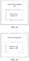
- a signal driving apparatus 200 includes: a signal driving module, configured to: in a first signal driving period, apply non-inverting drive signals to M adjacent detection electrodes and apply inverting drive signals to N adjacent detection electrodes, where the non-inverting drive signals applied to the M adjacent detection electrodes and the inverting drive signals applied to the N adjacent detection electrodes cancel each other out, M+N ⁇ P and
- the detection electrodes are horizontal detection electrodes or longitudinal detection electrodes
- P denotes a number of the horizontal detection electrodes or a number of the longitudinal detection electrodes.
- a number of detection electrodes to which the non-inverting drive signals are applied in the two signal driving periods is greater than or equal to 1.
- the coding module is further configured to: in the first signal driving period, not apply the drive signals to I detection electrodes; in the second signal driving period, not apply the drive signals to O detection electrodes; where the I detection electrodes are located between the M adjacent detection electrodes and the N adjacent detection electrodes, and the O detection electrodes are located between the K adjacent detection electrodes and the L adjacent detection electrodes.
- M-N K-L.
- the detection electrodes are horizontal detection electrodes or longitudinal detection electrodes
- P denotes a number of the horizontal detection electrodes or a number of the longitudinal detection electrodes.
- a number of detection electrodes to which the non-inverting drive signals are applied in two of the three signal driving periods is greater than or equal to 2.
- the signal driving module is further configured to: in the first signal driving period, not apply the drive signals to I detection electrodes, wherein the I detection electrodes are located between the M adjacent detection electrodes and the N adjacent detection electrodes; in the second signal driving period, not apply the drive signals to O detection electrodes, wherein the O detection electrodes are located between the K adjacent detection electrodes and the L adjacent detection electrodes; and in the third signal driving period, not apply the drive signals to P detection electrodes, wherein the P detection electrodes are located between the G adjacent detection electrodes and the H adjacent detection electrodes; wherein I ⁇ B, O ⁇ J and P ⁇ F.
- the detection electrodes are horizontal detection electrodes or longitudinal detection electrodes
- P denotes a number of the horizontal detection electrodes or a number of the longitudinal detection electrodes.
- a number of detection electrodes to which the non-inverting drive signals are applied in two of the four signal driving periods is greater than or equal to 3.
- the signal driving module is further configured to: in the first signal driving period, not apply the drive signals to I detection electrodes, wherein the I detection electrodes are located between the M adjacent detection electrodes and the N adjacent detection electrodes; in the second signal driving period, not apply the drive signals to O detection electrodes, wherein the O detection electrodes are located between the K adjacent detection electrodes and the L adjacent detection electrodes; in the third signal driving period, not apply the drive signals to P detection electrodes, wherein the P detection electrodes are located between the G adjacent detection electrodes and the H adjacent detection electrodes; and in the fourth signal driving period, not apply the drive signals to W detection electrodes, wherein the W detection electrodes are located between the T adjacent detection electrodes and the Y adjacent detection electrodes; wherein I ⁇ B, O ⁇ J, P ⁇ F and W ⁇ U.
- a touch control chip 203 may include the signal driving apparatus 200 shown in FIG. 19 .
Landscapes
- Engineering & Computer Science (AREA)
- General Engineering & Computer Science (AREA)
- Theoretical Computer Science (AREA)
- Human Computer Interaction (AREA)
- Physics & Mathematics (AREA)
- General Physics & Mathematics (AREA)
- Position Input By Displaying (AREA)
- Electronic Switches (AREA)
Applications Claiming Priority (1)
| Application Number | Priority Date | Filing Date | Title |
|---|---|---|---|
| PCT/CN2020/096117 WO2021253164A1 (zh) | 2020-06-15 | 2020-06-15 | 打码方法、打码装置和触控芯片 |
Publications (3)
| Publication Number | Publication Date |
|---|---|
| EP4020143A4 EP4020143A4 (de) | 2022-06-29 |
| EP4020143A1 true EP4020143A1 (de) | 2022-06-29 |
| EP4020143B1 EP4020143B1 (de) | 2023-05-03 |
Family
ID=79268976
Family Applications (1)
| Application Number | Title | Priority Date | Filing Date |
|---|---|---|---|
| EP20926361.5A Active EP4020143B1 (de) | 2020-06-15 | 2020-06-15 | Verfahren zur signalsteuerung, vorrichtung zur signalsteuerung und berührungssteuerungschip |
Country Status (4)
| Country | Link |
|---|---|
| US (2) | US11620018B2 (de) |
| EP (1) | EP4020143B1 (de) |
| CN (1) | CN115427922B (de) |
| WO (1) | WO2021253164A1 (de) |
Families Citing this family (7)
| Publication number | Priority date | Publication date | Assignee | Title |
|---|---|---|---|---|
| CN115427922B (zh) * | 2020-06-15 | 2023-08-25 | 深圳市汇顶科技股份有限公司 | 打码方法、打码装置和触控芯片 |
| KR102876961B1 (ko) * | 2020-08-14 | 2025-10-29 | 삼성디스플레이 주식회사 | 전자 장치 |
| CN115686250A (zh) * | 2021-07-31 | 2023-02-03 | 荣耀终端有限公司 | 刷新率的切换方法、电子设备和系统 |
| KR20230053011A (ko) * | 2021-10-13 | 2023-04-21 | 삼성디스플레이 주식회사 | 전자 장치 |
| KR20250011271A (ko) * | 2023-07-14 | 2025-01-21 | 엘지디스플레이 주식회사 | 터치표시장치, 터치표시장치의 구동방법 |
| US12596450B2 (en) * | 2024-01-02 | 2026-04-07 | Novatek Microelectronics Corp. | Method of controlling touch sensor and related touch sensing circuit |
| KR20260004115A (ko) * | 2024-07-01 | 2026-01-08 | 주식회사 하이딥 | 전자 디바이스 |
Family Cites Families (32)
| Publication number | Priority date | Publication date | Assignee | Title |
|---|---|---|---|---|
| JP4862466B2 (ja) | 2006-04-14 | 2012-01-25 | 富士ゼロックス株式会社 | 下敷き、入力装置及び筆跡情報取得方法 |
| US8279180B2 (en) | 2006-05-02 | 2012-10-02 | Apple Inc. | Multipoint touch surface controller |
| TWI521400B (zh) | 2009-01-06 | 2016-02-11 | Elan Microelectronics Corp | The touch input device and the control method of the touch panel module applied to the touch input device |
| CN102566800B (zh) | 2011-12-29 | 2015-08-12 | 敦泰科技有限公司 | 一种触摸笔、触摸检测方法和触摸检测系统 |
| US9921626B2 (en) | 2012-09-28 | 2018-03-20 | Atmel Corporation | Stylus communication with near-field coupling |
| US10126850B2 (en) | 2013-08-16 | 2018-11-13 | Apple Inc. | Active integrated touch/display |
| WO2015125176A1 (ja) * | 2014-02-21 | 2015-08-27 | パナソニック液晶ディスプレイ株式会社 | タッチ検出機能が一体化された表示装置 |
| US10379694B2 (en) | 2014-08-27 | 2019-08-13 | Samsung Electronics Co., Ltd. | Touch panel and coordinate measuring system having the same |
| US9830000B2 (en) * | 2014-12-12 | 2017-11-28 | Microsoft Technology Licensing, Llc | Active stylus synchronization |
| KR101659036B1 (ko) | 2015-02-04 | 2016-09-23 | 엘지전자 주식회사 | 스타일러스 펜 및 터치 패널을 포함하는 이동 단말기 및 그 제어방법 |
| KR101732957B1 (ko) | 2015-09-22 | 2017-05-08 | 주식회사 에이에프오 | 광학식 터치스크린의 펜 종류 및 방향 인식 장치 |
| US9933891B2 (en) | 2015-11-03 | 2018-04-03 | Microsoft Technology Licensing, Llc | User input comprising an event and detected motion |
| CN105807990B (zh) * | 2016-03-01 | 2018-11-27 | 京东方科技集团股份有限公司 | 显示屏、触控笔以及显示模组 |
| CN107969152A (zh) | 2016-08-26 | 2018-04-27 | 深圳市汇顶科技股份有限公司 | 信号发射方法、信号解析方法、主动笔及触控屏 |
| TWI653568B (zh) | 2016-11-03 | 2019-03-11 | 禾瑞亞科技股份有限公司 | 觸控處理裝置、方法與電子系統 |
| TWI652605B (zh) * | 2017-05-08 | 2019-03-01 | 義隆電子股份有限公司 | 內嵌式觸控顯示裝置及其與主動筆的溝通方法 |
| US10216333B2 (en) * | 2017-06-30 | 2019-02-26 | Microsoft Technology Licensing, Llc | Phase error compensation in single correlator systems |
| US10990221B2 (en) * | 2017-09-29 | 2021-04-27 | Apple Inc. | Multi-power domain touch sensing |
| JP6921978B2 (ja) * | 2017-11-01 | 2021-08-18 | 株式会社ワコム | 位置検出システム及び表示装置の制御回路 |
| WO2019095377A1 (zh) | 2017-11-20 | 2019-05-23 | 深圳市汇顶科技股份有限公司 | 差分电路、电容检测电路、触摸检测装置和终端设备 |
| CN108124499B (zh) * | 2017-12-13 | 2020-08-28 | 深圳市汇顶科技股份有限公司 | 主动笔的信号发生电路、主动笔和打码方法 |
| WO2019113837A1 (zh) | 2017-12-13 | 2019-06-20 | 深圳市汇顶科技股份有限公司 | 确定抵消支路的控制参数的方法及其装置、触控检测装置 |
| US10877578B2 (en) * | 2018-07-18 | 2020-12-29 | Wacom Co., Ltd. | Sensor controller and active pen |
| KR102610819B1 (ko) * | 2018-08-10 | 2023-12-07 | 주식회사 엘엑스세미콘 | 터치구동장치 및 디스플레이장치 |
| KR102496108B1 (ko) * | 2018-08-31 | 2023-02-06 | 주식회사 엘엑스세미콘 | 터치구동장치, 디스플레이시스템 및 액티브펜 |
| US11054935B2 (en) | 2018-11-19 | 2021-07-06 | Beechrock Limited | Stylus with contact sensor |
| JP6952753B2 (ja) | 2019-01-25 | 2021-10-20 | 株式会社ワコム | アクティブペンの位置検出方法及びセンサコントローラ |
| CN110175261A (zh) | 2019-05-29 | 2019-08-27 | 深圳市九州传媒科技有限公司 | 一种防止点读码冲突的系统及方法 |
| CN110321017B (zh) * | 2019-07-29 | 2024-02-02 | 深圳市千分一智能技术有限公司 | 一种主动电容笔的打码电路及打码方法 |
| EP3822747B1 (de) * | 2019-09-30 | 2022-05-11 | Shenzhen Goodix Technology Co., Ltd. | Verfahren zum senden und empfangen von signalen, prozessorchip, aktiver stift und berührungsbildschirm |
| EP3851935B1 (de) | 2019-11-22 | 2022-08-24 | Shenzhen Goodix Technology Co., Ltd. | Druckerkennungsverfahren, gerät und berührungsempfindlicher steuerungschip |
| CN115427922B (zh) * | 2020-06-15 | 2023-08-25 | 深圳市汇顶科技股份有限公司 | 打码方法、打码装置和触控芯片 |
-
2020
- 2020-06-15 CN CN202080100001.7A patent/CN115427922B/zh active Active
- 2020-06-15 WO PCT/CN2020/096117 patent/WO2021253164A1/zh not_active Ceased
- 2020-06-15 EP EP20926361.5A patent/EP4020143B1/de active Active
-
2021
- 2021-10-02 US US17/492,602 patent/US11620018B2/en active Active
-
2023
- 2023-02-15 US US18/169,858 patent/US12197678B2/en active Active
Also Published As
| Publication number | Publication date |
|---|---|
| WO2021253164A1 (zh) | 2021-12-23 |
| US20220027010A1 (en) | 2022-01-27 |
| EP4020143A4 (de) | 2022-06-29 |
| US11620018B2 (en) | 2023-04-04 |
| US12197678B2 (en) | 2025-01-14 |
| US20230195260A1 (en) | 2023-06-22 |
| CN115427922A (zh) | 2022-12-02 |
| CN115427922B (zh) | 2023-08-25 |
| EP4020143B1 (de) | 2023-05-03 |
Similar Documents
| Publication | Publication Date | Title |
|---|---|---|
| US11620018B2 (en) | Signal driving method, signal driving apparatus and touch control chip | |
| CN110892368B (zh) | 传感器控制器 | |
| CN102253745B (zh) | 指示体位置检测装置及指示体位置检测方法 | |
| US20140028607A1 (en) | Device for Digital Communication Through Capacitive Coupling | |
| US11221713B2 (en) | Ultrasonic touch device and MEl'hod, display device | |
| US20150138145A1 (en) | Touch screen controller to generate single-ended touch signal, and touch screen system and display apparatus including the same | |
| JP2017536631A (ja) | タッチ基板、端末、及びタッチの精度を向上させる方法 | |
| WO2022165839A1 (zh) | 抗干扰的方法、触控芯片及主动笔芯片 | |
| CN211787016U (zh) | 主动笔 | |
| TW202331476A (zh) | 觸控筆控制電路及觸控筆 | |
| US11842004B2 (en) | Method of signal transmission, touch control chip and electronic device | |
| CN104503620A (zh) | 一种触摸屏驱动电路、触摸屏和电子终端 | |
| CN104834123A (zh) | 触控显示装置及其控制方法、电路 | |
| CN108809558B (zh) | 一种同步信号块的传输方法、网络设备及用户设备 | |
| CN106527821A (zh) | 触控显示面板的触控驱动方法、触控显示面板及显示装置 | |
| CN112363634B (zh) | 打码方法、打码装置和触控芯片 | |
| US11531425B1 (en) | Inter-band harmonics interference mitigation for multi-frequency-region parallel scan | |
| EP1471411A1 (de) | Elektronische weisse tafel mit flexibilitätsmembran-elektromagnetinduktionserzeugungs einrichtung | |
| US12260048B2 (en) | Display driving method with target report rate | |
| CN112486354A (zh) | 电子设备的触控方法、触控组件的信息传输方法及装置 | |
| WO2022087917A1 (zh) | 噪声检测的方法、主动笔和屏幕 | |
| WO2016043035A1 (ja) | タッチパネル装置 | |
| CN105260051B (zh) | 触控驱动电路及触控显示面板 | |
| KR102018753B1 (ko) | 터치 패널의 구동 장치 및 구동 방법 | |
| US11928287B2 (en) | Touch control chip, coding method and electronic device |
Legal Events
| Date | Code | Title | Description |
|---|---|---|---|
| STAA | Information on the status of an ep patent application or granted ep patent |
Free format text: STATUS: UNKNOWN |
|
| STAA | Information on the status of an ep patent application or granted ep patent |
Free format text: STATUS: THE INTERNATIONAL PUBLICATION HAS BEEN MADE |
|
| PUAI | Public reference made under article 153(3) epc to a published international application that has entered the european phase |
Free format text: ORIGINAL CODE: 0009012 |
|
| STAA | Information on the status of an ep patent application or granted ep patent |
Free format text: STATUS: REQUEST FOR EXAMINATION WAS MADE |
|
| 17P | Request for examination filed |
Effective date: 20210929 |
|
| A4 | Supplementary search report drawn up and despatched |
Effective date: 20220419 |
|
| AK | Designated contracting states |
Kind code of ref document: A1 Designated state(s): AL AT BE BG CH CY CZ DE DK EE ES FI FR GB GR HR HU IE IS IT LI LT LU LV MC MK MT NL NO PL PT RO RS SE SI SK SM TR |
|
| GRAP | Despatch of communication of intention to grant a patent |
Free format text: ORIGINAL CODE: EPIDOSNIGR1 |
|
| STAA | Information on the status of an ep patent application or granted ep patent |
Free format text: STATUS: GRANT OF PATENT IS INTENDED |
|
| DAV | Request for validation of the european patent (deleted) | ||
| DAX | Request for extension of the european patent (deleted) | ||
| INTG | Intention to grant announced |
Effective date: 20230215 |
|
| GRAS | Grant fee paid |
Free format text: ORIGINAL CODE: EPIDOSNIGR3 |
|
| GRAA | (expected) grant |
Free format text: ORIGINAL CODE: 0009210 |
|
| STAA | Information on the status of an ep patent application or granted ep patent |
Free format text: STATUS: THE PATENT HAS BEEN GRANTED |
|
| AK | Designated contracting states |
Kind code of ref document: B1 Designated state(s): AL AT BE BG CH CY CZ DE DK EE ES FI FR GB GR HR HU IE IS IT LI LT LU LV MC MK MT NL NO PL PT RO RS SE SI SK SM TR |
|
| REG | Reference to a national code |
Ref country code: GB Ref legal event code: FG4D |
|
| REG | Reference to a national code |
Ref country code: AT Ref legal event code: REF Ref document number: 1565208 Country of ref document: AT Kind code of ref document: T Effective date: 20230515 Ref country code: CH Ref legal event code: EP |
|
| REG | Reference to a national code |
Ref country code: DE Ref legal event code: R096 Ref document number: 602020010538 Country of ref document: DE |
|
| REG | Reference to a national code |
Ref country code: IE Ref legal event code: FG4D |
|
| P01 | Opt-out of the competence of the unified patent court (upc) registered |
Effective date: 20230507 |
|
| REG | Reference to a national code |
Ref country code: LT Ref legal event code: MG9D |
|
| REG | Reference to a national code |
Ref country code: NL Ref legal event code: MP Effective date: 20230503 |
|
| REG | Reference to a national code |
Ref country code: AT Ref legal event code: MK05 Ref document number: 1565208 Country of ref document: AT Kind code of ref document: T Effective date: 20230503 |
|
| PG25 | Lapsed in a contracting state [announced via postgrant information from national office to epo] |
Ref country code: SE Free format text: LAPSE BECAUSE OF FAILURE TO SUBMIT A TRANSLATION OF THE DESCRIPTION OR TO PAY THE FEE WITHIN THE PRESCRIBED TIME-LIMIT Effective date: 20230503 Ref country code: PT Free format text: LAPSE BECAUSE OF FAILURE TO SUBMIT A TRANSLATION OF THE DESCRIPTION OR TO PAY THE FEE WITHIN THE PRESCRIBED TIME-LIMIT Effective date: 20230904 Ref country code: NO Free format text: LAPSE BECAUSE OF FAILURE TO SUBMIT A TRANSLATION OF THE DESCRIPTION OR TO PAY THE FEE WITHIN THE PRESCRIBED TIME-LIMIT Effective date: 20230803 Ref country code: NL Free format text: LAPSE BECAUSE OF FAILURE TO SUBMIT A TRANSLATION OF THE DESCRIPTION OR TO PAY THE FEE WITHIN THE PRESCRIBED TIME-LIMIT Effective date: 20230503 Ref country code: ES Free format text: LAPSE BECAUSE OF FAILURE TO SUBMIT A TRANSLATION OF THE DESCRIPTION OR TO PAY THE FEE WITHIN THE PRESCRIBED TIME-LIMIT Effective date: 20230503 Ref country code: AT Free format text: LAPSE BECAUSE OF FAILURE TO SUBMIT A TRANSLATION OF THE DESCRIPTION OR TO PAY THE FEE WITHIN THE PRESCRIBED TIME-LIMIT Effective date: 20230503 |
|
| PG25 | Lapsed in a contracting state [announced via postgrant information from national office to epo] |
Ref country code: RS Free format text: LAPSE BECAUSE OF FAILURE TO SUBMIT A TRANSLATION OF THE DESCRIPTION OR TO PAY THE FEE WITHIN THE PRESCRIBED TIME-LIMIT Effective date: 20230503 Ref country code: PL Free format text: LAPSE BECAUSE OF FAILURE TO SUBMIT A TRANSLATION OF THE DESCRIPTION OR TO PAY THE FEE WITHIN THE PRESCRIBED TIME-LIMIT Effective date: 20230503 Ref country code: LV Free format text: LAPSE BECAUSE OF FAILURE TO SUBMIT A TRANSLATION OF THE DESCRIPTION OR TO PAY THE FEE WITHIN THE PRESCRIBED TIME-LIMIT Effective date: 20230503 Ref country code: LT Free format text: LAPSE BECAUSE OF FAILURE TO SUBMIT A TRANSLATION OF THE DESCRIPTION OR TO PAY THE FEE WITHIN THE PRESCRIBED TIME-LIMIT Effective date: 20230503 Ref country code: IS Free format text: LAPSE BECAUSE OF FAILURE TO SUBMIT A TRANSLATION OF THE DESCRIPTION OR TO PAY THE FEE WITHIN THE PRESCRIBED TIME-LIMIT Effective date: 20230903 Ref country code: HR Free format text: LAPSE BECAUSE OF FAILURE TO SUBMIT A TRANSLATION OF THE DESCRIPTION OR TO PAY THE FEE WITHIN THE PRESCRIBED TIME-LIMIT Effective date: 20230503 Ref country code: GR Free format text: LAPSE BECAUSE OF FAILURE TO SUBMIT A TRANSLATION OF THE DESCRIPTION OR TO PAY THE FEE WITHIN THE PRESCRIBED TIME-LIMIT Effective date: 20230804 |
|
| PG25 | Lapsed in a contracting state [announced via postgrant information from national office to epo] |
Ref country code: FI Free format text: LAPSE BECAUSE OF FAILURE TO SUBMIT A TRANSLATION OF THE DESCRIPTION OR TO PAY THE FEE WITHIN THE PRESCRIBED TIME-LIMIT Effective date: 20230503 |
|
| PG25 | Lapsed in a contracting state [announced via postgrant information from national office to epo] |
Ref country code: SK Free format text: LAPSE BECAUSE OF FAILURE TO SUBMIT A TRANSLATION OF THE DESCRIPTION OR TO PAY THE FEE WITHIN THE PRESCRIBED TIME-LIMIT Effective date: 20230503 |
|
| PG25 | Lapsed in a contracting state [announced via postgrant information from national office to epo] |
Ref country code: SM Free format text: LAPSE BECAUSE OF FAILURE TO SUBMIT A TRANSLATION OF THE DESCRIPTION OR TO PAY THE FEE WITHIN THE PRESCRIBED TIME-LIMIT Effective date: 20230503 Ref country code: SK Free format text: LAPSE BECAUSE OF FAILURE TO SUBMIT A TRANSLATION OF THE DESCRIPTION OR TO PAY THE FEE WITHIN THE PRESCRIBED TIME-LIMIT Effective date: 20230503 Ref country code: RO Free format text: LAPSE BECAUSE OF FAILURE TO SUBMIT A TRANSLATION OF THE DESCRIPTION OR TO PAY THE FEE WITHIN THE PRESCRIBED TIME-LIMIT Effective date: 20230503 Ref country code: EE Free format text: LAPSE BECAUSE OF FAILURE TO SUBMIT A TRANSLATION OF THE DESCRIPTION OR TO PAY THE FEE WITHIN THE PRESCRIBED TIME-LIMIT Effective date: 20230503 Ref country code: DK Free format text: LAPSE BECAUSE OF FAILURE TO SUBMIT A TRANSLATION OF THE DESCRIPTION OR TO PAY THE FEE WITHIN THE PRESCRIBED TIME-LIMIT Effective date: 20230503 Ref country code: CZ Free format text: LAPSE BECAUSE OF FAILURE TO SUBMIT A TRANSLATION OF THE DESCRIPTION OR TO PAY THE FEE WITHIN THE PRESCRIBED TIME-LIMIT Effective date: 20230503 |
|
| REG | Reference to a national code |
Ref country code: CH Ref legal event code: PL |
|
| REG | Reference to a national code |
Ref country code: DE Ref legal event code: R097 Ref document number: 602020010538 Country of ref document: DE |
|
| REG | Reference to a national code |
Ref country code: BE Ref legal event code: MM Effective date: 20230630 |
|
| PG25 | Lapsed in a contracting state [announced via postgrant information from national office to epo] |
Ref country code: MC Free format text: LAPSE BECAUSE OF FAILURE TO SUBMIT A TRANSLATION OF THE DESCRIPTION OR TO PAY THE FEE WITHIN THE PRESCRIBED TIME-LIMIT Effective date: 20230503 |
|
| PG25 | Lapsed in a contracting state [announced via postgrant information from national office to epo] |
Ref country code: MC Free format text: LAPSE BECAUSE OF FAILURE TO SUBMIT A TRANSLATION OF THE DESCRIPTION OR TO PAY THE FEE WITHIN THE PRESCRIBED TIME-LIMIT Effective date: 20230503 |
|
| PG25 | Lapsed in a contracting state [announced via postgrant information from national office to epo] |
Ref country code: LU Free format text: LAPSE BECAUSE OF NON-PAYMENT OF DUE FEES Effective date: 20230615 |
|
| PLBE | No opposition filed within time limit |
Free format text: ORIGINAL CODE: 0009261 |
|
| STAA | Information on the status of an ep patent application or granted ep patent |
Free format text: STATUS: NO OPPOSITION FILED WITHIN TIME LIMIT |
|
| REG | Reference to a national code |
Ref country code: IE Ref legal event code: MM4A |
|
| PG25 | Lapsed in a contracting state [announced via postgrant information from national office to epo] |
Ref country code: LU Free format text: LAPSE BECAUSE OF NON-PAYMENT OF DUE FEES Effective date: 20230615 |
|
| 26N | No opposition filed |
Effective date: 20240206 |
|
| PG25 | Lapsed in a contracting state [announced via postgrant information from national office to epo] |
Ref country code: IE Free format text: LAPSE BECAUSE OF NON-PAYMENT OF DUE FEES Effective date: 20230615 |
|
| PG25 | Lapsed in a contracting state [announced via postgrant information from national office to epo] |
Ref country code: IE Free format text: LAPSE BECAUSE OF NON-PAYMENT OF DUE FEES Effective date: 20230615 Ref country code: CH Free format text: LAPSE BECAUSE OF NON-PAYMENT OF DUE FEES Effective date: 20230630 |
|
| PG25 | Lapsed in a contracting state [announced via postgrant information from national office to epo] |
Ref country code: SI Free format text: LAPSE BECAUSE OF FAILURE TO SUBMIT A TRANSLATION OF THE DESCRIPTION OR TO PAY THE FEE WITHIN THE PRESCRIBED TIME-LIMIT Effective date: 20230503 |
|
| PG25 | Lapsed in a contracting state [announced via postgrant information from national office to epo] |
Ref country code: SI Free format text: LAPSE BECAUSE OF FAILURE TO SUBMIT A TRANSLATION OF THE DESCRIPTION OR TO PAY THE FEE WITHIN THE PRESCRIBED TIME-LIMIT Effective date: 20230503 Ref country code: IT Free format text: LAPSE BECAUSE OF FAILURE TO SUBMIT A TRANSLATION OF THE DESCRIPTION OR TO PAY THE FEE WITHIN THE PRESCRIBED TIME-LIMIT Effective date: 20230503 Ref country code: FR Free format text: LAPSE BECAUSE OF NON-PAYMENT OF DUE FEES Effective date: 20230703 Ref country code: BE Free format text: LAPSE BECAUSE OF NON-PAYMENT OF DUE FEES Effective date: 20230630 |
|
| PG25 | Lapsed in a contracting state [announced via postgrant information from national office to epo] |
Ref country code: BG Free format text: LAPSE BECAUSE OF FAILURE TO SUBMIT A TRANSLATION OF THE DESCRIPTION OR TO PAY THE FEE WITHIN THE PRESCRIBED TIME-LIMIT Effective date: 20230503 |
|
| PG25 | Lapsed in a contracting state [announced via postgrant information from national office to epo] |
Ref country code: BG Free format text: LAPSE BECAUSE OF FAILURE TO SUBMIT A TRANSLATION OF THE DESCRIPTION OR TO PAY THE FEE WITHIN THE PRESCRIBED TIME-LIMIT Effective date: 20230503 |
|
| PGFP | Annual fee paid to national office [announced via postgrant information from national office to epo] |
Ref country code: DE Payment date: 20250624 Year of fee payment: 6 |
|
| PGFP | Annual fee paid to national office [announced via postgrant information from national office to epo] |
Ref country code: GB Payment date: 20250626 Year of fee payment: 6 |
|
| PG25 | Lapsed in a contracting state [announced via postgrant information from national office to epo] |
Ref country code: CY Free format text: LAPSE BECAUSE OF FAILURE TO SUBMIT A TRANSLATION OF THE DESCRIPTION OR TO PAY THE FEE WITHIN THE PRESCRIBED TIME-LIMIT; INVALID AB INITIO Effective date: 20200615 |
|
| PG25 | Lapsed in a contracting state [announced via postgrant information from national office to epo] |
Ref country code: HU Free format text: LAPSE BECAUSE OF FAILURE TO SUBMIT A TRANSLATION OF THE DESCRIPTION OR TO PAY THE FEE WITHIN THE PRESCRIBED TIME-LIMIT; INVALID AB INITIO Effective date: 20200615 |
|
| PG25 | Lapsed in a contracting state [announced via postgrant information from national office to epo] |
Ref country code: TR Free format text: LAPSE BECAUSE OF FAILURE TO SUBMIT A TRANSLATION OF THE DESCRIPTION OR TO PAY THE FEE WITHIN THE PRESCRIBED TIME-LIMIT Effective date: 20230503 |