EP4018331B1 - Method and system for auto-addressing nodes on a communication bus - Google Patents
Method and system for auto-addressing nodes on a communication bus Download PDFInfo
- Publication number
- EP4018331B1 EP4018331B1 EP20858582.8A EP20858582A EP4018331B1 EP 4018331 B1 EP4018331 B1 EP 4018331B1 EP 20858582 A EP20858582 A EP 20858582A EP 4018331 B1 EP4018331 B1 EP 4018331B1
- Authority
- EP
- European Patent Office
- Prior art keywords
- satellite
- module
- communication bus
- address
- mcu
- Prior art date
- Legal status (The legal status is an assumption and is not a legal conclusion. Google has not performed a legal analysis and makes no representation as to the accuracy of the status listed.)
- Active
Links
Images


Classifications
-
- G—PHYSICS
- G06—COMPUTING OR CALCULATING; COUNTING
- G06F—ELECTRIC DIGITAL DATA PROCESSING
- G06F13/00—Interconnection of, or transfer of information or other signals between, memories, input/output devices or central processing units
- G06F13/38—Information transfer, e.g. on bus
- G06F13/40—Bus structure
- G06F13/4004—Coupling between buses
- G06F13/4027—Coupling between buses using bus bridges
- G06F13/404—Coupling between buses using bus bridges with address mapping
-
- G—PHYSICS
- G06—COMPUTING OR CALCULATING; COUNTING
- G06F—ELECTRIC DIGITAL DATA PROCESSING
- G06F13/00—Interconnection of, or transfer of information or other signals between, memories, input/output devices or central processing units
- G06F13/38—Information transfer, e.g. on bus
- G06F13/42—Bus transfer protocol, e.g. handshake; Synchronisation
- G06F13/4247—Bus transfer protocol, e.g. handshake; Synchronisation on a daisy chain bus
-
- H—ELECTRICITY
- H03—ELECTRONIC CIRCUITRY
- H03K—PULSE TECHNIQUE
- H03K17/00—Electronic switching or gating, i.e. not by contact-making and –breaking
- H03K17/51—Electronic switching or gating, i.e. not by contact-making and –breaking characterised by the components used
- H03K17/56—Electronic switching or gating, i.e. not by contact-making and –breaking characterised by the components used by the use, as active elements, of semiconductor devices
- H03K17/687—Electronic switching or gating, i.e. not by contact-making and –breaking characterised by the components used by the use, as active elements, of semiconductor devices the devices being field-effect transistors
-
- H—ELECTRICITY
- H04—ELECTRIC COMMUNICATION TECHNIQUE
- H04L—TRANSMISSION OF DIGITAL INFORMATION, e.g. TELEGRAPHIC COMMUNICATION
- H04L12/00—Data switching networks
- H04L12/02—Details
- H04L12/12—Arrangements for remote connection or disconnection of substations or of equipment thereof
-
- H—ELECTRICITY
- H04—ELECTRIC COMMUNICATION TECHNIQUE
- H04L—TRANSMISSION OF DIGITAL INFORMATION, e.g. TELEGRAPHIC COMMUNICATION
- H04L12/00—Data switching networks
- H04L12/28—Data switching networks characterised by path configuration, e.g. LAN [Local Area Networks] or WAN [Wide Area Networks]
- H04L12/40—Bus networks
- H04L12/40006—Architecture of a communication node
- H04L12/40013—Details regarding a bus controller
-
- H—ELECTRICITY
- H04—ELECTRIC COMMUNICATION TECHNIQUE
- H04L—TRANSMISSION OF DIGITAL INFORMATION, e.g. TELEGRAPHIC COMMUNICATION
- H04L12/00—Data switching networks
- H04L12/28—Data switching networks characterised by path configuration, e.g. LAN [Local Area Networks] or WAN [Wide Area Networks]
- H04L12/40—Bus networks
- H04L12/40006—Architecture of a communication node
- H04L12/40019—Details regarding a bus master
-
- H—ELECTRICITY
- H04—ELECTRIC COMMUNICATION TECHNIQUE
- H04L—TRANSMISSION OF DIGITAL INFORMATION, e.g. TELEGRAPHIC COMMUNICATION
- H04L12/00—Data switching networks
- H04L12/64—Hybrid switching systems
- H04L12/6418—Hybrid transport
-
- H—ELECTRICITY
- H03—ELECTRONIC CIRCUITRY
- H03K—PULSE TECHNIQUE
- H03K19/00—Logic circuits, i.e. having at least two inputs acting on one output; Inverting circuits
- H03K19/0175—Coupling arrangements; Interface arrangements
- H03K19/0185—Coupling arrangements; Interface arrangements using field effect transistors only
- H03K19/018507—Interface arrangements
-
- H—ELECTRICITY
- H03—ELECTRONIC CIRCUITRY
- H03K—PULSE TECHNIQUE
- H03K2217/00—Indexing scheme related to electronic switching or gating, i.e. not by contact-making or -breaking covered by H03K17/00
- H03K2217/0072—Low side switches, i.e. the lower potential [DC] or neutral wire [AC] being directly connected to the switch and not via the load
-
- H—ELECTRICITY
- H04—ELECTRIC COMMUNICATION TECHNIQUE
- H04L—TRANSMISSION OF DIGITAL INFORMATION, e.g. TELEGRAPHIC COMMUNICATION
- H04L12/00—Data switching networks
- H04L12/28—Data switching networks characterised by path configuration, e.g. LAN [Local Area Networks] or WAN [Wide Area Networks]
- H04L12/40—Bus networks
- H04L2012/40208—Bus networks characterized by the use of a particular bus standard
- H04L2012/40215—Controller Area Network CAN
-
- H—ELECTRICITY
- H04—ELECTRIC COMMUNICATION TECHNIQUE
- H04L—TRANSMISSION OF DIGITAL INFORMATION, e.g. TELEGRAPHIC COMMUNICATION
- H04L12/00—Data switching networks
- H04L12/64—Hybrid switching systems
- H04L12/6418—Hybrid transport
- H04L2012/6421—Medium of transmission, e.g. fibre, cable, radio, satellite
-
- H—ELECTRICITY
- H04—ELECTRIC COMMUNICATION TECHNIQUE
- H04W—WIRELESS COMMUNICATION NETWORKS
- H04W4/00—Services specially adapted for wireless communication networks; Facilities therefor
- H04W4/80—Services using short range communication, e.g. near-field communication [NFC], radio-frequency identification [RFID] or low energy communication
-
- Y—GENERAL TAGGING OF NEW TECHNOLOGICAL DEVELOPMENTS; GENERAL TAGGING OF CROSS-SECTIONAL TECHNOLOGIES SPANNING OVER SEVERAL SECTIONS OF THE IPC; TECHNICAL SUBJECTS COVERED BY FORMER USPC CROSS-REFERENCE ART COLLECTIONS [XRACs] AND DIGESTS
- Y02—TECHNOLOGIES OR APPLICATIONS FOR MITIGATION OR ADAPTATION AGAINST CLIMATE CHANGE
- Y02D—CLIMATE CHANGE MITIGATION TECHNOLOGIES IN INFORMATION AND COMMUNICATION TECHNOLOGIES [ICT], I.E. INFORMATION AND COMMUNICATION TECHNOLOGIES AIMING AT THE REDUCTION OF THEIR OWN ENERGY USE
- Y02D30/00—Reducing energy consumption in communication networks
- Y02D30/50—Reducing energy consumption in communication networks in wire-line communication networks, e.g. low power modes or reduced link rate
Definitions
- the smart key module system includes a central module and several satellite modules distributed throughout the body of the car, each with a receiver capable of receiving a signal from a key fob or smart phone.
- a typical system will have multiple satellite modules, between eight and twelve in some cases, in addition to a central module. It is desired that the PEPS system be able to determine when the driver is within the unlocking zone of the vehicle (1-2M away), and the approximate location of the key holder. This is done by triangulating the signals received by the various satellite (or slave) modules that are distributed throughout the car in numerous known locations such as the passenger side door, behind seat cushions, rocker panel, trunk, or rear bumper.
- a master or central module communicates with the satellite or slave modules using a communication interface on the automobile's Controller Area Network (CAN) bus.
- the central module addresses each satellite module for data related to gaining entry access to the car so that the central module can determine whether to grant entry access to the car or allow the driver to start driving the car after gaining access.
- the central module In order to triangulate the signals received from the satellite modules and determine the location of the key fob, the central module must know the location of each satellite module sending data to it.
- the central module is able to determine which satellite module it is receiving data from based on the bus address of the satellite module sending the data because the central module knows the sequence order of satellite bus address assignment. In this way, the central module correlates the communication bus address to the location of the satellite in the automobile.
- LIN Local Interconnect Network
- the central module sends an address to the first satellite over the LIN bus, and then the first satellite will send an address received from the central module to the second satellite using the LIN bus. This process continues until all the satellite modules have been addressed.
- This scheme requires two LIN physical layers (PHYs) per satellite module as well as one for the master or central module. On the satellite modules, one LIN PHY is for receiving data and one for transmitting data.
- the LIN PHYs are only used for the auto-addressing operation, not for standard data communications which is done on the CAN bus or a different network bus.
- a typical automobile might have 12 satellite modules.
- US2010185784A1 discloses an automatic address assignment for communication bus.
- US2018013578A1 discloses identifying and configuring multiple smart devices on a can bus.
- Disclosed embodiments describe a scheme for auto addressing satellite modules on a communication bus, such as CAN, without the need for a separate bus, such as LIN, with transceivers in each module dedicated to the auto addressing function.
- a nominal 12 volt battery level signal is daisy-chained to the satellite modules in order to sequentially wake each of the satellite module alerting it to listen to the CAN bus to receive its address assignment.
- the newly addressed satellite module then sends an acknowledgment signal back on the communication bus to the central module and sends a 12 volt battery voltage level wake signal to the next satellite module in the sequence.
- Disclosed embodiments include using an n-channel MOSFET as a low side switch to deliver the auto address wake signal, which is preferably a pulse-width-modulated signal for improved noise immunity.
- Disclosed embodiments also include a voltage divider circuit to step down the auto address wake signal from battery voltage level to levels acceptable for a microcontroller input. This circuit also includes current limiting resistors for short circuit and battery load dump surge protection.
- disclosed embodiments include a mechanism for detecting shorts and open circuits in the satellite modules or associated wiring by alerting when a satellite module fails to report it has received its auto address wake signal.
- the central module will know the location of the satellite module indicating a fault because the address the central module is assigning will always be assigned to the satellite module at a given known location.
- CAN is a specialized internal communications network that interconnects components inside a vehicle serial bus standard designed to allow microcontrollers and devices to communicate with each other in applications without a host computer.
- Two or more nodes are required on the CAN network to communicate. The nodes are connected to each other through a two-wire serial bus. Each node requires a central processing unit to interpret the messages it receives and what messages it wants to transmit, a CAN controller which is often integrated into the processing unit, and a CAN transceiver. Each node is able to send and receive messages, but not simultaneously.
- a message or frame consists primarily of the identifier (address) and up to eight data bytes.
- a cyclic redundancy check (CRC), acknowledge slot (ACK) and other overhead are also part of the message.
- the CAN bus was originally designed for automobiles, but is used in numerous other contexts as well, such as aviation and navigation, elevators and escalators, industrial and building automation and medical equipment.
- the present invention is applicable to all CAN bus applications involving multiple slave or satellite nodes. Additionally, this invention also may be used with any serial communication bus system having a central or master unit and one or more slave or satellite units, such as LIN bus.
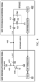
- Figure 1 illustrates a system diagram of a communication bus auto-addressing scheme.
- the system includes a central module 110 that serves as the master on the CAN bus 120. Satellite modules, which are located at various known positions throughout the automobile, are configured as slaves on the communication bus.
- Figure 1 shows a system with a central module and six satellite modules. However, there could be more or less than six satellite modules depending upon system requirements.
- the satellite modules are daisy-chained together via input and output signals wherein the output signal of one satellite module is the input signal for the next satellite module. They also share a common bus data connection along with the central module, which could be a CAN bus, LIN bus, or another type of serial communication bus. For purposes of illustration, an embodiment with CAN bus will be shown here.
- the first satellite module is shown as 130 in the figure and is connected to the central module 110 along with each of the other satellite modules via the communication bus 120.
- the first satellite module 130 is also connected to the central module 110 and to the second satellite module 140 via input and output lines.
- the second satellite module 140 is connected to the first satellite module 130 and to the third satellite module 150 via input and output lines. Satellite modules 4, 5, and 6 are denoted in the figure as 160, 170, and 180, respectively.
- Data communication on the communication bus 120 is bidirectional meaning that each module can send to and receive from the other modules on the bus.
- Each node is able to send and receive messages, but not simultaneously.
- There is an arbitration method in the CAN bus standard to handle collisions on the bus. To enable communication, each node on the bus must be assigned an address and will ignore bus communication unless it is sent to its address.
- the bus addresses on the communication bus are assigned to each satellite module sequentially and in a known order.
- the central module is programmed to know the location where each module is installed.
- the satellite modules are daisy-chained in a preset known order, so that each time a bus address is assigned to a satellite module, the location of the satellite module is known by where it is in the daisy-chain order. In this way, a particular bus address will always correspond to a known satellite module whose location is known. Therefore, the satellite module bus address can always be used to correlate to the exact location of the satellite module. This is necessary for being able to triangulate the signals from multiple satellite modules to determine the approximate location of a PEPS key holder. This is also useful for determining the location of faulty wiring or a faulty satellite module in the event where a particular satellite module with a known bus address fails to acknowledge to the central module that it has been successfully addressed.
- FIG. 2 shows a state diagram for an example embodiment of an auto addressing scheme 200 for satellite modules according to an aspect of the present disclosure.
- the auto addressing scheme 200 begins with power up 210.
- each of the satellite modules is in the default address state 220 during which its communication bus response 250 to data on the bus is to ignore all messages and data on the communication bus.
- Each satellite module 130-180 ignores all data on the communication bus because it does not yet have an address assigned to it, so the satellite modules cannot determine if the data on the bus is intended for it. Therefore, it ignores the data until it is later awakened by a signal that a valid address for that module is on the bus ready to be received.
- the central module 110 from figure 1 sends a signal 230 using its low side switch to the first satellite module 130 indicating that the central module is ready to assign a communication bus address to it.
- the signal 230 could be in the form of a single pulse, a series of pulses, a pulse-width-modulated signal, or any other series of patterned pulses which a microcontroller in the satellite module being addressed compares to the expected signal and validates. Since this signal 230 is not sent via the communication bus, but is instead a separate signal sent only to the first satellite module 130, the other satellite modules 140-180 do not receive signal 230 from the central module 110.
- the satellite module 130 Upon receiving the signal 230 that the central module is ready to send the first address, the satellite module 130 enters the address assignment state 240 and waits for the central module 110 to send an address.
- the bus response 270 of satellite module 130 is now to ignore all messages on the communication bus except for the address assignment message.
- the remaining satellite modules 140-180 remain in the default address state 220 and their communication bus response 250 remains to ignore all messages and data on the communication bus.
- the central module 110 then sends an address assignment message for satellite module 130 via the communication bus. Since satellite module 130 is the only module on the bus waiting to receive an address assignment, it assigns the received address to itself while the other satellite modules continue to ignore the message on the bus.
- satellite module 130 After assigning itself the received address, satellite module 130 exits the address assignment state 240 and sends an acknowledgment message back to the central module via the communication bus notifying the central module that it has received its address.
- the satellite module 130 is now in the addressed state 260 and its communication bus response 290 to data on the bus is to respond to all communication bus messages where the bus address matches its assigned address.
- a similar process then begins for addressing the second satellite module.
- satellite module 130 uses its low side switch to send a signal 230 to the next satellite module 140 indicating that a communication bus address is ready to be assigned to satellite module 140.
- Satellite module 140 then enters the address assignment state 240 and waits for the central module 110 to send an address.
- the bus response 250 of satellite module 140 is now to ignore all messages on the communication bus except for the address assignment message.
- satellite modules 150-180 remain in the default address state 220 and their communication bus response 250 continues to be ignore all messages and data on the communication bus, and satellite module 130 will only respond to messages that have its assigned address.
- the central module 110 then sends an address assignment message for satellite module 140 via the communication bus.
- Satellite module 130 has been addressed and can see that this message is not being sent to its address, so it ignores the message.
- Satellite modules 150-180 are still in the default address state, so they continue to ignore all data on the communication bus. Since satellite module 140 is the only module on the bus waiting to receive an address assignment, it assigns the address on the communication bus to itself while each of the other satellite modules ignores the data on the bus.
- satellite module 140 After assigning itself the address, satellite module 140 exits the address assignment state 240 and sends an acknowledgment message back to the central module via the communication bus notifying the central module that it has received its address.
- the satellite module 140 is now in the addressed state 260 and its communication bus response 290 to data on the bus is to respond to all communication bus messages where the address matches its assigned address. The same process is repeated until all satellite modules have their address assigned.
- Figure 1 shows a system with six satellite modules, the process of Figure 2 can be used with any number of satellite modules two or greater.
- a satellite module receives an address assignment message and already has a valid address assignment. This can occur in situations where for instance, that particular satellite module has previously been in the system and was already assigned a bus address.
- the bus address may have been stored in static memory, allowing the satellite module to retain its address. If this occurs, that satellite module will send an acknowledgment message back to the central module indicating that it has a valid bus address and will send an address assignment message to the next satellite module in the chain.
- Figure 3 shows an example embodiment of a circuit diagram illustrating the interconnection between the central module and the satellite modules. For the sake of simplicity, only two satellite modules are shown in the figure, but there could also be any greater number of satellite modules in the system.
- a central module 310 is shown coupled to a first satellite module 340 by general purpose input/output (GPIO), and satellite module 340 is also coupled to satellite module 370 by GPIO. Additionally, central unit 310, satellite module 340 and satellite module 370 are interconnected via a common bus, which is shown as a CAN bus, but could also be LIN bus or another type of serial communication bus.
- GPIO general purpose input/output
- central unit 310, satellite module 340 and satellite module 370 are interconnected via a common bus, which is shown as a CAN bus, but could also be LIN bus or another type of serial communication bus.
- the central module 310 includes a battery voltage input 312 coupled to the anode of diode 314 which protects the system against back surges on the battery line and the reversal of battery polarity.
- the cathode of diode 314 is coupled to the input of a power converter 316, a communications physical layer (Comm PHY) 318, and to the drain of an n-channel metal oxide semiconductor field effect transistor (MOSFET) 320, which is the low side switch for the central module 310.
- the coupling between the cathode of diode 314 and the drain of low side switch 320 could be direct or through a resistor.
- a n-channel MOSFET is only one example of a switch that can be used for the low side switch. Other types of switches could be used in other embodiments.
- the Comm PHY 318 is coupled to MCU 322 which has a GPIO 324 that is coupled to the gate of low side switch 320.
- the source of low side switch 320 is coupled to ground.
- the Comm PHY 318 is also coupled to microcontroller unit (MCU) 322 and to the Comm PHY 342 of the first satellite module 340 through the communications bus (Comm Bus) 360 and communicates with each of them bidirectionally.
- the drain of the low side switch 320 of the central module 310 is resistively coupled to the gate of the low side switch 350 of the first satellite module 340.
- the first satellite module 340 includes a battery voltage input 312 coupled to the anode of diode 344 which protects the module against back surges on the battery line and the reversal of battery polarity.
- the cathode of diode 344 is coupled to a communications physical layer (Comm PHY) 342 which is coupled to and provides the input for a power converter 336 which provides power for MCU 338.
- the power converter 336 may receive an input from the cathode of diode 344.
- the Comm PHY 342 is coupled to MCU 338 which has a GPIO 354 that is coupled to the gate of low side switch 350.
- the source of low side switch 350 is coupled to ground and the drain is resistively coupled to the cathode of diode 344.
- the Comm PHY 342 is also coupled to MCU 338 and to the Comm PHY 372 of the second satellite module 370 through the Comm Bus 360 and communicates with each of them bidirectionally.
- the drain of low side switch 350 of the first satellite module 340 is resistively coupled to the gate of low side switch 362 of the second satellite module 370.
- the second satellite module 370 is an identical design to the first satellite module 340 with Comm PHY 372, MCU 368, power converter 366, low side switch 362 and diode 374.
- Comm PHY 372, MCU 368, power converter 366, low side switch 362 and diode 374 For simplicity, only two satellite modules are shown in the figure, but there may be more than two satellite modules in the system which would also be of the identical design and would be daisy-chained in like manner with the drain of each low side switch resistively coupled to the gate of the low side switch of the next satellite module.
- satellite modules 340 and 370 are in the default address state 220 and will ignore all messages and data on the communication bus because they do not yet have an address assigned to them. Since the satellite module cannot determine if the data on the bus is intended for it, it ignores all data.
- the MCU 322 and Comm PHY 318 go through their initiation routines.
- Auto addressing of the satellite modules begins with MCU 322 outputting a pulse or series of pulses through a general purpose output node 324 which is coupled to the gate of low side switch 320.
- the series of pulses is a pulse-width-modulated (PWM) pattern for improved noise immunity.
- PWM pulse-width-modulated
- the drain of the low side switch 320 receives the battery supply voltage input from the cathode of diode 314 and the source is coupled to ground. With no input to the gate of low side switch 320, the voltage at 330 is near the upper rail, and when the voltage at the gate of low side switch 320 is high, the voltage at 330 is near ground.
- a PWM pattern is sent from MCU 322 causing the output 330 of low side switch 320 to send a PWM pattern to satellite 340, where a voltage divider made up of resistors 346 and 348 step the battery voltage down to a level tolerable to MCU 338 which receives the pattern at its GPIO.
- satellite module 340 enters the address assignment state 240 and begins listening to the communication bus through its Comm PHY 342 which is receiving messages sent from the central module 310 through its Comm PHY 318 on the communication bus 360.
- the central module 310 is constantly sending data over the communication bus 360 to a default ID with the new address for the satellite node. Once satellite module 340 has received the address, it enters the addressed state 260 and sends an acknowledge message back to the central module MCU 322 via the communication bus 360 causing the central module to increment to the next address in its predetermined pattern. Satellite module 340 then continues the process by sending a signal to satellite module 370 to begin its auto addressing.
- a PWM pattern is sent from MCU 338 causing the output 380 of low side switch 350 to send a PWM pattern to satellite 370, where a voltage divider made up of resistors 376 and 378 step the battery voltage down to a level tolerable to MCU 368 which receives the pattern.
- satellite module 370 enters the address assignment state 240 and begins listening to the communication bus through its Comm PHY 372 which is receiving messages sent from the central module 310 through its Comm PHY 318 on the communication bus 360.
- the central module 310 is constantly sending data over the communication bus 360 to a default ID with the new address for the satellite module. Once satellite module 370 has received the address, it enters the addressed state 260 and sends an acknowledge message back to the central module MCU 322 via the communication bus 360. If there are more satellite modules to be addressed, then the process will repeat with low side switch 362 sending a PWM pattern to the next satellite module and the central module sending the next address to the default ID via the communication bus. This process will continue until all satellite modules have been addressed.
- This auto addressing scheme allows shorts and ground faults in satellite modules to be detected and be reported by the central module as the auto addressing process occurs. Occurrences of opens and shorts are particularly prevalent in automobiles where an increased rate of wiring harness issues may occur. If there is a short to ground or to battery on the auto-addressing line, the central module will never receive the acknowledge message from the satellite module that is being addressed. The central module will be able to report the approximate area where the fault occurred because it knows which satellite module failed to send a proper acknowledgment signal, and it further knows the location of the faulty satellite module because the address the central module is assigning will always be assigned to the satellite module in a specific known location of the vehicle. This report can be sent, for instance, to external circuitry or to a central processing unit to determine what action to take.
- the auto addressing scheme can be run to address the replaced module.
- the majority of satellite modules will already have a communications bus address. If a satellite module already has an address when the auto address process is run, it will send an acknowledge signal back to the central module and the process continue. In this situation where the satellite module that already has an address receives the auto address signal, 330 or 380 in Figure 3 , the satellite module will just send the acknowledge message back to the central module via the communications bus and put out its own auto address signal to trigger the next satellite module to enter the address assignment state.
- a potential issue that should be addressed is the ability of the circuit to survive shorts to power and ground. Automobiles inherently have an increased rate of issues with shorts due to increased failures in wiring harnesses. This problem is handled in existing solutions by the LIN bus because ground and power fault protection is built into the LIN specification as a requirement to be LIN 2.0 compliant. However, if CAN bus or another type of serial bus is used for communication, there is a need to ensure survivability of the circuit if a short to power or ground occurs.
- a current limiting protection circuit incorporated as part of a voltage divider circuit to step down the voltage of the battery level auto-addressing signal to a voltage that is tolerable to an MCU input.
- a typical input voltage for an MCU could be 3.3 V.
- other implementations could provide for an input to the MCU at 5V or 1.8V.
- the design must take into account the wide range of automobile battery operating voltages from 9-16 V and potential load dump conditions of up to 40V.
- Figure 4 shows a schematic of the voltage divider circuit.
- Resistor 410 is coupled to the battery supply node, to resistor 412 and to the drain of low side switch 414 of a satellite module that will be sending an auto address signal.
- the other side of resistor 412 is coupled to resistor 416 on the next satellite module that will be receiving the auto address signal.
- the other side of 416 is coupled to R420 and R418.
- resistor values of 410, 416 and 420 should be large enough to reduce the current delivered to the satellite MCU general purpose input in a worst case load dump condition to within its maximum rated limit.
- the ratios of the resistors should be chosen to limit the maximum voltage seen at the satellite MCU general purpose input to within its rated limit.
- the values and ratings of resistors 412, 416 and 420 should be chosen to handle the current and power present at worst case load dump condition.
- Resistor 410 can be a much smaller value than resistor 416 and resistor 420 if desired to simplify the voltage divider calculation.
- Resistor 412 can be approximately the same value as resistor 410.
- typical values chosen for resistor 410 and resistor 412 could 102 Kohm each, while typical values of resistor 416 and resistor 420 could be chosen as 1.6 Mohm and 402 Kohm, respectively.
- the voltage at the satellite MCU general purpose input would be substantially equal to 0.8 V when the battery voltage is 9 V, and would be substantially equal to 3.9 V when the battery voltage is at 40 V.
- resistor 412 will be required to protect low side switch 414 if it is turned on. If this occurs, current will flow through 412, then from drain to source of low side switch 414 to ground. Since the on resistance of 414 will be very low, the short circuit current flow will be the battery voltage divided by the value of resistor 412.
- resistor 410 will protect 414 by limiting the current that flows through 414 to within its rated limits.
- a first resistor may have a first resistance that is substantially equal to a second resistance of the second resistor where the first and second resistors are purported to have the same resistance, yet the fabrication process introduces slight variations between the first resistance and the second resistance.
- the first resistance can be substantially equal to the second resistance even when the fabricated first and second resistors demonstrate slight difference in resistance. This slight difference may be within 5% of the design target.
- a first resistor may have a first resistance that is substantially equal to a second resistance of a second resistor where the process variations are known a priori, such that the first resistance and the second resistance can be preset at slightly different values to account for the known process variations.
- the first resistance can be substantially equal to the second resistance even when the design values of the first and second resistance are preset to include a slight difference to account for the known process variations. This slight difference may be within 5% of the design target.
Landscapes
- Engineering & Computer Science (AREA)
- Theoretical Computer Science (AREA)
- Computer Networks & Wireless Communication (AREA)
- Signal Processing (AREA)
- General Engineering & Computer Science (AREA)
- Physics & Mathematics (AREA)
- General Physics & Mathematics (AREA)
- Computer Hardware Design (AREA)
- Small-Scale Networks (AREA)
- Radio Relay Systems (AREA)
Description
- Automobile manufacturers have been adding Bluetooth Low Energy (BLE) capability for numerous applications including, for example, passive entry passive start (PEPS) which employs a key fob or digital key from a smart phone that can send a signal to a smart key module to trigger the mechanism to unlock the automobile door. When used in conjunction with BLE, the smart key module system includes a central module and several satellite modules distributed throughout the body of the car, each with a receiver capable of receiving a signal from a key fob or smart phone. A typical system will have multiple satellite modules, between eight and twelve in some cases, in addition to a central module. It is desired that the PEPS system be able to determine when the driver is within the unlocking zone of the vehicle (1-2M away), and the approximate location of the key holder. This is done by triangulating the signals received by the various satellite (or slave) modules that are distributed throughout the car in numerous known locations such as the passenger side door, behind seat cushions, rocker panel, trunk, or rear bumper.
- A master or central module communicates with the satellite or slave modules using a communication interface on the automobile's Controller Area Network (CAN) bus. The central module addresses each satellite module for data related to gaining entry access to the car so that the central module can determine whether to grant entry access to the car or allow the driver to start driving the car after gaining access. In order to triangulate the signals received from the satellite modules and determine the location of the key fob, the central module must know the location of each satellite module sending data to it. The central module is able to determine which satellite module it is receiving data from based on the bus address of the satellite module sending the data because the central module knows the sequence order of satellite bus address assignment. In this way, the central module correlates the communication bus address to the location of the satellite in the automobile. Rather than having a unique printed circuit board for each satellite module with the bus address hard-wired or hard-coded in, it would be advantageous to system designers to have a single hardware board design with a single software program for all the satellite modules. This avoids the added inventory cost and manufacturing complexity of multiple SKUs or part numbers and allows any of the satellite modules to be installed in any of the locations. Therefore, it is not possible to assign the bus address to the satellite module prior to installation. Since the hardware and software of the satellite nodes are all identical and unaddressed at the time of installation into the automobile, a scheme is required for the central module to assign a unique CAN bus address to each satellite module after the modules are installed in the automobile. This process of assigning a unique address to each satellite module is referred to as auto addressing.
- Presently, assignment of network bus addresses to satellite modules in automobiles is accomplished using a dedicated Local Interconnect Network (LIN) bus with the satellites daisy-chained on the bus. A second network interface is then used for communication of access-related data. The central module sends an address to the first satellite over the LIN bus, and then the first satellite will send an address received from the central module to the second satellite using the LIN bus. This process continues until all the satellite modules have been addressed. This scheme requires two LIN physical layers (PHYs) per satellite module as well as one for the master or central module. On the satellite modules, one LIN PHY is for receiving data and one for transmitting data. The LIN PHYs are only used for the auto-addressing operation, not for standard data communications which is done on the CAN bus or a different network bus. A typical automobile might have 12 satellite modules. This means that 26 LIN PHYs must be added to the system just for auto addressing, increasing system cost and complexity. A need arises for a simpler and more cost effective method for assigning network bus addresses to satellite modules in automobiles without the need for LIN PHYs dedicated to auto addressing modules on the network bus.
US2010185784A1 discloses an automatic address assignment for communication bus.US2018013578A1 discloses identifying and configuring multiple smart devices on a can bus. - This Summary is provided to introduce the disclosed concepts in a simplified form that are further described below in the Detailed Description including the drawings provided. The scope of protection is defined by the appended claims.
- Disclosed embodiments describe a scheme for auto addressing satellite modules on a communication bus, such as CAN, without the need for a separate bus, such as LIN, with transceivers in each module dedicated to the auto addressing function. In one disclosed embodiment, a nominal 12 volt battery level signal is daisy-chained to the satellite modules in order to sequentially wake each of the satellite module alerting it to listen to the CAN bus to receive its address assignment. Once addressed, the newly addressed satellite module then sends an acknowledgment signal back on the communication bus to the central module and sends a 12 volt battery voltage level wake signal to the next satellite module in the sequence.
- Disclosed embodiments include using an n-channel MOSFET as a low side switch to deliver the auto address wake signal, which is preferably a pulse-width-modulated signal for improved noise immunity. Disclosed embodiments also include a voltage divider circuit to step down the auto address wake signal from battery voltage level to levels acceptable for a microcontroller input. This circuit also includes current limiting resistors for short circuit and battery load dump surge protection.
- Additionally, disclosed embodiments include a mechanism for detecting shorts and open circuits in the satellite modules or associated wiring by alerting when a satellite module fails to report it has received its auto address wake signal. The central module will know the location of the satellite module indicating a fault because the address the central module is assigning will always be assigned to the satellite module at a given known location.
-
-
FIG. 1 shows a system block diagram for an auto-addressing scheme. -
FIG. 2 shows a flow chart for a scheme for auto-addressing satellite modules on a communication bus. -
FIG. 3 shows a schematic diagram of a system for auto-addressing satellite modules on a communication bus. -
FIG. 4 shows a schematic diagram for a current limiting and battery voltage divider circuit. - Like reference symbols in the various drawings indicate like elements. Details of one or more implementations of the present disclosure are set forth in the accompanying drawings and the description below. The figures are not drawn to scale and they are provided merely to illustrate the disclosure. Specific details, relationships, and methods are set forth to provide an understanding of the disclosure. Other features and advantages may be apparent from the description and drawings, and from the claims.
- CAN is a specialized internal communications network that interconnects components inside a vehicle serial bus standard designed to allow microcontrollers and devices to communicate with each other in applications without a host computer. Two or more nodes are required on the CAN network to communicate. The nodes are connected to each other through a two-wire serial bus. Each node requires a central processing unit to interpret the messages it receives and what messages it wants to transmit, a CAN controller which is often integrated into the processing unit, and a CAN transceiver. Each node is able to send and receive messages, but not simultaneously. A message or frame consists primarily of the identifier (address) and up to eight data bytes. A cyclic redundancy check (CRC), acknowledge slot (ACK) and other overhead are also part of the message.
- The CAN bus was originally designed for automobiles, but is used in numerous other contexts as well, such as aviation and navigation, elevators and escalators, industrial and building automation and medical equipment. The present invention is applicable to all CAN bus applications involving multiple slave or satellite nodes. Additionally, this invention also may be used with any serial communication bus system having a central or master unit and one or more slave or satellite units, such as LIN bus.
-
Figure 1 illustrates a system diagram of a communication bus auto-addressing scheme. The system includes acentral module 110 that serves as the master on theCAN bus 120. Satellite modules, which are located at various known positions throughout the automobile, are configured as slaves on the communication bus. -
Figure 1 shows a system with a central module and six satellite modules. However, there could be more or less than six satellite modules depending upon system requirements. The satellite modules are daisy-chained together via input and output signals wherein the output signal of one satellite module is the input signal for the next satellite module. They also share a common bus data connection along with the central module, which could be a CAN bus, LIN bus, or another type of serial communication bus. For purposes of illustration, an embodiment with CAN bus will be shown here. - The first satellite module is shown as 130 in the figure and is connected to the
central module 110 along with each of the other satellite modules via thecommunication bus 120. Thefirst satellite module 130 is also connected to thecentral module 110 and to thesecond satellite module 140 via input and output lines. Thesecond satellite module 140 is connected to thefirst satellite module 130 and to thethird satellite module 150 via input and output lines.Satellite modules communication bus 120 is bidirectional meaning that each module can send to and receive from the other modules on the bus. Each node is able to send and receive messages, but not simultaneously. There is an arbitration method in the CAN bus standard to handle collisions on the bus. To enable communication, each node on the bus must be assigned an address and will ignore bus communication unless it is sent to its address. - The bus addresses on the communication bus are assigned to each satellite module sequentially and in a known order. The central module is programmed to know the location where each module is installed. The satellite modules are daisy-chained in a preset known order, so that each time a bus address is assigned to a satellite module, the location of the satellite module is known by where it is in the daisy-chain order. In this way, a particular bus address will always correspond to a known satellite module whose location is known. Therefore, the satellite module bus address can always be used to correlate to the exact location of the satellite module. This is necessary for being able to triangulate the signals from multiple satellite modules to determine the approximate location of a PEPS key holder. This is also useful for determining the location of faulty wiring or a faulty satellite module in the event where a particular satellite module with a known bus address fails to acknowledge to the central module that it has been successfully addressed.
-
FIG. 2 shows a state diagram for an example embodiment of anauto addressing scheme 200 for satellite modules according to an aspect of the present disclosure. Theauto addressing scheme 200 begins with power up 210. At power up 210, each of the satellite modules is in thedefault address state 220 during which itscommunication bus response 250 to data on the bus is to ignore all messages and data on the communication bus. Each satellite module 130-180 ignores all data on the communication bus because it does not yet have an address assigned to it, so the satellite modules cannot determine if the data on the bus is intended for it. Therefore, it ignores the data until it is later awakened by a signal that a valid address for that module is on the bus ready to be received. - Immediately following power up 210, the
central module 110 fromfigure 1 sends asignal 230 using its low side switch to thefirst satellite module 130 indicating that the central module is ready to assign a communication bus address to it. Thesignal 230 could be in the form of a single pulse, a series of pulses, a pulse-width-modulated signal, or any other series of patterned pulses which a microcontroller in the satellite module being addressed compares to the expected signal and validates. Since thissignal 230 is not sent via the communication bus, but is instead a separate signal sent only to thefirst satellite module 130, the other satellite modules 140-180 do not receivesignal 230 from thecentral module 110. - Upon receiving the
signal 230 that the central module is ready to send the first address, thesatellite module 130 enters theaddress assignment state 240 and waits for thecentral module 110 to send an address. Thebus response 270 ofsatellite module 130 is now to ignore all messages on the communication bus except for the address assignment message. At this time, the remaining satellite modules 140-180 remain in thedefault address state 220 and theircommunication bus response 250 remains to ignore all messages and data on the communication bus. - The
central module 110 then sends an address assignment message forsatellite module 130 via the communication bus. Sincesatellite module 130 is the only module on the bus waiting to receive an address assignment, it assigns the received address to itself while the other satellite modules continue to ignore the message on the bus. - After assigning itself the received address,
satellite module 130 exits theaddress assignment state 240 and sends an acknowledgment message back to the central module via the communication bus notifying the central module that it has received its address. Thesatellite module 130 is now in the addressedstate 260 and itscommunication bus response 290 to data on the bus is to respond to all communication bus messages where the bus address matches its assigned address. A similar process then begins for addressing the second satellite module. - Next,
satellite module 130 then uses its low side switch to send asignal 230 to thenext satellite module 140 indicating that a communication bus address is ready to be assigned tosatellite module 140.Satellite module 140 then enters theaddress assignment state 240 and waits for thecentral module 110 to send an address. Thebus response 250 ofsatellite module 140 is now to ignore all messages on the communication bus except for the address assignment message. At this point, satellite modules 150-180 remain in thedefault address state 220 and theircommunication bus response 250 continues to be ignore all messages and data on the communication bus, andsatellite module 130 will only respond to messages that have its assigned address. - The
central module 110 then sends an address assignment message forsatellite module 140 via the communication bus.Satellite module 130 has been addressed and can see that this message is not being sent to its address, so it ignores the message. Satellite modules 150-180 are still in the default address state, so they continue to ignore all data on the communication bus. Sincesatellite module 140 is the only module on the bus waiting to receive an address assignment, it assigns the address on the communication bus to itself while each of the other satellite modules ignores the data on the bus. - After assigning itself the address,
satellite module 140 exits theaddress assignment state 240 and sends an acknowledgment message back to the central module via the communication bus notifying the central module that it has received its address. Thesatellite module 140 is now in the addressedstate 260 and itscommunication bus response 290 to data on the bus is to respond to all communication bus messages where the address matches its assigned address. The same process is repeated until all satellite modules have their address assigned. - Once the last satellite module has been addressed, there will be no satellite module to receive the address assignment signal, and the process will end. Though
Figure 1 shows a system with six satellite modules, the process ofFigure 2 can be used with any number of satellite modules two or greater. - There may be an
instance 280 where a satellite module receives an address assignment message and already has a valid address assignment. This can occur in situations where for instance, that particular satellite module has previously been in the system and was already assigned a bus address. The bus address may have been stored in static memory, allowing the satellite module to retain its address. If this occurs, that satellite module will send an acknowledgment message back to the central module indicating that it has a valid bus address and will send an address assignment message to the next satellite module in the chain. -
Figure 3 shows an example embodiment of a circuit diagram illustrating the interconnection between the central module and the satellite modules. For the sake of simplicity, only two satellite modules are shown in the figure, but there could also be any greater number of satellite modules in the system. - In accordance with various embodiments, a
central module 310 is shown coupled to afirst satellite module 340 by general purpose input/output (GPIO), andsatellite module 340 is also coupled tosatellite module 370 by GPIO. Additionally,central unit 310,satellite module 340 andsatellite module 370 are interconnected via a common bus, which is shown as a CAN bus, but could also be LIN bus or another type of serial communication bus. - The
central module 310 includes abattery voltage input 312 coupled to the anode ofdiode 314 which protects the system against back surges on the battery line and the reversal of battery polarity. The cathode ofdiode 314 is coupled to the input of apower converter 316, a communications physical layer (Comm PHY) 318, and to the drain of an n-channel metal oxide semiconductor field effect transistor (MOSFET) 320, which is the low side switch for thecentral module 310. The coupling between the cathode ofdiode 314 and the drain oflow side switch 320 could be direct or through a resistor. A n-channel MOSFET is only one example of a switch that can be used for the low side switch. Other types of switches could be used in other embodiments. - The
Comm PHY 318 is coupled toMCU 322 which has aGPIO 324 that is coupled to the gate oflow side switch 320. The source oflow side switch 320 is coupled to ground. TheComm PHY 318 is also coupled to microcontroller unit (MCU) 322 and to theComm PHY 342 of thefirst satellite module 340 through the communications bus (Comm Bus) 360 and communicates with each of them bidirectionally. The drain of thelow side switch 320 of thecentral module 310 is resistively coupled to the gate of thelow side switch 350 of thefirst satellite module 340. - The
first satellite module 340 includes abattery voltage input 312 coupled to the anode ofdiode 344 which protects the module against back surges on the battery line and the reversal of battery polarity. The cathode ofdiode 344 is coupled to a communications physical layer (Comm PHY) 342 which is coupled to and provides the input for apower converter 336 which provides power forMCU 338. In an alternative embodiment, thepower converter 336 may receive an input from the cathode ofdiode 344. - The
Comm PHY 342 is coupled toMCU 338 which has aGPIO 354 that is coupled to the gate oflow side switch 350. The source oflow side switch 350 is coupled to ground and the drain is resistively coupled to the cathode ofdiode 344. TheComm PHY 342 is also coupled toMCU 338 and to theComm PHY 372 of thesecond satellite module 370 through theComm Bus 360 and communicates with each of them bidirectionally. The drain oflow side switch 350 of thefirst satellite module 340 is resistively coupled to the gate oflow side switch 362 of thesecond satellite module 370. - The
second satellite module 370 is an identical design to thefirst satellite module 340 withComm PHY 372,MCU 368,power converter 366,low side switch 362 anddiode 374. For simplicity, only two satellite modules are shown in the figure, but there may be more than two satellite modules in the system which would also be of the identical design and would be daisy-chained in like manner with the drain of each low side switch resistively coupled to the gate of the low side switch of the next satellite module. - At power up,
satellite modules default address state 220 and will ignore all messages and data on the communication bus because they do not yet have an address assigned to them. Since the satellite module cannot determine if the data on the bus is intended for it, it ignores all data. When power is applied to the central module at thebattery voltage node 312, theMCU 322 andComm PHY 318 go through their initiation routines. - Auto addressing of the satellite modules begins with
MCU 322 outputting a pulse or series of pulses through a generalpurpose output node 324 which is coupled to the gate oflow side switch 320. In one embodiment, the series of pulses is a pulse-width-modulated (PWM) pattern for improved noise immunity. The drain of thelow side switch 320 receives the battery supply voltage input from the cathode ofdiode 314 and the source is coupled to ground. With no input to the gate oflow side switch 320, the voltage at 330 is near the upper rail, and when the voltage at the gate oflow side switch 320 is high, the voltage at 330 is near ground. - A PWM pattern is sent from
MCU 322 causing theoutput 330 oflow side switch 320 to send a PWM pattern tosatellite 340, where a voltage divider made up ofresistors MCU 338 validates that it has received the correct pattern,satellite module 340 enters theaddress assignment state 240 and begins listening to the communication bus through itsComm PHY 342 which is receiving messages sent from thecentral module 310 through itsComm PHY 318 on thecommunication bus 360. - The
central module 310 is constantly sending data over thecommunication bus 360 to a default ID with the new address for the satellite node. Oncesatellite module 340 has received the address, it enters the addressedstate 260 and sends an acknowledge message back to thecentral module MCU 322 via thecommunication bus 360 causing the central module to increment to the next address in its predetermined pattern.Satellite module 340 then continues the process by sending a signal tosatellite module 370 to begin its auto addressing. - A PWM pattern is sent from
MCU 338 causing theoutput 380 oflow side switch 350 to send a PWM pattern tosatellite 370, where a voltage divider made up ofresistors MCU 368 validates that it has received the correct pattern,satellite module 370 enters theaddress assignment state 240 and begins listening to the communication bus through itsComm PHY 372 which is receiving messages sent from thecentral module 310 through itsComm PHY 318 on thecommunication bus 360. - The
central module 310 is constantly sending data over thecommunication bus 360 to a default ID with the new address for the satellite module. Oncesatellite module 370 has received the address, it enters the addressedstate 260 and sends an acknowledge message back to thecentral module MCU 322 via thecommunication bus 360. If there are more satellite modules to be addressed, then the process will repeat withlow side switch 362 sending a PWM pattern to the next satellite module and the central module sending the next address to the default ID via the communication bus. This process will continue until all satellite modules have been addressed. - An added benefit of this auto addressing scheme is that it allows shorts and ground faults in satellite modules to be detected and be reported by the central module as the auto addressing process occurs. Occurrences of opens and shorts are particularly prevalent in automobiles where an increased rate of wiring harness issues may occur. If there is a short to ground or to battery on the auto-addressing line, the central module will never receive the acknowledge message from the satellite module that is being addressed. The central module will be able to report the approximate area where the fault occurred because it knows which satellite module failed to send a proper acknowledgment signal, and it further knows the location of the faulty satellite module because the address the central module is assigning will always be assigned to the satellite module in a specific known location of the vehicle. This report can be sent, for instance, to external circuitry or to a central processing unit to determine what action to take.
- In the case where a satellite module needs to be replaced, the auto addressing scheme can be run to address the replaced module. The only difference in this situation is that the majority of satellite modules will already have a communications bus address. If a satellite module already has an address when the auto address process is run, it will send an acknowledge signal back to the central module and the process continue. In this situation where the satellite module that already has an address receives the auto address signal, 330 or 380 in
Figure 3 , the satellite module will just send the acknowledge message back to the central module via the communications bus and put out its own auto address signal to trigger the next satellite module to enter the address assignment state. - A potential issue that should be addressed is the ability of the circuit to survive shorts to power and ground. Automobiles inherently have an increased rate of issues with shorts due to increased failures in wiring harnesses. This problem is handled in existing solutions by the LIN bus because ground and power fault protection is built into the LIN specification as a requirement to be LIN 2.0 compliant. However, if CAN bus or another type of serial bus is used for communication, there is a need to ensure survivability of the circuit if a short to power or ground occurs.
- This can be handled by a current limiting protection circuit incorporated as part of a voltage divider circuit to step down the voltage of the battery level auto-addressing signal to a voltage that is tolerable to an MCU input. A typical input voltage for an MCU could be 3.3 V. However, other implementations could provide for an input to the MCU at 5V or 1.8V. The design must take into account the wide range of automobile battery operating voltages from 9-16 V and potential load dump conditions of up to 40V.
-
Figure 4 shows a schematic of the voltage divider circuit.Resistor 410 is coupled to the battery supply node, toresistor 412 and to the drain oflow side switch 414 of a satellite module that will be sending an auto address signal. The other side ofresistor 412 is coupled toresistor 416 on the next satellite module that will be receiving the auto address signal. The other side of 416 is coupled to R420 and R418. - The resistor values of 410, 416 and 420 should be large enough to reduce the current delivered to the satellite MCU general purpose input in a worst case load dump condition to within its maximum rated limit. The ratios of the resistors should be chosen to limit the maximum voltage seen at the satellite MCU general purpose input to within its rated limit. The values and ratings of
resistors Resistor 410 can be a much smaller value thanresistor 416 andresistor 420 if desired to simplify the voltage divider calculation.Resistor 412 can be approximately the same value asresistor 410. - In one embodiment, typical values chosen for
resistor 410 andresistor 412 could 102 Kohm each, while typical values ofresistor 416 andresistor 420 could be chosen as 1.6 Mohm and 402 Kohm, respectively. With these values, the voltage at the satellite MCU general purpose input would be substantially equal to 0.8 V when the battery voltage is 9 V, and would be substantially equal to 3.9 V when the battery voltage is at 40 V. - In the case of a short to battery,
resistor 412 will be required to protectlow side switch 414 if it is turned on. If this occurs, current will flow through 412, then from drain to source oflow side switch 414 to ground. Since the on resistance of 414 will be very low, the short circuit current flow will be the battery voltage divided by the value ofresistor 412. - There should be little risk for damaging circuits if a short to ground occurs provided that the resistor values are chosen properly. If
low side switch 414 turns on,resistor 410 will protect 414 by limiting the current that flows through 414 to within its rated limits. - The terms "substantially the same," "substantially equal," and "approximately the same" purport to describe a quantitative relationship between two objects. This quantitative relationship may prefer the two objects to be equal by design but with the anticipation that a certain amount of variations can be introduced by the fabrication process. In one aspect, a first resistor may have a first resistance that is substantially equal to a second resistance of the second resistor where the first and second resistors are purported to have the same resistance, yet the fabrication process introduces slight variations between the first resistance and the second resistance. Thus, the first resistance can be substantially equal to the second resistance even when the fabricated first and second resistors demonstrate slight difference in resistance. This slight difference may be within 5% of the design target. In another aspect, a first resistor may have a first resistance that is substantially equal to a second resistance of a second resistor where the process variations are known a priori, such that the first resistance and the second resistance can be preset at slightly different values to account for the known process variations. Thus, the first resistance can be substantially equal to the second resistance even when the design values of the first and second resistance are preset to include a slight difference to account for the known process variations. This slight difference may be within 5% of the design target.
- While operations are depicted in the drawings in a particular order, this should not be understood as requiring that all illustrated operations be performed to achieve desirable results unless such order is recited in one or more claims. In certain circumstances, multitasking and parallel processing may be advantageous. Moreover, the separation of various system components in the embodiments described above should not be understood as requiring such separation in all embodiments.
Claims (12)
- An apparatus for auto addressing nodes on a communication bus comprising:a central module (310) including:a central power converter (316);a central module microcontroller unit, MCU, (322) having a general purpose input and output, GPIO, a central module communication bus physical layer, PHY, (318) coupled to a communication bus (360) and to the central module MCU (322), and a central module low side power switch (320) whose input is coupled to the GPIO of the central module MCU (322), the apparatus further comprising:a first satellite module (340) comprised of a first power converter (336), a first satellite MCU (338) having a GPIO with an input (330) resistively coupled to the output of the central module low side power switch (320), a first satellite communication bus PHY (342) coupled to the communication bus (360) and to the first satellite MCU (338), and a first satellite low side power switch (350) whose input is coupled to the GPIO of the first satellite MCU (338),
wherein the central module MCU (322) is configured to, by means of the central module low side power switch (320), send a first wake pulse to the input (330) of the first satellite module (340), and after sending the first wake pulse, configured to send a first address on the communication bus (360) to the first satellite module (340), and configured to assign the first address to the first satellite module (340); anda second satellite module (370) comprised of a second power converter (366), a second satellite MCU (368) having a GPIO with an input (380) resistively coupled to the output of the first satellite low side power switch (350), a second satellite communication bus PHY (372) coupled to the communication bus (360) and to the second satellite MCU (368), wherein the first satellite MCU (338) is configured to, by means of the first satellite low side power switch (350), send a second wake pulse to the input (380) of the second satellite module (370), and after sending the second wake pulse, the central module MCU (322) is configured to send a second address on the communication bus (360) to the second satellite module (370), and assign the second address to the second satellite module (370). - The apparatus of claim 1, in which the first and second wake pulses from the central module MCU (322) and the first satellite MCU (338) are pulse-width-modulated signals.
- The apparatus of claim 1, in which the number of satellite modules is six or more.
- The apparatus of claim 1, in which the central module low side power switch (320), first satellite low side power switch (350), and a second satellite low side power switch (362) are each n-channel metal oxide semiconductor field effect transistors (MOSFETs).
- The apparatus of claim 1, wherein the central module (310) is configured to detect a short circuit or open circuit fault in a satellite module if the central module (310) does not receive an acknowledgment signal from the satellite module that is being addressed, to determine the location of the faulty satellite module based on at least the first or second address which has been assigned by the central module (310) to the satellite module, wherein the first or second address the central module (310) has assigned to the satellite module corresponds to a specific known location within the apparatus, and configured to report the location of the faulty satellite module to external circuitry or to a central processing unit.
- The apparatus of claim 1, in which:the first satellite module (340) includes:
a first voltage divider (346, 348) with a first resistor (346) coupled on one side to the output of the central module low side power switch (320) and coupled on the other side to a general purpose input of the first satellite MCU (338) through a current limiting resistor, and a second resistor (348) coupled on one side to the general purpose input of the first satellite MCU (338) through a current limiting resistor and coupled on the other side to ground; andthe second satellite module (370) includes:
a second voltage divider (376, 378) with a first resistor (376) coupled on one side to the output of the central module low side power switch (320) and coupled on the other side to a general purpose input of the first satellite MCU (338) through a current limiting resistor, and a second resistor (378) coupled on one side to the general purpose input of the first satellite MCU (338) through a current limiting resistor and coupled on the other side to ground. - The apparatus of claim 6, in which the resistances of the first resistor (346) in the first voltage divider (346, 348) and of the first resistor (376) in the second voltage divider (376, 378) are greater than 1 Megohm.
- A method for auto addressing nodes on a communication bus comprising:sending a first wake pulse from a central module low side power switch (320) of a central module (310) to a first satellite microcontroller unit (MCU) (338) on a first satellite module (340) indicating that a first address is being transmitted on a communication bus (360); andtransmitting, by the central module (310), the first address on the communication bus (360) to the first satellite module (340); andassigning, by the central module (310), the first address to the first satellite module (340), then sending an acknowledgment signal on the communication bus (360) from the first satellite module (340) back to the central module (310); andsending a second wake pulse from a first satellite low side power switch (350) of the first satellite module (340) to a second satellite module (370) indicating that a second address is being transmitted on the communication bus (360); andtransmitting, by the central module (310), the second address on the communication bus (360) to the second satellite module (370); andassigning, by the central module (310), the second address to the second satellite module (370), then sending an acknowledgment signal on the communication bus (360) from the second satellite module (370) back to the central module (310).
- The apparatus of claim 1 or the process of claim 8, in which the communication bus (360) is Controller Area Network, CAN.
- The apparatus of claim 1 or the process of claim 8, in which the communication bus (360) is Local Interconnect Network, LIN.
- The process of claim 8, in which the acknowledgment signals indicating that an address is being transmitted on the communication bus (360) are sent using an n-channel MOSFET.
- The process of claim 8, additionally comprising the central module (310) reporting if a satellite module fails to send an acknowledgment signal on the communication bus (360), and optionally, in which the location of the satellite module failing to send an acknowledgment signal is reported.
Applications Claiming Priority (2)
| Application Number | Priority Date | Filing Date | Title |
|---|---|---|---|
| US16/549,487 US10795845B1 (en) | 2019-08-23 | 2019-08-23 | Method and system for auto-addressing nodes on a communication bus |
| PCT/US2020/047588 WO2021041292A1 (en) | 2019-08-23 | 2020-08-24 | Method and system for auto-addressing nodes on a communication bus |
Publications (3)
| Publication Number | Publication Date |
|---|---|
| EP4018331A1 EP4018331A1 (en) | 2022-06-29 |
| EP4018331A4 EP4018331A4 (en) | 2023-01-18 |
| EP4018331B1 true EP4018331B1 (en) | 2025-06-11 |
Family
ID=72664114
Family Applications (1)
| Application Number | Title | Priority Date | Filing Date |
|---|---|---|---|
| EP20858582.8A Active EP4018331B1 (en) | 2019-08-23 | 2020-08-24 | Method and system for auto-addressing nodes on a communication bus |
Country Status (4)
| Country | Link |
|---|---|
| US (1) | US10795845B1 (en) |
| EP (1) | EP4018331B1 (en) |
| CN (1) | CN114270326B (en) |
| WO (1) | WO2021041292A1 (en) |
Families Citing this family (6)
| Publication number | Priority date | Publication date | Assignee | Title |
|---|---|---|---|---|
| DE102020005509A1 (en) * | 2019-10-02 | 2021-04-08 | Sew-Eurodrive Gmbh & Co Kg | System and method for operating a system |
| US11316711B2 (en) | 2020-07-29 | 2022-04-26 | Astec International Limited | Systems, devices and methods for automatically addressing serially connected slave devices |
| CN113131990B (en) * | 2021-04-06 | 2022-09-23 | 航天科工空间工程发展有限公司 | Commercial low-orbit satellite communication system |
| CN113190467A (en) * | 2021-04-19 | 2021-07-30 | 深圳市沛城电子科技有限公司 | Address compiling method and device |
| CN115658583A (en) * | 2022-10-24 | 2023-01-31 | 上海泰矽微电子有限公司 | LIN automatic addressing system and method combined with single-wire bidirectional protocol |
| CN116722858A (en) * | 2023-06-16 | 2023-09-08 | 阳光储能技术有限公司 | Addressing circuit, method and equipment for CAN (controller area network) multiple nodes |
Family Cites Families (17)
| Publication number | Priority date | Publication date | Assignee | Title |
|---|---|---|---|---|
| US5964815A (en) * | 1997-10-21 | 1999-10-12 | Trw Inc. | Occupant restraint system having serially connected devices, a method for providing the restraint system and a method for using the restraint system |
| DE10261174B3 (en) * | 2002-12-20 | 2004-06-17 | Daimlerchrysler Ag | Automatic addressing method for control devices connected to data bus system with series or ring structure |
| US20040142722A1 (en) * | 2003-01-10 | 2004-07-22 | Everett Gregory J. | Databus communicator within a telemetry system |
| JP4656421B2 (en) * | 2006-02-28 | 2011-03-23 | 株式会社デンソー | Bus communication system |
| US20100185784A1 (en) * | 2007-07-20 | 2010-07-22 | Nxp B.V. | Automatic address assignment for communiation bus |
| US7752365B2 (en) * | 2008-04-01 | 2010-07-06 | Kyocera Corporation | Bi-directional single conductor interrupt line for communication bus |
| EP2490315A1 (en) * | 2011-02-15 | 2012-08-22 | austriamicrosystems AG | Cell balancing module, voltage balancer device, and method for voltage balancing, particularly for voltage balancing of a stack of batteries |
| US8935450B2 (en) * | 2011-09-16 | 2015-01-13 | Nxp B.V. | Network communications circuit, system and method |
| US9214866B2 (en) * | 2013-06-21 | 2015-12-15 | Micrel, Inc. | Current sharing method for COT buck converter |
| DE102014113832A1 (en) * | 2014-09-24 | 2016-03-24 | Huf Hülsbeck & Fürst Gmbh & Co. Kg | Data and measuring device for a door handle and method therefor |
| US10402358B2 (en) | 2014-09-30 | 2019-09-03 | Honeywell International Inc. | Module auto addressing in platform bus |
| US20160205066A1 (en) * | 2015-01-09 | 2016-07-14 | Texas Instruments Incorporated | Unique device address assignment technique for bidirectional daisy chain system |
| US10063389B2 (en) * | 2016-07-07 | 2018-08-28 | Caterpillar Inc. | Identifying and configuring multiple smart devices on a CAN bus |
| US20190050366A1 (en) * | 2017-08-14 | 2019-02-14 | Qualcomm Incorporated | Device, event and message parameter association in a multi-drop bus |
| EP3493479B1 (en) | 2017-11-30 | 2020-12-02 | Elmos Semiconductor SE | Method for the supply of addressing streams through bus nodes of a serial data bus system and bus node for such a data bus system |
| EP3478031B1 (en) | 2017-10-30 | 2020-06-24 | Melexis Technologies NV | Bus protocol for dynamic lighting application |
| US10367782B2 (en) | 2017-12-05 | 2019-07-30 | Elmos Semiconductor Ag | Serial bus auto-addressing |
-
2019
- 2019-08-23 US US16/549,487 patent/US10795845B1/en active Active
-
2020
- 2020-08-24 WO PCT/US2020/047588 patent/WO2021041292A1/en not_active Ceased
- 2020-08-24 EP EP20858582.8A patent/EP4018331B1/en active Active
- 2020-08-24 CN CN202080059032.2A patent/CN114270326B/en active Active
Also Published As
| Publication number | Publication date |
|---|---|
| WO2021041292A1 (en) | 2021-03-04 |
| CN114270326B (en) | 2024-02-13 |
| CN114270326A (en) | 2022-04-01 |
| US10795845B1 (en) | 2020-10-06 |
| EP4018331A4 (en) | 2023-01-18 |
| EP4018331A1 (en) | 2022-06-29 |
Similar Documents
| Publication | Publication Date | Title |
|---|---|---|
| EP4018331B1 (en) | Method and system for auto-addressing nodes on a communication bus | |
| US8750351B2 (en) | Configuration of bus transceiver | |
| US9361179B2 (en) | Reliable data transmission with reduced bit error rate | |
| US6396282B1 (en) | Process for testing the ground contact of parts of a networked system | |
| US5450403A (en) | Method and apparatus for multiplex transmission | |
| US5251211A (en) | Multiplex transmission system for automotive vehicles | |
| US20140223048A1 (en) | Communication network and method for communicating in a communication network | |
| US9515906B2 (en) | Transceiver integrated circuit device and method of operation thereof | |
| US20210209051A1 (en) | Bus subscriber and method for operating a bus subscriber | |
| EP3561683A1 (en) | Setting identification information in a communication system | |
| CN111108725A (en) | Method for monitoring communication on a communication bus and electronic device for connecting to a communication bus | |
| US6351828B1 (en) | Safety device for diagnostic terminals in distributed computer networks | |
| US10541830B2 (en) | Serial communication system | |
| US20200207574A1 (en) | Status checking of field devices of a building-associated installation for transporting people | |
| KR101039926B1 (en) | Vehicle Self Diagnosis Control System | |
| JPH0833070A (en) | Multiplex communication method | |
| EP0538473B1 (en) | Voltage setting apparatus in multiplex transmission system | |
| US6323764B1 (en) | Data bus for vehicles with multiple passenger safety devices | |
| RU2519025C2 (en) | Method and apparatus monitoring activation of subordinate lin network blocks by analysing activation reasons | |
| JP2010095134A (en) | Communication relay device | |
| JP2018121155A (en) | Vehicle controller | |
| JP6886934B2 (en) | I/O expansion device and control system | |
| CN111141966A (en) | Method for detecting hardware fault through single communication line and hardware module | |
| US20250141609A1 (en) | Method for recognizing errors in a communication system | |
| JP4570753B2 (en) | Error code sending apparatus and method |
Legal Events
| Date | Code | Title | Description |
|---|---|---|---|
| STAA | Information on the status of an ep patent application or granted ep patent |
Free format text: STATUS: THE INTERNATIONAL PUBLICATION HAS BEEN MADE |
|
| PUAI | Public reference made under article 153(3) epc to a published international application that has entered the european phase |
Free format text: ORIGINAL CODE: 0009012 |
|
| STAA | Information on the status of an ep patent application or granted ep patent |
Free format text: STATUS: REQUEST FOR EXAMINATION WAS MADE |
|
| 17P | Request for examination filed |
Effective date: 20220323 |
|
| AK | Designated contracting states |
Kind code of ref document: A1 Designated state(s): AL AT BE BG CH CY CZ DE DK EE ES FI FR GB GR HR HU IE IS IT LI LT LU LV MC MK MT NL NO PL PT RO RS SE SI SK SM TR |
|
| RIC1 | Information provided on ipc code assigned before grant |
Ipc: G06F 13/42 20060101ALI20220913BHEP Ipc: H04L 12/40 20060101ALI20220913BHEP Ipc: G06F 13/38 20060101AFI20220913BHEP |
|
| DAV | Request for validation of the european patent (deleted) | ||
| DAX | Request for extension of the european patent (deleted) | ||
| A4 | Supplementary search report drawn up and despatched |
Effective date: 20221221 |
|
| RIC1 | Information provided on ipc code assigned before grant |
Ipc: G06F 13/42 20060101ALI20221215BHEP Ipc: H04L 12/40 20060101ALI20221215BHEP Ipc: G06F 13/38 20060101AFI20221215BHEP |
|
| STAA | Information on the status of an ep patent application or granted ep patent |
Free format text: STATUS: EXAMINATION IS IN PROGRESS |
|
| 17Q | First examination report despatched |
Effective date: 20240117 |
|
| REG | Reference to a national code |
Ref country code: DE Ref legal event code: R079 Ipc: G06F0013420000 Ref country code: DE Ref legal event code: R079 Ref document number: 602020052735 Country of ref document: DE Free format text: PREVIOUS MAIN CLASS: G06F0013380000 Ipc: G06F0013420000 |
|
| GRAP | Despatch of communication of intention to grant a patent |
Free format text: ORIGINAL CODE: EPIDOSNIGR1 |
|
| STAA | Information on the status of an ep patent application or granted ep patent |
Free format text: STATUS: GRANT OF PATENT IS INTENDED |
|
| RIC1 | Information provided on ipc code assigned before grant |
Ipc: H03K 19/0185 20060101ALI20241223BHEP Ipc: H04L 12/12 20060101ALI20241223BHEP Ipc: H04L 12/40 20060101ALI20241223BHEP Ipc: G06F 13/38 20060101ALI20241223BHEP Ipc: G06F 13/42 20060101AFI20241223BHEP |
|
| INTG | Intention to grant announced |
Effective date: 20250113 |
|
| GRAS | Grant fee paid |
Free format text: ORIGINAL CODE: EPIDOSNIGR3 |
|
| GRAA | (expected) grant |
Free format text: ORIGINAL CODE: 0009210 |
|
| STAA | Information on the status of an ep patent application or granted ep patent |
Free format text: STATUS: THE PATENT HAS BEEN GRANTED |
|
| P01 | Opt-out of the competence of the unified patent court (upc) registered |
Free format text: CASE NUMBER: APP_20664/2025 Effective date: 20250430 |
|
| AK | Designated contracting states |
Kind code of ref document: B1 Designated state(s): AL AT BE BG CH CY CZ DE DK EE ES FI FR GB GR HR HU IE IS IT LI LT LU LV MC MK MT NL NO PL PT RO RS SE SI SK SM TR |
|
| REG | Reference to a national code |
Ref country code: GB Ref legal event code: FG4D |
|
| REG | Reference to a national code |
Ref country code: CH Ref legal event code: EP |
|
| REG | Reference to a national code |
Ref country code: IE Ref legal event code: FG4D |
|
| REG | Reference to a national code |
Ref country code: DE Ref legal event code: R096 Ref document number: 602020052735 Country of ref document: DE |
|
| PG25 | Lapsed in a contracting state [announced via postgrant information from national office to epo] |
Ref country code: ES Free format text: LAPSE BECAUSE OF FAILURE TO SUBMIT A TRANSLATION OF THE DESCRIPTION OR TO PAY THE FEE WITHIN THE PRESCRIBED TIME-LIMIT Effective date: 20250611 Ref country code: FI Free format text: LAPSE BECAUSE OF FAILURE TO SUBMIT A TRANSLATION OF THE DESCRIPTION OR TO PAY THE FEE WITHIN THE PRESCRIBED TIME-LIMIT Effective date: 20250611 |
|
| PGFP | Annual fee paid to national office [announced via postgrant information from national office to epo] |
Ref country code: DE Payment date: 20250724 Year of fee payment: 6 |
|
| REG | Reference to a national code |
Ref country code: LT Ref legal event code: MG9D |
|
| PG25 | Lapsed in a contracting state [announced via postgrant information from national office to epo] |
Ref country code: NO Free format text: LAPSE BECAUSE OF FAILURE TO SUBMIT A TRANSLATION OF THE DESCRIPTION OR TO PAY THE FEE WITHIN THE PRESCRIBED TIME-LIMIT Effective date: 20250911 Ref country code: GR Free format text: LAPSE BECAUSE OF FAILURE TO SUBMIT A TRANSLATION OF THE DESCRIPTION OR TO PAY THE FEE WITHIN THE PRESCRIBED TIME-LIMIT Effective date: 20250912 |
|
| REG | Reference to a national code |
Ref country code: NL Ref legal event code: MP Effective date: 20250611 |
|
| PG25 | Lapsed in a contracting state [announced via postgrant information from national office to epo] |
Ref country code: BG Free format text: LAPSE BECAUSE OF FAILURE TO SUBMIT A TRANSLATION OF THE DESCRIPTION OR TO PAY THE FEE WITHIN THE PRESCRIBED TIME-LIMIT Effective date: 20250611 |
|
| PGFP | Annual fee paid to national office [announced via postgrant information from national office to epo] |
Ref country code: GB Payment date: 20250725 Year of fee payment: 6 |
|
| PG25 | Lapsed in a contracting state [announced via postgrant information from national office to epo] |
Ref country code: HR Free format text: LAPSE BECAUSE OF FAILURE TO SUBMIT A TRANSLATION OF THE DESCRIPTION OR TO PAY THE FEE WITHIN THE PRESCRIBED TIME-LIMIT Effective date: 20250611 |
|
| PGFP | Annual fee paid to national office [announced via postgrant information from national office to epo] |
Ref country code: FR Payment date: 20250725 Year of fee payment: 6 |
|
| PG25 | Lapsed in a contracting state [announced via postgrant information from national office to epo] |
Ref country code: RS Free format text: LAPSE BECAUSE OF FAILURE TO SUBMIT A TRANSLATION OF THE DESCRIPTION OR TO PAY THE FEE WITHIN THE PRESCRIBED TIME-LIMIT Effective date: 20250911 |
|
| PG25 | Lapsed in a contracting state [announced via postgrant information from national office to epo] |
Ref country code: LV Free format text: LAPSE BECAUSE OF FAILURE TO SUBMIT A TRANSLATION OF THE DESCRIPTION OR TO PAY THE FEE WITHIN THE PRESCRIBED TIME-LIMIT Effective date: 20250611 |
|
| PG25 | Lapsed in a contracting state [announced via postgrant information from national office to epo] |
Ref country code: NL Free format text: LAPSE BECAUSE OF FAILURE TO SUBMIT A TRANSLATION OF THE DESCRIPTION OR TO PAY THE FEE WITHIN THE PRESCRIBED TIME-LIMIT Effective date: 20250611 |
|
| PG25 | Lapsed in a contracting state [announced via postgrant information from national office to epo] |
Ref country code: PT Free format text: LAPSE BECAUSE OF FAILURE TO SUBMIT A TRANSLATION OF THE DESCRIPTION OR TO PAY THE FEE WITHIN THE PRESCRIBED TIME-LIMIT Effective date: 20251013 |
|
| REG | Reference to a national code |
Ref country code: AT Ref legal event code: MK05 Ref document number: 1802824 Country of ref document: AT Kind code of ref document: T Effective date: 20250611 |
|
| PG25 | Lapsed in a contracting state [announced via postgrant information from national office to epo] |
Ref country code: IS Free format text: LAPSE BECAUSE OF FAILURE TO SUBMIT A TRANSLATION OF THE DESCRIPTION OR TO PAY THE FEE WITHIN THE PRESCRIBED TIME-LIMIT Effective date: 20251011 |
|
| PG25 | Lapsed in a contracting state [announced via postgrant information from national office to epo] |
Ref country code: SM Free format text: LAPSE BECAUSE OF FAILURE TO SUBMIT A TRANSLATION OF THE DESCRIPTION OR TO PAY THE FEE WITHIN THE PRESCRIBED TIME-LIMIT Effective date: 20250611 Ref country code: AT Free format text: LAPSE BECAUSE OF FAILURE TO SUBMIT A TRANSLATION OF THE DESCRIPTION OR TO PAY THE FEE WITHIN THE PRESCRIBED TIME-LIMIT Effective date: 20250611 |
|
| PG25 | Lapsed in a contracting state [announced via postgrant information from national office to epo] |
Ref country code: CZ Free format text: LAPSE BECAUSE OF FAILURE TO SUBMIT A TRANSLATION OF THE DESCRIPTION OR TO PAY THE FEE WITHIN THE PRESCRIBED TIME-LIMIT Effective date: 20250611 |
|
| PG25 | Lapsed in a contracting state [announced via postgrant information from national office to epo] |
Ref country code: PL Free format text: LAPSE BECAUSE OF FAILURE TO SUBMIT A TRANSLATION OF THE DESCRIPTION OR TO PAY THE FEE WITHIN THE PRESCRIBED TIME-LIMIT Effective date: 20250611 |
|
| PG25 | Lapsed in a contracting state [announced via postgrant information from national office to epo] |
Ref country code: EE Free format text: LAPSE BECAUSE OF FAILURE TO SUBMIT A TRANSLATION OF THE DESCRIPTION OR TO PAY THE FEE WITHIN THE PRESCRIBED TIME-LIMIT Effective date: 20250611 |
|
| PG25 | Lapsed in a contracting state [announced via postgrant information from national office to epo] |
Ref country code: RO Free format text: LAPSE BECAUSE OF FAILURE TO SUBMIT A TRANSLATION OF THE DESCRIPTION OR TO PAY THE FEE WITHIN THE PRESCRIBED TIME-LIMIT Effective date: 20250611 Ref country code: SK Free format text: LAPSE BECAUSE OF FAILURE TO SUBMIT A TRANSLATION OF THE DESCRIPTION OR TO PAY THE FEE WITHIN THE PRESCRIBED TIME-LIMIT Effective date: 20250611 |