EP4012926A1 - Commutateur à courant continu - Google Patents
Commutateur à courant continu Download PDFInfo
- Publication number
- EP4012926A1 EP4012926A1 EP20212658.7A EP20212658A EP4012926A1 EP 4012926 A1 EP4012926 A1 EP 4012926A1 EP 20212658 A EP20212658 A EP 20212658A EP 4012926 A1 EP4012926 A1 EP 4012926A1
- Authority
- EP
- European Patent Office
- Prior art keywords
- switch
- time
- control device
- inductance
- designed
- Prior art date
- Legal status (The legal status is an assumption and is not a legal conclusion. Google has not performed a legal analysis and makes no representation as to the accuracy of the status listed.)
- Pending
Links
Images

Classifications
-
- H—ELECTRICITY
- H03—ELECTRONIC CIRCUITRY
- H03K—PULSE TECHNIQUE
- H03K17/00—Electronic switching or gating, i.e. not by contact-making and –breaking
- H03K17/51—Electronic switching or gating, i.e. not by contact-making and –breaking characterised by the components used
- H03K17/56—Electronic switching or gating, i.e. not by contact-making and –breaking characterised by the components used by the use, as active elements, of semiconductor devices
-
- H—ELECTRICITY
- H03—ELECTRONIC CIRCUITRY
- H03K—PULSE TECHNIQUE
- H03K17/00—Electronic switching or gating, i.e. not by contact-making and –breaking
- H03K17/08—Modifications for protecting switching circuit against overcurrent or overvoltage
- H03K17/082—Modifications for protecting switching circuit against overcurrent or overvoltage by feedback from the output to the control circuit
- H03K17/0828—Modifications for protecting switching circuit against overcurrent or overvoltage by feedback from the output to the control circuit in composite switches
-
- H—ELECTRICITY
- H02—GENERATION; CONVERSION OR DISTRIBUTION OF ELECTRIC POWER
- H02H—EMERGENCY PROTECTIVE CIRCUIT ARRANGEMENTS
- H02H7/00—Emergency protective circuit arrangements specially adapted for specific types of electric machines or apparatus or for sectionalised protection of cable or line systems, and effecting automatic switching in the event of an undesired change from normal working conditions
- H02H7/26—Sectionalised protection of cable or line systems, e.g. for disconnecting a section on which a short-circuit, earth fault, or arc discharge has occured
- H02H7/268—Sectionalised protection of cable or line systems, e.g. for disconnecting a section on which a short-circuit, earth fault, or arc discharge has occured for dc systems
-
- G—PHYSICS
- G01—MEASURING; TESTING
- G01R—MEASURING ELECTRIC VARIABLES; MEASURING MAGNETIC VARIABLES
- G01R19/00—Arrangements for measuring currents or voltages or for indicating presence or sign thereof
-
- G—PHYSICS
- G01—MEASURING; TESTING
- G01R—MEASURING ELECTRIC VARIABLES; MEASURING MAGNETIC VARIABLES
- G01R27/00—Arrangements for measuring resistance, reactance, impedance, or electric characteristics derived therefrom
- G01R27/02—Measuring real or complex resistance, reactance, impedance, or other two-pole characteristics derived therefrom, e.g. time constant
- G01R27/16—Measuring impedance of element or network through which a current is passing from another source, e.g. cable, power line
-
- G—PHYSICS
- G01—MEASURING; TESTING
- G01R—MEASURING ELECTRIC VARIABLES; MEASURING MAGNETIC VARIABLES
- G01R27/00—Arrangements for measuring resistance, reactance, impedance, or electric characteristics derived therefrom
- G01R27/02—Measuring real or complex resistance, reactance, impedance, or other two-pole characteristics derived therefrom, e.g. time constant
- G01R27/26—Measuring inductance or capacitance; Measuring quality factor, e.g. by using the resonance method; Measuring loss factor; Measuring dielectric constants ; Measuring impedance or related variables
- G01R27/2605—Measuring capacitance
-
- G—PHYSICS
- G01—MEASURING; TESTING
- G01R—MEASURING ELECTRIC VARIABLES; MEASURING MAGNETIC VARIABLES
- G01R27/00—Arrangements for measuring resistance, reactance, impedance, or electric characteristics derived therefrom
- G01R27/02—Measuring real or complex resistance, reactance, impedance, or other two-pole characteristics derived therefrom, e.g. time constant
- G01R27/26—Measuring inductance or capacitance; Measuring quality factor, e.g. by using the resonance method; Measuring loss factor; Measuring dielectric constants ; Measuring impedance or related variables
- G01R27/2611—Measuring inductance
-
- H—ELECTRICITY
- H03—ELECTRONIC CIRCUITRY
- H03K—PULSE TECHNIQUE
- H03K17/00—Electronic switching or gating, i.e. not by contact-making and –breaking
- H03K17/08—Modifications for protecting switching circuit against overcurrent or overvoltage
- H03K17/081—Modifications for protecting switching circuit against overcurrent or overvoltage without feedback from the output circuit to the control circuit
- H03K17/0814—Modifications for protecting switching circuit against overcurrent or overvoltage without feedback from the output circuit to the control circuit by measures taken in the output circuit
- H03K17/08148—Modifications for protecting switching circuit against overcurrent or overvoltage without feedback from the output circuit to the control circuit by measures taken in the output circuit in composite switches
Definitions
- the invention relates to a direct current switch for disconnecting a direct current line, having at least one semiconductor switch arranged in the current path of the direct current line and a control device for the semiconductor switch.
- the semiconductor switch Due to their ability to switch off DC currents quickly and without arcing, it makes technical sense to use semiconductor switches as switches for DC networks.
- the semiconductor switch is arranged directly in the current path. When switched on, the semiconductor switch therefore accepts the full load current and is permanently switched on in normal operation. If a fault occurs in the network to be protected, the semiconductor switch must be able to switch off this fault.
- DC networks with very large supply line inductances represent the other extreme.
- the limiting element here is not the turn-off delay of the switch, but the energy stored in the lead inductance.
- Possess for breaking down this energy DC switches usually have a protective network for overvoltage limitation, also referred to here as a snubber network.
- the energy stored in the lead inductance is converted, for example into heat (when using varistors) or stored (for example in capacitors). Since the load capacity of the relieving network is limited, a maximum supply line inductance is usually also provided for DC switches.
- the object of the invention is to specify a DC switch in which the disadvantages mentioned at the outset are reduced.
- the DC switch should ensure that it can switch off without being destroyed. This object is achieved by a DC switch having the features of claim 1.
- the DC switch according to the invention for the controllable disconnection of a DC line comprises at least one power semiconductor switch arranged in the current path of the DC line, means for measuring the input and output voltage, means for measuring the current flowing through the DC line and a control device for the power semiconductor switch.
- the control device is designed to turn on the DC switch for a first period of time, to determine an input voltage present on the supply side, to determine the load-side output voltage present at the end of the first period of time, to determine the current strength present at the end of the first period of time, and from the determined Values to determine an applied inductance and / or capacity.
- turning on the direct current switch denotes switching from a blocking to a conducting state of the direct current switch.
- the power semiconductor switch is switched on, that is to say switched to the conductive state.
- the supply side This means the side on which a voltage supply is connected, i.e. on which the applied voltage level is normally only slightly influenced by the switching state of the DC switch.
- the other side is referred to as the load side and means the side to which a consumer such as an electric motor fed via a converter is connected.
- the load-side voltage level can depend directly on the switching state of the DC switch and can drop to zero when the DC switch is switched off.
- load-side and supply-side serves for clarification.
- the installation situation can be more complex. For example, several consumers and/or power generators can be connected on the load side. On the supply side there can be a whole network of other DC switches, loads and generators.
- the installation situation can even be symmetrical, which means that it is no longer possible to differentiate between the supply side and the load side. Then the two terms designate the two connection sides of the DC switch and are interchangeable.
- a suitable control sequence for the DC switch which includes briefly switching on the DC switch, makes it possible to record measured values that allow an inductance present on the load side to be determined.
- the control capability required for brief switching on and the necessary measuring devices namely a voltage measuring device for the load-side voltage and a current measuring device for the current flow through the DC switch are typically present in such switches anyway.
- the measurement can even be carried out without structural changes in the case of appropriately equipped DC switches. If the control device knows the effective inductance present, that is to say on the load side and consumer side, from the measurement, the DC switch can advantageously be controlled in order to deal with the value of the inductance and to avoid destruction.
- the embodiment according to one of the independent claims can be combined with the features of one of the subclaims or preferably also with those of several subclaims. Accordingly, the following features can also be present for the DC switch:
- the power semiconductor switch is typically an IGBT. However, another type of power semiconductor switch can also be used.
- the direct current switch can comprise two power semiconductor switches connected back-to-back in series.
- the DC switch is bidirectional, ie suitable for switching off a current flow independently of the current flow direction. If, on the other hand, the DC switch comprises only one power semiconductor switch, it is usually only possible to switch off a current flow in one direction.
- the control device can be designed to use a duration specified before switching on as the first time span.
- the DC switch is therefore switched on at a switch-on time and switched off again at a switch-off time fixed in advance. the In this case, the development of current and voltage is irrelevant for the duration of the switch-on.
- the control device can also be designed to shorten the first period of time when the current intensity reaches a current threshold value.
- the DC switch is switched on at a switch-on time and switched off again at a switch-off time that is not fixed in advance.
- the switch-off time results from the progression of the current flowing through the DC switch. This advantageously makes a measurement of the applied inductance more precise, since the current at the time of switch-off cannot be arbitrarily small.
- the current threshold value is expediently selected to be large enough that the measurement inaccuracies present do not dominate.
- a prerequisite for functioning within a reasonable time frame is that the applied inductance is not too large, since otherwise the first period of time can become very large. It is therefore also expedient to use a maximum duration for the first time period that does not exceed the first time period, even if the current strength does not reach the current threshold value. In this case, a previously defined switch-on time is used and a switch-off is carried out when the current threshold value is reached.
- the maximum duration is expediently less than 1 ms, in particular less than 10 ⁇ s.
- the driving voltage is the voltage present on the supply side.
- the control device can be configured to also determine the voltage present on the load side (also referred to herein as output voltage) and to subtract it from the voltage present on the supply side to determine the driving voltage to increase the accuracy.
- the control device can also be designed to determine whether a supply voltage is present and otherwise not to carry out any measurement. If there is no supply voltage, the inductance cannot be determined and all results and conclusions drawn from a measurement are invalid.
- the control device can be designed to determine the output voltage present at the beginning of the first time period. As a result, the measurement accuracy can be increased since the voltage present on the load side can change significantly during the switch-on time. The output voltage can then be averaged.
- the control device can be designed to compare the determined applied inductance with a maximum permitted inductance and a minimum permitted inductance and to output a signal that indicates whether the determined inductance lies between the permitted inductances. This advantageously shows directly on the device whether the installation situation is correct, i.e. whether the DC switch is suitable for switching off. As a result, installation situations in which switching off leads to the destruction of the DC switch are immediately apparent and can be corrected.
- the control device can be designed to compare the determined current intensity at the switch-off time, i.e. after the first time period has elapsed, with a threshold value and to determine the applied inductance again based on the result of the comparison, with a second time period being used instead of the first time period, which is longer than the first period. In this way it can be ensured that there is sufficient measurement accuracy, since the current value from the first period of time that is reached is not too small, but a sufficiently large current value is used to determine the inductance. If the current value reached in the second time span is also too low, further, longer time spans can be continued.
- the control device can be designed to determine the effective inductance and/or load-side capacitance before each switch-on process. This ensures that operational safety is always guaranteed, even if there are changes in the installation situation or the loads. It is advantageous that the periods of time used for the measurement are in the ⁇ s to ms range and thus a large number of measurements delay the switching on only insignificantly.
- control device can be designed to carry out the determination of the inductance present several times and to determine an averaged inductance. This reduces the noise components of the measurements in the result.
- control device can be designed to determine the capacitance effective on the load side. This is advantageous since it has to be precharged before the DC switch is switched on.
- the switch is usually designed for a maximum permissible capacitance. Before the actual pre-charging, the control device carries out a test to determine whether the capacity on the load side exceeds the design limit.
- a precharging resistor present in the DC switch can be switched on both during the switch-on process for determining the inductance and for determining the capacitance.
- it is not the power semiconductor switch or switches that are arranged in the main current path that are switched on, but rather a further switch that is arranged in series with the precharging resistor. Since the pre-charging resistor has a current-limiting effect, in this case the switch-on time can be selected to be longer than in the case of a switch-on process using the power semiconductor switches in the main current path.
- the switch-on process can also be carried out with the power semiconductor switches in the main current path.
- the time after switching off, in which the current flow has not yet fallen back to 0 A, is therefore preferably also taken into account for the determination of the capacity.
- control device can be designed to determine the charged amounts of charge by numerical integration of the current intensity.
- the control device can be designed to compare the ascertained capacity present on the load side with a maximum permitted capacity and to output a signal which indicates whether the ascertained capacitance is greater than the maximum permitted capacity. This ensures that it is immediately apparent when the capacitance connected to the load side exceeds the pre-charging capability of the DC switch.
- figure 1 12 shows a DC network 10.
- the DC network 10 is divided by a DC switch 20 into a supply-side part 11 and a load-side part 12.
- the supply-side part 11 includes a DC voltage source 14 that provides an exemplary voltage of 650 V. This voltage is present at the DC switch 20 on the input side.
- the load-side part 12 comprises a load in the form of an electric motor 16, which is preceded by an inverter 17.
- the inverter 17 in turn comprises a DC voltage intermediate circuit with a capacitor 171 and half-bridges connected in parallel with the capacitor 171, by means of which a three-phase operating voltage for the electric motor 16 is generated from the DC voltage present.
- the load from the inverter 17 and the electric motor 16 appears as a capacitive load for the DC switch 20 through the capacitor 171, which makes up the DC voltage intermediate circuit.
- the feed line 18 between the DC switch 20 and the inverter 17 in turn has an inductance.
- the inductance of the feed line 18 must typically be in a previously known range between a minimum and a maximum inductance, for example between 4 ⁇ H and 80 ⁇ H, in order to ensure that the DC switch 20 switches off reliably.
- the capacitance of the capacitor 171 must also not exceed a maximum capacitance value, for example 40 mF, since otherwise the DC switch 20 cannot reliably precharge the capacitor 171 .
- FIG. 1 shows the DC switch 20, which is an exemplary embodiment of the invention, in more detail.
- the DC switch 20 comprises two power semiconductor switches 21, 22, for example IGBTs, which are connected anti-series, with their freewheeling diodes usually already installed in the module.
- the power semiconductor switches 21, 22 are connected in series in the current path of the DC voltage network 10. So you wear in the switched-on state of the DC switch 20 the entire load current and directly cause the current flow to be switched off and the applied supply voltage to be blocked.
- the DC switch 20 can switch off currents in both directions. In other configurations, the DC switch 20 can also only have a single power semiconductor switch, as a result of which the turn-off capability is limited to one current direction.
- the DC switch 20 includes a load-relieving network 23.
- the exemplary load-relieving network 23 is connected in parallel with the two power semiconductor switches 21, 22. It comprises a first series circuit of a capacitor 231 and a varistor 225. The first series circuit is connected in parallel with a second series circuit with a resistor 233 and a second capacitor 234. The second capacitor 234 is connected in parallel with a second resistor 235. The midpoint of the first and second series circuit is connected.
- the DC switch 20 has an in figure 2 pre-charging circuit, not shown, which allows charging of capacitances connected on the load side and thereby limits the current flowing through a resistor connected in series, in order to avoid the erroneous detection of a short circuit and the subsequent unintentional switch-off.
- the DC switch 20 On the input side, the DC switch 20 includes a measuring device 28 for measuring the input voltage, i.e. the supply voltage in the DC voltage network 10. In this example, the supply voltage is 650 V.
- the DC switch 20 On the output side, the DC switch 20 includes a measuring device 29 for measuring the output voltage.
- the measuring devices 28, 29 are designed as voltage dividers with a sigma-delta converter. In the off-state and sufficiently long after the last switch-off, this is generally 0 V, while it remains sufficiently long after when the load is switched on, ie during operation, corresponds almost to the input voltage, the difference from the input voltage being the voltage drop across the two conductive power semiconductor switches 21, 22.
- the DC switch 20 also includes a measuring device 30 for determining the current flow of current through the DC switch 20.
- the measuring device 30 is designed, for example, as a magnetoresistive current sensor.
- the measuring devices 28 . . . 30 are connected to a control device 25 which receives and processes the signals determined.
- the control device 25 also controls the power semiconductor switches 21, 22 by signals at their respective gate connection.
- the control device 25 is connected to a higher-level controller and, in response to its signals, switches the power semiconductor switches 21, 22 on, ie conductive, and off.
- the DC switch 20 is referred to as switched off or switched off when the two power semiconductor switches 21, 22 are switched off, that is to say switched to non-conducting.
- the DC switch 20 is referred to as switched on when the two power semiconductor switches 21, 22 are switched on, ie conductive.
- the control device 25 is also designed to switch off automatically under certain circumstances. This can be necessary, for example, if a short circuit on the load side is detected.
- the values for the capacitance of a load that is to say here the capacitance of capacitor 171 and the length and inductance of feed line 18, are often unknown. If the inductance of the supply line 18 exceeds a specific value known for the DC switch 20, the relief network 23 can no longer adequately limit the overvoltage that occurs after a shutdown. Destruction of the power semiconductor switches 21, 22 can therefore no longer be ruled out. Furthermore, the DC switch 20 is only designed for pre-charging a maximum load capacity, which must therefore also be observed.
- control device 25 is also designed to carry out a test process in response to a trigger, for example a keystroke on the device or an electronically transmitted signal, for example from a tablet PC.
- a trigger for example a keystroke on the device or an electronically transmitted signal, for example from a tablet PC.
- the test process assumes that the DC switch 20 is switched off and a supply voltage is present on the input side. If this is the case, the control device 25 switches the DC switch 20 on for a first time period at a switch-on time and off again at a switch-off time after the first time period has elapsed.
- the first period of time is chosen to be very short, for example 4 ⁇ s.
- the current strength of the current flowing through the DC switch 20 and the output voltage are determined at least at the time of switching off.
- the course of the current between the switch-on time and the switch-off time can be determined and recorded.
- the output voltage at the time of switch-on can also be determined.
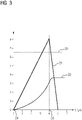
- figure 3 shows an exemplary course of the current intensity 31 in A, the supply voltage 32 and the output voltage 33 for such a test process.
- the supply voltage 32 is constant over the longer term and will be constant over the short period shown.
- the current does not rise directly to the maximum value through the inductance, but instead rises. This increase is generally non-linear. Since the current but in the short first period of time only reaches a small fraction of its maximum value, the increase in this time is practically linear. After the switch-off time, the current falls back to zero - also with a finite rate of current change.
- the output voltage also increases linearly during this time, with the value reached at the time of switch-off being small compared to the input voltage.
- t pulse designates the switch-on time, ie the first period of time.
- I peak is the current at the time of switch-off and U is the driving voltage.
- the size of the supply voltage 32 can be used as the driving voltage. This simplification represents only a small error as long as the output voltage that results during the first period of time remains small compared to the input voltage.
- the inductance can be determined with knowledge of the input voltage, the current strength at the switch-off time and the length of the first period of time.
- U in is the supply voltage
- U out0 is the output voltage present at the switch-on time
- U out1 is the output voltage present at the switch-off time.
- the values for the current strength and the output voltages resulting from the measurements depend on the supply voltage, the inductance and the selected period of time. In the case of certain combinations of these values, for example in the case of very high inductance or a very short period of time, the measured values are too small and therefore too imprecise to reliably determine the inductance.
- control device 25 is designed to compare the measured current intensity with a threshold value. If the current intensity falls below the threshold value, a new measurement is carried out, a second time period being used as the switch-on time, ie as the interval between the switch-on time and the switch-off time, which is longer than the first time period. For example, a time period of 6 ⁇ s can be used for the new measurement.
- control device 25 can be configured to increase the duty cycle used in steps of 2 ⁇ s, for example, until the measured current intensity exceeds the threshold value or until a maximum duty cycle is reached. If the current exceeds the threshold value, the measurement result can be used and the inductance of the supply lines can be determined. There the individual measurement is very short, even a large number of measurements require a time of less than 1 ms. Therefore, instead of a first time span of 4 ⁇ s, such a short first time span can be used, for example 500 ns, that only a very low current intensity is reached in any case. This ensures, even for unusual installation situations, that the test process does not cause any damage and in the subsequent longer measurements a current strength is then reached that allows the inductance to be determined.
- the result can be processed further, for example by electronically transmitting the determined inductance or by outputting it directly on a display.
- a comparison with values stored in the DC switch 20 for the maximum and minimum inductance for the supply lines 18 can also be carried out. If the inductance determined is between the minimum and maximum inductance, a signal can be output which corresponds to a positive message, for example by a green LED lighting up. Otherwise, a warning signal can be issued.
- the control device 25 can be designed to prevent the DC switch 20 from being switched on for active operation in the event of a negative result.
- the effective inductance is too high and operation is therefore not possible, or the input voltage is too low.
- the inductance can therefore not be determined, or can be determined only too imprecisely, and a warning signal can in turn be output and the switching on of the DC switch 20 can be prevented.
- control device 25 can be designed in certain specific embodiments of the DC switch 20 to repeat the measurement without changing the settings, in particular the duty cycle.
- the results collected and stored can then be averaged to reduce the influence of fluctuations in the measurement results.
- the measuring devices for determining the input and output voltage and current intensity are designed for the nominal values of the DC switch 20 and therefore deliver inaccurate results given the relatively low values that are reached during the test processes.
- control device 25 is further designed to carry out a second test process in the event that the inductance of the supply lines 18 is at least as great as the minimum inductance. Since the inductance of the supply lines 18 is sufficiently high, the shortest possible switch-on time no longer needs to be considered so intensively in order to avoid currents that are too high. Therefore, in the second test process, it is important to achieve a minimum current intensity in order to enable the inductance to be determined more precisely.
- the second test process therefore does not specify the duty cycle, but the current intensity.
- This specified current intensity can be selected in such a way that measurement inaccuracies only play a minor role.
- a current intensity can be calculated which is to be expected at the maximum inductance of the supply lines in a third period of time.
- This value is stored as a reference value in a comparison unit, for example a comparator. This also has the advantage that under certain circumstances the reference value can be set more precisely than the current measurement itself.
- the DC switch 20 is switched on for a maximum of the third period of time. If the current reaches the calculated value before the third period of time has elapsed, the DC switch 20 is switched off immediately and the elapsed on-time is stored. If the calculated value for the current is not reached, the current value reached is used as the result.
- the already introduced formula (2) can be applied. If the current reaches the calculated value before the end of the third period of time, the elapsed duty cycle is used as the value for the time t. Otherwise the determined maximum current value is used.
- control device 25 is configured to carry out the second test process without previously carrying out the first test process.
- the control device 25 is also designed to carry out a check of the connected capacity and a comparison with a stored maximum permissible pre-charging capacity. This is also limited, at least when using a pre-charging resistor. The value of the maximum permissible pre-charging capacity is stored in the control device 25 for this purpose.
- the resulting total amount of charge is the sum of the two parts, i.e. 20 pAs.
- a numerical integration method can also be used in a microcontroller in order to determine the amount of charge introduced. Then there is no need to divide it into two areas.
- the control device 25 determines whether it is permissible at all to switch on the pre-charging. For the positive and the negative case, the control device 25 can in turn be designed to output a signal electronically or to display it in a directly visible manner. Furthermore, the control device 25 can in turn be designed to prevent switching on if the maximum permissible pre-charging capacity is exceeded.
- the described DC switch 20 thus ensures non-destructively that the installed lead inductance is greater than the minimum permissible lead inductance and smaller than the maximum permissible. Furthermore, it also ensures that the installed load capacity is less than the maximum allowable pre-charge capacity. Advantageously, no complex manual measurements or tests are necessary for this.
- the DC switch 20 can also prevent switching on during operation if this would result in an unsafe operating state. It is also advantageously possible for the described test processes and the determination of the values connected on the load side to be carried out not only during commissioning but also during ongoing operation.
- the control device 25 can be designed to determine the connected inductance and/or capacitance before each switch-on process, which is required, for example, by a higher-level controller.
- the advantage here is that this determination takes only very little time, in particular less than 1 ms, even when carrying out a plurality of test processes with different time periods, and can therefore also be carried out during ongoing operation before switching on. If the permitted value ranges known to the DC switch 20 are not observed, the switch-on process does not take place and the DC switch 20 issues an error message.
Landscapes
- Physics & Mathematics (AREA)
- General Physics & Mathematics (AREA)
- Dc-Dc Converters (AREA)
- Control Of Voltage And Current In General (AREA)
- Electronic Switches (AREA)
- Power Conversion In General (AREA)
Priority Applications (3)
| Application Number | Priority Date | Filing Date | Title |
|---|---|---|---|
| EP20212658.7A EP4012926A1 (fr) | 2020-12-09 | 2020-12-09 | Commutateur à courant continu |
| CN202111477169.2A CN114614448A (zh) | 2020-12-09 | 2021-12-06 | 直流开关 |
| US17/545,953 US11601124B2 (en) | 2020-12-09 | 2021-12-08 | DC switch |
Applications Claiming Priority (1)
| Application Number | Priority Date | Filing Date | Title |
|---|---|---|---|
| EP20212658.7A EP4012926A1 (fr) | 2020-12-09 | 2020-12-09 | Commutateur à courant continu |
Publications (1)
| Publication Number | Publication Date |
|---|---|
| EP4012926A1 true EP4012926A1 (fr) | 2022-06-15 |
Family
ID=73789865
Family Applications (1)
| Application Number | Title | Priority Date | Filing Date |
|---|---|---|---|
| EP20212658.7A Pending EP4012926A1 (fr) | 2020-12-09 | 2020-12-09 | Commutateur à courant continu |
Country Status (3)
| Country | Link |
|---|---|
| US (1) | US11601124B2 (fr) |
| EP (1) | EP4012926A1 (fr) |
| CN (1) | CN114614448A (fr) |
Families Citing this family (1)
| Publication number | Priority date | Publication date | Assignee | Title |
|---|---|---|---|---|
| EP3654477A1 (fr) * | 2018-11-15 | 2020-05-20 | Siemens Aktiengesellschaft | Commutateur électronique à protection contre les surtensions |
Citations (5)
| Publication number | Priority date | Publication date | Assignee | Title |
|---|---|---|---|---|
| JP2002090402A (ja) * | 2000-09-20 | 2002-03-27 | Yokogawa Electric Corp | 容量測定装置 |
| EP1643256A1 (fr) * | 2004-09-30 | 2006-04-05 | Rockwell Automation Technologies, Inc. | Méthode et système pour la surveillance de l'impedance d'un ligne électrique pour courant alternatif |
| WO2017000996A1 (fr) * | 2015-06-30 | 2017-01-05 | Abb Schweiz Ag | Dispositif et procédé de mesure de capacité de câbles de puissance |
| CN106896275A (zh) * | 2017-02-13 | 2017-06-27 | 国网上海市电力公司 | 一种电缆分布电容风险预警控制系统 |
| US20200124657A1 (en) * | 2018-10-19 | 2020-04-23 | Taiyo Yuden Co., Ltd. | Reliability test device for coil |
Family Cites Families (6)
| Publication number | Priority date | Publication date | Assignee | Title |
|---|---|---|---|---|
| US20130043538A1 (en) * | 2011-08-16 | 2013-02-21 | Chao-Cheng Lu | Switch |
| DE202014011366U1 (de) * | 2014-08-28 | 2019-10-18 | Ellenberger & Poensgen Gmbh | Elektronischer Schutzschalter |
| JP6987774B2 (ja) * | 2016-03-14 | 2022-01-05 | ワイ−チャージ リミテッド | 光無線給電システム |
| WO2019038830A1 (fr) * | 2017-08-22 | 2019-02-28 | 東芝三菱電機産業システム株式会社 | Dispositif d'alimentation électrique |
| CN111971865B (zh) * | 2018-06-11 | 2022-12-06 | 西门子股份公司 | 固体断路器、用于固体断路器的断路方法 |
| CN113381386B (zh) * | 2020-03-10 | 2023-12-26 | 马克西姆综合产品公司 | 包括恒定功率控制器的电气开关系统及相关方法 |
-
2020
- 2020-12-09 EP EP20212658.7A patent/EP4012926A1/fr active Pending
-
2021
- 2021-12-06 CN CN202111477169.2A patent/CN114614448A/zh active Pending
- 2021-12-08 US US17/545,953 patent/US11601124B2/en active Active
Patent Citations (5)
| Publication number | Priority date | Publication date | Assignee | Title |
|---|---|---|---|---|
| JP2002090402A (ja) * | 2000-09-20 | 2002-03-27 | Yokogawa Electric Corp | 容量測定装置 |
| EP1643256A1 (fr) * | 2004-09-30 | 2006-04-05 | Rockwell Automation Technologies, Inc. | Méthode et système pour la surveillance de l'impedance d'un ligne électrique pour courant alternatif |
| WO2017000996A1 (fr) * | 2015-06-30 | 2017-01-05 | Abb Schweiz Ag | Dispositif et procédé de mesure de capacité de câbles de puissance |
| CN106896275A (zh) * | 2017-02-13 | 2017-06-27 | 国网上海市电力公司 | 一种电缆分布电容风险预警控制系统 |
| US20200124657A1 (en) * | 2018-10-19 | 2020-04-23 | Taiyo Yuden Co., Ltd. | Reliability test device for coil |
Also Published As
| Publication number | Publication date |
|---|---|
| US20220182051A1 (en) | 2022-06-09 |
| US11601124B2 (en) | 2023-03-07 |
| CN114614448A (zh) | 2022-06-10 |
Similar Documents
| Publication | Publication Date | Title |
|---|---|---|
| EP0666647B1 (fr) | Procédé et circuit pour commander des commutateurs semi-conducteurs montés en série | |
| DE102014105719A1 (de) | Schaltungsvorrichtung mit einer Thyristorschaltung sowie ein Verfahren zum Prüfen der Thyristorschaltung | |
| EP3887835B1 (fr) | Dispositif et procédé de vérification automatique d'un organe de commutation | |
| DE3609886A1 (de) | Daempfungsschaltung fuer gto-thyristor | |
| EP1801973B1 (fr) | Appareil de commande | |
| EP3754346A1 (fr) | Dispositif de détection, dispositif de commutation, système d'alimentation électrique, procédé de détection et procédé | |
| DE102021122687A1 (de) | Anordnung und Verfahren zur Entladung eines Zwischenkreiskondensators | |
| EP4012926A1 (fr) | Commutateur à courant continu | |
| EP3516701A1 (fr) | Module solaire, installation photovoltaïque et procédé de limitation de tension | |
| DE2326724C2 (de) | Trennfehler-Schutzschaltungsanordnung | |
| DE112016005736B4 (de) | Fahrzeugsteuervorrichtung | |
| DE4128679C1 (fr) | ||
| EP0970555A1 (fr) | Fusible electronique | |
| EP3314765B1 (fr) | Montage de circuits pour sortie de circuit numérique sûre et module de sortie ainsi que procédé de contrôle d'un tel montage de circuits | |
| EP1011190B1 (fr) | Méthode et circuit pour surveiller une charge en régime de fontionnement | |
| EP2876509B1 (fr) | Commande de sécurité | |
| WO2022073883A1 (fr) | Dispositif d'alimentation électrique et procédé de contrôle d'un transistor à effet de champ d'un tel dispositif d'alimentation électrique | |
| DE19913455A1 (de) | Kurzschlußschutz für Leistungshalbleiterschalter | |
| DE19546132C2 (de) | Schaltungsanordnung zum Schutz vor eingangsseitigem Überstrom bei Spannungszwischenkreisumrichtern | |
| DE2431167A1 (de) | Ueberwachungsschaltung fuer eine ueberlastschutzschaltung | |
| DE102021128811B3 (de) | Schaltungsanordnung mit zuverlässiger Erkennung von Kurzschlüssen | |
| EP3797408B1 (fr) | Dispositif, procédé et module de commande pour la surveillance d'une ligne à deux fils | |
| DE102008029679B4 (de) | System, Verfahren und elektronische Schaltung für mindestens eine elektronische Schaltungseinheit | |
| EP3916403A1 (fr) | Commutateur pour un réseau à tension continue et procédé de fonctionnement pour le commutateur | |
| DE102015220268A1 (de) | Vorrichtung und Verfahren zum Erkennen einer Fehlfunktion in einem Halbleiterschaltmodul |
Legal Events
| Date | Code | Title | Description |
|---|---|---|---|
| PUAI | Public reference made under article 153(3) epc to a published international application that has entered the european phase |
Free format text: ORIGINAL CODE: 0009012 |
|
| STAA | Information on the status of an ep patent application or granted ep patent |
Free format text: STATUS: THE APPLICATION HAS BEEN PUBLISHED |
|
| AK | Designated contracting states |
Kind code of ref document: A1 Designated state(s): AL AT BE BG CH CY CZ DE DK EE ES FI FR GB GR HR HU IE IS IT LI LT LU LV MC MK MT NL NO PL PT RO RS SE SI SK SM TR |
|
| STAA | Information on the status of an ep patent application or granted ep patent |
Free format text: STATUS: REQUEST FOR EXAMINATION WAS MADE |
|
| 17P | Request for examination filed |
Effective date: 20221118 |
|
| RBV | Designated contracting states (corrected) |
Designated state(s): AL AT BE BG CH CY CZ DE DK EE ES FI FR GB GR HR HU IE IS IT LI LT LU LV MC MK MT NL NO PL PT RO RS SE SI SK SM TR |