EP4012915A1 - Power conversion system - Google Patents
Power conversion system Download PDFInfo
- Publication number
- EP4012915A1 EP4012915A1 EP19940175.3A EP19940175A EP4012915A1 EP 4012915 A1 EP4012915 A1 EP 4012915A1 EP 19940175 A EP19940175 A EP 19940175A EP 4012915 A1 EP4012915 A1 EP 4012915A1
- Authority
- EP
- European Patent Office
- Prior art keywords
- filter
- power conversion
- circuit
- resistance
- reactor
- Prior art date
- Legal status (The legal status is an assumption and is not a legal conclusion. Google has not performed a legal analysis and makes no representation as to the accuracy of the status listed.)
- Pending
Links
Images


Classifications
-
- H—ELECTRICITY
- H02—GENERATION; CONVERSION OR DISTRIBUTION OF ELECTRIC POWER
- H02M—APPARATUS FOR CONVERSION BETWEEN AC AND AC, BETWEEN AC AND DC, OR BETWEEN DC AND DC, AND FOR USE WITH MAINS OR SIMILAR POWER SUPPLY SYSTEMS; CONVERSION OF DC OR AC INPUT POWER INTO SURGE OUTPUT POWER; CONTROL OR REGULATION THEREOF
- H02M7/00—Conversion of AC power input into DC power output; Conversion of DC power input into AC power output
- H02M7/42—Conversion of DC power input into AC power output without possibility of reversal
- H02M7/44—Conversion of DC power input into AC power output without possibility of reversal by static converters
- H02M7/48—Conversion of DC power input into AC power output without possibility of reversal by static converters using discharge tubes with control electrode or semiconductor devices with control electrode
- H02M7/493—Conversion of DC power input into AC power output without possibility of reversal by static converters using discharge tubes with control electrode or semiconductor devices with control electrode the static converters being arranged for operation in parallel
-
- H—ELECTRICITY
- H02—GENERATION; CONVERSION OR DISTRIBUTION OF ELECTRIC POWER
- H02J—ELECTRIC POWER NETWORKS; CIRCUIT ARRANGEMENTS OR SYSTEMS FOR SUPPLYING OR DISTRIBUTING ELECTRIC POWER; SYSTEMS FOR STORING ELECTRIC ENERGY
- H02J3/00—Circuit arrangements for AC mains or AC distribution networks
- H02J3/01—Arrangements for reducing harmonics or ripples
-
- H—ELECTRICITY
- H02—GENERATION; CONVERSION OR DISTRIBUTION OF ELECTRIC POWER
- H02M—APPARATUS FOR CONVERSION BETWEEN AC AND AC, BETWEEN AC AND DC, OR BETWEEN DC AND DC, AND FOR USE WITH MAINS OR SIMILAR POWER SUPPLY SYSTEMS; CONVERSION OF DC OR AC INPUT POWER INTO SURGE OUTPUT POWER; CONTROL OR REGULATION THEREOF
- H02M1/00—Details of apparatus for conversion
- H02M1/0003—Details of control, feedback or regulation circuits
-
- H—ELECTRICITY
- H02—GENERATION; CONVERSION OR DISTRIBUTION OF ELECTRIC POWER
- H02M—APPARATUS FOR CONVERSION BETWEEN AC AND AC, BETWEEN AC AND DC, OR BETWEEN DC AND DC, AND FOR USE WITH MAINS OR SIMILAR POWER SUPPLY SYSTEMS; CONVERSION OF DC OR AC INPUT POWER INTO SURGE OUTPUT POWER; CONTROL OR REGULATION THEREOF
- H02M1/00—Details of apparatus for conversion
- H02M1/12—Arrangements for reducing harmonics from AC input or output
- H02M1/126—Arrangements for reducing harmonics from AC input or output using passive filters
-
- H—ELECTRICITY
- H02—GENERATION; CONVERSION OR DISTRIBUTION OF ELECTRIC POWER
- H02M—APPARATUS FOR CONVERSION BETWEEN AC AND AC, BETWEEN AC AND DC, OR BETWEEN DC AND DC, AND FOR USE WITH MAINS OR SIMILAR POWER SUPPLY SYSTEMS; CONVERSION OF DC OR AC INPUT POWER INTO SURGE OUTPUT POWER; CONTROL OR REGULATION THEREOF
- H02M7/00—Conversion of AC power input into DC power output; Conversion of DC power input into AC power output
- H02M7/42—Conversion of DC power input into AC power output without possibility of reversal
- H02M7/44—Conversion of DC power input into AC power output without possibility of reversal by static converters
- H02M7/48—Conversion of DC power input into AC power output without possibility of reversal by static converters using discharge tubes with control electrode or semiconductor devices with control electrode
- H02M7/4803—Conversion of DC power input into AC power output without possibility of reversal by static converters using discharge tubes with control electrode or semiconductor devices with control electrode with means for reducing DC component from AC output voltage
-
- H—ELECTRICITY
- H02—GENERATION; CONVERSION OR DISTRIBUTION OF ELECTRIC POWER
- H02J—ELECTRIC POWER NETWORKS; CIRCUIT ARRANGEMENTS OR SYSTEMS FOR SUPPLYING OR DISTRIBUTING ELECTRIC POWER; SYSTEMS FOR STORING ELECTRIC ENERGY
- H02J2101/00—Supply or distribution of decentralised, dispersed or local electric power generation
- H02J2101/20—Dispersed power generation using renewable energy sources
- H02J2101/28—Wind energy
-
- H—ELECTRICITY
- H02—GENERATION; CONVERSION OR DISTRIBUTION OF ELECTRIC POWER
- H02J—ELECTRIC POWER NETWORKS; CIRCUIT ARRANGEMENTS OR SYSTEMS FOR SUPPLYING OR DISTRIBUTING ELECTRIC POWER; SYSTEMS FOR STORING ELECTRIC ENERGY
- H02J3/00—Circuit arrangements for AC mains or AC distribution networks
- H02J3/38—Arrangements for feeding a single network from two or more generators or sources in parallel; Arrangements for feeding already energised networks from additional generators or sources in parallel
- H02J3/381—Dispersed generators
-
- H—ELECTRICITY
- H03—ELECTRONIC CIRCUITRY
- H03H—IMPEDANCE NETWORKS, e.g. RESONANT CIRCUITS; RESONATORS
- H03H7/00—Multiple-port networks comprising only passive electrical elements as network components
- H03H7/01—Frequency selective two-port networks
- H03H7/09—Filters comprising mutual inductance
-
- Y—GENERAL TAGGING OF NEW TECHNOLOGICAL DEVELOPMENTS; GENERAL TAGGING OF CROSS-SECTIONAL TECHNOLOGIES SPANNING OVER SEVERAL SECTIONS OF THE IPC; TECHNICAL SUBJECTS COVERED BY FORMER USPC CROSS-REFERENCE ART COLLECTIONS [XRACs] AND DIGESTS
- Y02—TECHNOLOGIES OR APPLICATIONS FOR MITIGATION OR ADAPTATION AGAINST CLIMATE CHANGE
- Y02E—REDUCTION OF GREENHOUSE GAS [GHG] EMISSIONS, RELATED TO ENERGY GENERATION, TRANSMISSION OR DISTRIBUTION
- Y02E40/00—Technologies for an efficient electrical power generation, transmission or distribution
- Y02E40/40—Arrangements for reducing harmonics
Definitions
- the present application relates to a power conversion system.
- each of the plurality of power conversion devices includes a power conversion circuit, and an AC filter circuit connected to the output side of the power conversion circuit.
- the AC filter circuit includes an AC filter reactor and an AC filter capacitor.
- LC low-pass filters have various circuitry types including an L type, a T type, and a II (pi) type. With respect to such a point, it is clearly described in paragraph 0017 of the above-mentioned JP 2014-183601 A that an AC filter for removing high frequency voltage components may be a T-type filter.
- the AC filter circuit is required to have both passing performance, which allows a fundamental wave current to pass therethrough, and damping performance, which filters high frequency components, such as a ripple current.
- passing performance which allows a fundamental wave current to pass therethrough
- damping performance which filters high frequency components, such as a ripple current.
- circuit components having as small a size as possible There is a demand to ideally realize such performances with circuit components having as small a size as possible.
- a power conversion system in which a plurality of power conversion devices are connected in parallel has a further matter which should be taken into consideration.
- an electric current may be generated between one power conversion device and another power conversion device due to resonance of AC filter circuit elements.
- this electric current due to resonance is also referred to as "resonant current”.
- the present application is directed to a power conversion system including a plurality of power conversion devices connected in parallel, each of the plurality of power conversion devices including:
- the second filter reactor is connected in series to the AC filter capacitor of the L-type LC low-pass filter.
- a fundamental wave current does not flow into the second filter reactor so that even a reactor having a small size can satisfy required performance. Therefore, it is possible to achieve a reduction in size of constitutional components of the AC filter circuit while required performance of the AC filter circuit is satisfied.
- the resistance provided to the AC filter circuit acts as a damping element. Accordingly, it is possible to achieve both a reduction in size of the AC filter circuit and suppression of a resonant current.
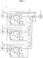
- Fig. 1 is a system configuration diagram of a power conversion system 1 according to an embodiment.
- the power conversion system 1 is a grid interconnection system including a plurality of power conversion devices 4 connected in parallel. The respective output sides of the plurality of power conversion devices 4 are joined via a parallel junction P.
- An upper transformer 3 is provided between the parallel junction P and a power system 2.
- Each of the plurality of power conversion devices 4 includes a power conversion circuit 4a, which converts DC to AC, and an AC filter circuit 4b, which is connected to the output side of the power conversion circuit 4a.
- One example of the power conversion circuit 4a according to the embodiment is a voltage controlled three-phase inverter circuit.
- the input side of each of the plurality of power conversion devices 4 is provided with a distributed power supply 5.
- the distributed power supply 5 is a DC power supply.
- the power conversion device 4 converts DC power from the distributed power supply 5 to AC power, and outputs the AC power toward the power system 2 side.
- the distributed power supply 5 may be a power generation facility or a battery facility.
- the battery facility may be a storage battery facility including a secondary battery capable of controlling charging and discharging (that is, a storage battery).
- the battery facility may be a fuel cell facility which causes electric power to be generated from chemical energy of fuel by an electrochemical reaction.
- the power generation facility may be a so-called renewable energy generation facility.
- the renewable energy generation facility may be a photovoltaic power generation facility.
- the renewable energy generation facility may be a wind power generation facility which includes a wind power generator and a converter device which converts the output from this wind power generator to DC power.
- the plurality of distributed power supplies 5 included by the power conversion system 1 may be power supplies of the same kind.
- the plurality of distributed power supplies 5 may be power supplies of different kinds.
- some of the distributed power supply 5 may be power supplies of a first kind from the above-mentioned various power supplies, and the remaining distributed power supplies 5 may be power supplies of a second kind from the above-mentioned various power supplies.
- Each AC filter circuit 4b includes a first filter reactor L 1 , an AC filter capacitor C 1 , a second filter reactor L 2 , and a resistance R.
- the AC filter circuit 4b is an LC low-pass filter where the first filter reactor L 1 and the AC filter capacitor C 1 are connected in an L shape.
- the second filter reactor L 2 is connected in series to the AC filter capacitor C 1 .
- the resistance R constructs a series circuit together with the AC filter capacitor C 1 and the second filter reactor L 2 .
- one end of the first filter reactor L 1 is connected to the output side of the power conversion circuit 4a.
- the other end of the first filter reactor L 1 is connected to one end of the resistance R.
- One end of the second filter reactor L 2 is connected to the other end of the resistance R.
- the other end of the second filter reactor L 2 is connected to one end of the AC filter capacitor C 1 .
- the resistance R, the second filter reactor L 2 and the AC filter capacitor C 1 are connected in series in that order so that an RLC series circuit is constituted.
- an interconnection reactor, an interconnection transformer or the like is not provided between the parallel junction P and the AC filter circuit 4b. This is because the resistance R functions as a damping resistance R in the embodiment so that components of the damping element, such as the interconnection reactor, may be omitted. As a result, it is possible to reduce the number of components.
- the power conversion system 1 in which the plurality of power conversion devices 4 are connected in parallel as in the case of the embodiment has an advantage that the power conversion system 1 can handle large electric power while individual power conversion devices 4 is allowed to have a small capacity or a medium capacity. Even if there is an increase in the number of power conversion devices 4, each of which has a small capacity or a medium capacity, and which are connected in parallel, there may be a case where cost advantage and the like can be obtained compared with the case where one or a small number of power conversion devices 4 having a large capacity are disposed.
- a fundamental wave current I 1 is a main electric current of AC to be outputted from the power conversion circuit 4a.
- the ripple current I 2 is a high frequency current which is generated with switching of the power conversion circuit 4a.
- an electric current may be generated between one power conversion device and another power conversion device due to resonance of elements of the AC filter circuits. This electric current due to resonance is referred to as "resonant current I 3 " for the sake of convenience.
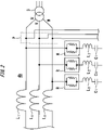
- Fig. 2 is a diagram for describing the AC filter circuit 4b of the power conversion system 1 according to the embodiment.
- Fig. 2 is a diagram for describing the configuration of the AC filter circuit 4b in a three-phase AC system.
- the power conversion circuit 4a forms a three-phase inverter circuit so that each of UVW three-phase connections is provided with the AC filter circuit 4b.
- the three-phase connections shown in Fig. 2 are reduced to one-phase connection or two-phase connection.
- the AC filter circuit 4b corresponding to the number of reduced connections may be omitted.
- each second filter reactor L 2 is connected in series to the AC filter capacitor C 1 of the L-type LC low-pass filter.
- the fundamental wave current I 1 does not flow into the second filter reactor L 2 so that even a reactor having a small size can satisfy required performance. Therefore, it is possible to achieve a reduction in size of the inductance component and the capacitance component which construct the AC filter circuit 4b while required performance of filtering the ripple current I 2 is sufficiently ensured.
- the resistance R provided to the AC filter circuit 4b acts as a damping element and hence, even when an L-type LC low-pass filter is used, the resonant current I 3 between the plurality of power conversion devices 4 can be suppressed. Accordingly, it is possible to achieve both a reduction in size of the AC filter circuit 4b and suppression of the resonant current I 3 .
- Using a circuit component having a small size also reduces costs.
- Fig. 3 is a graph for describing a frequency characteristic of the AC filter circuit 4b of the power conversion system 1 according to the embodiment.
- a gain characteristic A1 of the AC filter circuit 4b is illustrated.
- the gain characteristic A1 includes a low-frequency portion pa1, a local maximum pa2, an intermediate portion pa3, a local minimum pa4, an inflection point pa5, and a high-frequency portion pa6.
- the low-frequency portion pa1 is a portion which is provided on a low frequency side, and in which the gain gradually decreases corresponding to an increase in frequency.
- the local maximum pa2 is a portion which is present on the high frequency side of the low-frequency portion pa1, and which is sharpened upward in the graph.
- the intermediate portion pa3 is a portion which is present on the high frequency side of the local maximum pa2, and in which the gain rapidly falls corresponding to an increase in frequency.
- the local minimum pa4 is the lower end of the intermediate portion pa3.
- the inflection point pa5 is a point where a change rate of the gain characteristic changes from a positive to a negative after a rapid rise from the local minimum pa4.
- the high-frequency portion pa6 is a portion which is present on the high frequency side of the inflection point pa5, and in which the gain gradually decreases corresponding to an increase in frequency.
- Fig. 3 describes a first frequency f1, which corresponds to the local maximum pa2, and a second frequency f2, which corresponds to the local minimum pa4.
- the second frequency f2 is determined by a resonance frequency fo of an LC series circuit which is formed of the second filter reactor L 2 and the AC filter capacitor C 1 .
- the resonance frequency fo is determined based on the inductance value of the second filter reactor L 2 and the capacitance value of the AC filter capacitor C 1 .
- the resonance frequency fo be equal to a carrier frequency fc in the power conversion circuit 4a.
- the carrier frequency fc is a frequency which is determined corresponding to switching control parameters of the power conversion circuit 4a.
- Fig. 4 is a system configuration diagram of a power conversion system 1 according to the comparison example.
- Fig. 5 and Fig. 6 are graphs for describing a frequency characteristic of an AC filter circuit 40b according to the comparison example.
- Fig. 5 and Fig. 6 show a gain characteristic B1 of the AC filter circuit 40b, and also show a local maximum pb1 of the gain characteristic B1.
- the AC filter circuit 40b is a T-type LC low-pass filter.
- the T-type LC low-pass filter is an LCL low-pass filter where a reactor and a capacitor are connected in the order of LCL.
- the AC filter circuit 40b according to the comparison example has the following defects.
- the fundamental wave current I 1 of the power conversion circuit 4a and the ripple current I 2 which is generated with switching of the power conversion circuit 4a pass through a first filter reactor L 11 . Therefore, the first filter reactor L 11 has a large volume.
- the volume of the iron core of the second filter reactor L 12 is smaller than the volume of the iron core of the first filter reactor L 11 .
- the winding wire of the second filter reactor L 12 is required to have a crosssectional area which corresponds to that of the winding wire of the first filter reactor L 11 .
- An AC filter capacitor C 0 absorbs the ripple current I 2 which is generated with switching of the power conversion circuit 4a. Therefore, the AC filter capacitor C 0 is required to have a capacitance value which is several % of the capacity of the power conversion device 4. Further, from the viewpoint of a control, it is necessary to compensate the capacity of the AC filter capacitor at the AC output end of the power conversion circuit 4a so that there is also a defect that excess reactive power is outputted.
- the second filter reactor L 2 and the AC filter capacitor C 1 are selected such that the resonance frequency fo assumes a value which corresponds to the carrier frequency fc of the power conversion circuit 4a.
- gains have the same value (that is -35dB) at the same carrier frequency fc, so that substantially the same filter performance can be acquired.
- the inductance value of the first filter reactor L 11 of the comparison example which realizes the characteristic shown in Fig. 5 is larger than the first filter reactor L 1 of the embodiment by approximately 1.33 times.
- the capacitance value of the AC filter capacitor C 0 of the comparison example which realizes the characteristic shown in Fig. 5 is larger than the AC filter capacitor C 1 of the embodiment by approximately 6 times.
- the AC filter circuit 40b according to the comparison example has a problem that a size of the constitutional components becomes larger than that of the AC filter circuit 4 according to the embodiment.
- the inductance value of the first filter reactor L 1 can be reduced to approximately 1/1.33 of the inductance value of the first filter reactor L 11 .
- the ripple current I 2 is sufficiently smaller than the fundamental wave current I 1 so that it is possible to have an advantage that the second filter reactor L 2 has a small volume.
- the capacitance value of the AC filter capacitor C 1 can also be reduced to approximately 1/6 of the AC filter capacitor C 0 . Therefore, it is possible to use a small-sized capacitor as the AC filter capacitor C 1 . With the use of the small-sized circuit components as described above, it is possible to expect a cost reduction effect brought about by a reduction in the volume of the components, and it is also possible to expect a cost reduction effect brought about by a reduction in the number of circuit components.
- substantially the same filter performance can be created using components having the lower inductance and the lower capacitance than those of the AC filter circuit 40b of the comparison example, which is a T-type LC low-pass filter.
- the AC filter circuit 4b does not include the second filter reactor L 12 which is provided on the downstream side of the first filter reactor L 11 , and which is included in the T-type LC low-pass filter of the comparison example.
- the second filter reactor L 12 provided on the downstream side of the first filter reactor L 11 cannot be caused to act as a damping element.
- the resistance R which is added to the AC filter circuit 4b acts as the damping element and hence, it is possible to suppress the resonant current I 3 which flows on the output side of the plurality of power conversion devices 4.
- the resistance R which acts as the damping element is provided for reducing the resonant current I 3 which flows between power conversion devices 4 arranged in parallel so that the resistance component having a large size may not be used. Therefore, it is possible to achieve both a reduction in size of the AC filter circuit 4b and suppression of the resonant current I 3 . Further, for a control, the capacity of the AC filter capacitor C 1 can be reduced and hence, there is an advantage that compensating reactive power can also be reduced.
- Fig. 6 is a second frequency characteristic graph relating to the comparison example.
- Fig. 6 shows a frequency characteristic in the case where the first filter reactor L 11 is caused to have the same inductance value as the first filter reactor L 1 , and the AC filter capacitor C 0 is caused to have the same capacitance value as the AC filter capacitor C 1 .
- the gain at the carrier frequency fc is near -5dB, so filter performance is deteriorated compared with the graph of the embodiment shown in Fig. 3 .
- the inductance value of the first filter reactor L 1 can be reduced to 1/1.33 of the inductance value in the comparison example, and the capacitance value of the AC filter capacitor C 1 can be reduced to 1/6 of the capacitance value in the comparison example.
- the resonance frequency fo is positioned somewhere near the carrier frequency fc.
- the resistance R may be a large current resistance which allows a flow of a large current. However, it is not preferable to provide a larger resistance than necessary. For example, in the case where the magnitude of the ripple current I 2 is 1/10 or less of the magnitude of the fundamental wave current I 1 , it is sufficient for the resistance R to have the current resistance specification of a degree that the resistance R can withstand a flow of an electric current of 1/10 or less of the fundamental wave current I 1 . It is preferable that the resistance R be constructed to suppress heat to be generated when the ripple current I 2 flows. For example, the resistance R may be constructed to have a structure where the amount of heat generation with respect to an electric current is suppressed. The resistance R may be a resistance component to which a heat radiation unit or a cooling unit is provided.
- the resistance R may be constructed by connecting a plurality of resistance components in parallel.
- the resistance R may be constructed by only one resistance component.
- the resistance R may be constructed by connecting a plurality of resistance components in series or in seriesparallel.
- the resistance R may be a non-inductive resistor.
- the non-inductive resistor is a resistor where parasitic inductance is significantly suppressed.
- the non-inductive resistor is formed by a winding method referred to as "non-induction winding".
- the "non-induction winding” is a structure where two resistance wires are wound in opposite winding directions. Provided that the two resistance wires have the same number of turns, and the same amount of electric current flowing therethrough, magnetic fields to be generated in the two resistance wires have the same magnitude but opposite directions. As a result, the magnetic fields cancel each other out so that the inductance can be reduced.
- non-inductive resistor As one example of the non-inductive resistor, a known resistance disclosed in JP 2010-109256 A or the like, for example, may also be used.
- the non-inductive resistor is constituted not to release inductive components during energization (not to have inductance).
- Non-inductive resistors of this kind include a non-inductive resistor of a wire wound type and a non-inductive resistor of a solid type.
- the non-inductive resistor of the wire wound type may be constructed to be energized such that "a winding direction of one winding wire” and "a winding direction of an adjacent winding wire” are made opposite to each other so that a magnetic field (magnetic flux) generated by the above-mentioned one winding wire and a magnetic field (magnetic flux) generated by the adjacent winding wire cancel each other out.
- the non-inductive resistor of the wire wound type may also be constructed to be energized such that "a winding direction of a winding wire in one zone" and "a winding direction of a winding wire in an adjacent zone” are made opposite to each other so that a magnetic field (magnetic flux) generated by the winding wire in the one zone and a magnetic field (magnetic flux) generated by the winding wire in the adjacent zone cancel each other out.
- inductive components can be reduced so that actual inductance can be reduced to an extremely small value.
- the non-inductive resistor of the solid type is constructed such that a solid per se, such as a carbon film or a metal film, forming a resistor has a cylindrical shape or a wide thin shape. With such a configuration, the inductive components can be reduced.
- the non-inductive resistor may be a non-inductive resistor obtained by folding back and winding a resistance wire, or a non-inductive resistor obtained by forming a resistance film on a planar insulator in a zigzag manner.
- a wire wound resistor, a carbon film resistor, a metal film resistor, a solid resistor, a chip resistor, and other resistors are put into practice as solid resistors.
- a resistor having sufficiently smaller inductance than a general resistor is referred to as "non-inductive resistor" and is used as a non-inductive resistor. Therefore, a solid resistor and a chip resistor which do not generally form a coil-shaped electric path may be treated as the non-inductive resistor.
- non-inductive resistor As still another example of the non-inductive resistor, a known resistance disclosed in JP H6-32642 U or the like may also be used. As a non-inductive resistor having a round rod shape, a metal resistance, a ceramic resistance or the like may also be used. Further, as a non-inductive resistor having a flat shape, a metal thin-film resistance, an Ayrton-Perry winding resistance or the like may also be used.
- the resistance R may be a plate-shaped resistor.
- a known plate-shaped resistor disclosed in JP 2010-287842 A or the like may also be used.
- a high-power non-inductive resistor may also be used where a resistor includes a plate-shaped resistance portion having electrode portions at both ends thereof, an insulating plate which insulates this resistor, and a heat radiation plate are stacked.
- the insulating plate may be a pair of ceramic substrates which are respectively stacked on both surfaces of the resistance portion of the resistor.
- the resistor is not limited to the above, and any of various large current resistors may also be used as the resistance R.
- a known resistance disclosed in JP 2017-162948 A or the like may also be used.
- a cement resistor or a vitreous enamel resistor may also be used.
- the cement resistor may be a resistor formed such that a wire wound resistance unit or a metal oxide film resistance unit is put into a casing made of ceramic, and the casing is sealed by a silicon based resin (cement).
- the vitreous enamel resistor may be a resistor formed such that a resistance wire is wound around a bobbin made of porcelain, and is coated by vitreous enamel.
- a known resistance disclosed in JP 2002-175901 A or the like may also be used.
- a power converter such as an inverter or a power module on which an IGBT element and the like are mounted
- an electric resistor with high accuracy of approximately 0.1 m ⁇ to 100 m ⁇ is used to accurately detect a large current ranging from approximately several A to 400 A.
- the power converter allows a large current so that large electric power is generated in a resistor whereby it is necessary to radiate heat.
- a resistor may also be used which has a structure where a plurality of resistance alloy sheets and a plurality of heat radiation metal sheets are stacked with resin insulating layers interposed therebetween.
- a copper-manganese-based alloy, a copper-manganese-nickel-based alloy, or a copper-nickel-based alloy having a large resistance ratio may also be used as a resistance alloy.
- An example of such a copper-manganese-nickel-based alloy may be Manganin.
- a copper-nickel-based alloy may be an alloy which contains a small amount of Mn, Fe, and Si in addition to constantan and the like.
- the resistance value of the resistance R may be 10 m ⁇ or less, for example.
- the resistance value of the resistance R may be 1 m ⁇ to 20 m ⁇ , may be 1 m ⁇ to 15 m ⁇ , or may be 1 m ⁇ to 10 m ⁇ .
- the resistance value of the resistance R may be 5 m ⁇ to 20 m ⁇ , may be 10 m ⁇ to 20 m ⁇ , or may be 15 m ⁇ to 20 m ⁇ .
- the resistance value of the resistance R may be 5 m ⁇ to 15 m ⁇ , or 5 m ⁇ to 10 m ⁇ .
Landscapes
- Engineering & Computer Science (AREA)
- Power Engineering (AREA)
- Inverter Devices (AREA)
- Power Conversion In General (AREA)
Abstract
Description
- The present application relates to a power conversion system.
- As disclosed in
JP 2014-183601 A Fig. 2 , for example, ofJP 2014-183601 A - Known LC low-pass filters have various circuitry types including an L type, a T type, and a II (pi) type. With respect to such a point, it is clearly described in paragraph 0017 of the above-mentioned
JP 2014-183601 A - [PTL 1]
JP 2014-183601 A - The AC filter circuit is required to have both passing performance, which allows a fundamental wave current to pass therethrough, and damping performance, which filters high frequency components, such as a ripple current. There is a demand to ideally realize such performances with circuit components having as small a size as possible. However, a power conversion system in which a plurality of power conversion devices are connected in parallel has a further matter which should be taken into consideration. In the case where the plurality of power conversion devices are connected in parallel, an electric current may be generated between one power conversion device and another power conversion device due to resonance of AC filter circuit elements. Hereinafter, this electric current due to resonance is also referred to as "resonant current".
- From the viewpoint of suppressing the above-mentioned resonant current, as in the case of a T-type LC low-pass filter, it is preferable to provide an AC filter reactor on the downstream side of an AC filter capacitor. This is because this AC filter reactor provided on the downstream side acts as a so-called damping element. However, the AC filter reactor provided on the downstream side of the AC filter capacitor is required to allow a fundamental wave current to flow therethrough, thus being required to be a component having a certain size. As a result, the T-type LC low-pass filter has a problem that a reduction in size of the AC filter circuit is difficult.
- It is an object of the present application to provide a power conversion system which can achieve both a reduction in size of the AC filter circuit and suppression of a resonant current.
- The present application is directed to a power conversion system including a plurality of power conversion devices connected in parallel,
each of the plurality of power conversion devices including: - a power conversion circuit configured to convert DC to AC; and
- an AC filter circuit connected to an output side of the power conversion circuit,
- the AC filter circuit being an LC low-pass filter including a first filter reactor and an AC filter capacitor connected in an L shape, and
- the AC filter circuit further including a second filter reactor connected in series to the AC filter capacitor, and a resistance constructing a series circuit together with the AC filter capacitor and the second filter reactor.
- According to the power conversion system of the present application, the second filter reactor is connected in series to the AC filter capacitor of the L-type LC low-pass filter. A fundamental wave current does not flow into the second filter reactor so that even a reactor having a small size can satisfy required performance. Therefore, it is possible to achieve a reduction in size of constitutional components of the AC filter circuit while required performance of the AC filter circuit is satisfied. Further, the resistance provided to the AC filter circuit acts as a damping element. Accordingly, it is possible to achieve both a reduction in size of the AC filter circuit and suppression of a resonant current.
-
- [
Fig. 1 ]
Fig. 1 is a system configuration diagram of a power conversion system according to an embodiment. - [
Fig. 2 ]
Fig. 2 is a diagram for describing AC filter circuits of the power conversion system according to the embodiment. - [
Fig. 3 ]
Fig. 3 is a graph for describing a frequency characteristic of the AC filter circuit of the power conversion system according to the embodiment. - [
Fig. 4 ]
Fig. 4 is a system configuration diagram of a power conversion system according to a comparison example. - [
Fig. 5 ]
Fig. 5 is a graph for describing a frequency characteristic of an AC filter circuit according to the comparison example. - [
Fig. 6 ]
Fig. 6 is a graph for describing a frequency characteristic of an AC filter circuit according to a comparison example. -
Fig. 1 is a system configuration diagram of apower conversion system 1 according to an embodiment. As shown inFig. 1 , thepower conversion system 1 is a grid interconnection system including a plurality ofpower conversion devices 4 connected in parallel. The respective output sides of the plurality ofpower conversion devices 4 are joined via a parallel junction P. Anupper transformer 3 is provided between the parallel junction P and apower system 2. - Each of the plurality of
power conversion devices 4 includes apower conversion circuit 4a, which converts DC to AC, and anAC filter circuit 4b, which is connected to the output side of thepower conversion circuit 4a. One example of thepower conversion circuit 4a according to the embodiment is a voltage controlled three-phase inverter circuit. - The input side of each of the plurality of
power conversion devices 4 is provided with adistributed power supply 5. Thedistributed power supply 5 is a DC power supply. Thepower conversion device 4 converts DC power from thedistributed power supply 5 to AC power, and outputs the AC power toward thepower system 2 side. - For the
distributed power supply 5, any of the following various power supplies may be suitably used. For example, thedistributed power supply 5 may be a power generation facility or a battery facility. For example, the battery facility may be a storage battery facility including a secondary battery capable of controlling charging and discharging (that is, a storage battery). For example, the battery facility may be a fuel cell facility which causes electric power to be generated from chemical energy of fuel by an electrochemical reaction. For example, the power generation facility may be a so-called renewable energy generation facility. The renewable energy generation facility may be a photovoltaic power generation facility. Alternatively, the renewable energy generation facility may be a wind power generation facility which includes a wind power generator and a converter device which converts the output from this wind power generator to DC power. - The plurality of
distributed power supplies 5 included by thepower conversion system 1 may be power supplies of the same kind. Alternatively, the plurality ofdistributed power supplies 5 may be power supplies of different kinds. In other words, some of the distributedpower supply 5 may be power supplies of a first kind from the above-mentioned various power supplies, and the remaining distributedpower supplies 5 may be power supplies of a second kind from the above-mentioned various power supplies. - Each
AC filter circuit 4b includes a first filter reactor L1, an AC filter capacitor C1, a second filter reactor L2, and a resistance R. TheAC filter circuit 4b is an LC low-pass filter where the first filter reactor L1 and the AC filter capacitor C1 are connected in an L shape. The second filter reactor L2 is connected in series to the AC filter capacitor C1. The resistance R constructs a series circuit together with the AC filter capacitor C1 and the second filter reactor L2. - Specifically, one end of the first filter reactor L1 is connected to the output side of the
power conversion circuit 4a. The other end of the first filter reactor L1 is connected to one end of the resistance R. One end of the second filter reactor L2 is connected to the other end of the resistance R. The other end of the second filter reactor L2 is connected to one end of the AC filter capacitor C1. The resistance R, the second filter reactor L2 and the AC filter capacitor C1 are connected in series in that order so that an RLC series circuit is constituted. - In the embodiment, an interconnection reactor, an interconnection transformer or the like is not provided between the parallel junction P and the
AC filter circuit 4b. This is because the resistance R functions as a damping resistance R in the embodiment so that components of the damping element, such as the interconnection reactor, may be omitted. As a result, it is possible to reduce the number of components. - The
power conversion system 1 in which the plurality ofpower conversion devices 4 are connected in parallel as in the case of the embodiment has an advantage that thepower conversion system 1 can handle large electric power while individualpower conversion devices 4 is allowed to have a small capacity or a medium capacity. Even if there is an increase in the number ofpower conversion devices 4, each of which has a small capacity or a medium capacity, and which are connected in parallel, there may be a case where cost advantage and the like can be obtained compared with the case where one or a small number ofpower conversion devices 4 having a large capacity are disposed. - In
Fig. 1 , a fundamental wave current I1, a ripple current I2, and a resonant current I3 are illustrated as electric currents which flow through thepower conversion system 1. The fundamental wave current I1 is a main electric current of AC to be outputted from thepower conversion circuit 4a. The ripple current I2 is a high frequency current which is generated with switching of thepower conversion circuit 4a. In the case where the plurality of power conversion devices are connected in parallel, an electric current may be generated between one power conversion device and another power conversion device due to resonance of elements of the AC filter circuits. This electric current due to resonance is referred to as "resonant current I3" for the sake of convenience. -
Fig. 2 is a diagram for describing theAC filter circuit 4b of thepower conversion system 1 according to the embodiment.Fig. 2 is a diagram for describing the configuration of theAC filter circuit 4b in a three-phase AC system. In the embodiment, thepower conversion circuit 4a forms a three-phase inverter circuit so that each of UVW three-phase connections is provided with theAC filter circuit 4b. However, in the case where thepower conversion circuit 4a forms a single-phase or two-phase inverter circuit or the like as a modification, the three-phase connections shown inFig. 2 are reduced to one-phase connection or two-phase connection. In this case, theAC filter circuit 4b corresponding to the number of reduced connections may be omitted. - According to the above-mentioned
power conversion system 1, each second filter reactor L2 is connected in series to the AC filter capacitor C1 of the L-type LC low-pass filter. The fundamental wave current I1 does not flow into the second filter reactor L2 so that even a reactor having a small size can satisfy required performance. Therefore, it is possible to achieve a reduction in size of the inductance component and the capacitance component which construct theAC filter circuit 4b while required performance of filtering the ripple current I2 is sufficiently ensured. Whereas the resistance R provided to theAC filter circuit 4b acts as a damping element and hence, even when an L-type LC low-pass filter is used, the resonant current I3 between the plurality ofpower conversion devices 4 can be suppressed. Accordingly, it is possible to achieve both a reduction in size of theAC filter circuit 4b and suppression of the resonant current I3. Using a circuit component having a small size also reduces costs. -
Fig. 3 is a graph for describing a frequency characteristic of theAC filter circuit 4b of thepower conversion system 1 according to the embodiment. In the graph of the frequency characteristic shown inFig. 3 , a gain characteristic A1 of theAC filter circuit 4b is illustrated. The gain characteristic A1 includes a low-frequency portion pa1, a local maximum pa2, an intermediate portion pa3, a local minimum pa4, an inflection point pa5, and a high-frequency portion pa6. - The low-frequency portion pa1 is a portion which is provided on a low frequency side, and in which the gain gradually decreases corresponding to an increase in frequency. The local maximum pa2 is a portion which is present on the high frequency side of the low-frequency portion pa1, and which is sharpened upward in the graph. The intermediate portion pa3 is a portion which is present on the high frequency side of the local maximum pa2, and in which the gain rapidly falls corresponding to an increase in frequency. The local minimum pa4 is the lower end of the intermediate portion pa3. The inflection point pa5 is a point where a change rate of the gain characteristic changes from a positive to a negative after a rapid rise from the local minimum pa4. The high-frequency portion pa6 is a portion which is present on the high frequency side of the inflection point pa5, and in which the gain gradually decreases corresponding to an increase in frequency.
-
Fig. 3 describes a first frequency f1, which corresponds to the local maximum pa2, and a second frequency f2, which corresponds to the local minimum pa4. The second frequency f2 is determined by a resonance frequency fo of an LC series circuit which is formed of the second filter reactor L2 and the AC filter capacitor C1. The resonance frequency fo is determined based on the inductance value of the second filter reactor L2 and the capacitance value of the AC filter capacitor C1. - It is preferable that the resonance frequency fo be equal to a carrier frequency fc in the
power conversion circuit 4a. The carrier frequency fc is a frequency which is determined corresponding to switching control parameters of thepower conversion circuit 4a. When the resonance frequency fo and the carrier frequency fc are made equal to each other, in the L-type LC low-pass filter which uses components having a low inductance and a low capacitance, it is possible to ensure the gain equivalent to that of a T-type LC low-pass AC filter circuit. - Advantageous effects of the embodiment will be described with reference to comparison examples shown in
Fig. 4 to Fig. 6 .Fig. 4 is a system configuration diagram of apower conversion system 1 according to the comparison example.Fig. 5 andFig. 6 are graphs for describing a frequency characteristic of anAC filter circuit 40b according to the comparison example.Fig. 5 andFig. 6 show a gain characteristic B1 of theAC filter circuit 40b, and also show a local maximum pb1 of the gain characteristic B1. - In the comparison example shown in
Fig. 4 , theAC filter circuit 40b is a T-type LC low-pass filter. In other words, the T-type LC low-pass filter is an LCL low-pass filter where a reactor and a capacitor are connected in the order of LCL. - The
AC filter circuit 40b according to the comparison example has the following defects. The fundamental wave current I1 of thepower conversion circuit 4a and the ripple current I2 which is generated with switching of thepower conversion circuit 4a pass through a first filter reactor L11. Therefore, the first filter reactor L11 has a large volume. - Only the fundamental wave current I1 of the
power conversion circuit 4a passes through a second filter reactor L12. The volume of the iron core of the second filter reactor L12 is smaller than the volume of the iron core of the first filter reactor L11. However, the winding wire of the second filter reactor L12 is required to have a crosssectional area which corresponds to that of the winding wire of the first filter reactor L11. - An AC filter capacitor C0 absorbs the ripple current I2 which is generated with switching of the
power conversion circuit 4a. Therefore, the AC filter capacitor C0 is required to have a capacitance value which is several % of the capacity of thepower conversion device 4. Further, from the viewpoint of a control, it is necessary to compensate the capacity of the AC filter capacitor at the AC output end of thepower conversion circuit 4a so that there is also a defect that excess reactive power is outputted. - In contrast, in the
AC filter circuit 4b according to the embodiment, the second filter reactor L2 and the AC filter capacitor C1 are selected such that the resonance frequency fo assumes a value which corresponds to the carrier frequency fc of thepower conversion circuit 4a. - When a comparison is made between the graph of the embodiment shown in
Fig. 3 and the graph of the comparison example shown inFig. 5 , gains have the same value (that is -35dB) at the same carrier frequency fc, so that substantially the same filter performance can be acquired. To realize the frequency characteristic of the graph of the comparison example shown inFig. 5 , it is necessary to set the inductance value and the capacitance value of components which constitute theAC filter circuit 40b larger than the inductance value and the capacitance value of components which constitute anAC filter circuit 4 of the embodiment. - Specifically, the inductance value of the first filter reactor L11 of the comparison example which realizes the characteristic shown in
Fig. 5 is larger than the first filter reactor L1 of the embodiment by approximately 1.33 times. Further, the capacitance value of the AC filter capacitor C0 of the comparison example which realizes the characteristic shown inFig. 5 is larger than the AC filter capacitor C1 of the embodiment by approximately 6 times. As a result, theAC filter circuit 40b according to the comparison example has a problem that a size of the constitutional components becomes larger than that of theAC filter circuit 4 according to the embodiment. - On the other hand, according to the embodiment, even if the inductance value and the capacitance value in the
AC filter circuit 4b are set to values smaller than those of the comparison example, it is possible to acquire substantially the same filter performance (that is, -35dB). In other words, according to the embodiment, the inductance value of the first filter reactor L1 can be reduced to approximately 1/1.33 of the inductance value of the first filter reactor L11. - In the embodiment, there is no second filter reactor L12 of the comparison example so that the second filter reactor L2 is required as a resonance reactor. However, an electric current which passes through the second filter reactor L2 is the ripple current I2 only. The ripple current I2 is sufficiently smaller than the fundamental wave current I1 so that it is possible to have an advantage that the second filter reactor L2 has a small volume.
- Further, according to the embodiment, the capacitance value of the AC filter capacitor C1 can also be reduced to approximately 1/6 of the AC filter capacitor C0. Therefore, it is possible to use a small-sized capacitor as the AC filter capacitor C1. With the use of the small-sized circuit components as described above, it is possible to expect a cost reduction effect brought about by a reduction in the volume of the components, and it is also possible to expect a cost reduction effect brought about by a reduction in the number of circuit components.
- As described above, according to the configuration of the
AC filter circuit 4b obtained by adding the second filter reactor L2 to an L-type LC low-pass filter, substantially the same filter performance can be created using components having the lower inductance and the lower capacitance than those of theAC filter circuit 40b of the comparison example, which is a T-type LC low-pass filter. - However, the
AC filter circuit 4b according to the embodiment does not include the second filter reactor L12 which is provided on the downstream side of the first filter reactor L11, and which is included in the T-type LC low-pass filter of the comparison example. As a result, unlike theAC filter circuit 40b of the comparison example, the second filter reactor L12 provided on the downstream side of the first filter reactor L11 cannot be caused to act as a damping element. However, in the embodiment, the resistance R which is added to theAC filter circuit 4b acts as the damping element and hence, it is possible to suppress the resonant current I3 which flows on the output side of the plurality ofpower conversion devices 4. - The resistance R which acts as the damping element is provided for reducing the resonant current I3 which flows between
power conversion devices 4 arranged in parallel so that the resistance component having a large size may not be used. Therefore, it is possible to achieve both a reduction in size of theAC filter circuit 4b and suppression of the resonant current I3. Further, for a control, the capacity of the AC filter capacitor C1 can be reduced and hence, there is an advantage that compensating reactive power can also be reduced. -
Fig. 6 is a second frequency characteristic graph relating to the comparison example.Fig. 6 shows a frequency characteristic in the case where the first filter reactor L11 is caused to have the same inductance value as the first filter reactor L1, and the AC filter capacitor C0 is caused to have the same capacitance value as the AC filter capacitor C1. When a comparison is made between the graph of the comparison example shown inFig. 6 and the graph of the embodiment shown inFig. 3 , in the graph of the comparison example shown inFig. 6 , the gain at the carrier frequency fc is near -5dB, so filter performance is deteriorated compared with the graph of the embodiment shown inFig. 3 . - The modification of the embodiment will be described. A modification may be provided where the carrier frequency fc and the resonance frequency fo do not completely match. As described with reference to
Fig. 3 andFig. 5 , according to the embodiment, the inductance value of the first filter reactor L1 can be reduced to 1/1.33 of the inductance value in the comparison example, and the capacitance value of the AC filter capacitor C1 can be reduced to 1/6 of the capacitance value in the comparison example. Within a range where an effect of reducing at least one of the inductance value or the capacitance value can be obtained, there may be a difference between the carrier frequency fc and the resonance frequency fo. It is sufficient that the resonance frequency fo is positioned somewhere near the carrier frequency fc. - By adjusting the inductance value of the second filter reactor L2 and the capacitance value of the AC filter capacitor C1, it is possible to adjust a difference between the carrier frequency fc and the resonance frequency fo on the axis of frequency.
- Various modifications of the resistance R may also be conceivable. For the resistance R, any of known various resistance components may be used. The resistance R may be a large current resistance which allows a flow of a large current. However, it is not preferable to provide a larger resistance than necessary. For example, in the case where the magnitude of the ripple current I2 is 1/10 or less of the magnitude of the fundamental wave current I1, it is sufficient for the resistance R to have the current resistance specification of a degree that the resistance R can withstand a flow of an electric current of 1/10 or less of the fundamental wave current I1. It is preferable that the resistance R be constructed to suppress heat to be generated when the ripple current I2 flows. For example, the resistance R may be constructed to have a structure where the amount of heat generation with respect to an electric current is suppressed. The resistance R may be a resistance component to which a heat radiation unit or a cooling unit is provided.
- As exemplified in
Fig. 2 , the resistance R may be constructed by connecting a plurality of resistance components in parallel. As a modification, the resistance R may be constructed by only one resistance component. Alternatively, the resistance R may be constructed by connecting a plurality of resistance components in series or in seriesparallel. - The resistance R may be a non-inductive resistor. The non-inductive resistor is a resistor where parasitic inductance is significantly suppressed. The non-inductive resistor is formed by a winding method referred to as "non-induction winding". The "non-induction winding" is a structure where two resistance wires are wound in opposite winding directions. Provided that the two resistance wires have the same number of turns, and the same amount of electric current flowing therethrough, magnetic fields to be generated in the two resistance wires have the same magnitude but opposite directions. As a result, the magnetic fields cancel each other out so that the inductance can be reduced.
- As one example of the non-inductive resistor, a known resistance disclosed in
JP 2010-109256 A - As another example of the non-inductive resistor, a known resistance disclosed in
JP 2001-143915 A - As still another example of the non-inductive resistor, a known resistance disclosed in
JP H6-32642 U - The resistance R may be a plate-shaped resistor. For the plate-shaped resistor, a known plate-shaped resistor disclosed in
JP 2010-287842 A - The resistor is not limited to the above, and any of various large current resistors may also be used as the resistance R.
- For example, a known resistance disclosed in
JP 2017-162948 A - For example, a known resistance disclosed in
JP 2002-175901 A - The resistance value of the resistance R may be 10 mΩ or less, for example. For example, the resistance value of the resistance R may be 1 mΩ to 20 mΩ, may be 1 mΩ to 15 mΩ, or may be 1 mΩ to 10 mΩ. Alternatively, the resistance value of the resistance R may be 5 mΩ to 20 mΩ, may be 10 mΩ to 20 mΩ, or may be 15 mΩ to 20 mΩ. Alternatively, the resistance value of the resistance R may be 5 mΩ to 15 mΩ, or 5 mΩ to 10 mΩ.
-
- 1 power conversion system
- 2 power system
- 3 upper transformer
- 4 power conversion device
- 4a power conversion circuit
- 4b AC filter circuit
- 5 distributed power supply
- 40b AC filter circuit
- A1 gain characteristic
- C0, C1 AC filter capacitor
- fc carrier frequency
- fo resonance frequency
- I1 fundamental wave current
- I2 ripple current
- I3 resonant current
- L1, L11 first filter reactor
- L12, L2 second filter reactor
- P parallel junction
- R resistance (damping resistance)
Claims (4)
- A power conversion system comprising a plurality of power conversion devices connected in parallel,each of the plurality of power conversion devices including:a power conversion circuit configured to convert DC to AC; andan AC filter circuit connected to an output side of the power conversion circuit,the AC filter circuit being an LC low-pass filter including a first filter reactor and an AC filter capacitor connected in an L shape, andthe AC filter circuit further including a second filter reactor connected in series to the AC filter capacitor, and a resistance constructing a series circuit together with the AC filter capacitor and the second filter reactor.
- The power conversion system according to claim 1, wherein a resonance frequency of an LC series circuit which is formed of the second filter reactor and the AC filter capacitor is equal to a carrier frequency of the power conversion circuit.
- The power conversion system according to claim 1 or claim 2, wherein the resistance is constructed by connecting a plurality of resistance components in parallel.
- The power conversion system according to any one of claims 1 to 3, wherein the resistance is a plate-shaped resistor or a non-inductive resistor.
Applications Claiming Priority (1)
| Application Number | Priority Date | Filing Date | Title |
|---|---|---|---|
| PCT/JP2019/030996 WO2021024394A1 (en) | 2019-08-06 | 2019-08-06 | Power conversion system |
Publications (2)
| Publication Number | Publication Date |
|---|---|
| EP4012915A1 true EP4012915A1 (en) | 2022-06-15 |
| EP4012915A4 EP4012915A4 (en) | 2023-04-12 |
Family
ID=74502875
Family Applications (1)
| Application Number | Title | Priority Date | Filing Date |
|---|---|---|---|
| EP19940175.3A Pending EP4012915A4 (en) | 2019-08-06 | 2019-08-06 | POWER CONVERSION SYSTEM |
Country Status (5)
| Country | Link |
|---|---|
| US (1) | US12051983B2 (en) |
| EP (1) | EP4012915A4 (en) |
| JP (1) | JP7111259B2 (en) |
| CN (1) | CN113287255B (en) |
| WO (1) | WO2021024394A1 (en) |
Family Cites Families (30)
| Publication number | Priority date | Publication date | Assignee | Title |
|---|---|---|---|---|
| US5227962A (en) * | 1991-03-06 | 1993-07-13 | Constant Velocity Transmission Lines, Inc. | Filter and power factor compensation network |
| JPH0632642U (en) | 1992-09-30 | 1994-04-28 | 株式会社ゴール | Attendance management device |
| DE19547969C1 (en) * | 1995-12-22 | 1997-06-19 | Asea Brown Boveri | Electrical filter for reducing sub-harmonics or intermediate harmonics |
| DE29800567U1 (en) * | 1998-01-14 | 1998-04-09 | Siemens AG, 80333 München | Damping filter arrangement for converters with regulated voltage intermediate circuit and sinusoidal phase currents |
| JP3466118B2 (en) * | 1999-08-31 | 2003-11-10 | 三菱電機株式会社 | Leakage current reduction filter for inverter type drive unit |
| US6208537B1 (en) * | 1999-09-28 | 2001-03-27 | Rockwell Technologies, Llc | Series resonant sinewave output filter and design methodology |
| JP2001143915A (en) | 1999-11-16 | 2001-05-25 | Tokyo Koon Denpa Kk | Non-inductive film type fixed resistor and its manufacturing method |
| JP3803025B2 (en) | 2000-12-05 | 2006-08-02 | 富士電機ホールディングス株式会社 | Resistor |
| US6549434B2 (en) * | 2001-09-20 | 2003-04-15 | Rockwell Automation Technologies, Inc. | Harmonic mitigating method and apparatus |
| JP4850395B2 (en) * | 2004-06-16 | 2012-01-11 | 株式会社日立製作所 | Railway vehicle power converter |
| TWI243526B (en) * | 2004-08-11 | 2005-11-11 | Uis Abler Electronics Co Ltd | Three-phase three-wire active power filter |
| JP5109683B2 (en) * | 2008-01-25 | 2012-12-26 | 富士電機株式会社 | Power converter |
| JP5267054B2 (en) | 2008-10-31 | 2013-08-21 | 株式会社Ihi | Variable non-inductive resistor |
| JP2010287842A (en) | 2009-06-15 | 2010-12-24 | Pioneer Trading Co Ltd | High-power non-inductive resistor |
| US9083233B2 (en) * | 2011-10-05 | 2015-07-14 | General Electric Company | Dynamic break and distortion filter |
| CN202633962U (en) * | 2012-01-06 | 2012-12-26 | 中山大学 | Photovoltaic grid connected and electric energy quality comprehensive control apparatus based on TMS320F2812 |
| CN202602291U (en) * | 2012-05-09 | 2012-12-12 | 华锐风电科技(集团)股份有限公司 | Wind generating set filter circuit and power generation system |
| JP5779561B2 (en) * | 2012-09-10 | 2015-09-16 | 株式会社日立製作所 | Power conversion system |
| US9065323B2 (en) * | 2013-03-04 | 2015-06-23 | Astec International Limited | Systems and methods for detecting islanding conditions in grid-tied inverters |
| JP5813028B2 (en) | 2013-03-18 | 2015-11-17 | 三菱電機株式会社 | Distributed power supply |
| CN103414327A (en) * | 2013-08-14 | 2013-11-27 | 合肥工业大学 | Inverter output filter with a set of series resonance subcircuits |
| US20180366943A1 (en) * | 2015-07-03 | 2018-12-20 | Toshiba Mitsubishi-Electric Industrial Systems Corporation | Control device of power converter |
| CN108432117B (en) * | 2015-12-23 | 2021-08-27 | 张大明 | Method of operating a microgrid and method of operating an interconnected microgrid in a management island mode |
| JP2017162948A (en) | 2016-03-08 | 2017-09-14 | Koa株式会社 | Resistor |
| CN108306332B (en) * | 2018-02-08 | 2020-09-08 | 华中科技大学 | LCL type grid-connected inverter system and current tracking control method |
| DE102019205946A1 (en) * | 2019-04-25 | 2020-10-29 | Ziehl-Abegg Se | Filter circuit to reduce the effects of a consumer on an energy supply |
| WO2020230273A1 (en) * | 2019-05-14 | 2020-11-19 | 東芝三菱電機産業システム株式会社 | Open phase detection device for power conversion device |
| US11342861B2 (en) * | 2020-09-30 | 2022-05-24 | Rockwell Automation Technologies, Inc. | Method and apparatus to mitigate DC bus over-voltages on common AC bus systems utilizing DC and AC drives |
| US11608186B2 (en) * | 2021-01-05 | 2023-03-21 | The Boeing Company | Impedance balancing for noise filtering in electric drive systems |
| US11437970B2 (en) * | 2021-01-12 | 2022-09-06 | Ge Aviation Systems Llc | Method and apparatus for common-mode voltage cancellation |
-
2019
- 2019-08-06 US US17/416,599 patent/US12051983B2/en active Active
- 2019-08-06 WO PCT/JP2019/030996 patent/WO2021024394A1/en not_active Ceased
- 2019-08-06 CN CN201980085380.4A patent/CN113287255B/en active Active
- 2019-08-06 EP EP19940175.3A patent/EP4012915A4/en active Pending
- 2019-08-06 JP JP2021538600A patent/JP7111259B2/en active Active
Also Published As
| Publication number | Publication date |
|---|---|
| WO2021024394A1 (en) | 2021-02-11 |
| US20220069734A1 (en) | 2022-03-03 |
| JP7111259B2 (en) | 2022-08-02 |
| EP4012915A4 (en) | 2023-04-12 |
| CN113287255B (en) | 2023-11-28 |
| JPWO2021024394A1 (en) | 2021-02-11 |
| US12051983B2 (en) | 2024-07-30 |
| CN113287255A (en) | 2021-08-20 |
Similar Documents
| Publication | Publication Date | Title |
|---|---|---|
| CN111756249B (en) | Modular DC-DC converter and battery charging device including same | |
| US7855629B2 (en) | Methods and apparatus for electromagnetic components | |
| CN101387694B (en) | Pulse magnetic field generating device | |
| EP3248270B1 (en) | An apparatus and a method for wireless transmission of power between dc voltage sources | |
| US8373530B2 (en) | Power converter method and apparatus | |
| US20090267720A1 (en) | Methods and apparatus for electromagnetic component | |
| CN210575456U (en) | Integrated magnetic element for improving power density | |
| US11984812B2 (en) | Dual active bridge converter cell with split energy transfer inductor for optimized current balancing in the medium frequency transformer (MFT) | |
| CN114424304A (en) | Winding arrangement as part of an integrated structure for an intermediate frequency transformer | |
| US11282625B2 (en) | Transformer and power converter | |
| De Oliveira et al. | Comprehensive mode analysis and optimal design methodology of a bidirectional CLLC resonant converter for E-vehicles applications | |
| AU2011310607B2 (en) | Electric converter for mobile application | |
| Jiang et al. | An electromagnetically integrated LCL-EMI filter for V2G power converters: Topology, analysis, and implementation | |
| US20260040428A1 (en) | Remote plasma source (rps) power coupling circuit and control system | |
| US12051983B2 (en) | Power conversion system having a plurality of power conversion devices connected in parallel | |
| CN109617406A (en) | A kind of coupling multiphase DC-DC converter | |
| KR102857547B1 (en) | Reconfigurable LLC Resonant Converter for bidirectional EV Chargers | |
| CN220732623U (en) | Control device of generator and aircraft | |
| CN108964487B (en) | A power system for magnetic compression plasma fusion | |
| US12261274B2 (en) | Noise filtering in a battery module | |
| KR20120006603A (en) | Resonator of current source input magnetic resonance power transfer device | |
| Lee et al. | Integrated coupled-inductor based current and voltage balancing technique for parallel-connected triple-active-bridge converters | |
| Jo et al. | Design of IPT application for MVDC current sensor auxiliary power supply with constant voltage control | |
| Hosseinpour | Resonance damping of lcl filters using capacitor-current proportional-integral positive feedback method for grid-integrated fuel cell system | |
| KR102872565B1 (en) | Integrated battery charging device for electric vehicles |
Legal Events
| Date | Code | Title | Description |
|---|---|---|---|
| STAA | Information on the status of an ep patent application or granted ep patent |
Free format text: STATUS: THE INTERNATIONAL PUBLICATION HAS BEEN MADE |
|
| PUAI | Public reference made under article 153(3) epc to a published international application that has entered the european phase |
Free format text: ORIGINAL CODE: 0009012 |
|
| STAA | Information on the status of an ep patent application or granted ep patent |
Free format text: STATUS: REQUEST FOR EXAMINATION WAS MADE |
|
| 17P | Request for examination filed |
Effective date: 20210628 |
|
| AK | Designated contracting states |
Kind code of ref document: A1 Designated state(s): AL AT BE BG CH CY CZ DE DK EE ES FI FR GB GR HR HU IE IS IT LI LT LU LV MC MK MT NL NO PL PT RO RS SE SI SK SM TR |
|
| XX | Miscellaneous (additional remarks) |
Free format text: A REQUEST FOR CORRECTION OF THE DESCRIPTION HAS BEEN FILED PURSUANT TO RULE 139 EPC WHICH WILL BE DECIDED UPON BY THE EXAMINING DIVISION (GL, A-V, 3). |
|
| DAV | Request for validation of the european patent (deleted) | ||
| DAX | Request for extension of the european patent (deleted) | ||
| REG | Reference to a national code |
Ref country code: DE Ref legal event code: R079 Free format text: PREVIOUS MAIN CLASS: H02M0007480000 Ipc: H02M0007493000 |
|
| A4 | Supplementary search report drawn up and despatched |
Effective date: 20230314 |
|
| RIC1 | Information provided on ipc code assigned before grant |
Ipc: H02J 3/01 20060101ALI20230307BHEP Ipc: H02M 1/12 20060101ALI20230307BHEP Ipc: H03H 7/09 20060101ALI20230307BHEP Ipc: H02J 3/38 20060101ALI20230307BHEP Ipc: H02M 7/493 20070101AFI20230307BHEP |
|
| STAA | Information on the status of an ep patent application or granted ep patent |
Free format text: STATUS: EXAMINATION IS IN PROGRESS |
|
| 17Q | First examination report despatched |
Effective date: 20250218 |