EP4009372A1 - Anzeigesubstrat und anzeigevorrichtung - Google Patents
Anzeigesubstrat und anzeigevorrichtung Download PDFInfo
- Publication number
- EP4009372A1 EP4009372A1 EP19933243.8A EP19933243A EP4009372A1 EP 4009372 A1 EP4009372 A1 EP 4009372A1 EP 19933243 A EP19933243 A EP 19933243A EP 4009372 A1 EP4009372 A1 EP 4009372A1
- Authority
- EP
- European Patent Office
- Prior art keywords
- base substrate
- blocking
- display substrate
- power line
- organic pattern
- Prior art date
- Legal status (The legal status is an assumption and is not a legal conclusion. Google has not performed a legal analysis and makes no representation as to the accuracy of the status listed.)
- Pending
Links
- 239000000758 substrate Substances 0.000 title claims abstract description 369
- 230000000903 blocking effect Effects 0.000 claims abstract description 244
- 229910052751 metal Inorganic materials 0.000 claims description 98
- 239000002184 metal Substances 0.000 claims description 98
- 239000000463 material Substances 0.000 claims description 29
- 238000002161 passivation Methods 0.000 claims description 28
- 238000005538 encapsulation Methods 0.000 claims description 21
- 238000010276 construction Methods 0.000 claims description 4
- 230000000694 effects Effects 0.000 abstract description 13
- 238000005516 engineering process Methods 0.000 abstract description 3
- 239000010410 layer Substances 0.000 description 269
- 238000010586 diagram Methods 0.000 description 34
- 239000010408 film Substances 0.000 description 32
- 238000000034 method Methods 0.000 description 20
- 238000004519 manufacturing process Methods 0.000 description 14
- QVGXLLKOCUKJST-UHFFFAOYSA-N atomic oxygen Chemical compound [O] QVGXLLKOCUKJST-UHFFFAOYSA-N 0.000 description 12
- 239000012044 organic layer Substances 0.000 description 12
- 229910052760 oxygen Inorganic materials 0.000 description 12
- 239000001301 oxygen Substances 0.000 description 12
- 230000008569 process Effects 0.000 description 12
- 229920005989 resin Polymers 0.000 description 8
- 239000011347 resin Substances 0.000 description 8
- 238000005530 etching Methods 0.000 description 7
- 239000011368 organic material Substances 0.000 description 7
- 230000007547 defect Effects 0.000 description 6
- 238000000059 patterning Methods 0.000 description 6
- 239000010936 titanium Substances 0.000 description 5
- 230000003628 erosive effect Effects 0.000 description 4
- VYPSYNLAJGMNEJ-UHFFFAOYSA-N Silicium dioxide Chemical compound O=[Si]=O VYPSYNLAJGMNEJ-UHFFFAOYSA-N 0.000 description 3
- 229910052814 silicon oxide Inorganic materials 0.000 description 3
- 229910052719 titanium Inorganic materials 0.000 description 3
- 229920001621 AMOLED Polymers 0.000 description 2
- 229910004205 SiNX Inorganic materials 0.000 description 2
- 229910020286 SiOxNy Inorganic materials 0.000 description 2
- 229910052782 aluminium Inorganic materials 0.000 description 2
- 238000005229 chemical vapour deposition Methods 0.000 description 2
- 230000007797 corrosion Effects 0.000 description 2
- 238000005260 corrosion Methods 0.000 description 2
- 230000001808 coupling effect Effects 0.000 description 2
- 238000002474 experimental method Methods 0.000 description 2
- 238000007641 inkjet printing Methods 0.000 description 2
- 229910052809 inorganic oxide Inorganic materials 0.000 description 2
- 230000002035 prolonged effect Effects 0.000 description 2
- 239000004065 semiconductor Substances 0.000 description 2
- 125000006850 spacer group Chemical group 0.000 description 2
- 229920005992 thermoplastic resin Polymers 0.000 description 2
- 229920001187 thermosetting polymer Polymers 0.000 description 2
- 229910052581 Si3N4 Inorganic materials 0.000 description 1
- XUIMIQQOPSSXEZ-UHFFFAOYSA-N Silicon Chemical compound [Si] XUIMIQQOPSSXEZ-UHFFFAOYSA-N 0.000 description 1
- BQCADISMDOOEFD-UHFFFAOYSA-N Silver Chemical compound [Ag] BQCADISMDOOEFD-UHFFFAOYSA-N 0.000 description 1
- RTAQQCXQSZGOHL-UHFFFAOYSA-N Titanium Chemical compound [Ti] RTAQQCXQSZGOHL-UHFFFAOYSA-N 0.000 description 1
- NIXOWILDQLNWCW-UHFFFAOYSA-N acrylic acid group Chemical group C(C=C)(=O)O NIXOWILDQLNWCW-UHFFFAOYSA-N 0.000 description 1
- XAGFODPZIPBFFR-UHFFFAOYSA-N aluminium Chemical compound [Al] XAGFODPZIPBFFR-UHFFFAOYSA-N 0.000 description 1
- 230000009286 beneficial effect Effects 0.000 description 1
- 238000013461 design Methods 0.000 description 1
- 238000011161 development Methods 0.000 description 1
- 239000003822 epoxy resin Substances 0.000 description 1
- LNEPOXFFQSENCJ-UHFFFAOYSA-N haloperidol Chemical compound C1CC(O)(C=2C=CC(Cl)=CC=2)CCN1CCCC(=O)C1=CC=C(F)C=C1 LNEPOXFFQSENCJ-UHFFFAOYSA-N 0.000 description 1
- AMGQUBHHOARCQH-UHFFFAOYSA-N indium;oxotin Chemical compound [In].[Sn]=O AMGQUBHHOARCQH-UHFFFAOYSA-N 0.000 description 1
- 229910010272 inorganic material Inorganic materials 0.000 description 1
- 239000011147 inorganic material Substances 0.000 description 1
- 239000011229 interlayer Substances 0.000 description 1
- 239000004973 liquid crystal related substance Substances 0.000 description 1
- 238000012986 modification Methods 0.000 description 1
- 230000004048 modification Effects 0.000 description 1
- 229920003229 poly(methyl methacrylate) Polymers 0.000 description 1
- 229920000647 polyepoxide Polymers 0.000 description 1
- 239000004926 polymethyl methacrylate Substances 0.000 description 1
- 230000000717 retained effect Effects 0.000 description 1
- 230000008054 signal transmission Effects 0.000 description 1
- 229910052710 silicon Inorganic materials 0.000 description 1
- 239000010703 silicon Substances 0.000 description 1
- HQVNEWCFYHHQES-UHFFFAOYSA-N silicon nitride Chemical compound N12[Si]34N5[Si]62N3[Si]51N64 HQVNEWCFYHHQES-UHFFFAOYSA-N 0.000 description 1
- 229910052709 silver Inorganic materials 0.000 description 1
- 239000004332 silver Substances 0.000 description 1
- 238000006467 substitution reaction Methods 0.000 description 1
- 239000010409 thin film Substances 0.000 description 1
Images


Classifications
-
- H—ELECTRICITY
- H10—SEMICONDUCTOR DEVICES; ELECTRIC SOLID-STATE DEVICES NOT OTHERWISE PROVIDED FOR
- H10K—ORGANIC ELECTRIC SOLID-STATE DEVICES
- H10K59/00—Integrated devices, or assemblies of multiple devices, comprising at least one organic light-emitting element covered by group H10K50/00
- H10K59/10—OLED displays
- H10K59/12—Active-matrix OLED [AMOLED] displays
- H10K59/131—Interconnections, e.g. wiring lines or terminals
-
- H—ELECTRICITY
- H10—SEMICONDUCTOR DEVICES; ELECTRIC SOLID-STATE DEVICES NOT OTHERWISE PROVIDED FOR
- H10K—ORGANIC ELECTRIC SOLID-STATE DEVICES
- H10K50/00—Organic light-emitting devices
- H10K50/80—Constructional details
- H10K50/84—Passivation; Containers; Encapsulations
- H10K50/844—Encapsulations
-
- H—ELECTRICITY
- H10—SEMICONDUCTOR DEVICES; ELECTRIC SOLID-STATE DEVICES NOT OTHERWISE PROVIDED FOR
- H10K—ORGANIC ELECTRIC SOLID-STATE DEVICES
- H10K59/00—Integrated devices, or assemblies of multiple devices, comprising at least one organic light-emitting element covered by group H10K50/00
- H10K59/10—OLED displays
- H10K59/12—Active-matrix OLED [AMOLED] displays
- H10K59/121—Active-matrix OLED [AMOLED] displays characterised by the geometry or disposition of pixel elements
-
- H—ELECTRICITY
- H10—SEMICONDUCTOR DEVICES; ELECTRIC SOLID-STATE DEVICES NOT OTHERWISE PROVIDED FOR
- H10K—ORGANIC ELECTRIC SOLID-STATE DEVICES
- H10K59/00—Integrated devices, or assemblies of multiple devices, comprising at least one organic light-emitting element covered by group H10K50/00
- H10K59/80—Constructional details
- H10K59/87—Passivation; Containers; Encapsulations
- H10K59/873—Encapsulations
Definitions
- the present disclosure relates to a field of display technologies, and in particular, to a display substrate and a display apparatus.
- a display substrate generally includes a plurality of pixel units arranged in an array in a display region of a base substrate, a power line (generally referred to as a VDD line) for providing a positive power signal to each of the pixel units, and a power line (generally referred to as a VSS line) for providing a negative power signal to a cathode layer in the display substrate.
- a VDD line for providing a positive power signal to each of the pixel units
- VSS line for providing a negative power signal to a cathode layer in the display substrate.
- the power line enters an encapsulation region from a side of a driver chip
- the power line enters a region provided on a side, close to the pixel units, of a dam structure from a bonding region, that is, at a place close to a portion (line inlet port), where the power line passes through, of the dam structure
- the present disclosure provides a display substrate and a display apparatus, which may ameliorate problems such as moisture and oxygen erosions for the display substrate in the prior art.
- the technical solutions are as follows:
- a display substrate which includes:
- one end of the at least one first power line is located in a middle portion of the side of the blocking structure distal from the plurality of pixel units.
- the auxiliary connection structure is in a ring construction surrounding the plurality of pixel units.
- the first organic pattern covers at least a part of the second side surface, an orthographic projection of the first organic pattern and an orthographic projection of the at least one first power line on the base substrate have a second overlapping region, and the second overlapping region and the orthographic projection of the blocking structure on the base substrate do not overlap.
- the second side surface includes a portion covered by the first organic pattern and a portion covered by the blocking structure.
- a distance between the second overlapping region and the orthographic projection of the blocking structure on the base substrate is greater than a threshold distance.
- the threshold distance is in a range from 80 microns to 150 microns.
- the display substrate further includes: at least one second power line, wherein the at least one second power line includes a first portion and a second portion;
- the display substrate has a bonding region located on the side of the blocking structure distal from the plurality of pixel units; and the first junction is closer to the bonding region than the second junction.
- the display substrate further includes a row driving region located between the plurality of pixel units and the blocking structure; and a distance between the row driving region and the orthographic projection of the at least one first power line on the base substrate is greater than a distance between the row driving region and an orthographic projection of the at least one second power line on the base substrate.
- the display substrate further includes:
- the blocking structure includes: a first blocking dam and a second blocking dam;
- the blocking structure includes: a first blocking dam and a second blocking dam;
- the first blocking dam further includes: a fourth organic pattern arranged on a side of the second organic pattern distal from the base substrate;
- the blocking structure includes: a first blocking dam and a second blocking dam;
- the second power line in the display substrate includes: a straight portion and an arc-shaped portion which surround a region where the plurality of pixel units are located; and an orthographic projection of the portion of the first organic pattern which is in direct contact with the second blocking dam on the base substrate is located within an orthographic projection of the arc-shaped portion on the base substrate.
- the straight portion and the arc-shaped portion which surround the region where the plurality of pixel units are located are included in the second portion of the second power line.
- the first blocking dam is a first ring
- the second blocking dam is a second ring
- the at least one first power line includes: a first metal layer; the display substrate further includes: an auxiliary metal layer located on a side of the first metal layer distal from the base substrate; and a side of the auxiliary metal layer distal from the first metal layer is in contact with the auxiliary connection structure, and an orthographic projection of the auxiliary metal layer on the base substrate and the orthographic projection of the blocking structure on the base substrate do not overlap.
- the first metal layer, the passivation layer, the first planarization layer pattern, the auxiliary metal layer, the second planarization layer pattern and the first organic pattern of the display substrate are arranged in layers along a direction away from the base substrate.
- the at least one first power line includes: a first metal layer and a second metal layer which are arranged along a direction away from the base substrate; and a side of the second metal layer distal from the first metal layer is in contact with the auxiliary connection structure.
- the first metal layer, the first planarization layer pattern, the second metal layer, the passivation layer, the second planarization layer pattern and the first organic pattern of the display substrate are arranged in layers along a direction away from the base substrate.
- a plurality of tooth-shaped protruding structures are provided on a side surface of the at least one first power line located on the side of the blocking structure distal from the plurality of pixel units.
- orthographic projections of the protruding structures on the base substrate and the orthographic projection of the blocking structure on the base substrate do not overlap.
- the display substrate further includes: an encapsulation film layer, wherein the encapsulation film layer is located on a side of the first power line distal from the base substrate, and the encapsulation film layer covers a region surrounded by the blocking structure.
- the display substrate further includes: a plurality of third power lines located on the base substrate, wherein the plurality of third power lines are electrically connected to transistors in pixels of the display substrate.
- an orthographic projection of at least one of the plurality of third power lines on the base substrate is adjacent to the orthographic projection of the first power line on the base substrate; and orthographic projections of the plurality of third power lines on the base substrate and the orthographic projection of the auxiliary connection structure on the base substrate have an overlapping region, and in the overlapping region, a passivation layer is disposed between the plurality of third power lines and the auxiliary connection structure.
- a display apparatus which includes the display substrate in the above aspect.
- the present disclosure provides a display substrate and a display apparatus.
- the display substrate includes a base substrate, a plurality of pixel units, at least one first power line, a blocking structure, an auxiliary connection structure, a cathode layer and a first organic pattern.
- a first projection region of an orthographic projection of the auxiliary connection structure on the base substrate and an orthographic projection of the blocking structure on the base substrate do not overlap, such that the first organic pattern is spaced apart from the blocking structure; and therefore, the moisture brought in by one end of the first power line for receiving a power signal can be prevented from being introduced into the pixel units through the blocking structure and the first organic pattern, guaranteeing the yield of the display substrate, as well as the display effect of the display substrate.
- the total number of the power lines entering the encapsulation region is usually reduced; in this way, in order to further ensure the electrical signal transmission of the power lines, for example, to ensure the electrical connection between a cathode VSS line and a cathode, one end of the VSS line needs to be connected with the cathode layer by an auxiliary connection structure located in the encapsulation region of the base substrate after the one end of the VSS line enters the encapsulation region, for example, enters a dam structure (a blocking structure).
- a dam structure a blocking structure
- auxiliary connection structure such as a conductive metal structure
- a connection effect between the cathode and the cathode power line is improved, a side surface of the auxiliary connection structure is easy to have etching defects, which also increases the risk of moisture and oxygen erosion near the line inlet port.
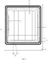
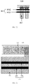
- FIG. 1 is a schematic structural diagram of a display substrate according to an embodiment of the present disclosure.
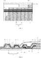
- FIG. 2 is a sectional view of the display substrate shown in FIG. 1 taken along a direction of BB.
- the display substrate may be a flexible panel, and may be, for example, a foldable panel.
- the display substrate may include: a base substrate 001, a plurality of pixel units 002, at least one first power line 003, a blocking structure 004, an auxiliary connection structure 005, a cathode layer 006 and a first organic pattern 007.
- the plurality of pixel units 002 may be located on the base substrate 001.
- the auxiliary connection structure 005 the cathode layer 006 is not shown in FIG. 1 .
- the at least one first power line 003 is located on the base substrate 001.
- the blocking structure 004 may surround the plurality of pixel units 002.
- the auxiliary connection structure 005 may include a first side surface 005a and a second side surface 005b which are opposite to each other, and the first side surface 005a is closer to the plurality of pixel units 002 than the second side surface 005b is.
- the cathode layer 006 may be located on a side of the auxiliary connection structure 005 distal from the base substrate 001.
- the first organic pattern 007 may be located on the side of the auxiliary connection structure 005 distal from the base substrate 001.
- One end 003a of the at least one first power line 003 is located on a side of the blocking structure (the dam structure) 004 distal from the plurality of pixel units 002 and is configured for receiving a power signal.
- the other end 003b of the at least one first power line 003 is located between the blocking structure 004 and the plurality of pixel units 002 and is connected with the cathode layer 006 through the auxiliary connection structure 005, thereby enabling the first power line 003 to provide the power signal to the cathode layer 006.
- each first power line 003 is located outside a region surrounded by the blocking structure (the dam structure) 004, and the other end is located within the region surrounded by the blocking structure 004, i.e., each first power line 003 can pass through the blocking structure 004 to enter the region surrounded by the blocking structure 004.
- the portion of the blocking structure 004 configured for allowing the power line to pass through can also be referred to as a line inlet port.
- the portion allowing the first power line 003 to pass through may be referred to as a first line inlet port 00a.
- first power lines 003 are illustrated in FIG. 1 , and the end 003a of each first power line 003 is connected with a driving chip for receiving the power signal provided by the driving chip.
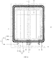
- FIG. 3 is a schematic structural diagram of another display substrate according to an embodiment of the present disclosure.
- FIG. 4 is a local schematic structural diagram of a display substrate according to an embodiment of the present disclosure.
- an orthographic projection of the auxiliary connection structure 005 on the base substrate 001 may include a first projection region 005c and a second projection region 005d.
- the first projection region 005c is closer to the end 003a of the at least one first power line 003 for receiving the power signal than the second projection region 005d is.
- the first projection region 005c and an orthographic projection of the blocking structure 004 on the base substrate 001 do not overlap; and the second projection region 005d and the orthographic projection of the blocking structure 004 on the base substrate 001 overlap to form a region including a first overlapping region 00b.
- the first power line 003, a second power line 008 and the cathode layer 006 are not shown in FIG. 3 .
- a first organic pattern 005 may be generally configured to cover at least a part of the second side surface 005b, thereby guaranteeing that the auxiliary connection structure 005 can effectively transmit the power signal from the first power line 003.
- the organic material for manufacturing the first organic pattern 007 is a hydrophilic material, therefore, by disposing the first projection region 005c formed from the orthographic projection of the auxiliary connection structure 005 on the base substrate 001 as not overlapping with the orthographic projection of the blocking structure 004 on the base substrate 001, the first organic pattern 007 is configured to be not in contact with the blocking structure 004 when it covers at least a part of the second side surface 005a of the auxiliary connection structure 005 at the first projection region 005c, i.e., the first organic pattern 007 is configured to be spaced apart from the blocking structure 004; and therefore, the moisture brought in by the end 003a of the first power line 003 for receiving the power signal can be prevented from being further introduced into the plurality of pixel units 002 through the blocking structure 004 and the first organic pattern 007, thereby guaranteeing the yield of the display substrate.
- the width of a lap joint between the auxiliary connection structure 005 and the first power line 003 can be relatively wide, so as to guarantee that the contact resistance between the auxiliary connection structure 005 and the first power line 003 is as small as possible.
- an orthographic projection of the lap joint on the base substrate is an area where the first projection region 005c and the orthographic projection of the first power line 003 on the base substrate 001 overlap.
- the width of other portions of the auxiliary connection structure 005 distal from the lap joint may be narrow, so as to reduce the capacitive coupling effect on other signal lines provided on the side of the auxiliary connection structure 005 proximal to the base substrate. For example, the capacitive coupling effect on the data lines can be reduced.
- the embodiments of the present disclosure provide a display substrate, which includes a base substrate, a plurality of pixel units, at least one first power line, a blocking structure, an auxiliary connection structure, a cathode layer and a first organic pattern.
- a first projection region of an orthographic projection of the auxiliary connection structure on the base substrate and an orthographic projection of the blocking structure on the base substrate do not overlap, such that the first organic pattern is spaced apart from the blocking structure; and therefore, the moisture brought in by one end of the first power line for receiving a power signal can be prevented from being introduced into the pixel units through the blocking structure and the first organic pattern, thereby guaranteeing the yield of the display substrate, as well as the display effect of the display substrate.
- the region where the orthographic projections of the plurality of pixel units 002 on the base substrate 001 are located may be an active area (AA) of the display substrate, also known as a display region or an AA region. Therefore, the blocking structure 004 can be disposed to surround the AA region.
- the cathode layer 006 may form an entire layer to cover the AA region.
- the orthographic projection of the cathode layer 006 on the base substrate 001 may cover the orthographic projections of the plurality of pixel units 002 on the base substrate 001; and the orthographic projection of the cathode layer 006 on the base substrate 001 may be inside the orthographic projection of the region surrounded by the blocking structure 004 on the base substrate 001.
- the first organic pattern 007 may cover at least a portion of the second side surface 005b of the auxiliary connection structure 005; an orthographic projection of the first organic pattern 007 and the orthographic projection of the at least one first power line 003 on the base substrate 001 overlap at a second overlapping region 00c, and the second overlapping region 00c and the orthographic projection of the blocking structure 004 on the base substrate 001 do not overlap.
- the risk of the second side surface of the auxiliary connection structure 005 being eroded by moisture or oxygen due to the etching defect can be reduced, thereby guaranteeing that the auxiliary connection structure 005 can effectively transmit the power signal from the first power line 003.
- the organic material for manufacturing the first organic pattern 007 is typically a hydrophilic material, therefore, by disposing the second overlapping region 00c as not overlapping with the orthographic projection of the blocking structure 004 on the base substrate, i.e., making the first organic pattern 007 be spaced apart from the blocking structure 004, the moisture brought in by the end 003a of the first power line 003 for receiving the power signal can be prevented from being introduced into the pixel unit 002 through the blocking structure 004 and the first organic pattern 007, thereby guaranteeing the yield of the display substrate.
- a distance between the second overlapping region 00c, where the orthographic projection of the first organic pattern 007 and the orthographic projection of the at least one first power line 003 on the base substrate 001 overlap, and the orthographic projection of the blocking structure 004 on the base substrate 001 may be greater than a threshold distance.
- the threshold distance may be in a range from 80 microns( ⁇ m) to 150 ⁇ m.
- the threshold distance may be 90 ⁇ m, 100 ⁇ m, 110 ⁇ m, 120 ⁇ m, 130 ⁇ m, 140 ⁇ m, etc. That is, a certain distance is presented between the first organic pattern 007 and the blocking structure 004.
- the first organic pattern 007 can be prevented from directly contacting the blocking structure 004 near the first line inlet port 00a of the first power line 003, and the moisture can be further prevented from being introduced into the pixel unit 002 through the first organic pattern 007, thereby guaranteeing the encapsulation effect.
- the threshold distance may be a threshold that is determined in advance through experiments as being able to prevent the moisture from entering the pixel units 002. That is, when the distance between the second overlapping region 00c and the blocking structure 004 is greater than the threshold distance, it is hard for the moisture to enter the pixel units 002 in the display substrate.
- the threshold distance may be a threshold that is determined in advance through experiments as being able to prevent the moisture from entering the pixel units 002. That is, when the distance between the second overlapping region 00c and the blocking structure 004 is greater than the threshold distance, the moisture would not enter the pixel units 002 in the display substrate.
- the second side surface 005b of the auxiliary connection structure 005 may also be covered by the blocking structure 004. That is, the second side surface 005b of the auxiliary connection structure 005 in the second projection region 005d may be covered by the blocking structure 004.
- the area of the base substrate 001 occupied by the auxiliary connection structure 005 and the blocking structure 004 can be reduced, facilitating the realization of a narrow-frame display substrate.
- the second projection region 005d of the auxiliary connection structure 005 has a longer distance from the first portion 0081 of the at least one second power line 008. Referring to FIG. 6 , at a position distal from a second line inlet port 00d, a long entrance path is formed for the moisture, even if the second side surface 005b of the auxiliary connection structure 005 is covered by the blocking structure 004, the moisture cannot enter the pixel units 002.
- the auxiliary connection structure 005 may be in a ring construction surrounding the plurality of pixel units 002, so as to facilitate the cathode layer 006 to be connected to the at least one first power line 003 through the auxiliary connection structure 005, thereby guaranteeing the uniformity of potential of the power signal provided to the pixel units 002 of the display substrate, and achieving a good display effect.
- the end 003a of the at least one first power line 003 may be located in a middle of the side of the blocking structure 004 distal from the plurality of pixel units 002, for example, in the middle of the bonding region 00e.
- the middle is a position where the longitudinal axis X of the base substrate passes through, and the longitudinal axis X is an axis parallel to the data line on the base substrate 001.
- a distance between the longitudinal axis X and one side of the display substrate is approximately equal to a distance between the longitudinal axis X and the other side of the display substrate.
- the one side and the other side are approximately parallel to an extension direction of the data line. For example, an included angle between any one of the two sides of the display substrate approximately parallel to the extension direction of the data line and the extension direction of the data line ranges from 0 degree to 10 degrees.
- “approximately” in the embodiments of the present disclosure refers to that an error range within 15% is allowed. If the distances are “approximately” equal to each other, then a difference between the two distances is no more than 15%. If the extension directions are “approximately” parallel to each other, then the included angle of the two extension directions is between 0 degree and 30 degrees, such as 0 degree to 10 degrees, 0 degree to 15 degrees and so on. If the shapes are “approximately” the same with each other, then the two shapes are of the same type, such as a rectangle, a polyline, an arc, a strip, an "L” type and so on. If the areas are “approximately” the same, then a difference between the two areas does not exceed 15%, etc.
- the display substrate may include two first power lines 003.
- the two first power lines 003 may be adjacently arranged in the middle of the side of the blocking structure 004 distal from the plurality of pixel units 002.
- the two first power lines 003 are arranged in the middle of the side of the blocking structure 004 away from the plurality of pixel units 002, and are spaced from each other to be symmetrical with each other with respect to the longitudinal axis X of the base substrate as a symmetric axis.
- the arranging positions of the first power lines 003 are not limited in the embodiment of the present disclosure.
- the two first power lines 003 When the two first power lines 003 are adjacently arranged in the middle of the side of the blocking structure 004 distal from the plurality of pixel units 002, the two first power lines 003 may be formed to be a structure formed integrally.
- the two first power lines 003 are formed integrally, that is, when there is one first power line 003, one end 003a of the first power line 003 is located in the middle of the side of the blocking structure 004 distal from the plurality of pixel units 002, for example, located in the middle of the bonding region 00e, so that the distance from the end 003a of the first power line 003 to the longitudinal axis X is less than the distance from the end 003a of the first power line 003 to any side of the two sides approximately parallel to the longitudinal axis X of the display substrate.
- a folding line of the foldable panel may be perpendicular to the longitudinal axis X.
- the folding line of the foldable panel may be a perpendicular bisector of the longitudinal axis X.
- the display substrate may further include: at least one second power line 008.
- the at least one second power line 008 may include a first portion 0081 and a second portion 0082.
- the first portion 0081 may be located on the side of the blocking structure 004 distal from the plurality of pixel units 002, and is configured for receiving a power signal.
- the first portion 0081 may be connected with a driving chip and configured for receiving a power signal provided by the driving chip.
- the second portion 0082 may be connected with the cathode layer 006 through the auxiliary connection structure 005.
- FIG. 5 is a local schematic structural diagram of the display substrate shown in FIG. 1 .
- the second portion 0082 may include a first junction 0082a and a second junction 0082b which are both connected with the auxiliary connection structure 004, and a distance between the first junction 0082a and the blocking structure 004 may be greater than a distance between the second junction 0082b and the blocking structure 005. That is, the first junction 0082a of the second portion 0082 of the at least one second power line 008 is not in contact with the blocking structure 004.
- an orthographic projection of the first junction 0082a on the base substrate 001 and an orthographic projection of the blocking structure 004 on the base substrate 001 do not overlap; and the second junction 0082b may be located within a region covered by the blocking structure 004, for example, the second junction 0082b may be in contact with the blocking structure 004.
- the display substrate may further have a bonding region 00e, which may be located on the side of the blocking structure distal from the plurality of pixel units 002.
- the first junction 0082a is closer to the bonding region 00e than the second junction 0082b is.
- “being closer” means that the shortest distance between the respective points of the first junction 0082a and the bonding region 00e is greater than the shortest distance between the respective points of the second junction 0082b and the bonding region 00e.
- each junction of the first junction 0082a and the second junction 0082b may refer to: a portion of the second portion 0082 of the second power line 008 which is in contact with the auxiliary connection structure 005.
- the junction may refer to a portion of the second portion 0082 which is in direct contact with the auxiliary connection structure 005.
- the shapes of the two junctions may be substantially the same as the shape of the region where the orthographic projection of the second portion 0082 on the base substrate 001 and the orthographic projection of the auxiliary connection structure 005 on the base substrate 001 overlap.
- the second power line 008 may include two first portions 0081.
- the two first portions 0081 may be substantially symmetrically disposed, with respect to the longitudinal axis X of the base substrate 001, around an edge of a side of the blocking structure 004 distal from the plurality of pixel units 002.
- the second power line 008 may include two first portions 0081.
- the two first portions 0081 may be located on two sides of the longitudinal axis X respectively, such as at two sides of the bonding region 00e.
- the second power line 008 may include two first portions 0081.
- the part of the two first portions 0081 which are near the second line inlet port 00d are respectively located at two sides of the display substrate, in another example, respectively proximal to two side edges that are parallel to the longitudinal axis X.
- the second line inlet port 00d may be a portion of the blocking structure 004 for allowing the second power line 008 to pass through.
- both the first power line 003 in the middle and the second power line 008 at the edge provide the power signal to the cathode layer 006 in the display substrate at the same time, so as to further alleviate the problem that a potential difference of the power signal loaded to the cathode layers 006 in different regions is large due to voltage drop.
- the cathode layer 006 has good long range uniformity (LRU) and an improved display effect.
- both the first power line 003 in the middle and the second power line 008 at the edge provide the power signal to the cathode layer 006 in the display substrate.
- the design of the first power line 003 in the embodiments of the present disclosure can favorably mitigate the moisture and oxygen erosions and guarantee a good encapsulation performance.
- more first power lines 003 may be provided.
- the uniformity of potential in respective regions of the cathode layer 006 can be guaranteed and the display substrate can achieve an improved display effect.
- both the first power line 003 and the second power line 008 are configured to provide the power signal to the cathode layer 006, both the first power line 003 and the second power line 008 may be referred to as a VSS power line or a VSS wire.
- the display substrate may further include: a row driving region 00f located between the blocking structure 004 and the plurality of pixel units 002.
- a distance between the row driving region 00f and the orthographic projection of the at least one first power line 003 on the base substrate 001 may be greater than a distance between the row driving region 00f and the orthographic projection of the at least one second power line 008 on the base substrate.
- the distance between the at least one first power line 003 located in the middle and the row driving region 00f may be longer than the distance between the at least one second power line 008 and the row driving region 00f.
- the shortest distance between respective portions of each first power line 003 and the row driving region 00f is greater than the shortest distance between respective portions of each second power line 008 and the row driving region 00f.
- the distance h1 between a point a1 of the at least one first power line 003 and the row driving region 00f is greater than the distance h2 between a point b1 of the at least one second power line 008 and the row driving region 00f.
- the row driving region 00f may be provided with a plurality of cascaded shift register units, which may be configured to drive each row of the pixel units 002.
- the display substrate may have two row driving regions 00f, which are respectively arranged on two sides of the plurality of pixel units 002 and are symmetrically arranged with the longitudinal axis X of the base substrate 001 as the symmetrical axis.
- the display substrate may further include: a passivation layer 009 which may cover the at least one first power line 003.
- FIG. 7 is a local schematic structural diagram of another display substrate according to an embodiment of the present disclosure. Referring to FIGS. 2 and 7 , the passivation layer 009 is further provided with an opening 009a; a side of the auxiliary connection structure 005 proximal to the base substrate 001 is connected with the at least one first power line 003 through the opening 009a, and a side of the auxiliary connection structure 005 distal from the base substrate 001 is connected with the cathode layer 006.
- the reference 009a shown in FIG. 7 is an opening provided in the passivation layer 009. That is, in FIG. 7 , except the region where the opening 009a is located, all other regions are covered by the passivation layer 009.
- the at least one first power line 003 is easy to be eroded by moisture or oxygen during the manufacturing of the display substrate, by covering the at least one first power line 003 with the passivation layer 009, it can be guaranteed that when other layers are formed subsequently, the at least one first power line 003 would not be eroded by moisture or oxygen, thereby guaranteeing that the at least one first power line 003 can provide the power signal to the cathode layer 006, so as to ensure the display effect of the display substrate.
- the opening in the passivation layer 009 may be a via hole or may be a slot, which is not limited in the embodiments of the present disclosure.
- the material for manufacturing the passivation layer 009 may include: one or more of inorganic oxides such as SiNx (silicon nitride), SiOx (silicon oxide) and SiOxNy (silicon oxynitride). The material for manufacturing the passivation layer 009 is not limited by the embodiments of the present disclosure.
- the passivation layer 009 may further cover the at least one second power line 008, thereby guaranteeing that the at least one second power line 008 would not be eroded by moisture or oxygen, so as to ensure the display effect of the display substrate.
- the blocking structure 004 may in a ring construction surrounding the plurality of pixel units 002 to block the overflow of an organic layer in the region surrounded by the blocking structure 004 of the display substrate.
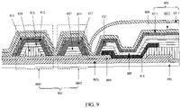
- the blocking structure 004 may include: a first blocking dam 0041 and a second blocking dam 0042.
- the first blocking dam 0041 is farther away from the plurality of pixel units 002 than the second blocking dam 0042 is, and the thickness of the first blocking dam 0041 is greater than the thickness of the second blocking dam 0042.
- the blocking structure 004 may further include one blocking dam, or more than two blocking dams, which is not limited in the embodiments of the present disclosure.
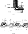
- FIG. 8 is a schematic structural diagram of still another display substrate according to an embodiment of the present disclosure.
- the first blocking dam 0041 may include: a first planarization layer pattern 010, a second planarization layerpattern 011 and a second organic pattern 012 which are disposed along a direction away from the base substrate 001.
- the second blocking dam 0042 may include: a third planarization layer pattern 013 and a third organic pattern 014 which are arranged along a direction away from the base substrate 001.
- the second planarization layer pattern 011 and the third planarization layer pattern 013 may include a same material; and the first organic pattern 007, the second organic pattern 012 and the third organic pattern 014 may include a same material.
- the second planarization layer pattern 011 and the third planarization layer pattern 013 may employ the same material and may be prepared from a same patterning process; and the first organic pattern 007, the second organic pattern 012 and the third organic pattern 014 may employ the same material and may be prepared from a same patterning process.
- the first planarization layer pattern 010 may belong to the first planarization layer; the second planarization layer pattern 011 and the third planarization layer pattern 013 may belong to the second planarization layer; and the first organic pattern 007, the second organic pattern 012 and the third organic pattern 014 may belong to the first organic layer which may be a pixel definition layer (PDL).
- PDL pixel definition layer
- the materials for manufacturing the first planarization layer, the second planarization layer and the first organic layer may include: organic materials such as resins. This is not limited in the embodiments of the present disclosure.
- the first blocking dam 0041 may include: a planarization layer pattern 015 and a second organic pattern 012 which are sequentially arranged in layers along a direction away from the base substrate 001.
- the second blocking dam 0042 may include: a third organic pattern 014 disposed on the base substrate 001.
- the first organic pattern 007, the second organic pattern 012 and the third organic pattern 014 may include a same material.
- the first organic pattern 007, the second organic pattern 012 and the third organic pattern 014 may employ the same material and may be prepared from a same patterning process.
- the planarization layer pattern 015 may belong to the planarization layer; and the first organic pattern 007, the second organic pattern 012 and the third organic pattern 014 may belong to the first organic layer.
- the materials for manufacturing the planarization layer may include: organic materials such as resins. This is not limited in the embodiments of the present disclosure.
- the opening 015a shown in FIG. 7 is a region not covered by the planarization layer pattern 015.
- the planarization layer pattern 015 may cover a boundary of a portion of the first power line 003 located in the region surrounded by the blocking structure 004.
- the region where the overlapping region and the orthographic projection of the opening 009a of the planarization layer 009 on the base substrate 001 overlap may cover the region where the overlapping region and the orthographic projection of the opening 015a of the planarization layer pattern 015 on the base substrate 001 overlap. That is, in the overlapping region, the size of the opening 009a of the planarization layer 009 is greater than the size of the opening 015a of the planarization layer pattern 015.
- the first blocking dam 0041 has one more planarization layer pattern than the second blocking dam 0042, so that the thickness of the first blocking dam 0041 is greater than the thickness of the second blocking dam 0042, which prevents the overflow of the organic layer.
- FIG. 9 is a schematic structural diagram of still another display substrate according to an embodiment of the present disclosure.
- the first blocking dam 0041 may further include: a fourth organic pattern 016 disposed on a side of the second organic pattern 012 distal from the base substrate 001.
- the second blocking dam 0042 may further include: a fifth organic pattern 017 disposed on a side of the third organic pattern 014 distal from the base substrate 001.
- the fourth organic pattern 016 and the fifth organic pattern 017 may include a same material.
- the fourth organic pattern 016 and the fifth organic pattern 017 may employ the same material and may be prepared from a same patterning process.
- both the fourth organic pattern 016 and the fifth organic pattern 017 may belong to the second organic layer, which may be a photo spacer (PS).
- PS photo spacer
- the materials for manufacturing the second organic layer may include: organic materials such as resins. This is not limited in the embodiments of the present disclosure.
- FIG. 10 is a schematic structural diagram of still another display substrate according to an embodiment of the present disclosure.
- the first organic pattern 007 may cover the second side surface 005b of the auxiliary connection structure 005.
- the first blocking dam 0041 may be a first ring
- the second blocking dam 0042 may be a second ring.
- the first organic pattern 007 and a portion of the third organic pattern 014 may define a third ring.
- An orthographic projection of the third ring on the base substrate 001 may be located inside an orthographic projection of the second ring on the base substrate 001, and the orthographic projection of the second ring on the base substrate 001 may be located inside an orthographic projection of the first ring on the base substrate 001.
- the third ring may surround the plurality of pixel units 002.
- the shape of the third organic pattern 014 may be substantially the same as that of the second blocking dam 0042, that is, the third organic pattern 014 may also be ring-shaped.
- the portion of the third organic pattern 014 may be a portion of the third organic pattern 014 located on the side of the first organic pattern 007 proximal to the plurality of pixel units 002.
- the portion of the third organic pattern 014 may be the left portion, the upper portion, and the right portion of the third organic pattern 014.
- the first organic pattern 007 may include a portion which is in direct contact with the second blocking dam 0042.
- the second power line 008 may include two first portions 0081 and one second portion 0082.
- the two first portions 0081 may be symmetrically disposed on two sides of the base substrate 001 with respect to the longitudinal axis X of the base substrate 001.
- the part of the two first portions 0081 near the second line inlet port 00d may be located on two sides of the display substrate, and in another example, may be respectively located close to each of the two side edges that are parallel to the longitudinal axis X.
- FIG. 6 shows the second line inlet port 00d of the two first portions 0081.
- the second portion 0082 may surround the plurality of pixel units 002, and the two ends of the second portion 0082 may be connected with one first portion 0081 respectively.
- first portion 0081 and the second portion 0082 may be in direct contact, for example, may be formed integrally.
- the second power line 008 may include: a straight portion 0082c and an arc-shaped portion 0082d which surround a region where the plurality of pixel units 002 are located.
- the second portion 0082 may include: a straight portion 0082c and an arc-shaped portion 0082d which surround a region where the plurality of pixel units 002 are located. Furthermore, the second portion 0082 of the second power line 008 may include a non-enclosed structure. The embodiments of the present disclosure take the second portion 0082 at least surrounding two edges of the display substrate as an example for description. An orthographic projection of a portion, in direct contact with the second blocking dam 0042, of the first organic pattern 007 on the base substrate 001 may be located within an orthographic projection of the arc-shaped portion 0082d on the base substrate 001.
- the orthographic projection of the portion, which is in direct contact with the second blocking dam 0042, of the first organic pattern 007 on the base substrate 001 does not go outside of the orthographic projection of the arc-shaped portion 0082d on the base substrate 001.
- the arc-shaped portion 0082d is closer to the first portion 0081 of the at least one second power line 008 for receiving the power signal than the straight portion 0082c is.
- the at least one first power line 003 may include: a first metal layer 003c.
- the display substrate may further include: an auxiliary metal layer 018 on a side of the first metal layer 003c distal from the base substrate 001.
- a side of the auxiliary metal layer 018 distal from the first metal layer 003c may be in contact with the auxiliary connection structure 005, and an orthographic projection of the auxiliary metal layer 018 on the base substrate 001 and the orthographic projection of the blocking structure 004 on the base substrate 001 do not overlap.
- the orthographic projection of the auxiliary metal layer 018 on the base substrate 001 includes a portion which is within a region surrounded by the orthographic projection of the blocking structure 004 on the base substrate 001.
- FIG. 12 is a local schematic structural diagram of still another display substrate according to an embodiment of the present disclosure.
- the orthographic projection of the auxiliary metal layer 018 on the base substrate 001 includes a portion which is within a region surrounded by the orthographic projection of the second blocking structure 0042 on the base substrate 001.
- the side of the first metal layer 003c distal from the base substrate 001 is not provided with the auxiliary metal layer 018 in the region where the blocking structure 004 is located. That is, in the region where the blocking structure 004 is located, the auxiliary metal layer 018 is removed. That is, in the region where the first line inlet port 00a is located, the auxiliary metal layer 018 is removed.
- the side of the blocking structure 004 distal from the plurality of pixel units 002 may be provided with an auxiliary metal layer 018; and the region surrounded by the blocking structure 004 may also be provided with an auxiliary metal layer 018.
- the shape of a boundary of the auxiliary metal layer 018 may be substantially the same as the shape of a boundary of the first metal layer 003c, or the shape of the boundary of the auxiliary metal layer 018 may also be different from the shape of the boundary of the first metal layer 003c. This is not limited in the embodiments of the present disclosure.
- the power signal received by the first metal layer 003c may be transmitted to the auxiliary connection structure 005 through the auxiliary metal layer 018 disposed in the opening of the passivation layer 009.
- the power signal is transmitted to the cathode layer 006 through the auxiliary connection structure 005.
- the side of the auxiliary metal layer 018 distal from the base substrate 001 may be covered, at portions close to the edges and at the side edges, by a second planarization layer including the second planarization layer pattern 011 and the third planarization layer pattern 013; and the second planarization layer can be configured to avoid display defects caused by etching defects on the sidewalls of the auxiliary metal layer 018.
- the organic material for manufacturing the second planarization layer is typically a hydrophilic material, therefore, in order to prevent the auxiliary metal layer 018 from introducing moisture into the pixel units 002, the orthographic projection of the auxiliary metal layer 018 on the base substrate 001 and the orthographic projection of the blocking structure 004 on the base substrate 001 can be configured to have no overlapped region, such that the moisture can be prevented from entering inside from the blocking structure 004 and entering the region where the pixel units 002 are located along the path formed by the second planarization layer, thereby guaranteeing the display effect of the display substrate.
- FIG. 13 is a local schematic structural diagram of still another display substrate according to an embodiment of the present disclosure.
- the orthographic projection of a portion of the auxiliary metal layer 018 in contact with the first metal layer 003c, on the base substrate 001 may be located within the orthographic projection of the auxiliary metal layer 018 on the base substrate 001, so that a distance is presented between the boundary of the first metal layer 003c and the boundary of the auxiliary metal layer 018.
- the first metal layer 003c and the auxiliary metal layer 018 can be prevented from being eroded by the moisture or oxygen.
- FIG. 14 is a local schematic structural diagram of still another display substrate according to an embodiment of the present disclosure. The reference 010a shown in FIG.
- FIG. 14 illustrates an opening provided in the first planarization layer. That is, in FIG. 14 , except the region where the opening 010a is located, all other regions are covered with the first planarization layer.
- the reference 011a shown in FIG. 14 illustrates an opening provided in the second planarization layer. That is, in FIG. 14 , except the region where the opening 011a is located, all other regions are covered with the second planarization layer.
- the first metal layer 003c, the passivation layer 009, the first planarization layer pattern 010, the auxiliary metal layer 018, the second planarization layer pattern 011 and the first organic pattern 007 of the display substrate may be arranged in layers along a direction away from the base substrate 001. That is, the first power line 003, the passivation layer 009, the first planarization layer, the auxiliary metal layer 018, the second planarization layer and the first organic layer of the display substrate may be arranged in layers along the direction of the base substrate 001.
- both the first metal layer 003c and the auxiliary metal layer 018 may include three metal film layers.
- the materials of the three metal film layers may sequentially be: titanium (Ti), aluminum (Al) and Ti.
- FIG. 15 is a sectional view of the display substrate shown in FIG. 1 taken along a direction of CC.
- the at least one second power line 008 may include: a second metal layer 008a.
- the display substrate may further include: an auxiliary wiring layer 019 on a side of the second metal layer 008a distal from the base substrate 001.
- a side of the auxiliary wiring layer 019 distal from the second power line 008 is in contact with the auxiliary connection structure 005, and an orthographic projection of the auxiliary wiring layer 019 on the base substrate 001 and the orthographic projection of the blocking structure 004 on the base substrate 001 does not overlap.
- the orthographic projection of the auxiliary wiring layer 019 on the base substrate 001 may include a portion which is within the orthographic projection of the blocking structure 004 on the base substrate 001.
- FIG. 16 is a local schematic structural diagram of still another display substrate according to an embodiment of the present disclosure.
- the orthographic projection of the auxiliary wiring layer 019 on the base substrate 001 may have a portion which is within the orthographic projection of the second blocking structure 0042 on the base substrate 001.
- the side of the second metal layer 008a distal from the base substrate 001 is not provided with the auxiliary wiring layer 019 in the region where the blocking structure 004 is located. That is, in the region where the blocking structure 004 is located, the auxiliary wiring layer 01 is removed. That is, in the region where the second line inlet port 00d is located, the auxiliary wiring layer 019 is removed.
- the side of the blocking structure 004 distal from the plurality of pixel units may be provided with the auxiliary wiring layer 019; and the region included in the blocking structure 004 may be provided with the auxiliary wiring layer 019.
- the shape of a boundary of the auxiliary wiring layer 019 may be substantially the same as the shape of a boundary of the second metal layer 008a, or the shape of the boundary of the auxiliary wiring layer 019 may be different from the shape of the boundary of the second metal layer 008a. This is not limited in the embodiments of the present disclosure.
- the at least one first power line 003 may include: a first metal layer 003c and a third metal layer 003d which are disposed along a direction away from the base substrate 001. A side of the third metal layer 003d distal from the first metal layer 003c is in contact with the auxiliary connection structure 005.
- Both the orthographic projection of the first metal layer 003c on the base substrate 001 and the orthographic projection of the third metal layer 003d on the base substrate 001 may overlap with the orthographic projection of the blocking structure 004 on the base substrate 001. That is, the ends of both the first metal layer 003c and the third metal layer 003d distal from the plurality of pixel units 002 can be configured to receive the power signal, so that the power signal can be transmitted to the cathode layer 006 through both the first metal layer 003c and the third metal layer 003d. Therefore, the resistance can be reduced and the voltage drop of the power signal can be further reduced.
- the orthographic projection of the first metal layer 003c on the base substrate 001 and the region where the third metal layer 003d is in contact with the auxiliary connection structure 005 do not overlap.
- the orthographic projection of the first metal layer 003c on the base substrate 001 may overlap with the region where the third metal layer 003d is in contact with the auxiliary connection structure 005.
- the first planarization layer may cover the other end of the first metal layer 003c proximal to the plurality of pixel units 002, so as to reduce the oxygen or moisture corrosions occurring on the other end of the first metal layer 003c, or to reduce the final display defects caused by the etching defects of the side surfaces of the metal layers.
- the first metal layer 003c, the first planarization layer pattern 010, the third metal layer 003d, the passivation layer 009, the second planarization layer pattern 011 and the first organic pattern 007 of the display substrate may be arranged in layers along a direction away from the base substrate 001. That is, the first metal layer pattern 003a, the first planarization layer, the third metal layer 003d, the passivation layer 009, the second planarization layer, and the first organic layer of the display substrate may be arranged in layers along the direction of the base substrate 001.
- both the first metal layer 003c and the third metal layer 003d may include three metal film layers.
- the materials of the three metal film layers may sequentially be: Ti, Al and Ti.
- the first blocking dam 0041 further includes a fourth organic pattern 016 disposed on a side of the second organic pattern 012 distal from the base substrate
- the second blocking dam 0042 further includes a fifth organic pattern 017 disposed on a side of the third organic pattern 014 distal from the base substrate 001
- the second organic layer including the fourth organic pattern 016 and the fifth organic pattern 017 can be disposed on a side of the first organic layer distal from the base substrate 001.
- FIG. 19 is a schematic structural diagram of still another display substrate according to an embodiment of the present disclosure.
- a plurality of tooth-shaped protruding structures are formed on a side surface of the at least one first power line 003 located on the side of the blocking structure 004 distal from the plurality of pixel units 002. Therefore, an entrance path of moisture can be further prolonged, and the moisture can be prevented from being introduced into the plurality of pixel units 002.
- orthographic projections of the protruding structures on the base substrate 001 and the orthographic projection of the blocking structure 004 on the base substrate 001 do not overlap.
- a side surface of the other end 003b of the at least one first power line 003 within the region surrounded by the blocking structure 004 may be flat. That is, no protruding structure is formed on the side surface of the other end 003b of the at least one first power line 003 within the region surrounded by the blocking structure 004.
- the auxiliary connection structure 005 is obtained by sequential processes such as exposure, development, etching and other processes. In the etching process, an etchant is needed for etching a film layer. If the side surface of the other end 003b of the first power line 003 within the region surrounded by the blocking structure 004 is also configured to have tooth-shaped protruding structures, the etchant will be retained among the adjacent protruding structures of the first power line 003, so that the sidewall of the other end 003b of the first power line 003 will be corroded.
- the passivation layer 009 which is a brittle film on the side of the first power line 003 distal from the base substrate 001 can be prevented from being penetrated through, due to the corrosion on the sidewall of the first power line 003, in the process of manufacturing the display substrate.
- the quality of the passivation layer 009 can be guaranteed.
- a plurality of tooth-shaped protruding structures may also be formed on a side surface of an end, distal from the plurality of pixel units 002, of a first portion 0081 of the at least one second power line 008. Therefore, an entrance path of moisture along the second power line 008 can be prolonged, and the moisture can be prevented from being introduced into the plurality of pixel units 002. Furthermore, the side surface of the other end, within the region surrounded by the blocking structure 004, of the first portion 0081 of the at least one second power line 008 may be flat.
- the display substrate may further include: a plurality of third power lines 020, which may be located on the base substrate 001.
- the plurality of third power lines 020 are electrically connected with transistors in the pixel units 002 of the display substrate.
- the third power lines 020 may be respectively connected with a source electrode or a drain electrode of the transistors in the pixel units 002.
- the third power line 020 may be configured to provide a positive power signal to the transistor in the pixel units 002, such that the third power lines 020 may also be referred to as VDD power lines or a VDD wires.
- the plurality of third power lines 020 may be symmetrically disposed on two sides of the at least one first power line 003.
- the display substrate may include: four third power lines 020.
- two of the third power lines 020 may be located in the middle of the side of the blocking structure 004 distal from the plurality of pixel units 002; and the two third power lines 020 may be symmetrically disposed on two sides of the first power line 003 with respect to the longitudinal axis X of the base substrate 001.
- the remaining two third power lines 020 may be both located at an edge of the side of the blocking structure distal from the plurality of pixel units 002.
- Each third power line 020 may be located on the side of one first portion 0081 of the second power line 008 proximal to the first power line 003.
- a plurality of tooth-shaped protruding structures may also be formed on side surfaces of the ends of the plurality of third power lines 020 that are located on the side of the blocking structure 004 distal from the plurality of pixel units 002, so that the paths of introducing moisture along the third power lines 020 are extended to avoid moisture from being introduced into the plurality of pixel units 002.
- the side surface of the other end of each of the third power lines 0200 that is within the region surrounded by the blocking structure 004 may be flat.
- the display substrate may further include: an encapsulation film layer 021.
- the encapsulation film layer 021 may be located on a side of the plurality of first power lines distal from the base substrate 001, and the encapsulation film layer 021 may cover the region surrounded by the blocking structure 004.
- the encapsulation film layer 021 may include: a first film layer 0211, a second film layer 0212 and a third film layer 0213 disposed in layers in a direction away from the base substrate 001.
- the first film layer 0211 and the third film layer 0213 may be made of inorganic materials, and the second film layer 0212 may be made of an organic material.
- the first film layer 0211 and the third film layer 0213 may be made of one or more inorganic oxides such as SiNx, SiOx and SiOxNy.
- the second film layer 0212 may be made of a resin material.
- the resin material may be thermoplastic resin or a thermosetting resin.
- the thermoplastic resin may include acrylic (PMMA) resins, and the thermosetting resin may include epoxy resins.
- the second film layer 0212 may be located within the region surrounded by the blocking structure 004, and the first film layer 0211 and the third film layer 0213 may cover the region surrounded by the blocking structure 004 and further cover the blocking structure 004. That is, the orthographic projection of the blocking structure 004 on the base substrate 001 may be located within the region covered by the encapsulation film layer 021. As such, the encapsulation film layer 021 is ensured to effectively encapsulate respective structures located in the region surrounded by the blocking structure 004.
- the second film layer 0212 may be manufactured by an ink jet printing (IJP) method.
- the first film layer 0211 and the third film layer 0213 may be manufactured by a chemical vapor deposition (CVD) method.
- FIG. 20 is a schematic structural diagram of still another display substrate according to an embodiment of the present disclosure.
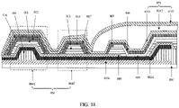
- a buffer layer 022, a semiconductor layer 023, a gate insulating layer 024, a gate electrode 025, an interlayer dielectric layer 026 and a source-drain electrode layer 027 may be sequentially disposed on the base substrate 001; and the source-drain electrode layer 027 may include a source electrode 0271 and a drain electrode 0272.
- the source electrode 0271 and the drain electrode 0272 are spaced apart from each other, and may be connected with the semiconductor layer 023 through via holes, respectively.
- a passivation layer 009, a first planarization layer 028, a second planarization layer 029 and a light-emitting element are sequentially disposed on the source-drain electrode layer 027 along a direction away from the base substrate 001.
- the light-emitting element may include an anode layer 030, a light-emitting layer 031 and a cathode layer 006 which are sequentially disposed in layers.
- the anode layer 030 may be electrically connected with the drain electrode 0272 through a via hole.
- the gate electrode 025, the source electrode 0271 and the drain electrode 0272 constitute a transistor, and each light-emitting element and the transistor to which the light-emitting element is connected may constitute a pixel unit 002.
- the first metal layer 003c included in the first power line 003 may be disposed on the same layer as the source-drain electrode layer 027.
- the auxiliary connection structure 005 may be disposed in a same layer as the anode layer 030 of the pixel.
- the auxiliary connection structure 005 may include three film layers.
- the materials of the three film layers may sequentially be: indium tin oxide (ITO), silver (Ag) and ITO.
- FIG. 21 is a schematic structural diagram of still another display substrate according to an embodiment of the present disclosure.
- the orthographic projections of the plurality of third power lines 020 on the base substrate 001 may have an overlapping region with the orthographic projection of the auxiliary connection structure 005 on the base substrate 001.
- the passivation layer 009 may be provided between the plurality of third power lines 020 and the auxiliary connection structure 005.
- the plurality of third power lines 020 are not in contact with the auxiliary connection structure 005.
- the embodiments of the present disclosure provide a display substrate, which includes a base substrate, a plurality of pixel units, at least one first power line, a blocking structure, an auxiliary connection structure, a cathode layer and a first organic pattern.
- a first projection region of an orthographic projection of the auxiliary connection structure on the base substrate and an orthographic projection of the blocking structure on the base substrate do not overlap, such that the first organic pattern is spaced apart from the blocking structure; and therefore, the moisture brought in by one end of the first power line for receiving a power signal can be prevented from being introduced into the pixel units through the blocking structure and the first organic pattern, thereby guaranteeing the yield of the display substrate, as well as the display effect of the display substrate.
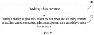
- FIG. 22 is a flowchart of a method for manufacturing a display substrate according to an embodiment of the present disclosure.
- the method may be used for manufacturing the display substrate according to the above embodiments.
- the method may include:
- One end 003a of the at least one first power line 003 may be located on a side of the blocking structure 004 distal from the plurality of pixel units 002 and is configured for receiving a power signal, and the other end 003b is located between the blocking structure 004 and the plurality of pixel units 002 and is connected with the cathode layer 006 through the auxiliary connection structure 005.
- the blocking structure 004 may surround the plurality of pixel units 002.
- the auxiliary connection structure 005 may include a first side surface 005a and a second side surface 005b opposite to each other.
- the first side surface 005a is closer to the plurality of pixel units 002 than the second side surface 005b is.
- An orthographic projection of the auxiliary connection structure 005 on the base substrate 001 has a first projection region 005c and a second projection region 005d.
- the first projection region 005c and an orthographic projection of the blocking structure 004 on the base substrate 001 do not overlap, and the second projection region 005d and the orthographic projection of the blocking structure 004 on the base substrate 001 overlap at a first overlapping regions 00b.
- the first projection region 005c is closer to the end 003a of the at least one first power line 003 for receiving the power signal than the second projection region 005d is.
- the at least one first power line 003 may be first formed on the base substrate 001, and then the blocking structure 004 and the auxiliary connection structure 005 may be formed on the side of the first power line 003 distal from the base substrate 001. Then, the first organic pattern 007 is formed on the side of the auxiliary connection structure 005 distal from the base substrate 001, and finally, the cathode layer 006 is formed on the side of the first organic pattern 007 distal from the base substrate 001.
- the at least one first power line 003 may be formed in a same patterning process as the source electrode and the drain electrode of the thin film transistor in the pixel unit 002.
- the blocking structure 004 may be formed in the process of forming the planarization layer, the pixel definition layer and the photo spacer.
- the first organic pattern 005 may be formed in the process of forming the pixel definition layer.
- the auxiliary connection structure 005 may be formed in a same patterning process as the anode layer 030 in the pixel unit 002.
- the embodiments of the present disclosure provide a method for manufacturing a display substrate.
- the method may include: sequentially forming a plurality of pixel units, at least one first power line, a blocking structure, an auxiliary connection structure, a first organic pattern and a cathode layer on the base substrate.
- a first projection region of an orthographic projection of the auxiliary connection structure on the base substrate and an orthographic projection of the blocking structure on the base substrate do not overlap, such that the first organic pattern is spaced apart from the blocking structure; and therefore, the moisture brought in by one end of the first power line for receiving a power signal can be prevented from being introduced into the pixel units through the blocking structure and the first organic pattern, thereby guaranteeing the yield of the display substrate, as well as the display effect of the display substrate.
- the embodiments of the present disclosure further provide a display apparatus, which may include any one of the display substrates described in the above embodiments.
- the display apparatus may be a display apparatus having a foldable screen, and for example, a liquid crystal panel, electronic paper, an organic light-emitting diode (OLED) panel, an active-matrix organic light-emitting diode (AMOLED) panel, a mobile phone, a tablet computer, a television, a display, a notebook computer, a digital photo frame or a navigator and other products or components with a display function.
- OLED organic light-emitting diode
- AMOLED active-matrix organic light-emitting diode
Landscapes
- Engineering & Computer Science (AREA)
- Microelectronics & Electronic Packaging (AREA)
- Physics & Mathematics (AREA)
- Optics & Photonics (AREA)
- Geometry (AREA)
- Electroluminescent Light Sources (AREA)
- Devices For Indicating Variable Information By Combining Individual Elements (AREA)
Applications Claiming Priority (1)
| Application Number | Priority Date | Filing Date | Title |
|---|---|---|---|
| PCT/CN2019/098939 WO2021017012A1 (zh) | 2019-08-01 | 2019-08-01 | 显示基板及显示装置 |
Publications (2)
| Publication Number | Publication Date |
|---|---|
| EP4009372A1 true EP4009372A1 (de) | 2022-06-08 |
| EP4009372A4 EP4009372A4 (de) | 2022-08-17 |
Family
ID=74228514
Family Applications (1)
| Application Number | Title | Priority Date | Filing Date |
|---|---|---|---|
| EP19933243.8A Pending EP4009372A4 (de) | 2019-08-01 | 2019-08-01 | Anzeigesubstrat und anzeigevorrichtung |
Country Status (4)
| Country | Link |
|---|---|
| US (1) | US20210225994A1 (de) |
| EP (1) | EP4009372A4 (de) |
| CN (1) | CN112602198A (de) |
| WO (1) | WO2021017012A1 (de) |
Families Citing this family (5)
| Publication number | Priority date | Publication date | Assignee | Title |
|---|---|---|---|---|
| US20210225992A1 (en) * | 2019-08-01 | 2021-07-22 | Boe Technology Group Co., Ltd. | Display substrate and display device |
| KR20210104398A (ko) * | 2020-02-17 | 2021-08-25 | 삼성디스플레이 주식회사 | 표시 장치 |
| US20240049532A1 (en) * | 2021-03-30 | 2024-02-08 | Chengdu Boe Optoelectronics Technology Co., Ltd. | Display panel, method for manufacturing same, and display device |
| CN113299854B (zh) * | 2021-05-17 | 2022-07-12 | 深圳市华星光电半导体显示技术有限公司 | 显示面板及显示装置 |
| CN114400292B (zh) * | 2022-01-14 | 2024-03-19 | 京东方科技集团股份有限公司 | 显示面板及其制备方法、显示装置 |
Family Cites Families (12)
| Publication number | Priority date | Publication date | Assignee | Title |
|---|---|---|---|---|
| KR102000052B1 (ko) * | 2012-12-31 | 2019-07-15 | 엘지디스플레이 주식회사 | 유기 발광 다이오드 표시 장치 |
| KR102364863B1 (ko) * | 2015-03-10 | 2022-02-18 | 삼성디스플레이 주식회사 | 표시 장치 및 그 제조 방법 |
| KR101763616B1 (ko) * | 2015-07-29 | 2017-08-02 | 삼성디스플레이 주식회사 | 유기 발광 표시 장치 |
| KR102407869B1 (ko) * | 2016-02-16 | 2022-06-13 | 삼성디스플레이 주식회사 | 유기 발광 디스플레이 장치와, 이의 제조 방법 |
| KR20180035979A (ko) * | 2016-09-29 | 2018-04-09 | 엘지디스플레이 주식회사 | 유기발광 표시장치 |
| KR102645606B1 (ko) * | 2016-12-15 | 2024-03-08 | 엘지디스플레이 주식회사 | 유기발광장치 및 그 제조방법 |
| CN107507850B (zh) * | 2017-08-11 | 2020-02-14 | 京东方科技集团股份有限公司 | 一种阵列基板及其制作方法、显示装置 |
| KR102542873B1 (ko) * | 2017-12-26 | 2023-06-14 | 엘지디스플레이 주식회사 | 표시장치 |
| KR102612737B1 (ko) * | 2017-12-28 | 2023-12-12 | 엘지디스플레이 주식회사 | 표시장치 |
| KR102551790B1 (ko) * | 2018-06-29 | 2023-07-07 | 삼성디스플레이 주식회사 | 유기발광 디스플레이 장치 |
| KR20200028567A (ko) * | 2018-09-06 | 2020-03-17 | 삼성디스플레이 주식회사 | 표시 장치 |
| KR20200094874A (ko) * | 2019-01-30 | 2020-08-10 | 삼성디스플레이 주식회사 | 표시 장치 |
-
2019
- 2019-08-01 CN CN201980001238.7A patent/CN112602198A/zh active Pending
- 2019-08-01 EP EP19933243.8A patent/EP4009372A4/de active Pending
- 2019-08-01 US US17/256,106 patent/US20210225994A1/en active Pending
- 2019-08-01 WO PCT/CN2019/098939 patent/WO2021017012A1/zh unknown
Also Published As
| Publication number | Publication date |
|---|---|
| CN112602198A (zh) | 2021-04-02 |
| EP4009372A4 (de) | 2022-08-17 |
| WO2021017012A1 (zh) | 2021-02-04 |
| US20210225994A1 (en) | 2021-07-22 |
Similar Documents
| Publication | Publication Date | Title |
|---|---|---|
| EP4009373A1 (de) | Anzeigesubstrat und anzeigevorrichtung | |
| EP4009372A1 (de) | Anzeigesubstrat und anzeigevorrichtung | |
| EP4009309A1 (de) | Anzeigesubstrat und anzeigevorrichtung | |
| US10749140B2 (en) | Organic light-emitting display device | |
| CN111816118B (zh) | 显示面板及显示装置 | |
| US20180138450A1 (en) | Organic light-emitting display device | |
| KR20200046221A (ko) | 디스플레이 장치 및 디스플레이 장치를 제조하기 위한 마스크 | |
| WO2022012259A1 (zh) | 柔性显示装置及电子设备 | |
| EP3680888A1 (de) | Anzeigevorrichtung mit lichtdurchlässigen bereichen | |
| EP4053901A1 (de) | Anzeigesubstrat und herstellungsverfahren dafür sowie anzeigevorrichtung | |
| CN111627973B (zh) | 一种显示基板及其制备方法、显示装置 | |
| CN114341965A (zh) | 显示基板及其制备方法、显示装置 | |
| CN114156289A (zh) | 显示基板及其制备方法、显示装置 | |
| CN113851490A (zh) | 显示基板及其制备方法、显示装置 | |
| CN114868240A (zh) | 显示基板及其制备方法、显示装置 | |
| US11930688B2 (en) | Display device for blocking penetration of moisture into interior while extending cathode electrode | |
| CN217562567U (zh) | 显示基板和显示装置 | |
| WO2022052695A1 (zh) | 显示基板及显示装置 | |
| US20220199713A1 (en) | Display device | |
| CN116314209A (zh) | 一种基板及其制备方法、显示面板和显示装置 | |
| CN116207159A (zh) | 薄膜晶体管、基板、显示面板 | |
| CN115735429A (zh) | 显示基板和显示装置 | |
| CN116382501A (zh) | 触摸显示设备 |
Legal Events
| Date | Code | Title | Description |
|---|---|---|---|
| STAA | Information on the status of an ep patent application or granted ep patent |
Free format text: STATUS: UNKNOWN |
|
| STAA | Information on the status of an ep patent application or granted ep patent |
Free format text: STATUS: THE INTERNATIONAL PUBLICATION HAS BEEN MADE |
|
| PUAI | Public reference made under article 153(3) epc to a published international application that has entered the european phase |
Free format text: ORIGINAL CODE: 0009012 |
|
| STAA | Information on the status of an ep patent application or granted ep patent |
Free format text: STATUS: REQUEST FOR EXAMINATION WAS MADE |
|
| 17P | Request for examination filed |
Effective date: 20201223 |
|
| AK | Designated contracting states |
Kind code of ref document: A1 Designated state(s): AL AT BE BG CH CY CZ DE DK EE ES FI FR GB GR HR HU IE IS IT LI LT LU LV MC MK MT NL NO PL PT RO RS SE SI SK SM TR |
|
| A4 | Supplementary search report drawn up and despatched |
Effective date: 20220714 |
|
| RIC1 | Information provided on ipc code assigned before grant |
Ipc: H01L 51/52 20060101ALN20220708BHEP Ipc: H01L 27/32 20060101AFI20220708BHEP |
|
| DAV | Request for validation of the european patent (deleted) | ||
| DAX | Request for extension of the european patent (deleted) |