EP4007457A1 - Circuit board assembly and electronic apparatus - Google Patents
Circuit board assembly and electronic apparatus Download PDFInfo
- Publication number
- EP4007457A1 EP4007457A1 EP20897277.8A EP20897277A EP4007457A1 EP 4007457 A1 EP4007457 A1 EP 4007457A1 EP 20897277 A EP20897277 A EP 20897277A EP 4007457 A1 EP4007457 A1 EP 4007457A1
- Authority
- EP
- European Patent Office
- Prior art keywords
- circuit board
- board
- conductive layer
- electronic element
- backing plate
- Prior art date
- Legal status (The legal status is an assumption and is not a legal conclusion. Google has not performed a legal analysis and makes no representation as to the accuracy of the status listed.)
- Granted
Links
Images


Classifications
-
- H—ELECTRICITY
- H05—ELECTRIC TECHNIQUES NOT OTHERWISE PROVIDED FOR
- H05K—PRINTED CIRCUITS; CASINGS OR CONSTRUCTIONAL DETAILS OF ELECTRIC APPARATUS; MANUFACTURE OF ASSEMBLAGES OF ELECTRICAL COMPONENTS
- H05K1/00—Printed circuits
- H05K1/18—Printed circuits structurally associated with non-printed electric components
-
- H—ELECTRICITY
- H05—ELECTRIC TECHNIQUES NOT OTHERWISE PROVIDED FOR
- H05K—PRINTED CIRCUITS; CASINGS OR CONSTRUCTIONAL DETAILS OF ELECTRIC APPARATUS; MANUFACTURE OF ASSEMBLAGES OF ELECTRICAL COMPONENTS
- H05K1/00—Printed circuits
- H05K1/18—Printed circuits structurally associated with non-printed electric components
- H05K1/181—Printed circuits structurally associated with non-printed electric components associated with surface mounted components
-
- H—ELECTRICITY
- H01—ELECTRIC ELEMENTS
- H01R—ELECTRICALLY-CONDUCTIVE CONNECTIONS; STRUCTURAL ASSOCIATIONS OF A PLURALITY OF MUTUALLY-INSULATED ELECTRICAL CONNECTING ELEMENTS; COUPLING DEVICES; CURRENT COLLECTORS
- H01R13/00—Details of coupling devices of the kinds covered by groups H01R12/70 or H01R24/00 - H01R33/00
- H01R13/66—Structural association with built-in electrical component
-
- H—ELECTRICITY
- H05—ELECTRIC TECHNIQUES NOT OTHERWISE PROVIDED FOR
- H05K—PRINTED CIRCUITS; CASINGS OR CONSTRUCTIONAL DETAILS OF ELECTRIC APPARATUS; MANUFACTURE OF ASSEMBLAGES OF ELECTRICAL COMPONENTS
- H05K1/00—Printed circuits
- H05K1/02—Details
- H05K1/0213—Electrical arrangements not otherwise provided for
- H05K1/0216—Reduction of cross-talk, noise or electromagnetic interference
-
- H—ELECTRICITY
- H01—ELECTRIC ELEMENTS
- H01R—ELECTRICALLY-CONDUCTIVE CONNECTIONS; STRUCTURAL ASSOCIATIONS OF A PLURALITY OF MUTUALLY-INSULATED ELECTRICAL CONNECTING ELEMENTS; COUPLING DEVICES; CURRENT COLLECTORS
- H01R12/00—Structural associations of a plurality of mutually-insulated electrical connecting elements, specially adapted for printed circuits, e.g. printed circuit boards [PCB], flat or ribbon cables, or like generally planar structures, e.g. terminal strips, terminal blocks; Coupling devices specially adapted for printed circuits, flat or ribbon cables, or like generally planar structures; Terminals specially adapted for contact with, or insertion into, printed circuits, flat or ribbon cables, or like generally planar structures
- H01R12/70—Coupling devices
- H01R12/71—Coupling devices for rigid printing circuits or like structures
- H01R12/712—Coupling devices for rigid printing circuits or like structures co-operating with the surface of the printed circuit or with a coupling device exclusively provided on the surface of the printed circuit
- H01R12/716—Coupling device provided on the PCB
-
- H—ELECTRICITY
- H05—ELECTRIC TECHNIQUES NOT OTHERWISE PROVIDED FOR
- H05K—PRINTED CIRCUITS; CASINGS OR CONSTRUCTIONAL DETAILS OF ELECTRIC APPARATUS; MANUFACTURE OF ASSEMBLAGES OF ELECTRICAL COMPONENTS
- H05K1/00—Printed circuits
- H05K1/02—Details
- H05K1/14—Structural association of two or more printed circuits
- H05K1/141—One or more single auxiliary printed circuits mounted on a main printed circuit, e.g. modules, adapters
-
- H—ELECTRICITY
- H05—ELECTRIC TECHNIQUES NOT OTHERWISE PROVIDED FOR
- H05K—PRINTED CIRCUITS; CASINGS OR CONSTRUCTIONAL DETAILS OF ELECTRIC APPARATUS; MANUFACTURE OF ASSEMBLAGES OF ELECTRICAL COMPONENTS
- H05K2201/00—Indexing scheme relating to printed circuits covered by H05K1/00
- H05K2201/04—Assemblies of printed circuits
- H05K2201/049—PCB for one component, e.g. for mounting onto mother PCB
-
- H—ELECTRICITY
- H05—ELECTRIC TECHNIQUES NOT OTHERWISE PROVIDED FOR
- H05K—PRINTED CIRCUITS; CASINGS OR CONSTRUCTIONAL DETAILS OF ELECTRIC APPARATUS; MANUFACTURE OF ASSEMBLAGES OF ELECTRICAL COMPONENTS
- H05K2201/00—Indexing scheme relating to printed circuits covered by H05K1/00
- H05K2201/10—Details of components or other objects attached to or integrated in a printed circuit board
- H05K2201/10007—Types of components
- H05K2201/10189—Non-printed connector
-
- H—ELECTRICITY
- H05—ELECTRIC TECHNIQUES NOT OTHERWISE PROVIDED FOR
- H05K—PRINTED CIRCUITS; CASINGS OR CONSTRUCTIONAL DETAILS OF ELECTRIC APPARATUS; MANUFACTURE OF ASSEMBLAGES OF ELECTRICAL COMPONENTS
- H05K2201/00—Indexing scheme relating to printed circuits covered by H05K1/00
- H05K2201/10—Details of components or other objects attached to or integrated in a printed circuit board
- H05K2201/10431—Details of mounted components
- H05K2201/10507—Involving several components
- H05K2201/10515—Stacked components
Definitions
- This application relates to the field of electronic component technologies, and in particular, to a circuit board assembly and an electronic device.
- a printed circuit board (Printed Circuit Board, PCB) is an important part in an electronic product, and printed circuit boards may be connected by using a board-to-board connector (Board-to-board connectors, BTB).
- BTB Board-to-board connectors
- An objective of this application is to provide a circuit board assembly and an electronic device, so that peripheral electronic elements are not damaged by impact during production, assembly or repair of the board-to-board connector.
- a circuit board assembly including:
- the accommodation portion is provided on the backing plate, and the electronic element is accommodated in the accommodation portion, so that the electronic element is located in the space under the board-to-board connector. Therefore, not only damage caused by impact of the electronic element can be prevented, but also space of the circuit board assembly can be greatly saved.
- the accommodation portion is a through via provided on the backing plate, and the through via passes through along a height direction of the circuit board assembly; and the board-to-board connector covers the through via.
- the through via is made on the backing plate, and the electronic element is disposed in the through via and connected to the circuit board.
- the process of making the through via on the backing plate is simple and can be implemented conveniently.
- the accommodation portion is a blind via provided on the backing plate, and the blind via is recessed from one side that is of the backing plate and that is close to the circuit board to one side close to the board-to-board connector.
- the accommodation portion is arranged as the blind via, so that the electronic element can be shielded to a certain extent, which is applicable to an electronic element with a shielding requirement.
- an inner wall of the accommodation portion is provided with a shield layer.
- the shield layer is provided so that the electronic element can be further shielded.
- the shield layer may be formed by plating gold and nickel on a copper layer.
- a first soldering pad is further included, where the electronic element is fastened and electrically connected to the circuit board by using the first soldering pad.
- the first soldering pad may be a soldering pad of an electronic shielding component, so that the electronic element does not interfere with work of another component.
- a second soldering pad is further included, where the board-to-board connector is fixedly connected to the backing plate by using the second soldering pad.
- the second soldering pad is disposed so that the board-to-board connector can be further elevated, thereby further providing larger accommodation space for the electronic element.
- the backing plate is provided with a first via
- an inner wall of the first via is provided with a first conductive layer
- the first conductive layer is electrically connected to the board-to-board connector by using the second soldering pad
- the first conductive layer is electrically connected to the circuit board.
- the first conductive layer is provided to facilitate electrical connection between the board-to-board connector and the circuit board.
- Copper may be plated in the first via to form the first conductive layer.
- the circuit board is provided with a second via, and an inner wall of the second via is provided with a second conductive layer; and the second conductive layer is electrically connected to the electronic element.
- the second via and the second conductive layer are provided so that the electronic element can be led out to be connected to another related component, so as to meet a design requirement of a circuit.
- Copper may be plated in the second via to form the second conductive layer.
- the circuit board is provided with a third via, and the third via communicates with the first via;
- Copper may be plated in the third via to form the third conductive layer.
- the fourth conductive layer may be buried in the circuit board, to electrically connect the third conductive layer to the second conductive layer.
- a circuit board assembly including:
- the electronic element is accommodated in the accommodation portion, and the accommodation portion is provided in the body of the board-to-board connector, so that the electronic element is located in the space under the board-to-board connector. Therefore, not only damage caused by impact of the electronic element can be prevented, but also space of the circuit board assembly can be greatly saved.
- an electronic device including more than two circuit board assemblies, where each of the more than two circuit board assemblies includes a board-to-board connector, the more than two circuit board assemblies are connected by using respective board-to-board connectors, and at least one circuit board assembly is the circuit board assembly provided in this application.
- At least one circuit board assembly is arranged as the circuit board assembly provided in this application, so that the at least one circuit board assembly saves space occupied by an electronic element, thereby facilitating miniaturization and thinning of a mobile phone.
- the electronic element is accommodated in the accommodation portion, and the accommodation portion may be provided on the backing plate, or may be provided in the body of the board-to-board connector, so that the electronic element is located in the space under the board-to-board connector. Therefore, not only damage caused by impact of the electronic element can be prevented, but also space of the circuit board assembly can be greatly saved, thereby facilitating miniaturization and thinning of the electronic device.
- An embodiment of this application provides an electronic device.
- the electronic device may be a mobile phone, a tablet computer, or another electronic product. These electronic devices usually include mainboards.
- a mobile phone is used as an example, a mainboard may be connected to a circuit board of a component such as a camera, a battery, or a USB by using a board-to-board connector, and other circuit boards may also be connected by using board-to-board connectors.
- An electronic element such as a capacitor, an inductor, or a resistor is disposed on the periphery of the board-to-board connector.
- An embodiment of this application provides an electronic device, including more than two circuit board assemblies, where one circuit board assembly may include a mainboard of the electronic device, and other circuit board assemblies may include other circuit boards on the electronic device.
- Each of the more than two circuit board assemblies may include a board-to-board connector, and the more than two circuit board assemblies are connected by using respective board-to-board connectors.
- At least one circuit board assembly is the circuit board assembly provided in any embodiment of this application.
- At least one circuit board assembly has a compact layout structure, so that space occupied by electronic elements can be reduced, thereby implementing miniaturization and thinning of the electronic device, and preventing the electronic elements from being damaged by impact during assembly and repair.
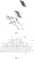
- FIG. 1 is a schematic exploded diagram of a structure of a circuit board assembly according to an embodiment of this application.
- This embodiment of this application provides a circuit board assembly 100, including a circuit board 1, a backing plate 2, one or more electronic elements 3, and a board-to-board connector 4.
- the electronic elements 3 in this embodiment of this application may include one or more electronic elements.
- FIG. 2 is a sectional drawing of a structure of a circuit board assembly according to an embodiment of this application.
- the backing plate 2 is fixedly connected to one side of the circuit board 1.
- the backing plate 2 may be fastened to one side of the circuit board 1 through welding, and the backing plate 2 is provided with an accommodation portion 21.
- the electronic element 3 is accommodated in the accommodation portion 21 and connected to the circuit board 1.
- the electronic element 3 may be welded to the circuit board 1, so that not only the electronic element 3 can be fastened, but also the electronic element 3 can be electrically connected to the circuit board 1.
- the board-to-board connector 4 is fixedly connected to one side that is of the backing plate 2 and that is away from the circuit board 1.
- the board-to-board connector 4 may be fastened to the circuit board 1 through welding.
- the electronic element 3 may be a filtering element, such as an electronic element having a function of a capacitive component, a resistive component, a common-mode inductor, or a protection diode (such as a TVS), used for the board-to-board connector 4.
- a filtering element such as an electronic element having a function of a capacitive component, a resistive component, a common-mode inductor, or a protection diode (such as a TVS), used for the board-to-board connector 4.
- a filtering element such as an electronic element having a function of a capacitive component, a resistive component, a common-mode inductor, or a protection diode (such as a TVS)
- the accommodation portion 21 may be a through via provided on the backing plate 2, the through via passes through the backing plate 2 along the height direction H of the circuit board assembly 100, and the board-to-board connector 4 covers the through via.
- the through via is made on the backing plate 2
- the electronic element 3 is disposed in the through via, and the electronic element 3 may be welded to the circuit board 1, so that the electronic element 3 can be fixedly connected to the circuit board 1, and can also be electrically connected to the circuit board 1.
- the process of making the through via on the backing plate 2 is simple and can be implemented conveniently.
- the electronic element 3 may include an electronic element having a function of a capacitive component, a resistive component, a common-mode inductor, or a protection diode (such as a TVS). According to an actual design requirement, some of these electronic elements may be disposed in the accommodation portion 21, or all of these electronic elements may be disposed in the accommodation portion 21. This is not limited herein.
- FIG. 3 is a sectional drawing of a structure of a circuit board assembly according to another embodiment of this application.
- an accommodation portion 21 may be a blind via provided on the backing plate 2, and the blind via is recessed from one side that is of the backing plate 2 and that is close to the circuit board 1 to one side close to the board-to-board connector 4.
- the accommodation portion 21 does not pass through the backing plate 2.
- This structure can shield the electronic element to a certain extent, and is applicable to an electronic element with a shielding requirement.
- FIG. 4 is a sectional drawing of a structure of a circuit board assembly according to still another embodiment of this application.
- an inner wall of the accommodation portion 21 may be provided with a shield layer 211.
- the shield layer 211 is provided to further shield the electronic element 3, thereby improving a filtering effect of a filtering component.
- the shield layer 211 may be formed by plating gold and nickel on a copper layer.
- a first soldering pad 5 is disposed between the circuit board 1 and the electronic element 3, and the electronic element 3 is fastened and electrically connected to the circuit board 1 by using the first soldering pad 5.
- the first soldering pad 5 may be a soldering pad of an electronic shielding component.
- the first soldering pad 5 is disposed so that the electronic element 3 can be fastened and electrically connected to the circuit board 1.
- the first soldering pad 5 can further enable the electronic element 3 not to interfere with work of another component.
- a second soldering pad 6 may be further disposed between the backing plate 2 and the board-to-board connector 4, and the board-to-board connector 4 is fixedly connected to the backing plate 2 by using the second soldering pad 6.
- the second soldering pad 6 is disposed so that the board-to-board connector 4 can be further elevated, thereby further providing larger accommodation space for the electronic element 3.
- the backing plate 2 is provided with a first via 22, an inner wall of the first via 22 is provided with a first conductive layer 23, the first conductive layer 23 is electrically connected to the board-to-board connector 4 by using the second soldering pad 6, and the first conductive layer 23 is electrically connected to the circuit board 1.
- the first conductive layer 23 is provided to facilitate electrical connection between the board-to-board connector 4 and the circuit board 1.
- copper may be plated in the first via 22 to form the first conductive layer 23.
- the first conductive layer 23 may be electrically connected to the second soldering pad 6, so that the first conductive layer 23 can be electrically connected to the board-to-board connector 4.
- the first conductive layer 23 may also be connected to the circuit board 1 by using a soldering pad or in another manner. This is not limited herein.
- the circuit board 1 is provided with a second via 11, an inner wall of the second via 11 is provided with a second conductive layer 12, and the second conductive layer 12 is electrically connected to the electronic element 3.
- the second via 11 and the second conductive layer 12 are provided so that the electronic element 3 can be led out to be connected to another related component, so as to meet a design requirement of a circuit. Copper may be plated in the second via 11 to form the second conductive layer 12.
- the first conductive layer 23 is provided to facilitate electrical connection between the board-to-board connector 4 and the circuit board 1.
- the first conductive layer 23 may be connected to the board-to-board connector 4 by using the second soldering pad 6 and connected to the circuit board 1 and the electronic element 3 by using the second conductive layer 12.
- the circuit board 1 is provided with a third via 13, the third via 13 communicates with the first via 22, an inner wall of the third via 13 is provided with a third conductive layer 14, and the third conductive layer 14 is electrically connected to the first conductive layer 23.
- the circuit board 1 is further provided with a fourth conductive layer 15, and the fourth conductive layer 15 is electrically connected to the third conductive layer 14 and the second conductive layer 12 separately.
- Copper may be plated in the third via 13 to form the third conductive layer 14.
- the fourth conductive layer 15 may be buried in the circuit board 1, to electrically connect the third conductive layer 14 to the second conductive layer 12.
- the board-to-board connector 4 is connected to the first soldering pad 5 by using the second soldering pad 6, the first conductive layer 23, the third conductive layer 14, the fourth conductive layer 15, and the second conductive layer 12.
- a board-to-board connector of another circuit board assembly is connected to the board-to-board connector 4 in the embodiment shown in FIG. 4 , so that the another circuit board assembly can be connected to the circuit board assembly 100 in the embodiment shown in FIG. 4 .
- FIG. 5 is a sectional drawing of a structure of a circuit board assembly according to yet another embodiment of this application.
- an accommodation portion 21 of the backing plate 2 of the circuit board assembly 100 is a through via, and is applicable to an electronic device without a shielding requirement.
- the circuit board assembly 100 may also include a first soldering pad 5 and/or a second soldering pad 6.
- a structure and a form of the first soldering pad 5 and the second soldering pad 6 may be the same as those in the embodiment shown in FIG. 4 , and details are not described herein again.
- the backing plate 2 may also be provided with a first via 22, an inner wall of the first via 22 is provided with a first conductive layer 23, and the first conductive layer 23 may be electrically connected to the first soldering pad 5.
- FIG. 6 is a sectional drawing of a structure of a circuit board assembly according to still yet another embodiment of this application.
- the circuit board assembly 200 provided in this embodiment of this application includes a circuit board 10, a board-to-board connector 20, and an electronic element 30.
- the board-to-board connector 20 is electrically connected to the circuit board 10.
- the board-to-board connector 20 includes a body 201 and a conductive portion 202.
- An accommodation portion 201a is provided inside the body 201, the conductive portion 202 is embedded in the body 201, the electronic element 30 is connected to the circuit board 10, and the electronic element 30 is accommodated in the accommodation portion 201a.
- the board-to-board connector 20 is electrically connected to the circuit board 10 by using the conductive portion 202, or may be electrically connected to a board-to-board connector in another circuit board assembly by using the conductive portion 202.
- the body 201 is a plastic body
- the conductive portion 202 is a metal spring
- the metal spring is embedded in the plastic body.
- a height of the body 201 may be increased, so that the body has space for disposing the accommodation portion 201a.
- the accommodation portion 201a may be a groove or a through groove provided on the body 201.
- the accommodation portion 201a is an internal through groove provided at a central position of the body 201, and the electronic element 30 is accommodated in the accommodation portion 201a and connected to the circuit board 10
- FIG. 6 is merely an example, and the electronic element 30 and the circuit board 10 may also be connected by providing a structure such as a soldering pad or a conductive layer.
- a shield layer may also be provided according to a design requirement of a circuit board.
- An embodiment of this application further provides an electronic device, including more than two circuit board assemblies.
- Each of the more than two circuit board assemblies includes a board-to-board connector, and the more than two circuit board assemblies are connected by using respective board-to-board connectors.
- At least one circuit board assembly is the circuit board assembly provided in any embodiment of this application.
- the electronic device may be a mobile phone.
- a circuit board assembly includes a mainboard and a board-to-board connector that cooperates with the mainboard, and another circuit board assembly includes a drive circuit board of a camera and a board-to-board connector that cooperates with the drive circuit board.
- the two board-to-board connectors cooperate with each other to implement connection between the mainboard and the drive circuit board of the camera.
- at least one circuit board assembly is the circuit board assembly provided in the embodiments of this application, so that the at least one circuit board assembly saves space occupied by an electronic element, thereby facilitating miniaturization and thinning of the mobile phone.
Landscapes
- Engineering & Computer Science (AREA)
- Microelectronics & Electronic Packaging (AREA)
- Physics & Mathematics (AREA)
- Electromagnetism (AREA)
- Combinations Of Printed Boards (AREA)
- Shielding Devices Or Components To Electric Or Magnetic Fields (AREA)
- Structures For Mounting Electric Components On Printed Circuit Boards (AREA)
Abstract
Description
- This application claims priority to
Chinese Patent Application No. 201911232961.4, filed with the Chinese Patent Office on December 5, 2019 - This application relates to the field of electronic component technologies, and in particular, to a circuit board assembly and an electronic device.
- A printed circuit board (Printed Circuit Board, PCB) is an important part in an electronic product, and printed circuit boards may be connected by using a board-to-board connector (Board-to-board connectors, BTB).
- Many electronic elements are disposed on the periphery of the board-to-board connector for functions such as filtering. After the board-to-board connector is connected to the printed circuit board, these electronic elements are disposed on a surface of the printed circuit board and surround the board-to-board connector. During actual production, assembly, and repair at a service center, the electronic elements are easily damaged due to impact, and consequently poor functions are caused.
- An objective of this application is to provide a circuit board assembly and an electronic device, so that peripheral electronic elements are not damaged by impact during production, assembly or repair of the board-to-board connector.
- According to a first aspect, a circuit board assembly is provided, including:
- a circuit board;
- a backing plate fixedly connected to one side of the circuit board, where the backing plate is provided with an accommodation portion;
- an electronic element accommodated in the accommodation portion and connected to the circuit board; and
- a board-to-board connector fixedly connected to one side that is of the backing plate and that is away from the circuit board.
- The accommodation portion is provided on the backing plate, and the electronic element is accommodated in the accommodation portion, so that the electronic element is located in the space under the board-to-board connector. Therefore, not only damage caused by impact of the electronic element can be prevented, but also space of the circuit board assembly can be greatly saved.
- In a possible implementation, the accommodation portion is a through via provided on the backing plate, and the through via passes through along a height direction of the circuit board assembly; and
the board-to-board connector covers the through via. - The through via is made on the backing plate, and the electronic element is disposed in the through via and connected to the circuit board. The process of making the through via on the backing plate is simple and can be implemented conveniently.
- In a possible implementation, the accommodation portion is a blind via provided on the backing plate, and the blind via is recessed from one side that is of the backing plate and that is close to the circuit board to one side close to the board-to-board connector.
- The accommodation portion is arranged as the blind via, so that the electronic element can be shielded to a certain extent, which is applicable to an electronic element with a shielding requirement.
- In a possible implementation, an inner wall of the accommodation portion is provided with a shield layer. The shield layer is provided so that the electronic element can be further shielded.
- The shield layer may be formed by plating gold and nickel on a copper layer.
- In a possible implementation, a first soldering pad is further included, where the electronic element is fastened and electrically connected to the circuit board by using the first soldering pad. The first soldering pad may be a soldering pad of an electronic shielding component, so that the electronic element does not interfere with work of another component.
- In a possible implementation, a second soldering pad is further included, where the board-to-board connector is fixedly connected to the backing plate by using the second soldering pad. The second soldering pad is disposed so that the board-to-board connector can be further elevated, thereby further providing larger accommodation space for the electronic element.
- In a possible implementation, the backing plate is provided with a first via, an inner wall of the first via is provided with a first conductive layer, the first conductive layer is electrically connected to the board-to-board connector by using the second soldering pad, and the first conductive layer is electrically connected to the circuit board. The first conductive layer is provided to facilitate electrical connection between the board-to-board connector and the circuit board.
- Copper may be plated in the first via to form the first conductive layer.
- In a possible implementation, the circuit board is provided with a second via, and an inner wall of the second via is provided with a second conductive layer; and
the second conductive layer is electrically connected to the electronic element. - The second via and the second conductive layer are provided so that the electronic element can be led out to be connected to another related component, so as to meet a design requirement of a circuit.
- Copper may be plated in the second via to form the second conductive layer.
- In a possible implementation, the circuit board is provided with a third via, and the third via communicates with the first via;
- an inner wall of the third via is provided with a third conductive layer, and the third conductive layer is electrically connected to the first conductive layer; and
- the circuit board is further provided with a fourth conductive layer, and the fourth conductive layer is electrically connected to the third conductive layer and the second conductive layer separately.
- Copper may be plated in the third via to form the third conductive layer. The fourth conductive layer may be buried in the circuit board, to electrically connect the third conductive layer to the second conductive layer.
- According to a second aspect, a circuit board assembly is provided, including:
- a circuit board;
- a board-to-board connector, where the board-to-board connector is connected to the circuit board, and the board-to-board connector includes:
- a body, where an accommodation portion is provided inside the body; and
- a conductive portion embedded in the body; and
- an electronic element, where the electronic element is connected to the circuit board, and the electronic element is accommodated in the accommodation portion.
- In the circuit board assembly and the electronic device provided in this application, the electronic element is accommodated in the accommodation portion, and the accommodation portion is provided in the body of the board-to-board connector, so that the electronic element is located in the space under the board-to-board connector. Therefore, not only damage caused by impact of the electronic element can be prevented, but also space of the circuit board assembly can be greatly saved.
- According to a third aspect, an electronic device is provided, including more than two circuit board assemblies, where each of the more than two circuit board assemblies includes a board-to-board connector, the more than two circuit board assemblies are connected by using respective board-to-board connectors, and at least one circuit board assembly is the circuit board assembly provided in this application.
- At least one circuit board assembly is arranged as the circuit board assembly provided in this application, so that the at least one circuit board assembly saves space occupied by an electronic element, thereby facilitating miniaturization and thinning of a mobile phone.
- The technical solutions provided in this application may achieve the following beneficial effects:
- In the circuit board assembly and the electronic device provided in this application, the electronic element is accommodated in the accommodation portion, and the accommodation portion may be provided on the backing plate, or may be provided in the body of the board-to-board connector, so that the electronic element is located in the space under the board-to-board connector. Therefore, not only damage caused by impact of the electronic element can be prevented, but also space of the circuit board assembly can be greatly saved, thereby facilitating miniaturization and thinning of the electronic device.
-
-
FIG. 1 is a schematic exploded diagram of a structure of a circuit board assembly according to an embodiment of this application; -
FIG. 2 is a sectional drawing of a structure of a circuit board assembly according to an embodiment of this application; -
FIG. 3 is a sectional drawing of a structure of a circuit board assembly according to another embodiment of this application; -
FIG. 4 is a sectional drawing of a structure of a circuit board assembly according to still another embodiment of this application; -
FIG. 5 is a sectional drawing of a structure of a circuit board assembly according to yet another embodiment of this application; and -
FIG. 6 is a sectional drawing of a structure of a circuit board assembly according to still yet another embodiment of this application. -
- 100: Circuit board assembly;
- Circuit board;
- 11: Second via;
- 12: Second conductive layer;
- 13: Third via;
- 14: Third conductive layer;
- 15: Fourth conductive layer;
- 2: Backing plate;
- 21: Accommodation portion;
- 211: Shield layer;
- 22: First via;
- 23: First conductive layer;
- 3: Electronic element;
- 4: Board-to-board connector;
- 5: First soldering pad;
- 6: Second soldering pad;
- 200: Circuit board assembly;
- 10: Circuit board;
- 20: Board-to-board connector;
- 201: Body;
- 201a: Accommodation portion;
- 202: Conductive portion;
- 30: Electronic element.
- The terms used in the embodiments of this application are merely for the purpose of illustrating specific embodiments, and are not intended to limit this application. The terms "a", "said" and "the" of singular forms used in the embodiments and the appended claims of this application are also intended to include plural forms, unless otherwise specified in the context clearly.
- It should be understood that the term "and/or" in this specification describes only an association relationship for describing associated objects and represents that three relationships may exist. For example, A and/or B may represent the following three cases: Only A exists, both A and B exist, and only B exists. In addition, the character "/" in this specification generally indicates an "or" relationship between the associated objects.
- It should be noted that, direction terms such as "top", "bottom", "left", and "right" described in the embodiments of this application are described from an angle shown in the accompanying drawings, and should not be construed as a limitation to the embodiments of this application. In addition, in the context, it should be further noted that, when it is mentioned that an element is connected to the "top" or "bottom" of another element, the element cannot only be directly connected to the "top" or "bottom" of the another element, but may also be indirectly connected to the "top" or "bottom" of the another element by using an intermediate element.
- An embodiment of this application provides an electronic device. The electronic device may be a mobile phone, a tablet computer, or another electronic product. These electronic devices usually include mainboards. A mobile phone is used as an example, a mainboard may be connected to a circuit board of a component such as a camera, a battery, or a USB by using a board-to-board connector, and other circuit boards may also be connected by using board-to-board connectors. An electronic element such as a capacitor, an inductor, or a resistor is disposed on the periphery of the board-to-board connector. With deeper development of an integrated and miniaturized design of the mobile phone, layout space of the mainboard or other circuit boards becomes increasingly limited, and these electronic elements are easily damaged by impact during assembly or repair. A circuit board assembly and the electronic device provided in the embodiments of this application can resolve the technical problem that layout space of a circuit board is limited and electronic elements are damaged.
- An embodiment of this application provides an electronic device, including more than two circuit board assemblies, where one circuit board assembly may include a mainboard of the electronic device, and other circuit board assemblies may include other circuit boards on the electronic device.
- Each of the more than two circuit board assemblies may include a board-to-board connector, and the more than two circuit board assemblies are connected by using respective board-to-board connectors. At least one circuit board assembly is the circuit board assembly provided in any embodiment of this application.
- In other words, in the electronic device provided in this embodiment of this application, at least one circuit board assembly has a compact layout structure, so that space occupied by electronic elements can be reduced, thereby implementing miniaturization and thinning of the electronic device, and preventing the electronic elements from being damaged by impact during assembly and repair.
-
FIG. 1 is a schematic exploded diagram of a structure of a circuit board assembly according to an embodiment of this application. This embodiment of this application provides acircuit board assembly 100, including acircuit board 1, abacking plate 2, one or moreelectronic elements 3, and a board-to-board connector 4. Theelectronic elements 3 in this embodiment of this application may include one or more electronic elements. -
FIG. 2 is a sectional drawing of a structure of a circuit board assembly according to an embodiment of this application. Referring to thecircuit board assembly 100 inFIG. 1 and FIG. 2 , thebacking plate 2 is fixedly connected to one side of thecircuit board 1. In a possible implementation, thebacking plate 2 may be fastened to one side of thecircuit board 1 through welding, and thebacking plate 2 is provided with anaccommodation portion 21. - The
electronic element 3 is accommodated in theaccommodation portion 21 and connected to thecircuit board 1. In a possible implementation, theelectronic element 3 may be welded to thecircuit board 1, so that not only theelectronic element 3 can be fastened, but also theelectronic element 3 can be electrically connected to thecircuit board 1. - The board-to-
board connector 4 is fixedly connected to one side that is of thebacking plate 2 and that is away from thecircuit board 1. In a possible implementation, the board-to-board connector 4 may be fastened to thecircuit board 1 through welding. - The
electronic element 3 may be a filtering element, such as an electronic element having a function of a capacitive component, a resistive component, a common-mode inductor, or a protection diode (such as a TVS), used for the board-to-board connector 4. In a height direction H inFIG. 2 , theelectronic element 3 is accommodated in the interior space (namely, the accommodation portion 21) of thebacking plate 2 under the board-to-board connector 4. Therefore, not only damage caused by impact of theelectronic element 3 can be prevented, but also space of thecircuit board assembly 100 can be greatly saved. - As shown in
FIG. 2 , in a specific implementation, theaccommodation portion 21 may be a through via provided on thebacking plate 2, the through via passes through thebacking plate 2 along the height direction H of thecircuit board assembly 100, and the board-to-board connector 4 covers the through via. - In this embodiment, the through via is made on the
backing plate 2, theelectronic element 3 is disposed in the through via, and theelectronic element 3 may be welded to thecircuit board 1, so that theelectronic element 3 can be fixedly connected to thecircuit board 1, and can also be electrically connected to thecircuit board 1. The process of making the through via on thebacking plate 2 is simple and can be implemented conveniently. Theelectronic element 3 may include an electronic element having a function of a capacitive component, a resistive component, a common-mode inductor, or a protection diode (such as a TVS). According to an actual design requirement, some of these electronic elements may be disposed in theaccommodation portion 21, or all of these electronic elements may be disposed in theaccommodation portion 21. This is not limited herein. -
FIG. 3 is a sectional drawing of a structure of a circuit board assembly according to another embodiment of this application. As shown inFIG. 3 , in a specific implementation, anaccommodation portion 21 may be a blind via provided on thebacking plate 2, and the blind via is recessed from one side that is of thebacking plate 2 and that is close to thecircuit board 1 to one side close to the board-to-board connector 4. - In other words, in a height direction of the
circuit board assembly 100, theaccommodation portion 21 does not pass through thebacking plate 2. This structure can shield the electronic element to a certain extent, and is applicable to an electronic element with a shielding requirement. -
FIG. 4 is a sectional drawing of a structure of a circuit board assembly according to still another embodiment of this application. As shown inFIG. 4 , in a specific implementation, an inner wall of theaccommodation portion 21 may be provided with ashield layer 211. Theshield layer 211 is provided to further shield theelectronic element 3, thereby improving a filtering effect of a filtering component. Theshield layer 211 may be formed by plating gold and nickel on a copper layer. - Still referring to
FIG. 4 , in a specific implementation, afirst soldering pad 5 is disposed between thecircuit board 1 and theelectronic element 3, and theelectronic element 3 is fastened and electrically connected to thecircuit board 1 by using thefirst soldering pad 5. Thefirst soldering pad 5 may be a soldering pad of an electronic shielding component. Thefirst soldering pad 5 is disposed so that theelectronic element 3 can be fastened and electrically connected to thecircuit board 1. In addition, thefirst soldering pad 5 can further enable theelectronic element 3 not to interfere with work of another component. - Still referring to
FIG. 4 , in a specific implementation, asecond soldering pad 6 may be further disposed between thebacking plate 2 and the board-to-board connector 4, and the board-to-board connector 4 is fixedly connected to thebacking plate 2 by using thesecond soldering pad 6. Thesecond soldering pad 6 is disposed so that the board-to-board connector 4 can be further elevated, thereby further providing larger accommodation space for theelectronic element 3. - In a specific implementation, the
backing plate 2 is provided with a first via 22, an inner wall of the first via 22 is provided with a firstconductive layer 23, the firstconductive layer 23 is electrically connected to the board-to-board connector 4 by using thesecond soldering pad 6, and the firstconductive layer 23 is electrically connected to thecircuit board 1. The firstconductive layer 23 is provided to facilitate electrical connection between the board-to-board connector 4 and thecircuit board 1. For example, copper may be plated in the first via 22 to form the firstconductive layer 23. - Specifically, the first
conductive layer 23 may be electrically connected to thesecond soldering pad 6, so that the firstconductive layer 23 can be electrically connected to the board-to-board connector 4. The firstconductive layer 23 may also be connected to thecircuit board 1 by using a soldering pad or in another manner. This is not limited herein. - In a specific implementation, the
circuit board 1 is provided with a second via 11, an inner wall of the second via 11 is provided with a secondconductive layer 12, and the secondconductive layer 12 is electrically connected to theelectronic element 3. - The second via 11 and the second
conductive layer 12 are provided so that theelectronic element 3 can be led out to be connected to another related component, so as to meet a design requirement of a circuit. Copper may be plated in the second via 11 to form the secondconductive layer 12. - As mentioned above, the first
conductive layer 23 is provided to facilitate electrical connection between the board-to-board connector 4 and thecircuit board 1. The firstconductive layer 23 may be connected to the board-to-board connector 4 by using thesecond soldering pad 6 and connected to thecircuit board 1 and theelectronic element 3 by using the secondconductive layer 12. - In a specific implementation, the
circuit board 1 is provided with a third via 13, the third via 13 communicates with the first via 22, an inner wall of the third via 13 is provided with a thirdconductive layer 14, and the thirdconductive layer 14 is electrically connected to the firstconductive layer 23. Thecircuit board 1 is further provided with a fourthconductive layer 15, and the fourthconductive layer 15 is electrically connected to the thirdconductive layer 14 and the secondconductive layer 12 separately. - Copper may be plated in the third via 13 to form the third
conductive layer 14. The fourthconductive layer 15 may be buried in thecircuit board 1, to electrically connect the thirdconductive layer 14 to the secondconductive layer 12. In the embodiment shown inFIG. 4 , the board-to-board connector 4 is connected to thefirst soldering pad 5 by using thesecond soldering pad 6, the firstconductive layer 23, the thirdconductive layer 14, the fourthconductive layer 15, and the secondconductive layer 12. - During use, a board-to-board connector of another circuit board assembly is connected to the board-to-
board connector 4 in the embodiment shown inFIG. 4 , so that the another circuit board assembly can be connected to thecircuit board assembly 100 in the embodiment shown inFIG. 4 . -
FIG. 5 is a sectional drawing of a structure of a circuit board assembly according to yet another embodiment of this application. In the embodiment shown inFIG. 5 , anaccommodation portion 21 of thebacking plate 2 of thecircuit board assembly 100 is a through via, and is applicable to an electronic device without a shielding requirement. In this embodiment, thecircuit board assembly 100 may also include afirst soldering pad 5 and/or asecond soldering pad 6. A structure and a form of thefirst soldering pad 5 and thesecond soldering pad 6 may be the same as those in the embodiment shown inFIG. 4 , and details are not described herein again. - The
backing plate 2 may also be provided with a first via 22, an inner wall of the first via 22 is provided with a firstconductive layer 23, and the firstconductive layer 23 may be electrically connected to thefirst soldering pad 5. -
FIG. 6 is a sectional drawing of a structure of a circuit board assembly according to still yet another embodiment of this application. As shown inFIG. 6 , thecircuit board assembly 200 provided in this embodiment of this application includes acircuit board 10, a board-to-board connector 20, and anelectronic element 30. The board-to-board connector 20 is electrically connected to thecircuit board 10. The board-to-board connector 20 includes abody 201 and aconductive portion 202. Anaccommodation portion 201a is provided inside thebody 201, theconductive portion 202 is embedded in thebody 201, theelectronic element 30 is connected to thecircuit board 10, and theelectronic element 30 is accommodated in theaccommodation portion 201a. - The board-to-
board connector 20 is electrically connected to thecircuit board 10 by using theconductive portion 202, or may be electrically connected to a board-to-board connector in another circuit board assembly by using theconductive portion 202. In this embodiment, thebody 201 is a plastic body, theconductive portion 202 is a metal spring, and the metal spring is embedded in the plastic body. - In this embodiment, a height of the
body 201 may be increased, so that the body has space for disposing theaccommodation portion 201a. Theaccommodation portion 201a may be a groove or a through groove provided on thebody 201. In the embodiment shown inFIG. 6 , theaccommodation portion 201a is an internal through groove provided at a central position of thebody 201, and theelectronic element 30 is accommodated in theaccommodation portion 201a and connected to thecircuit board 10 - It may be understood that the embodiment shown in
FIG. 6 is merely an example, and theelectronic element 30 and thecircuit board 10 may also be connected by providing a structure such as a soldering pad or a conductive layer. A shield layer may also be provided according to a design requirement of a circuit board. - An embodiment of this application further provides an electronic device, including more than two circuit board assemblies. Each of the more than two circuit board assemblies includes a board-to-board connector, and the more than two circuit board assemblies are connected by using respective board-to-board connectors. At least one circuit board assembly is the circuit board assembly provided in any embodiment of this application.
- In a specific implementation, the electronic device may be a mobile phone. A circuit board assembly includes a mainboard and a board-to-board connector that cooperates with the mainboard, and another circuit board assembly includes a drive circuit board of a camera and a board-to-board connector that cooperates with the drive circuit board. The two board-to-board connectors cooperate with each other to implement connection between the mainboard and the drive circuit board of the camera. In the two circuit board assemblies, at least one circuit board assembly is the circuit board assembly provided in the embodiments of this application, so that the at least one circuit board assembly saves space occupied by an electronic element, thereby facilitating miniaturization and thinning of the mobile phone.
- It should be noted that a part of the present patent application document includes copyright-protected content. The copyright owner retains the copyright except for making copies of patent documents or recorded patent document content in the Patent Office.
Claims (11)
- A circuit board assembly, comprising:a circuit board (1);a backing plate (2) fixedly connected to one side of the circuit board (1), wherein the backing plate (2) is provided with an accommodation portion (21);an electronic element (3) accommodated in the accommodation portion (21) and connected to the circuit board (1); anda board-to-board connector (4) fixedly connected to one side that is of the backing plate (2) and that is away from the circuit board (1).
- The circuit board assembly according to claim 1, wherein the accommodation portion (21) is a through via provided on the backing plate (2), and the through via passes through along a height direction of the circuit board assembly; and
the board-to-board connector (4) covers the through via. - The circuit board assembly according to claim 1, wherein the accommodation portion (21) is a blind via provided on the backing plate (2), and the blind via is recessed from one side that is of the backing plate (2) and that is close to the circuit board (1) to one side close to the board-to-board connector (4).
- The circuit board assembly according to claim 3, wherein an inner wall of the accommodation portion (21) is provided with a shield layer (211).
- The circuit board assembly according to claim 1, further comprising a first soldering pad (5), wherein the electronic element (3) is fastened and electrically connected to the circuit board (1) by using the first soldering pad (5).
- The circuit board assembly according to claim 1, further comprising a second soldering pad (6), wherein the board-to-board connector (4) is fixedly connected to the backing plate (2) by using the second soldering pad (6).
- The circuit board assembly according to claim 6, wherein the backing plate (2) is provided with a first via (22), an inner wall of the first via (22) is provided with a first conductive layer (23), the first conductive layer (23) is electrically connected to the board-to-board connector (4) by using the second soldering pad (6), and the first conductive layer (23) is electrically connected to the circuit board (1).
- The circuit board assembly according to claim 7, wherein the circuit board (1) is provided with a second via (11), and an inner wall of the second via (11) is provided with a second conductive layer (12); and
the second conductive layer (12) is electrically connected to the electronic element (3). - The circuit board assembly according to claim 8, wherein the circuit board (1) is provided with a third via (13), and the third via (13) communicates with the first via (22);an inner wall of the third via (13) is provided with a third conductive layer (14), and the third conductive layer (14) is electrically connected to the first conductive layer (23); andthe circuit board (1) is further provided with a fourth conductive layer (15), and the fourth conductive layer (15) is electrically connected to the third conductive layer (14) and the second conductive layer (12) separately.
- A circuit board assembly, comprising:a circuit board (10);a board-to-board connector (20), wherein the board-to-board connector (20) is electrically connected to the circuit board (10), and the board-to-board connector (20) comprises:a body (201), wherein an accommodation portion (201a) is provided inside the body; anda conductive portion (202), wherein the conductive portion (202) is embedded in the body (201); andan electronic element (30), wherein the electronic element (30) is connected to the circuit board (10), and the electronic element (30) is accommodated in the accommodation portion (201a).
- An electronic device, comprising more than two circuit board assemblies, wherein each of the more than two circuit board assemblies comprises a board-to-board connector, the more than two circuit board assemblies are connected by using respective board-to-board connectors, and at least one circuit board assembly is the circuit board assembly according to any one of claims 1 to 10.
Priority Applications (1)
| Application Number | Priority Date | Filing Date | Title |
|---|---|---|---|
| EP24164750.2A EP4425717B1 (en) | 2019-12-05 | 2020-11-11 | Circuit board assembly and electronic device |
Applications Claiming Priority (2)
| Application Number | Priority Date | Filing Date | Title |
|---|---|---|---|
| CN201911232961.4A CN112930030B (en) | 2019-12-05 | 2019-12-05 | Circuit board assembly and electronic equipment |
| PCT/CN2020/128169 WO2021109818A1 (en) | 2019-12-05 | 2020-11-11 | Circuit board assembly and electronic apparatus |
Related Child Applications (2)
| Application Number | Title | Priority Date | Filing Date |
|---|---|---|---|
| EP24164750.2A Division EP4425717B1 (en) | 2019-12-05 | 2020-11-11 | Circuit board assembly and electronic device |
| EP24164750.2A Division-Into EP4425717B1 (en) | 2019-12-05 | 2020-11-11 | Circuit board assembly and electronic device |
Publications (3)
| Publication Number | Publication Date |
|---|---|
| EP4007457A1 true EP4007457A1 (en) | 2022-06-01 |
| EP4007457A4 EP4007457A4 (en) | 2023-02-08 |
| EP4007457B1 EP4007457B1 (en) | 2024-05-01 |
Family
ID=76161018
Family Applications (2)
| Application Number | Title | Priority Date | Filing Date |
|---|---|---|---|
| EP20897277.8A Active EP4007457B1 (en) | 2019-12-05 | 2020-11-11 | Circuit board assembly and electronic apparatus |
| EP24164750.2A Active EP4425717B1 (en) | 2019-12-05 | 2020-11-11 | Circuit board assembly and electronic device |
Family Applications After (1)
| Application Number | Title | Priority Date | Filing Date |
|---|---|---|---|
| EP24164750.2A Active EP4425717B1 (en) | 2019-12-05 | 2020-11-11 | Circuit board assembly and electronic device |
Country Status (3)
| Country | Link |
|---|---|
| EP (2) | EP4007457B1 (en) |
| CN (1) | CN112930030B (en) |
| WO (1) | WO2021109818A1 (en) |
Families Citing this family (2)
| Publication number | Priority date | Publication date | Assignee | Title |
|---|---|---|---|---|
| CN115707173B (en) * | 2021-08-16 | 2025-09-12 | 宏启胜精密电子(秦皇岛)有限公司 | Circuit board assembly with shielding effect and manufacturing method thereof |
| CN117119843B (en) * | 2023-04-14 | 2024-05-17 | 荣耀终端有限公司 | Electronic device and method of manufacturing the same |
Family Cites Families (14)
| Publication number | Priority date | Publication date | Assignee | Title |
|---|---|---|---|---|
| US5309324A (en) * | 1991-11-26 | 1994-05-03 | Herandez Jorge M | Device for interconnecting integrated circuit packages to circuit boards |
| JP3718161B2 (en) * | 2001-11-22 | 2005-11-16 | ヒロセ電機株式会社 | Electronic component assembly and unit body therefor |
| JP4186843B2 (en) * | 2004-03-03 | 2008-11-26 | 松下電器産業株式会社 | Three-dimensional electronic circuit device |
| CN2699531Y (en) * | 2004-03-03 | 2005-05-11 | 富士康(昆山)电脑接插件有限公司 | Electric connector |
| WO2006057424A1 (en) * | 2004-11-24 | 2006-06-01 | Matsushita Electric Industrial Co., Ltd. | Connector with shield, and circuit board device |
| JP5736227B2 (en) * | 2011-04-22 | 2015-06-17 | 第一電子工業株式会社 | Board to board connector |
| KR101586235B1 (en) * | 2014-06-03 | 2016-01-18 | (주)우주일렉트로닉스 | Board to board connector |
| CN204045775U (en) * | 2014-08-04 | 2014-12-24 | 昆山科信成电子有限公司 | There is the miniature Substrate-substrate connector combination of heat sinking function |
| KR102288437B1 (en) * | 2014-11-21 | 2021-08-10 | 삼성전자주식회사 | A foldable electronic device |
| DE102015221146A1 (en) * | 2015-10-29 | 2017-05-04 | Conti Temic Microelectronic Gmbh | Electronic component and method for producing an electronic component |
| CN105828530B (en) * | 2015-10-30 | 2019-02-15 | 维沃移动通信有限公司 | A circuit board and electronic equipment |
| CN205282690U (en) * | 2015-12-22 | 2016-06-01 | 莫仕连接器(成都)有限公司 | Electric connector |
| US10424345B1 (en) * | 2018-06-11 | 2019-09-24 | Western Digital Technologies, Inc. | Misalignment-tolerant flexible type electrical feed-through |
| CN209329278U (en) * | 2019-01-17 | 2019-08-30 | 歌尔科技有限公司 | A kind of sealing device and board to board connector |
-
2019
- 2019-12-05 CN CN201911232961.4A patent/CN112930030B/en active Active
-
2020
- 2020-11-11 WO PCT/CN2020/128169 patent/WO2021109818A1/en not_active Ceased
- 2020-11-11 EP EP20897277.8A patent/EP4007457B1/en active Active
- 2020-11-11 EP EP24164750.2A patent/EP4425717B1/en active Active
Also Published As
| Publication number | Publication date |
|---|---|
| EP4425717A3 (en) | 2024-11-06 |
| EP4425717B1 (en) | 2025-09-03 |
| CN112930030B (en) | 2022-09-23 |
| EP4007457A4 (en) | 2023-02-08 |
| CN112930030A (en) | 2021-06-08 |
| EP4425717A2 (en) | 2024-09-04 |
| WO2021109818A1 (en) | 2021-06-10 |
| EP4007457B1 (en) | 2024-05-01 |
Similar Documents
| Publication | Publication Date | Title |
|---|---|---|
| JP5041897B2 (en) | Inductor-formed wiring board with shielding function | |
| KR20190124280A (en) | Motherboards and Terminals for Consumer Electronics | |
| US8054639B2 (en) | Image-sensing module for reducing overall thickness thereof and preventing EMI | |
| CN210008007U (en) | Electronic device | |
| US20090135576A1 (en) | Stacking structure of printed circuit board | |
| CN115280605A (en) | Substrate connector | |
| US9553382B2 (en) | Headphone socket assembly and electronic equipment including same | |
| US20060189183A1 (en) | Camera module connector | |
| EP4425717A2 (en) | Circuit board assembly and electronic device | |
| EP2961007B1 (en) | Headphone socket assembly and electronic equipment | |
| US20210289673A1 (en) | Shielding member | |
| CN112187970B (en) | Camera module and electronic device thereof | |
| WO2018168352A1 (en) | Receptacle | |
| KR101993374B1 (en) | Connecting device for electronic components of portable terminal | |
| CN217428419U (en) | Electronic device and circuit board assembly | |
| HK40069825A (en) | Circuit board assembly and electronic apparatus | |
| US9455511B1 (en) | Circuit board connecting device | |
| HK40069825B (en) | Circuit board assembly and electronic apparatus | |
| CN109121293B (en) | Printed circuit board assembly and electronic device | |
| US8093509B2 (en) | Flexible thin image-sensing module with anti-EMI function and flexible thin PCB module with anti-EMI function | |
| US9831579B1 (en) | Adapter frame with a set of electrical pads on its top and bottom surfaces for a board-to-board connection | |
| CN108346939A (en) | Electrical connector | |
| CN106255016A (en) | A speaker feed system and mobile terminal | |
| CN224265065U (en) | electronic devices | |
| US20190082533A1 (en) | Electrical conductive module |
Legal Events
| Date | Code | Title | Description |
|---|---|---|---|
| STAA | Information on the status of an ep patent application or granted ep patent |
Free format text: STATUS: THE INTERNATIONAL PUBLICATION HAS BEEN MADE |
|
| PUAI | Public reference made under article 153(3) epc to a published international application that has entered the european phase |
Free format text: ORIGINAL CODE: 0009012 |
|
| STAA | Information on the status of an ep patent application or granted ep patent |
Free format text: STATUS: REQUEST FOR EXAMINATION WAS MADE |
|
| 17P | Request for examination filed |
Effective date: 20220222 |
|
| AK | Designated contracting states |
Kind code of ref document: A1 Designated state(s): AL AT BE BG CH CY CZ DE DK EE ES FI FR GB GR HR HU IE IS IT LI LT LU LV MC MK MT NL NO PL PT RO RS SE SI SK SM TR |
|
| REG | Reference to a national code |
Ref country code: HK Ref legal event code: DE Ref document number: 40069825 Country of ref document: HK |
|
| A4 | Supplementary search report drawn up and despatched |
Effective date: 20230110 |
|
| RIC1 | Information provided on ipc code assigned before grant |
Ipc: H01R 12/71 20110101ALN20230103BHEP Ipc: H05K 1/18 19680901AFI20230103BHEP |
|
| DAV | Request for validation of the european patent (deleted) | ||
| DAX | Request for extension of the european patent (deleted) | ||
| STAA | Information on the status of an ep patent application or granted ep patent |
Free format text: STATUS: EXAMINATION IS IN PROGRESS |
|
| 17Q | First examination report despatched |
Effective date: 20230830 |
|
| GRAP | Despatch of communication of intention to grant a patent |
Free format text: ORIGINAL CODE: EPIDOSNIGR1 |
|
| STAA | Information on the status of an ep patent application or granted ep patent |
Free format text: STATUS: GRANT OF PATENT IS INTENDED |
|
| INTG | Intention to grant announced |
Effective date: 20240123 |
|
| GRAS | Grant fee paid |
Free format text: ORIGINAL CODE: EPIDOSNIGR3 |
|
| GRAA | (expected) grant |
Free format text: ORIGINAL CODE: 0009210 |
|
| STAA | Information on the status of an ep patent application or granted ep patent |
Free format text: STATUS: THE PATENT HAS BEEN GRANTED |
|
| AK | Designated contracting states |
Kind code of ref document: B1 Designated state(s): AL AT BE BG CH CY CZ DE DK EE ES FI FR GB GR HR HU IE IS IT LI LT LU LV MC MK MT NL NO PL PT RO RS SE SI SK SM TR |
|
| REG | Reference to a national code |
Ref country code: GB Ref legal event code: FG4D |
|
| REG | Reference to a national code |
Ref country code: CH Ref legal event code: EP |
|
| REG | Reference to a national code |
Ref country code: IE Ref legal event code: FG4D |
|
| REG | Reference to a national code |
Ref country code: DE Ref legal event code: R096 Ref document number: 602020030428 Country of ref document: DE |
|
| REG | Reference to a national code |
Ref country code: NL Ref legal event code: FP |
|
| REG | Reference to a national code |
Ref country code: LT Ref legal event code: MG9D |
|
| PG25 | Lapsed in a contracting state [announced via postgrant information from national office to epo] |
Ref country code: IS Free format text: LAPSE BECAUSE OF FAILURE TO SUBMIT A TRANSLATION OF THE DESCRIPTION OR TO PAY THE FEE WITHIN THE PRESCRIBED TIME-LIMIT Effective date: 20240901 |
|
| PG25 | Lapsed in a contracting state [announced via postgrant information from national office to epo] |
Ref country code: BG Free format text: LAPSE BECAUSE OF FAILURE TO SUBMIT A TRANSLATION OF THE DESCRIPTION OR TO PAY THE FEE WITHIN THE PRESCRIBED TIME-LIMIT Effective date: 20240501 |
|
| PG25 | Lapsed in a contracting state [announced via postgrant information from national office to epo] |
Ref country code: FI Free format text: LAPSE BECAUSE OF FAILURE TO SUBMIT A TRANSLATION OF THE DESCRIPTION OR TO PAY THE FEE WITHIN THE PRESCRIBED TIME-LIMIT Effective date: 20240501 Ref country code: HR Free format text: LAPSE BECAUSE OF FAILURE TO SUBMIT A TRANSLATION OF THE DESCRIPTION OR TO PAY THE FEE WITHIN THE PRESCRIBED TIME-LIMIT Effective date: 20240501 |
|
| PG25 | Lapsed in a contracting state [announced via postgrant information from national office to epo] |
Ref country code: GR Free format text: LAPSE BECAUSE OF FAILURE TO SUBMIT A TRANSLATION OF THE DESCRIPTION OR TO PAY THE FEE WITHIN THE PRESCRIBED TIME-LIMIT Effective date: 20240802 |
|
| PG25 | Lapsed in a contracting state [announced via postgrant information from national office to epo] |
Ref country code: PT Free format text: LAPSE BECAUSE OF FAILURE TO SUBMIT A TRANSLATION OF THE DESCRIPTION OR TO PAY THE FEE WITHIN THE PRESCRIBED TIME-LIMIT Effective date: 20240902 |
|
| REG | Reference to a national code |
Ref country code: AT Ref legal event code: MK05 Ref document number: 1684146 Country of ref document: AT Kind code of ref document: T Effective date: 20240501 |
|
| PG25 | Lapsed in a contracting state [announced via postgrant information from national office to epo] |
Ref country code: ES Free format text: LAPSE BECAUSE OF FAILURE TO SUBMIT A TRANSLATION OF THE DESCRIPTION OR TO PAY THE FEE WITHIN THE PRESCRIBED TIME-LIMIT Effective date: 20240501 |
|
| PG25 | Lapsed in a contracting state [announced via postgrant information from national office to epo] |
Ref country code: AT Free format text: LAPSE BECAUSE OF FAILURE TO SUBMIT A TRANSLATION OF THE DESCRIPTION OR TO PAY THE FEE WITHIN THE PRESCRIBED TIME-LIMIT Effective date: 20240501 |
|
| PG25 | Lapsed in a contracting state [announced via postgrant information from national office to epo] |
Ref country code: PL Free format text: LAPSE BECAUSE OF FAILURE TO SUBMIT A TRANSLATION OF THE DESCRIPTION OR TO PAY THE FEE WITHIN THE PRESCRIBED TIME-LIMIT Effective date: 20240501 |
|
| PG25 | Lapsed in a contracting state [announced via postgrant information from national office to epo] |
Ref country code: LV Free format text: LAPSE BECAUSE OF FAILURE TO SUBMIT A TRANSLATION OF THE DESCRIPTION OR TO PAY THE FEE WITHIN THE PRESCRIBED TIME-LIMIT Effective date: 20240501 |
|
| PG25 | Lapsed in a contracting state [announced via postgrant information from national office to epo] |
Ref country code: PT Free format text: LAPSE BECAUSE OF FAILURE TO SUBMIT A TRANSLATION OF THE DESCRIPTION OR TO PAY THE FEE WITHIN THE PRESCRIBED TIME-LIMIT Effective date: 20240902 Ref country code: PL Free format text: LAPSE BECAUSE OF FAILURE TO SUBMIT A TRANSLATION OF THE DESCRIPTION OR TO PAY THE FEE WITHIN THE PRESCRIBED TIME-LIMIT Effective date: 20240501 Ref country code: NO Free format text: LAPSE BECAUSE OF FAILURE TO SUBMIT A TRANSLATION OF THE DESCRIPTION OR TO PAY THE FEE WITHIN THE PRESCRIBED TIME-LIMIT Effective date: 20240801 Ref country code: LV Free format text: LAPSE BECAUSE OF FAILURE TO SUBMIT A TRANSLATION OF THE DESCRIPTION OR TO PAY THE FEE WITHIN THE PRESCRIBED TIME-LIMIT Effective date: 20240501 Ref country code: IS Free format text: LAPSE BECAUSE OF FAILURE TO SUBMIT A TRANSLATION OF THE DESCRIPTION OR TO PAY THE FEE WITHIN THE PRESCRIBED TIME-LIMIT Effective date: 20240901 Ref country code: HR Free format text: LAPSE BECAUSE OF FAILURE TO SUBMIT A TRANSLATION OF THE DESCRIPTION OR TO PAY THE FEE WITHIN THE PRESCRIBED TIME-LIMIT Effective date: 20240501 Ref country code: GR Free format text: LAPSE BECAUSE OF FAILURE TO SUBMIT A TRANSLATION OF THE DESCRIPTION OR TO PAY THE FEE WITHIN THE PRESCRIBED TIME-LIMIT Effective date: 20240802 Ref country code: FI Free format text: LAPSE BECAUSE OF FAILURE TO SUBMIT A TRANSLATION OF THE DESCRIPTION OR TO PAY THE FEE WITHIN THE PRESCRIBED TIME-LIMIT Effective date: 20240501 Ref country code: ES Free format text: LAPSE BECAUSE OF FAILURE TO SUBMIT A TRANSLATION OF THE DESCRIPTION OR TO PAY THE FEE WITHIN THE PRESCRIBED TIME-LIMIT Effective date: 20240501 Ref country code: BG Free format text: LAPSE BECAUSE OF FAILURE TO SUBMIT A TRANSLATION OF THE DESCRIPTION OR TO PAY THE FEE WITHIN THE PRESCRIBED TIME-LIMIT Effective date: 20240501 Ref country code: AT Free format text: LAPSE BECAUSE OF FAILURE TO SUBMIT A TRANSLATION OF THE DESCRIPTION OR TO PAY THE FEE WITHIN THE PRESCRIBED TIME-LIMIT Effective date: 20240501 Ref country code: RS Free format text: LAPSE BECAUSE OF FAILURE TO SUBMIT A TRANSLATION OF THE DESCRIPTION OR TO PAY THE FEE WITHIN THE PRESCRIBED TIME-LIMIT Effective date: 20240801 |
|
| PG25 | Lapsed in a contracting state [announced via postgrant information from national office to epo] |
Ref country code: DK Free format text: LAPSE BECAUSE OF FAILURE TO SUBMIT A TRANSLATION OF THE DESCRIPTION OR TO PAY THE FEE WITHIN THE PRESCRIBED TIME-LIMIT Effective date: 20240501 |
|
| PG25 | Lapsed in a contracting state [announced via postgrant information from national office to epo] |
Ref country code: EE Free format text: LAPSE BECAUSE OF FAILURE TO SUBMIT A TRANSLATION OF THE DESCRIPTION OR TO PAY THE FEE WITHIN THE PRESCRIBED TIME-LIMIT Effective date: 20240501 |
|
| PG25 | Lapsed in a contracting state [announced via postgrant information from national office to epo] |
Ref country code: CZ Free format text: LAPSE BECAUSE OF FAILURE TO SUBMIT A TRANSLATION OF THE DESCRIPTION OR TO PAY THE FEE WITHIN THE PRESCRIBED TIME-LIMIT Effective date: 20240501 |
|
| PG25 | Lapsed in a contracting state [announced via postgrant information from national office to epo] |
Ref country code: RO Free format text: LAPSE BECAUSE OF FAILURE TO SUBMIT A TRANSLATION OF THE DESCRIPTION OR TO PAY THE FEE WITHIN THE PRESCRIBED TIME-LIMIT Effective date: 20240501 Ref country code: SK Free format text: LAPSE BECAUSE OF FAILURE TO SUBMIT A TRANSLATION OF THE DESCRIPTION OR TO PAY THE FEE WITHIN THE PRESCRIBED TIME-LIMIT Effective date: 20240501 |
|
| PG25 | Lapsed in a contracting state [announced via postgrant information from national office to epo] |
Ref country code: SM Free format text: LAPSE BECAUSE OF FAILURE TO SUBMIT A TRANSLATION OF THE DESCRIPTION OR TO PAY THE FEE WITHIN THE PRESCRIBED TIME-LIMIT Effective date: 20240501 |
|
| PG25 | Lapsed in a contracting state [announced via postgrant information from national office to epo] |
Ref country code: SM Free format text: LAPSE BECAUSE OF FAILURE TO SUBMIT A TRANSLATION OF THE DESCRIPTION OR TO PAY THE FEE WITHIN THE PRESCRIBED TIME-LIMIT Effective date: 20240501 Ref country code: SK Free format text: LAPSE BECAUSE OF FAILURE TO SUBMIT A TRANSLATION OF THE DESCRIPTION OR TO PAY THE FEE WITHIN THE PRESCRIBED TIME-LIMIT Effective date: 20240501 Ref country code: RO Free format text: LAPSE BECAUSE OF FAILURE TO SUBMIT A TRANSLATION OF THE DESCRIPTION OR TO PAY THE FEE WITHIN THE PRESCRIBED TIME-LIMIT Effective date: 20240501 Ref country code: EE Free format text: LAPSE BECAUSE OF FAILURE TO SUBMIT A TRANSLATION OF THE DESCRIPTION OR TO PAY THE FEE WITHIN THE PRESCRIBED TIME-LIMIT Effective date: 20240501 Ref country code: DK Free format text: LAPSE BECAUSE OF FAILURE TO SUBMIT A TRANSLATION OF THE DESCRIPTION OR TO PAY THE FEE WITHIN THE PRESCRIBED TIME-LIMIT Effective date: 20240501 Ref country code: CZ Free format text: LAPSE BECAUSE OF FAILURE TO SUBMIT A TRANSLATION OF THE DESCRIPTION OR TO PAY THE FEE WITHIN THE PRESCRIBED TIME-LIMIT Effective date: 20240501 |
|
| REG | Reference to a national code |
Ref country code: DE Ref legal event code: R097 Ref document number: 602020030428 Country of ref document: DE |
|
| PG25 | Lapsed in a contracting state [announced via postgrant information from national office to epo] |
Ref country code: IT Free format text: LAPSE BECAUSE OF FAILURE TO SUBMIT A TRANSLATION OF THE DESCRIPTION OR TO PAY THE FEE WITHIN THE PRESCRIBED TIME-LIMIT Effective date: 20240501 |
|
| PLBE | No opposition filed within time limit |
Free format text: ORIGINAL CODE: 0009261 |
|
| STAA | Information on the status of an ep patent application or granted ep patent |
Free format text: STATUS: NO OPPOSITION FILED WITHIN TIME LIMIT |
|
| 26N | No opposition filed |
Effective date: 20250204 |
|
| PG25 | Lapsed in a contracting state [announced via postgrant information from national office to epo] |
Ref country code: SI Free format text: LAPSE BECAUSE OF FAILURE TO SUBMIT A TRANSLATION OF THE DESCRIPTION OR TO PAY THE FEE WITHIN THE PRESCRIBED TIME-LIMIT Effective date: 20240501 |
|
| REG | Reference to a national code |
Ref country code: CH Ref legal event code: PL |
|
| PG25 | Lapsed in a contracting state [announced via postgrant information from national office to epo] |
Ref country code: MC Free format text: LAPSE BECAUSE OF FAILURE TO SUBMIT A TRANSLATION OF THE DESCRIPTION OR TO PAY THE FEE WITHIN THE PRESCRIBED TIME-LIMIT Effective date: 20240501 |
|
| PG25 | Lapsed in a contracting state [announced via postgrant information from national office to epo] |
Ref country code: LU Free format text: LAPSE BECAUSE OF NON-PAYMENT OF DUE FEES Effective date: 20241111 |
|
| REG | Reference to a national code |
Ref country code: CH Ref legal event code: PL |
|
| PG25 | Lapsed in a contracting state [announced via postgrant information from national office to epo] |
Ref country code: CH Free format text: LAPSE BECAUSE OF NON-PAYMENT OF DUE FEES Effective date: 20241130 |
|
| REG | Reference to a national code |
Ref country code: BE Ref legal event code: MM Effective date: 20241130 |
|
| PG25 | Lapsed in a contracting state [announced via postgrant information from national office to epo] |
Ref country code: SE Free format text: LAPSE BECAUSE OF FAILURE TO SUBMIT A TRANSLATION OF THE DESCRIPTION OR TO PAY THE FEE WITHIN THE PRESCRIBED TIME-LIMIT Effective date: 20240501 |
|
| PG25 | Lapsed in a contracting state [announced via postgrant information from national office to epo] |
Ref country code: BE Free format text: LAPSE BECAUSE OF NON-PAYMENT OF DUE FEES Effective date: 20241130 |
|
| PGFP | Annual fee paid to national office [announced via postgrant information from national office to epo] |
Ref country code: GB Payment date: 20250930 Year of fee payment: 6 |
|
| PG25 | Lapsed in a contracting state [announced via postgrant information from national office to epo] |
Ref country code: FR Free format text: LAPSE BECAUSE OF NON-PAYMENT OF DUE FEES Effective date: 20241130 |
|
| PG25 | Lapsed in a contracting state [announced via postgrant information from national office to epo] |
Ref country code: IE Free format text: LAPSE BECAUSE OF NON-PAYMENT OF DUE FEES Effective date: 20241111 |
|
| PGFP | Annual fee paid to national office [announced via postgrant information from national office to epo] |
Ref country code: NL Payment date: 20251003 Year of fee payment: 6 |
|
| PGFP | Annual fee paid to national office [announced via postgrant information from national office to epo] |
Ref country code: DE Payment date: 20250930 Year of fee payment: 6 |
|
| PG25 | Lapsed in a contracting state [announced via postgrant information from national office to epo] |
Ref country code: HU Free format text: LAPSE BECAUSE OF FAILURE TO SUBMIT A TRANSLATION OF THE DESCRIPTION OR TO PAY THE FEE WITHIN THE PRESCRIBED TIME-LIMIT; INVALID AB INITIO Effective date: 20201111 |
|
| PG25 | Lapsed in a contracting state [announced via postgrant information from national office to epo] |
Ref country code: CY Free format text: LAPSE BECAUSE OF FAILURE TO SUBMIT A TRANSLATION OF THE DESCRIPTION OR TO PAY THE FEE WITHIN THE PRESCRIBED TIME-LIMIT; INVALID AB INITIO Effective date: 20201111 |