EP4007187B1 - Empfänger - Google Patents
Empfänger Download PDFInfo
- Publication number
- EP4007187B1 EP4007187B1 EP19942892.1A EP19942892A EP4007187B1 EP 4007187 B1 EP4007187 B1 EP 4007187B1 EP 19942892 A EP19942892 A EP 19942892A EP 4007187 B1 EP4007187 B1 EP 4007187B1
- Authority
- EP
- European Patent Office
- Prior art keywords
- unit
- signal
- compensation value
- detection signal
- coefficient
- Prior art date
- Legal status (The legal status is an assumption and is not a legal conclusion. Google has not performed a legal analysis and makes no representation as to the accuracy of the status listed.)
- Active
Links
Images


Classifications
-
- H—ELECTRICITY
- H04—ELECTRIC COMMUNICATION TECHNIQUE
- H04B—TRANSMISSION
- H04B10/00—Transmission systems employing electromagnetic waves other than radio-waves, e.g. infrared, visible or ultraviolet light, or employing corpuscular radiation, e.g. quantum communication
- H04B10/60—Receivers
- H04B10/61—Coherent receivers
- H04B10/616—Details of the electronic signal processing in coherent optical receivers
- H04B10/6165—Estimation of the phase of the received optical signal, phase error estimation or phase error correction
-
- H—ELECTRICITY
- H04—ELECTRIC COMMUNICATION TECHNIQUE
- H04B—TRANSMISSION
- H04B10/00—Transmission systems employing electromagnetic waves other than radio-waves, e.g. infrared, visible or ultraviolet light, or employing corpuscular radiation, e.g. quantum communication
- H04B10/11—Arrangements specific to free-space transmission, i.e. transmission through air or vacuum
- H04B10/114—Indoor or close-range type systems
- H04B10/1143—Bidirectional transmission
Definitions
- the present invention relates to a receiver that compensates a detection signal of light propagated through space.
- a receiver As a receiver that receives light propagated through space, there is a receiver including an optical system that collects the light propagated through the space and couples the collected light to an optical fiber and an optical amplifier that amplifies the light transmitted by the optical fiber.
- the SNR of the output signal of the optical amplifier also changes with the lapse of time.
- the receiver cannot demodulate light, and the bit error rate may increase.
- Patent Literature 1 discloses a waveform equalizer that improves a bit error rate.
- the waveform equalizer disclosed in Patent Literature 1 is used in a transmission path in which an impulse noise having a large amplitude is generated, and improves a bit error rate of an input signal by equalizing the waveform of the signal.
- the waveform equalizer continues a function of equalizing the waveform of the signal (hereinafter, referred to as a "waveform equalization function") when the impulse noise is input, the waveform equalization function may diverge. Thus, the waveform equalizer stops the waveform equalization function.
- the waveform equalizer monitors the error amount of the waveform equalizer, and when detecting that the error amount exceeds the upper limit threshold, stops the waveform equalization function.
- Patent Literature 2 describes a method for carrying out channel performance monitoring in an optical communication system.
- a Finite Impulse Response filter implemented in software on a processor in order to reduce the number of memory accesses is known from Patent Literature 3.
- Patent Literature 4 deals with a method for conveying information through an optical fiber link.
- the impulse noise is a noise having a large amplitude
- an error amount of the waveform equalizer greatly changes.
- monitoring the error amount of the waveform equalizer makes it possible to detect the input of the impulse noise.
- the error amount of the waveform equalizer does not greatly increase. For this reason, even if the error amount of the waveform equalizer is monitored, it is difficult to detect a degradation in the SNR. Thus, even when SNR degradation occurs so low that it is difficult to demodulate light, the waveform equalization function cannot be stopped, and thus the tap coefficient of the waveform equalizer may be updated to an inappropriate value. Once the tap coefficient of the waveform equalizer is updated to an inappropriate value, even if the degradation in SNR is resolved, the bit error rate cannot be improved unless the update processing of the tap coefficient of the waveform equalizer is repeated a plurality of times. That is, there is a problem that it takes a lot of time until the bit error rate can be improved even if the degradation in SNR is resolved.
- the present invention has been made to solve the above problems, and an object of the present invention is to obtain a receiver capable of improving a bit error rate without performing a process of newly calculating a filter coefficient used by an adaptive filter and updating the filter coefficient used by the adaptive filter when a signal-to-noise ratio of a detection signal changes from less than a signal-to-noise ratio at which the detection signal can be demodulated to equal to or more than a signal-to-noise ratio at which the detection signal can be demodulated.
- a receiver includes: a clock extraction unit to extract a clock signal superimposed on a detection signal of light propagated through space; a degradation determination unit to determine whether or not a signal-to-noise ratio of the detection signal is lower than a signal-to-noise ratio at which the detection signal can be demodulated on the basis of an amplitude of the clock signal extracted by the clock extraction unit; an adaptive filter to compensate a signal value of the detection signal by using a filter coefficient and output a detection signal after signal value compensation; a coefficient calculating unit to calculate, as the filter coefficient, a filter coefficient in which a signal value of a detection signal output from the adaptive filter is a reference value; and a coefficient update unit to store the filter coefficient calculated by the coefficient calculating unit when the degradation determination unit determines that the signal-to-noise ratio does not degrade, and change the filter coefficient used by the adaptive filter to a stored filter coefficient when the degradation determination unit determines that the signal-to-noise ratio degrades.
- the receiver is configured so that the coefficient update unit stores the filter coefficient calculated by the coefficient calculating unit when the degradation determination unit determines no degradation, and changes the filter coefficient used by the adaptive filter to a stored filter coefficient when the degradation determination unit determines degradation. Therefore, the receiver according to the present invention can improve a bit error rate without performing a process of newly calculating the filter coefficient used by the adaptive filter and updating the filter coefficient used by the adaptive filter when the signal-to-noise ratio of the detection signal changes from less than the signal-to-noise ratio at which the detection signal can be demodulated to equal to or more than the signal-to-noise ratio at which the detection signal can be demodulated.
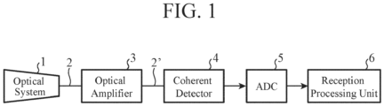
- FIG. 1 is a configuration diagram illustrating a receiver according to a first embodiment.
- the receiver illustrated in FIG. 1 includes an optical system 1, optical fibers 2 and 2', an optical amplifier 3, a coherent detector 4, an analog-to-digital converter (hereinafter referred to as "ADC") 5, and a reception processing unit 6.
- ADC analog-to-digital converter
- the optical system 1 collects light propagated through space and couples the collected light to the optical fiber 2.
- the light propagated through the space is light transmitted from a transmitter (not illustrated), and the baseband signal of the light transmitted from the transmitter is modulated by, for example, a modulation system of quadrature phase shift keying (QPSK) or 8PSK.
- QPSK quadrature phase shift keying
- 8PSK 8PSK
- the optical fiber 2 transmits the light collected by the optical system 1 to the optical amplifier 3.
- the optical amplifier 3 amplifies the light so that the power of the light transmitted by the optical fiber 2 turns into a predetermined power.
- the optical amplifier 3 outputs the amplified light to the coherent detector 4 via the optical fiber 2'.
- the optical fiber 2' connects the optical amplifier 3 and the coherent detector 4, and transmits the light output from the optical amplifier 3 to the coherent detector 4.
- the coherent detector 4 coherently detects the amplified light output from the optical amplifier 3 and outputs a detection signal of the light to the ADC 5 as a coherent detection result of the light.
- the detection signal is an electrical signal.
- the coherent detector 4 performs coherent detection by making the amplified light output from the optical amplifier 3 and light having the same frequency interfere with each other.
- the frequency of the detection signal of light that is the coherent detection result is ideally in agreement with the frequency of the baseband signal.
- the frequency of the amplified light output from the optical amplifier 3 may be slightly different from the frequency of the light to be interfered with, a deviation may occur between the frequency of the detection signal of the light and the frequency of the baseband signal.
- a frequency compensation unit 21 described later compensates the frequency of a digital detection signal output from an adaptive filter 14 described later.
- the ADC 5 converts the detection signal output from the coherent detector 4 from an analog signal to a digital signal (hereinafter, referred to as a "digital detection signal").
- the ADC 5 outputs the digital detection signal to the reception processing unit 6.
- the reception processing unit 6 compensates the digital detection signal output from the ADC 5 and demodulates the compensated digital detection signal.
- FIG. 2 is a configuration diagram illustrating the reception processing unit 6 of the receiver according to the first embodiment.
- FIG. 3 is a hardware configuration diagram illustrating hardware of the reception processing unit 6 of the receiver according to the first embodiment.
- a clock extraction unit 11 is implemented by, for example, a clock extraction circuit 31 illustrated in FIG. 3 .
- the clock extraction unit 11 extracts a clock signal superimposed on the digital detection signal output from the ADC 5.
- the clock signal can be extracted from the digital detection signal by using, for example, a technique called “clock data recovery (CDR)" described in Non-Patent Literature 1 below.
- CDR clock data recovery
- the clock extraction unit 11 outputs the extracted clock signal to a degradation determination unit 12 described later.
- the degradation determination unit 12 is implemented by, for example, a degradation determination circuit 32 illustrated in FIG. 3 .
- the degradation determination unit 12 determines whether or not the SNR (signal-to-noise ratio) of the digital detection signal output from the ADC 5 is lower than the SNR at which the digital detection signal can be demodulated (hereinafter referred to as the "demodulatable SNR").
- the degradation determination unit 12 compares the amplitude of the clock signal extracted by the clock extraction unit 11 with a threshold, and determines that the SNR of the digital detection signal is not lower than the demodulatable SNR when the amplitude of the clock signal is equal to or greater than the threshold.
- the degradation determination unit 12 determines that the SNR of the digital detection signal is lower than the demodulatable SNR.
- each of an equalization unit 13 and an equalization unit 20 described later can equalize the digital detection signal, and when the amplitude of the clock signal is less than the threshold, each of the equalization unit 13 and the equalization unit 20 may not be able to equalize the digital detection signal.
- the threshold may be stored in the internal memory of the degradation determination unit 12 or may be given from the outside of the reception processing unit 6.
- the degradation determination unit 12 outputs a determination result, indicating whether or not the SNR of the digital detection signal is lower than the demodulatable SNR, to each of a coefficient update processing unit 17 of a coefficient update unit 16 to be described later and a compensation value update processing unit 24 of a compensation value update unit 23 to be described later.
- the equalization unit 13 includes an adaptive filter 14, a coefficient calculating unit 15, and a coefficient update unit 16.
- the adaptive filter 14 is implemented by, for example, a digital filter circuit 33 illustrated in FIG. 3 .
- the adaptive filter 14 compensates a signal value of the digital detection signal output from the ADC 5 using a filter coefficient stored in a coefficient storage unit 18 described later.
- the adaptive filter 14 outputs the digital detection signal after the signal value compensation to each of the coefficient calculating unit 15, and the frequency compensation unit 21 and a compensation value calculating unit 22 of the equalization unit 20 described later.
- the coefficient calculating unit 15 is implemented by, for example, a coefficient calculating circuit 34 illustrated in FIG. 3 .
- the coefficient calculating unit 15 calculates, as a filter coefficient used by the adaptive filter 14, a filter coefficient in which a signal value of the detection signal output from the adaptive filter 14 is a reference value.
- the internal memory of the coefficient calculating unit 15 stores a reference value corresponding to the signal value of the digital detection signal output from the ADC 5.
- the coefficient calculating unit 15 acquires a reference value corresponding to the signal value of the digital detection signal output from the ADC 5 from among the reference values stored in the internal memory, and acquires the filter coefficient stored in the coefficient storage unit 18.
- the coefficient calculating unit 15 newly calculates a filter coefficient in which the signal value of the detection signal output from the adaptive filter 14 is the acquired reference value by using the filter coefficient stored in the coefficient storage unit 18.
- the filter coefficient calculation processing itself by the coefficient calculating unit 15 is a known technique, and thus detailed description thereof will be omitted. Note that, in a case where the modulation system of light is, for example, QPSK, the filter coefficient can be calculated by executing a known constant modulus algorithm (CMA).
- CMA constant modulus algorithm
- the filter coefficient calculated by the coefficient calculating unit 15 does not need to be a filter coefficient in which the signal value of the detection signal output from the adaptive filter 14 exactly matches the acquired reference value, and may be a filter coefficient in which the signal value of the detection signal output from the adaptive filter 14 is different from the acquired reference value as long as there is no practical problem.
- the coefficient calculating unit 15 outputs the calculated filter coefficient to the coefficient update processing unit 17 of the coefficient update unit 16.
- the signal value of the digital detection signal varies depending on the modulation system of light.
- the reference value is 0, 1, 2, 3, 4, and 5.
- a signal value of the digital detection signal output from the ADC 5 may deviate from the reference value due to a modulation abnormality of light in a transmitter (not illustrated), an influence of the atmosphere, or the like.
- Signal value of digital detection signal output from ADC 5 Reference value 0 to less than 0.5 ⁇ 0 0.5 to less than 1.5 ⁇ 1 1.5 to less than 2.5 ⁇ 2 2.5 to less than 3.5 ⁇ 3 3.5 to less than 4.5 ⁇ 4 4.5 or above ⁇ 5
- the coefficient update unit 16 includes the coefficient update processing unit 17, the coefficient storage unit 18, and a first first-in first-out memory (hereinafter, referred to as a "first FIFO memory") 19.
- the coefficient update unit 16 stores the filter coefficient calculated by the coefficient calculating unit 15.
- the coefficient update unit 16 changes the filter coefficient used by the adaptive filter 14 to the filter coefficient calculated by the coefficient calculating unit 15.
- the coefficient update unit 16 changes the filter coefficient used by the adaptive filter 14 to the stored filter coefficient.
- the coefficient update processing unit 17 is implemented by, for example, a coefficient update processing circuit 35 illustrated in FIG. 3 .
- the coefficient update processing unit 17 causes the coefficient storage unit 18 to store the filter coefficient calculated by the coefficient calculating unit 15, thereby changing the filter coefficient used by the adaptive filter 14 to the filter coefficient calculated by the coefficient calculating unit 15.
- the coefficient update processing unit 17 causes the first FIFO memory 19 to store the filter coefficient calculated by the coefficient calculating unit 15.
- the coefficient update processing unit 17 stops the filter coefficient calculation processing in the coefficient calculating unit 15.
- the coefficient update processing unit 17 reads the filter coefficient stored earliest among the filter coefficients stored in the first FIFO memory 19.
- the coefficient update processing unit 17 changes the filter coefficient used by the adaptive filter 14 to the readout filter coefficient by causing the coefficient storage unit 18 to store the readout filter coefficient.
- the coefficient storage unit 18 is implemented by, for example, a coefficient storage circuit 36 illustrated in FIG. 3 .
- the coefficient storage unit 18 stores filter coefficients used by the adaptive filter 14.
- the first FIFO memory 19 is implemented by, for example, a FIFO memory circuit 37 illustrated in FIG. 3 .
- the first FIFO memory 19 is a first-in first-out storage medium for storing the filter coefficients calculated by the coefficient calculating unit 15.
- the first FIFO memory 19 When the number of filter coefficients to be stored is D, and the first FIFO memory 19 receives the filter coefficient from the coefficient update processing unit 17, the first FIFO memory 19 stores the filter coefficient.
- the first FIFO memory 19 upon receiving a filter coefficient from the coefficient update processing unit 17, the first FIFO memory 19 discards the filter coefficient stored earliest when storing the filter coefficient.
- a calculation cycle T of the filter coefficient in the coefficient calculating unit 15 is shorter than a required extraction time E of a clock signal in the clock extraction unit 11, and a value obtained by multiplying the number D of filter coefficients to be stored by the calculation cycle T is equal to or longer than the required extraction time E.
- the equalization unit 20 includes a frequency compensation unit 21, a compensation value calculating unit 22, and a compensation value update unit 23.
- the frequency compensation unit 21 is implemented by, for example, a frequency compensation circuit 38 shown in FIG. 3 .
- the frequency compensation unit 21 uses a frequency compensation value stored in a compensation value storage unit 25 described later to compensate the frequency of the digital detection signal output from the adaptive filter 14 by phase-rotating the digital detection signal output from the adaptive filter 14.
- the frequency compensation unit 21 outputs the frequency-compensated digital detection signal to each of the compensation value calculating unit 22 and a phase compensation unit 27 described later.
- the compensation value calculating unit 22 is implemented by, for example, a compensation value calculating circuit 39 illustrated in FIG. 3 .
- the compensation value calculating unit 22 calculates the frequency of the digital detection signal output from the adaptive filter 14 as the frequency compensation value used for the phase rotation of the digital detection signal by the frequency compensation unit 21
- the compensation value calculating unit 22 calculates a new frequency compensation value from the digital detection signal output from the adaptive filter 14, the frequency compensated digital detection signal output from the frequency compensation unit 21, and the frequency compensation value stored in the compensation value storage unit 25 as the frequency compensation value used for phase rotation of the digital detection signal by the frequency compensation unit 21.
- Non-Patent Literature 2 discloses a calculation method of the frequency compensation value.
- the compensation value calculating unit 22 outputs the calculated frequency compensation value to the compensation value update processing unit 24 of the compensation value update unit 23.
- the compensation value update unit 23 includes the compensation value update processing unit 24, the compensation value storage unit 25, and a second first-in first-out memory (hereinafter, referred to as a "second FIFO memory") 26.
- the compensation value update unit 23 stores the frequency compensation value calculated by the compensation value calculating unit 22.
- the frequency compensation unit 21 is caused to change the frequency compensation value used for phase rotation of the digital detection signal to the frequency compensation value calculated by the compensation value calculating unit 22.
- the compensation value update unit 23 causes the frequency compensation unit 21 to change the frequency compensation value used for phase rotation of the digital detection signal to the stored frequency compensation value.
- the compensation value update processing unit 24 is implemented by, for example, a compensation value update processing circuit 40 illustrated in FIG. 3 .
- the compensation value update processing unit 24 causes the compensation value storage unit 25 to store the frequency compensation value calculated by the compensation value calculating unit 22, thereby causing the frequency compensation unit 21 to change the frequency compensation value used for phase rotation of the digital detection signal to the frequency compensation value calculated by the compensation value calculating unit 22.
- the compensation value update processing unit 24 causes the second FIFO memory 26 to store the frequency compensation value calculated by the compensation value calculating unit 22.
- the compensation value update processing unit 24 stops the frequency compensation value calculation processing in the compensation value calculating unit 22.
- the compensation value update processing unit 24 reads the frequency compensation value stored earliest among the frequency compensation values stored in the second FIFO memory 26.
- the compensation value update processing unit 24 causes the compensation value storage unit 25 to store the read frequency compensation value, thereby causing the frequency compensation unit 21 to change the frequency compensation value used for phase rotation of the digital detection signal to the read frequency compensation value.
- the compensation value storage unit 25 is implemented by, for example, a compensation value storage circuit 41 illustrated in FIG. 3 .
- the compensation value storage unit 25 stores a frequency compensation value used for phase rotation of the digital detection signal by the frequency compensation unit 21.
- the second FIFO memory 26 is implemented by, for example, a FIFO memory circuit 42 illustrated in FIG. 3 .
- the second FIFO memory 26 is a first-in first-out storage medium to store the frequency compensation value calculated by the compensation value calculating unit 22.
- the second FIFO memory 26 When the number of frequency compensation values to be stored is D' and the second FIFO memory 26 receives the frequency compensation value from the compensation value update processing unit 24, the second FIFO memory 26 stores the frequency compensation value.
- the second FIFO memory 26 upon receiving a frequency compensation value from the compensation value update processing unit 24, the second FIFO memory 26 discards the frequency compensation value stored earliest when storing the frequency compensation value.
- the calculation cycle T' of the frequency compensation value in the compensation value calculating unit 22 is shorter than the required extraction time E of the clock signal in the clock extraction unit 11, and a value obtained by multiplying the number D' of frequency compensation values to be stored by the calculation cycle T' is equal to or longer than the required extraction time E.
- the phase compensation unit 27 is implemented by, for example, a phase compensation circuit 43 shown in FIG. 3 .
- the phase compensation unit 27 compensates the phase of the frequency-compensated digital detection signal output from the frequency compensation unit 21.
- the phase compensation unit 27 outputs the phase-compensated digital detection signal to the signal determination unit 28.
- the signal determination unit 28 is implemented by, for example, a signal determination circuit 44 illustrated in FIG. 3 .
- the signal determination unit 28 demodulates the phase-compensated digital detection signal output from the phase compensation unit 27.
- the digital detection signal is demodulated by the QPSK demodulation system.
- the digital detection signal is demodulated by the demodulation system of 8PSK.
- each of the clock extraction unit 11, the degradation determination unit 12, the adaptive filter 14, the coefficient calculating unit 15, the coefficient update processing unit 17, the coefficient storage unit 18, the first FIFO memory 19, the frequency compensation unit 21, the compensation value calculating unit 22, the compensation value update processing unit 24, the compensation value storage unit 25, the second FIFO memory 26, the phase compensation unit 27, and the signal determination unit 28, which are components of the reception processing unit 6, is implemented by dedicated hardware as illustrated in FIG. 3 .
- reception processing unit 6 is implemented by the clock extraction circuit 31, the degradation determination circuit 32, the digital filter circuit 33, the coefficient calculating circuit 34, the coefficient update processing circuit 35, the coefficient storage circuit 36, the FIFO memory circuit 37, the frequency compensation circuit 38, the compensation value calculating circuit 39, the compensation value update processing circuit 40, the compensation value storage circuit 41, the FIFO memory circuit 42, the phase compensation circuit 43, and the signal determination circuit 44.
- each of the coefficient storage circuit 36, the FIFO memory circuit 37, the compensation value storage circuit 41, and the FIFO memory circuit 42 is, for example, a nonvolatile or volatile semiconductor memory, such as a RAM (Random Access Memory), a ROM (Read Only Memory), a flash memory, an EPROM (Erasable Programmable Read Only Memory), and an EEPROM (Electrically Erasable Programmable Read Only Memory), a magnetic disk, a flexible disk, an optical disk, a compact disk, a mini disk, a DVD (Digital Versatile Disc), or the like.
- a nonvolatile or volatile semiconductor memory such as a RAM (Random Access Memory), a ROM (Read Only Memory), a flash memory, an EPROM (Erasable Programmable Read Only Memory), and an EEPROM (Electrically Erasable Programmable Read Only Memory), a magnetic disk, a flexible disk, an optical disk, a compact disk, a mini disk, a DVD (Digital Versatile Disc), or the like
- each of the clock extraction circuit 31, the degradation determination circuit 32, the digital filter circuit 33, the coefficient calculating circuit 34, the coefficient update processing circuit 35, the frequency compensation circuit 38, the compensation value calculating circuit 39, the compensation value update processing circuit 40, the phase compensation circuit 43, and the signal determination circuit 44 corresponds to, for example, a single circuit, a composite circuit, a programmed processor, a parallel-programmed processor, an application specific integrated circuit (ASIC), a field-programmable gate array (FPGA), or a combination thereof.
- ASIC application specific integrated circuit
- FPGA field-programmable gate array
- reception processing unit 6 The components of the reception processing unit 6 are not limited to those implemented by dedicated hardware, but the reception processing unit 6 may be implemented by software, firmware, or a combination of software and firmware.
- the software or firmware is stored in a memory of a computer as a program.
- the computer means hardware that executes a program, and corresponds to, for example, a central processing unit (CPU), a central processing unit, a processing unit, an arithmetic unit, a microprocessor, a microcomputer, a processor, or a digital signal processor (DSP).
- CPU central processing unit
- CPU central processing unit
- processing unit processing unit
- an arithmetic unit a microprocessor
- microcomputer a processor
- DSP digital signal processor
- FIG. 4 is a hardware configuration diagram of a computer when the reception processing unit 6 is implemented by software, firmware, or the like.
- the coefficient storage unit 18, the first FIFO memory 19, the compensation value storage unit 25, and the second FIFO memory 26 are configured on a memory 51 of the computer.
- a program for causing a computer to execute processing procedures performed by the clock extraction unit 11, the degradation determination unit 12, the adaptive filter 14, the coefficient calculating unit 15, the coefficient update processing unit 17, the frequency compensation unit 21, the compensation value calculating unit 22, the compensation value update processing unit 24, the phase compensation unit 27, and the signal determination unit 28 is stored in the memory 51.
- a processor 52 of the computer executes the program stored in the memory 51.
- FIG. 3 illustrates an example in which each of the components of the reception processing unit 6 is implemented by dedicated hardware
- FIG. 4 illustrates an example in which the reception processing unit 6 is implemented by software, firmware, or the like.
- this is merely an example, and some components in the reception processing unit 6 may be implemented by dedicated hardware, and the remaining components may be implemented by software, firmware, or the like.
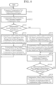
- FIG. 5 is a flowchart illustrating a processing procedure performed by the equalization unit 13 in the reception processing unit 6.
- FIG. 6 is a flowchart illustrating a processing procedure performed by the equalization unit 20 in the reception processing unit 6.
- a transmitter modulates light emitted from a light source (not illustrated) depending on information on a communication target.
- a modulation system of light for example, a modulation system of QPSK or 8PSK can be used.
- the transmitter (not illustrated) emits light modulated depending on information on a communication target to space.
- the optical system 1 collects light emitted from a transmitter (not illustrated) and then propagated through the space, and couples the collected light to the optical fiber 2.
- the optical fiber 2 transmits the light collected by the optical system 1 to the optical amplifier 3.
- the optical amplifier 3 amplifies the light so that the power of the light transmitted by the optical fiber 2 turns into a predetermined power.
- the optical amplifier 3 outputs the amplified light to the coherent detector 4 via the optical fiber 2'.
- the coherent detector 4 Upon receiving the amplified light from the optical amplifier 3, the coherent detector 4 coherently detects the amplified light.
- the coherent detector 4 outputs a detection signal of light to the ADC 5 as a coherent detection result of light.
- the ADC 5 Upon receiving the detection signal from the coherent detector 4, the ADC 5 converts the detection signal from an analog signal to a digital signal.
- the ADC 5 outputs the digital detection signal, which is a digital signal, to each of the clock extraction unit 11, the adaptive filter 14, and the coefficient calculating unit 15 of the reception processing unit 6.
- the reception processing unit 6 Upon receiving the digital detection signal from the ADC 5, the reception processing unit 6 compensates the digital detection signal and demodulates the compensated digital detection signal.
- the clock extraction unit 11 Upon receiving the digital detection signal from the ADC 5, the clock extraction unit 11 extracts the clock signal superimposed on the digital detection signal by using, for example, a technology called CDR.
- the clock extraction unit 11 outputs the extracted clock signal to the degradation determination unit 12.
- the degradation determination unit 12 determines whether or not the SNR of the digital detection signal output from the ADC 5 is lower than the demodulatable SNR on the basis of the amplitude of the clock signal.
- the degradation determination unit 12 compares the amplitude of the clock signal extracted by the clock extraction unit 11 with a threshold, and determines that the SNR of the digital detection signal is not lower than the demodulatable SNR when the amplitude of the clock signal is equal to or greater than the threshold.
- the degradation determination unit 12 determines that the SNR of the digital detection signal is lower than the demodulatable SNR.
- the degradation determination unit 12 outputs a determination result, indicating whether or not the SNR of the digital detection signal is lower than the demodulatable SNR, to each of the coefficient update processing unit 17 and the compensation value update processing unit 24.
- the adaptive filter 14 Upon receiving the digital detection signal from the ADC 5, the adaptive filter 14 compensates the signal value of the digital detection signal by using the filter coefficient stored by the coefficient storage unit 18 (step ST1 in FIG. 5 ).
- the adaptive filter 14 outputs the digital detection signal after the signal value compensation to each of the coefficient calculating unit 15, the frequency compensation unit 21, and the compensation value calculating unit 22.
- the adaptive filter 14 compensates the signal value of the digital detection signal, so that the signal value of the digital detection signal can be brought close to the reference value, for example, even if the time variation in the phase of the clock signal superimposed on the digital detection signal or the time variation in the frequency characteristic of the digital detection signal occurs.
- the filter coefficient stored in the coefficient storage unit 18 is an appropriate coefficient
- the signal value of the digital detection signal output from the adaptive filter 14 substantially matches the reference value
- the signal value of the digital detection signal is modulated to be any value of 0, 1, 2, 3, 4, and 5, for example, and the filter coefficient stored by the coefficient storage unit 18 is an appropriate coefficient.
- the signal value of the digital detection signal output from the ADC 5 is, for example, "2.8"
- the signal value of the digital detection signal output from the adaptive filter 14 is approximately "3".
- the signal value of the digital detection signal output from the ADC 5 is, for example, "4.3"
- the signal value of the digital detection signal output from the adaptive filter 14 is approximately "4".
- the coefficient calculating unit 15 Upon receiving the digital detection signal from the ADC 5, the coefficient calculating unit 15 acquires a reference value corresponding to the signal value of the digital detection signal from among the reference values stored in the internal memory. In a case where the signal value of the digital detection signal is modulated to any value of, for example, 0, 1, 2, 3, 4, and 5, the coefficient calculating unit 15 acquires "3" as a reference value when the signal value of the digital detection signal is, for example, "2.7”, and acquires "1" as a reference value when the signal value of the digital detection signal is, for example, "1.3".
- the coefficient calculating unit 15 acquires the filter coefficient stored by the coefficient storage unit 18.
- the coefficient calculating unit 15 newly calculates the filter coefficient in which the signal value of the detection signal output from the adaptive filter 14 is the acquired reference value by using the filter coefficient stored by the coefficient storage unit 18 (step ST2 in FIG. 5 ).
- the coefficient calculating unit 15 outputs the calculated filter coefficient to the coefficient update processing unit 17.
- the calculation cycle T of the filter coefficient in the coefficient calculating unit 15 is shorter than the required extraction time E of the clock signal in the clock extraction unit 11.
- the coefficient calculating unit 15 calculates the filter coefficient N times while the clock extraction unit 11 extracts the clock signal once.
- N is an integer equal to or more than two.
- the coefficient update processing unit 17 acquires the determination result output from the degradation determination unit 12.
- the coefficient update processing unit 17 causes the coefficient storage unit 18 to store the filter coefficient calculated by the coefficient calculating unit 15 (step ST4 in FIG. 5 ).
- the coefficient update processing unit 17 causes the coefficient storage unit 18 to store the filter coefficient calculated by the coefficient calculating unit 15, so that the filter coefficient used by the adaptive filter 14 for signal value compensation is changed to the filter coefficient calculated by the coefficient calculating unit 15.
- the coefficient update processing unit 17 causes the first FIFO memory 19 to store the filter coefficient calculated by the coefficient calculating unit 15 (step ST5 in FIG. 5 ).
- the first FIFO memory 19 stores the filter coefficient output from the coefficient update processing unit 17. However, when the first FIFO memory 19 has already stored the D filter coefficients, upon receiving a filter coefficient from the coefficient update processing unit 17, the first FIFO memory 19 discards the filter coefficient stored earliest when storing the filter coefficient.
- the adaptive filter 14 Upon receiving a new digital detection signal from the ADC 5, the adaptive filter 14 compensates the signal value of the digital detection signal by using the filter coefficient stored in the coefficient storage unit 18 (step ST1 in FIG. 5 ).
- the adaptive filter 14 outputs the digital detection signal after the signal value compensation to each of the coefficient calculating unit 15, the frequency compensation unit 21, and the compensation value calculating unit 22.
- the coefficient update processing unit 17 stops the calculation processing of filter coefficient in the coefficient calculating unit 15 (step ST6 in FIG. 5 ).
- the coefficient update processing unit 17 reads the filter coefficient stored earliest among the filter coefficients stored in the first FIFO memory 19.
- the coefficient update processing unit 17 causes the coefficient storage unit 18 to store the readout filter coefficient (step ST7 in FIG. 5 ).
- the coefficient update processing unit 17 causes the coefficient storage unit 18 to store the readout filter coefficient, so that the filter coefficient used by the adaptive filter 14 for signal value compensation is changed to the readout filter coefficient.
- the calculation cycle T of the filter coefficient in the coefficient calculating unit 15 is shorter than the required extraction time E of the clock signal in the clock extraction unit 11, and a value obtained by multiplying the number D of filter coefficients to be stored by the calculation cycle T is equal to or longer than the required extraction time E.
- the readout filter coefficient is the filter coefficient calculated by the coefficient calculating unit 15 at a time D ⁇ T before the current time. Note that the readout filter coefficient is a filter coefficient calculated by the coefficient calculating unit 15 when the SNR of the digital detection signal is not lower than the demodulatable SNR.
- the adaptive filter 14 Upon receiving a new digital detection signal from the ADC 5, the adaptive filter 14 compensates the signal value of the digital detection signal by using the filter coefficient stored in the coefficient storage unit 18 (step ST8 in FIG. 5 ).
- the adaptive filter 14 outputs the digital detection signal after the signal value compensation to each of the coefficient calculating unit 15, the frequency compensation unit 21, and the compensation value calculating unit 22.
- the coefficient update processing unit 17 restarts the calculation processing of filter coefficient in the coefficient calculating unit 15 (step ST10 in FIG. 5 ).
- the adaptive filter 14 compensates the signal value of the digital detection signal by using the filter coefficient stored in the coefficient storage unit 18 (step ST8 in FIG. 5 ).
- the equalization unit 13 repeatedly performs the processing of steps ST1 to ST 10 in FIG. 5 .
- the frequency compensation unit 21 Upon receiving the digital detection signal from the adaptive filter 14, the frequency compensation unit 21 uses the frequency compensation value stored in the compensation value storage unit 25 to compensate the frequency of the digital detection signal by phase-rotating the digital detection signal (step ST11 in FIG. 6 ).
- the frequency compensation unit 21 outputs the detection signal after the frequency compensation to each of the compensation value calculating unit 22 and the phase compensation unit 27.
- the frequency compensation unit 21 compensates the frequency of the digital detection signal, for example, even if the frequency of the amplified light output from the optical amplifier 3 and the frequency of the light to be interfered are slightly different, it is possible to eliminate the deviation between the frequency of the digital detection signal and the frequency of the baseband signal.
- the compensation value calculating unit 22 calculates a new frequency compensation value from the digital detection signal output from the adaptive filter 14, the frequency compensated digital detection signal output from the frequency compensation unit 21, and the frequency compensation value stored in the compensation value storage unit 25, as the frequency compensation value used for phase rotation of the digital detection signal by the frequency compensation unit 21 (step ST12 in FIG. 6 ).
- the compensation value calculating unit 22 outputs the calculated frequency compensation value to the compensation value update processing unit 24 of the compensation value update unit 23.
- the calculation cycle T' of the frequency compensation value in the compensation value calculating unit 22 is shorter than the required extraction time E of the clock signal in the clock extraction unit 11.
- the compensation value calculating unit 22 calculates the filter coefficient N' times while the clock extraction unit 11 extracts the clock signal once.
- N' is an integer equal to or more than two.
- the compensation value update processing unit 24 acquires the determination result output from the degradation determination unit 12.
- the compensation value update processing unit 24 causes the compensation value storage unit 25 to store the frequency compensation value calculated by the compensation value calculating unit 22 (step ST14 in FIG. 6 ).
- the compensation value update processing unit 24 causes the compensation value storage unit 25 to store the frequency compensation value calculated by the compensation value calculating unit 22, whereby the frequency compensation unit 21 changes the frequency compensation value used for phase rotation of the digital detection signal to the frequency compensation value calculated by the compensation value calculating unit 22.
- the compensation value update processing unit 24 causes the second FIFO memory 26 to store the frequency compensation value calculated by the compensation value calculating unit 22 (step ST15 in FIG. 6 ).
- the second FIFO memory 26 stores the frequency compensation value output from the compensation value update processing unit 24. However, when the second FIFO memory 26 has already stored D' frequency compensation values, upon receiving a frequency compensation value from the compensation value update processing unit 24, the second FIFO memory 26 discards the frequency compensation value stored earliest when storing the frequency compensation value.
- the frequency compensation unit 21 Upon receiving a new digital detection signal from the adaptive filter 14, the frequency compensation unit 21 uses the frequency compensation value stored in the compensation value storage unit 25 to compensate the frequency of the digital detection signal by phase-rotating the digital detection signal (step ST11 in FIG. 6 ).
- the frequency compensation unit 21 outputs the detection signal after the frequency compensation to each of the compensation value calculating unit 22 and the phase compensation unit 27.
- step ST13 in FIG. 6 NO
- the compensation value update processing unit 24 stops the frequency compensation value calculation processing in the compensation value calculating unit 22 (step ST16 in FIG. 6 ).
- the compensation value update processing unit 24 reads the frequency compensation value stored earliest among the frequency compensation values stored in the second FIFO memory 26.
- the compensation value update processing unit 24 causes the compensation value storage unit 25 to store the read frequency compensation value (step ST17 in FIG. 6 ).
- the compensation value update processing unit 24 causes the compensation value storage unit 25 to store the read frequency compensation value, whereby the frequency compensation unit 21 changes the frequency compensation value used for phase rotation of the digital detection signal to the read frequency compensation value.
- the calculation cycle T' of the frequency compensation value in the compensation value calculating unit 22 is shorter than the required extraction time E of the clock signal in the clock extraction unit 11, and a value obtained by multiplying the number D' of the frequency compensation values to be stored by the calculation cycle T' is equal to or longer than the required extraction time E.
- the second FIFO memory 26 stores, for example, D' frequency compensation values
- the read frequency compensation value is a frequency compensation value calculated by the compensation value calculating unit 22 at a time D' ⁇ T' before the current time.
- the read frequency compensation value is a frequency compensation value calculated by the compensation value calculating unit 22 when the SNR of the digital detection signal is not lower than the demodulatable SNR.
- the frequency compensation unit 21 Upon receiving a new digital detection signal from the adaptive filter 14, the frequency compensation unit 21 uses the frequency compensation value stored in the compensation value storage unit 25 to compensate the frequency of the digital detection signal by phase-rotating the digital detection signal (step ST18 in FIG. 6 ).
- the frequency compensation unit 21 outputs the detection signal after the frequency compensation to each of the compensation value calculating unit 22 and the phase compensation unit 27.
- the compensation value update processing unit 24 restarts the frequency compensation value calculation processing in the compensation value calculating unit 22 (step ST20 in FIG. 6 ).
- the frequency compensation unit 21 uses the frequency compensation value stored in the compensation value storage unit 25 to compensate the frequency of the digital detection signal by phase-rotating the digital detection signal output from the adaptive filter 14 (step ST18 in FIG. 6 ).
- the equalization unit 20 repeatedly performs the processing of steps ST 11 to ST 20 in FIG. 6 .
- phase compensation unit 27 compensates the phase of the digital detection signal.
- phase compensation processing itself of the digital detection signal by the phase compensation unit 27 is a known technique, detailed description thereof will be omitted.
- the phase compensation unit 27 outputs the phase-compensated digital detection signal to the signal determination unit 28.
- the signal determination unit 28 demodulates the phase-compensated digital detection signal.
- the signal determination unit 28 outputs the demodulation result of the digital detection signal to the outside.
- the receiver is configured to include the clock extraction unit 11 to extract the clock signal superimposed on the detection signal of the light propagated through the space, the degradation determination unit 12 to determine whether or not the SNR of the detection signal is lower than the SNR at which the detection signal can be demodulated on the basis of the amplitude of the clock signal extracted by the clock extraction unit 11, the adaptive filter 14 to compensate the signal value of the detection signal using the filter coefficient and output the detection signal after the signal value compensation, and the coefficient calculating unit 15 to calculate, as the filter coefficient, the filter coefficient in which the signal value of the detection signal output from the adaptive filter 14 is the reference value, in which the coefficient update unit 16 stores the filter coefficient calculated by the coefficient calculating unit 15 when the degradation determination unit 12 determines that there is no SNR degradation, and changes the filter coefficient used by the adaptive filter 14 to the stored filter coefficient when the degradation determination unit 12 determines that SNR degradation occurs.
- the receiver can improve the bit error rate without newly calculating the filter coefficient used by the adaptive filter 14 and performing the process of updating the filter coefficient used by the adaptive filter 14.
- the receiver is configured to include the frequency compensation unit 21 to compensate the frequency of the detection signal output from the adaptive filter 14 by phase-rotating the detection signal output from the adaptive filter 14 using the frequency compensation value, and outputs the detection signal after the frequency compensation, and the compensation value calculating unit 22 to calculate the frequency of the detection signal output from the adaptive filter 14 as the frequency compensation value, in which the compensation value update unit 23 stores the frequency compensation value calculated by the compensation value calculating unit 22 when the degradation determination unit 12 determines that there is no SNR degradation, and causes the frequency compensation unit 21 to change the frequency compensation value used for the phase rotation of the detection signal to the stored frequency compensation value when the degradation determination unit 12 determines that SNR degradation occurs.
- the receiver can improve the bit error rate without newly calculating the frequency compensation value used for the phase rotation of the detection signal output from the adaptive filter 14 and performing the process of updating the frequency compensation value used for the phase rotation of the digital detection signal by the frequency compensation unit 21.
- the receiver illustrated in FIG. 2 includes both the equalization unit 13 and the equalization unit 20. However, this is merely an example, and the receiver may include any one of the equalization unit 13 and the equalization unit 20.
- a receiver including an abnormality determination unit 61 to determine a type of abnormality in optical communication will be described.
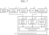
- FIG. 7 is a configuration diagram illustrating a receiver according to the second embodiment.
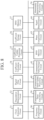
- FIG. 8 is a hardware configuration diagram illustrating part of hardware of the reception processing unit 6 and hardware of the abnormality determination unit 61 in the receiver according to the second embodiment.
- FIGS. 7 and 8 the same reference numerals as those in FIGS. 1 and 3 denote the same or corresponding parts, and thus detailed description thereof is omitted.
- the abnormality determination unit 61 includes an optical power detector 62, a signal power detector 63, an amplitude detector 64, and an abnormality determination processing unit 65.
- the abnormality determination unit 61 determines a type of abnormality in optical communication from the power of light propagated through the space, the power of the digital detection signal output from the ADC 5, and the amplitude of the clock signal extracted by the clock extraction unit 11 of the reception processing unit 6.
- the optical power detector 62 detects the power of light propagated through the space and then collected by the optical system 1, and outputs a first digital signal indicating the power of the light to the abnormality determination processing unit 65.
- the signal power detector 63 detects the power of the digital detection signal output from the ADC 5, and outputs a second digital signal indicating the power of the digital detection signal to the abnormality determination processing unit 65.
- the amplitude detector 64 detects the amplitude of the clock signal extracted by the clock extraction unit 11, and outputs a third digital signal indicating the amplitude of the clock signal to the abnormality determination processing unit 65.
- the abnormality determination processing unit 65 is implemented by, for example, an abnormality determination processing circuit 70 illustrated in FIG. 8 .
- the abnormality determination processing unit 65 determines a type of abnormality in optical communication from the first digital signal output from the optical power detector 62, the second digital signal output from the signal power detector 63, and the third digital signal output from the amplitude detector 64.
- reception processing unit 6 is implemented by the clock extraction circuit 31, the degradation determination circuit 32, the digital filter circuit 33, the coefficient calculating circuit 34, the coefficient update processing circuit 35, the coefficient storage circuit 36, the FIFO memory circuit 37, the frequency compensation circuit 38, the compensation value calculating circuit 39, the compensation value update processing circuit 40, the compensation value storage circuit 41, the FIFO memory circuit 42, the phase compensation circuit 43, and the signal determination circuit 44, and a part of the abnormality determination unit 61 is implemented by the abnormality determination processing circuit 70.
- the abnormality determination processing circuit 70 corresponds to, for example, a single circuit, a composite circuit, a programmed processor, a parallel programmed processor, ASIC, FPGA, or a combination thereof.
- the components of the reception processing unit 6 and a part of the abnormality determination unit 61 are not limited to those implemented by dedicated hardware, but the reception processing unit 6 and a part of the abnormality determination unit 61 may be implemented by software, firmware, or a combination of software and firmware.
- the coefficient storage unit 18, the first FIFO memory 19, the compensation value storage unit 25, and the second FIFO memory 26 are configured on the memory 51 of the computer illustrated in FIG. 4 .
- a program for causing a computer to execute processing procedures performed by the clock extraction unit 11, the degradation determination unit 12, the adaptive filter 14, the coefficient calculating unit 15, the coefficient update processing unit 17, the frequency compensation unit 21, the compensation value calculating unit 22, the compensation value update processing unit 24, the phase compensation unit 27, the signal determination unit 28, and the abnormality determination processing unit 65 is stored in the memory 51 illustrated in FIG. 4 .
- the processor 52 illustrated in FIG. 4 executes the program stored in the memory 51.
- the receiver is similar to the receiver illustrated in FIG. 1 except for the abnormality determination unit 61, only the operation of the abnormality determination unit 61 will be described here.
- FIG. 9 is an explanatory diagram illustrating an example of a determination result of the abnormality determination unit 61.
- the optical power detector 62 of the abnormality determination unit 61 monitors the light collected by the optical system 1 and detects the power of the light.
- the optical power detector 62 outputs a first digital signal indicating the detected power of the light to the abnormality determination processing unit 65.
- the signal power detector 63 monitors the digital detection signal output from the ADC 5 and detects the power of the digital detection signal.
- the signal power detector 63 outputs a second digital signal indicating the detected power of the digital detection signal to the abnormality determination processing unit 65.
- the amplitude detector 64 monitors the clock signal extracted by the clock extraction unit 11 and detects the amplitude of the clock signal.
- the amplitude detector 64 outputs a third digital signal indicating the detected amplitude of the clock signal to the abnormality determination processing unit 65.
- the abnormality determination processing unit 65 acquires the first digital signal output from the optical power detector 62, the second digital signal output from the signal power detector 63, and the third digital signal output from the amplitude detector 64.
- the internal memory of the abnormality determination processing unit 65 stores a first threshold related to the first digital signal, a second threshold related to the second digital signal, and a third threshold related to the third digital signal.
- the internal memory of the abnormality determination processing unit 65 stores the first threshold, the second threshold, and the third threshold.
- the first threshold, the second threshold, and the third threshold may be given from the outside of the receiver.
- the abnormality determination processing unit 65 compares the first digital signal with the first threshold, and determines that the power of the light collected by the optical system 1 is high when the first digital signal is equal to or more than the first threshold.
- the abnormality determination processing unit 65 determines that the power of the light collected by the optical system 1 is low.
- the abnormality determination processing unit 65 compares the second digital signal with the second threshold, and determines that the power of the digital detection signal is high when the second digital signal is equal to or more than the second threshold.
- the abnormality determination processing unit 65 determines that the power of the digital detection signal is low.
- the abnormality determination processing unit 65 compares the third digital signal with the third threshold, and determines that the amplitude of the clock signal is high when the third digital signal is equal to or more than the third threshold.
- the abnormality determination processing unit 65 determines that the amplitude of the clock signal is low.
- the abnormality determination processing unit 65 determines that the optical communication is normally performed as illustrated in FIG. 9 when the power of the light is high, the power of the digital detection signal is high, and the amplitude of the clock signal is high.
- the abnormality determination processing unit 65 determines that a modulation abnormality of the light in the transmitter (not illustrated) occurs as illustrated in FIG. 9 . It is conceivable that since the modulation abnormality of the light occurs, the clock extraction unit 11 cannot sufficiently extract the clock signal, and the amplitude of the clock signal is low.
- the abnormality determination processing unit 65 determines that the abnormality of the wavelength deviation in which the wavelength of the light collected by the optical system 1 deviates from the wavelength of the light oscillated by the light source of the transmitter (not illustrated) occurs. It is conceivable that since the abnormality of the wavelength deviation occurs, the coherent detector 4 cannot perform the coherent detection of the light output from the optical amplifier 3 normally, and each of the power of the digital detection signal and the amplitude of the clock signal is low.
- the abnormality determination processing unit 65 determines that the power of the light collected by the optical system 1 is low due to the influence of the atmosphere, for example, as illustrated in FIG. 9 .
- the abnormality determination processing unit 65 outputs a determination result of the type of abnormality in optical communication to the outside.
- the receiver illustrated in FIG. 7 is configured to include the abnormality determination unit 61 to determine the type of abnormality in optical communication from the power of the light propagated through the space, the power of the detection signal of the light, and the amplitude of the clock signal extracted by the clock extraction unit 11. Therefore, similarly to the receiver illustrated in FIG. 1 , the receiver illustrated in FIG. 7 can improve the bit error rate and notify the determination result of the type of abnormality in optical communication.
- the present invention is suitable for a receiver that compensates for a detection signal of light propagated through space.
Landscapes
- Physics & Mathematics (AREA)
- Electromagnetism (AREA)
- Engineering & Computer Science (AREA)
- Computer Networks & Wireless Communication (AREA)
- Signal Processing (AREA)
- Optical Communication System (AREA)
Claims (14)
- Empfänger, umfassend:eine Taktextraktionseinheit (11) zum Extrahieren eines Taktsignals, das einem Erfassungssignal von sich im Raum ausbreitendem Licht überlagert ist;eine Verschlechterungsbestimmungseinheit (12) zum Bestimmen, ob ein Signal-Rausch-Verhältnis des Erfassungssignals niedriger als ein Signal-Rausch-Verhältnis ist oder nicht, bei dem das Erfassungssignal auf Grundlage einer Amplitude des Taktsignals, das durch die Taktextraktionseinheit (11) extrahiert wurde, demoduliert wird;einen adaptiven Filter (14) zum Kompensieren eines Signalwertes des Erfassungssignals unter Verwendung eines Filterkoeffizienten und zum Ausgeben eines Erfassungssignals nach der Signalwertkompensation;eine Koeffizientenberechnungseinheit (15) zum Berechnen eines Filterkoeffizienten als den Filterkoeffizienten, bei dem ein Signalwert des von dem adaptiven Filter (14) ausgegebenen Erfassungssignals ein Referenzwert ist; undeine Koeffizientenaktualisierungseinheit (16) zum Speichern des von der Koeffizientenberechnungseinheit (15) berechneten Filterkoeffizienten, wenn die Verschlechterungsbestimmungseinheit (12) bestimmt, dass keine Verschlechterung des Signal-Rausch-Verhältnisses vorliegt, und zum Ändern des von dem adaptiven Filter (14) verwendeten Filterkoeffizienten in einen gespeicherten Filterkoeffizienten, wenn die Verschlechterungsbestimmungseinheit (12) bestimmt, dass eine Verschlechterung des Signal-Rausch-Verhältnisses auftritt.
- Empfänger nach Anspruch 1, wobei die Koeffizientenaktualisierungseinheit (16) den von dem adaptiven Filter (14) verwendeten Filterkoeffizienten auf den von der Koeffizientenberechnungseinheit (15) berechneten Filterkoeffizienten ändert, wenn die Verschlechterungsbestimmungseinheit (12) bestimmt, dass keine Verschlechterung des Signal-Rausch-Verhältnisses vorliegt.
- Empfänger nach Anspruch 1, ferner umfassend:eine Frequenzkompensationseinheit (21) zum Kompensieren einer Frequenz eines von dem adaptiven Filter (14) ausgegebenen Erfassungssignals durch Phasendrehung des von dem adaptiven Filter (14) ausgegebenen Erfassungssignals unter Verwendung eines Frequenzkompensationswerts und zum Ausgeben eines Erfassungssignals nach der Frequenzkompensation;eine Kompensationswertberechnungseinheit (22) zum Berechnen einer Frequenz des von dem adaptiven Filter (14) ausgegebenen Erfassungssignals als Frequenzkompensationswert; undeine Kompensationswertaktualisierungseinheit (23) zum Speichern des von der Kompensationswertberechnungseinheit (22) berechneten Frequenzkompensationswertes, wenn die Verschlechterungsbestimmungseinheit (12) bestimmt, dass keine Verschlechterung des Signal-Rausch-Verhältnisses vorliegt, und zum Veranlassen der Frequenzkompensationseinheit (21), den für die Phasendrehung des Erfassungssignals verwendeten Frequenzkompensationswert auf einen gespeicherten Frequenzkompensationswert zu ändern, wenn die Verschlechterungsbestimmungseinheit (12) bestimmt, dass eine Verschlechterung des Signal-Rausch-Verhältnisses auftritt.
- Empfänger nach Anspruch 3, wobei die Kompensationswertaktualisierungseinheit (23) die Frequenzkompensationseinheit (21) veranlasst, den für die Phasendrehung des Erfassungssignals verwendeten Frequenzkompensationswert auf den von der Kompensationswertberechnungseinheit (22) berechneten Frequenzkompensationswert zu ändern, wenn die Verschlechterungsbestimmungseinheit (12) bestimmt, dass keine Verschlechterung des Signal-Rausch-Verhältnisses vorliegt.
- Empfänger nach Anspruch 1 oder 2, wobeiein Berechnungszyklus des Filterkoeffizienten in der Koeffizientenberechnungseinheit (15) kürzer ist als eine erforderliche Extraktionszeit des Taktsignals in der Taktextraktionseinheit (11), unddie Koeffizientenaktualisierungseinheit (16) als Speichermedium zum Speichern des von der Koeffizientenberechnungseinheit (15) berechneten Filterkoeffizienten einen ersten First-in-First-out-Speicher (19) aufweist, der eine Anzahl von Filterkoeffizienten speichern kann,wobei ein Wert, der durch Multiplizieren der Anzahl der zu speichernden Filterkoeffizienten mit dem Berechnungszyklus erhalten wird, gleich wie oder länger als die erforderliche Extraktionszeit ist.
- Empfänger nach Anspruch 3 oder 4, wobeiein Berechnungszyklus des Frequenzkompensationswertes in der Kompensationswertberechnungseinheit (22) kürzer ist als eine erforderliche Extraktionszeit des Taktsignals in der Taktextraktionseinheit (11), unddie Kompensationswertaktualisierungseinheit (23) als Speichermedium zum Speichern des von der Kompensationswertberechnungseinheit (22) berechneten Frequenzkompensationswertes einen zweiten First-in-First-out-Speicher (26) aufweist, der eine Anzahl von Frequenzkompensationswerten speichern kann,wobei ein Wert, der durch Multiplizieren der Anzahl der zu speichernden Frequenzkompensationswerte mit dem Berechnungszyklus erhalten wird, gleich wie oder länger als die erforderliche Extraktionszeit ist.
- Empfänger nach Anspruch 1, ferner umfassend eine Anomalie-Bestimmungseinheit (61) zum Bestimmen eines Typs von Anomalie in der optischen Kommunikation aus Energie von sich durch den Raum ausbreitendem Licht, Energie eines Erfassungssignals des Lichts und einer Amplitude des von der Taktextraktionseinheit (11) extrahierten Taktsignals.
- Empfänger, umfassend:eine Taktextraktionseinheit (11) zum Extrahieren eines Taktsignals, das einem Erfassungssignal von sich im Raum ausbreitendem Licht überlagert ist;eine Verschlechterungsbestimmungseinheit (12) zum Bestimmen, ob ein Signal-Rausch-Verhältnis des Erfassungssignals niedriger als ein Signal-Rausch-Verhältnis ist oder nicht, bei dem das Erfassungssignal auf Grundlage einer Amplitude des Taktsignals, das durch die Taktextraktionseinheit (11) extrahiert wurde, demoduliert wird;eine Frequenzkompensationseinheit (21) zum Kompensieren einer Frequenz des Erfassungssignals durch Phasendrehung des Erfassungssignals unter Verwendung eines Frequenzkompensationswerts und zum Ausgeben eines Erfassungssignals nach der Frequenzkompensation;eine Kompensationswertberechnungseinheit (22) zum Berechnen einer Frequenz des Erfassungssignals als Frequenzkompensationswert; undeine Kompensationswertaktualisierungseinheit (23) zum Speichern des von der Kompensationswertberechnungseinheit (22) berechneten Frequenzkompensationswertes, wenn die Verschlechterungsbestimmungseinheit (12) bestimmt, dass keine Verschlechterung des Signal-Rausch-Verhältnisses vorliegt, und zum Veranlassen der Frequenzkompensationseinheit (21), den für die Phasendrehung des Erfassungssignals verwendeten Frequenzkompensationswert auf einen gespeicherten Frequenzkompensationswert zu ändern, wenn die Verschlechterungsbestimmungseinheit (12) bestimmt, dass eine Verschlechterung des Signal-Rausch-Verhältnisses auftritt.
- Empfänger nach Anspruch 8, wobei die Kompensationswertaktualisierungseinheit (23) die Frequenzkompensationseinheit (21) veranlasst, den für die Phasendrehung des Erfassungssignals verwendeten Frequenzkompensationswert auf den von der Kompensationswertberechnungseinheit (22) berechneten Frequenzkompensationswert zu ändern, wenn die Verschlechterungsbestimmungseinheit (12) bestimmt, dass keine Verschlechterung des Signal-Rausch-Verhältnisses vorliegt.
- Empfänger nach Anspruch 8, ferner umfassend:einen adaptiven Filter (14) zum Kompensieren eines Signalwertes des Erfassungssignals von sich durch den Raum ausbreitendem Licht unter Verwendung eines Filterkoeffizienten und zum Ausgeben eines Erfassungssignals nach der Signalwertkompensation an jede der Frequenzkompensationseinheit (21) und der Kompensationswertberechnungseinheit (22);eine Koeffizientenberechnungseinheit (15) zum Berechnen eines Filterkoeffizienten als den Filterkoeffizienten, bei dem ein Signalwert des von dem adaptiven Filter (14) ausgegebenen Erfassungssignals ein Referenzwert ist; undeine Koeffizientenaktualisierungseinheit (16) zum Speichern des von der Koeffizientenberechnungseinheit (15) berechneten Filterkoeffizienten, wenn die Verschlechterungsbestimmungseinheit (12) bestimmt, dass keine Verschlechterung des Signal-Rausch-Verhältnisses vorliegt, und zum Ändern des von dem adaptiven Filter (14) verwendeten Filterkoeffizienten in einen gespeicherten Filterkoeffizienten, wenn die Verschlechterungsbestimmungseinheit (12) bestimmt, dass eine Verschlechterung des Signal-Rausch-Verhältnisses auftritt.
- Empfänger nach Anspruch 10, wobei die Koeffizientenaktualisierungseinheit (16) den von dem adaptiven Filter (14) verwendeten Filterkoeffizienten auf den von der Koeffizientenberechnungseinheit (15) berechneten Filterkoeffizienten ändert, wenn die Verschlechterungsbestimmungseinheit (12) bestimmt, dass keine Verschlechterung des Signal-Rausch-Verhältnisses vorliegt.
- Empfänger nach Anspruch 10 oder 11, wobeiein Berechnungszyklus des Filterkoeffizienten in der Koeffizientenberechnungseinheit (15) kürzer ist als eine erforderliche Extraktionszeit des Taktsignals in der Taktextraktionseinheit (11), unddie Koeffizientenaktualisierungseinheit (16) als Speichermedium zum Speichern des von der Koeffizientenberechnungseinheit (15) berechneten Filterkoeffizienten einen ersten First-in-First-out-Speicher (19) aufweist, der eine Anzahl von Filterkoeffizienten speichern kann,wobei ein Wert, der durch Multiplizieren der Anzahl der zu speichernden Filterkoeffizienten mit dem Berechnungszyklus erhalten wird, gleich wie oder länger als die erforderliche Extraktionszeit ist.
- Empfänger nach Anspruch 8 oder 9, wobeiein Berechnungszyklus des Frequenzkompensationswertes in der Kompensationswertberechnungseinheit (22) kürzer ist als eine erforderliche Extraktionszeit des Taktsignals in der Taktextraktionseinheit (11), unddie Kompensationswertaktualisierungseinheit (23) als Speichermedium zum Speichern des von der Kompensationswertberechnungseinheit (22) berechneten Frequenzkompensationswertes einen zweiten First-in-First-out-Speicher (26) aufweist, der eine Anzahl von Frequenzkompensationswerten speichern kann,wobei ein Wert, der durch Multiplizieren der Anzahl der zu speichernden Frequenzkompensationswerte mit dem Berechnungszyklus erhalten wird, gleich wie oder länger als die erforderliche Extraktionszeit ist.
- Empfänger nach Anspruch 8, ferner umfassend eine Anomalie-Bestimmungseinheit (61) zum Bestimmen eines Typs von Anomalie in der optischen Kommunikation aus Energie von sich durch den Raum ausbreitendem Licht, Energie eines Erfassungssignals des Lichts und einer Amplitude des von der Taktextraktionseinheit (11) extrahierten Taktsignals.
Applications Claiming Priority (1)
| Application Number | Priority Date | Filing Date | Title |
|---|---|---|---|
| PCT/JP2019/033212 WO2021038677A1 (ja) | 2019-08-26 | 2019-08-26 | 受信器 |
Publications (3)
| Publication Number | Publication Date |
|---|---|
| EP4007187A1 EP4007187A1 (de) | 2022-06-01 |
| EP4007187A4 EP4007187A4 (de) | 2022-08-17 |
| EP4007187B1 true EP4007187B1 (de) | 2024-03-06 |
Family
ID=74683967
Family Applications (1)
| Application Number | Title | Priority Date | Filing Date |
|---|---|---|---|
| EP19942892.1A Active EP4007187B1 (de) | 2019-08-26 | 2019-08-26 | Empfänger |
Country Status (5)
| Country | Link |
|---|---|
| US (1) | US11705969B2 (de) |
| EP (1) | EP4007187B1 (de) |
| JP (1) | JP7055253B2 (de) |
| CN (1) | CN114258647B (de) |
| WO (1) | WO2021038677A1 (de) |
Families Citing this family (3)
| Publication number | Priority date | Publication date | Assignee | Title |
|---|---|---|---|---|
| WO2023119673A1 (ja) | 2021-12-24 | 2023-06-29 | 学校法人明治大学 | 評価装置、光受信器、光通信システム、プログラム及び評価方法 |
| WO2024261987A1 (ja) | 2023-06-22 | 2024-12-26 | 学校法人明治大学 | 制御装置、補償装置、光受信装置、光通信システム、プログラム及び制御方法 |
| EP4641948A1 (de) * | 2024-04-25 | 2025-10-29 | Nokia Solutions and Networks Oy | Optischer empfänger für optische freiraumkommunikation |
Family Cites Families (16)
| Publication number | Priority date | Publication date | Assignee | Title |
|---|---|---|---|---|
| US6018755A (en) * | 1996-11-14 | 2000-01-25 | Altocom, Inc. | Efficient implementation of an FIR filter on a general purpose processor |
| JP3471722B2 (ja) | 2000-06-22 | 2003-12-02 | 日本電気通信システム株式会社 | エコーキャンセラー |
| JP2002150686A (ja) | 2000-11-09 | 2002-05-24 | Hitachi Ltd | 等化回路及びそれを用いた再生装置 |
| JP4290597B2 (ja) * | 2004-04-14 | 2009-07-08 | 東北電力株式会社 | 波形等化器 |
| JP2006344294A (ja) * | 2005-06-09 | 2006-12-21 | Hitachi Ltd | 情報再生装置及び再生信号処理回路 |
| JP5061855B2 (ja) * | 2007-11-07 | 2012-10-31 | 富士通株式会社 | 電気分散補償装置、光受信装置および光受信方法 |
| JP2009198364A (ja) * | 2008-02-22 | 2009-09-03 | Fujitsu Ltd | 光ファイバ伝送路の特性および光信号の品質をモニタするモニタ回路 |
| WO2011007803A1 (ja) * | 2009-07-17 | 2011-01-20 | 日本電信電話株式会社 | 波長分散量算出装置、光信号受信装置、光信号送信装置及び波長分散量算出方法 |
| JP5633352B2 (ja) * | 2010-12-09 | 2014-12-03 | 富士通株式会社 | デジタルコヒーレント光受信器、適応等化型イコライザ及びデジタルコヒーレント光通信方法 |
| US9667350B2 (en) * | 2013-01-25 | 2017-05-30 | Nippon Telegraph And Telephone Corporation | Optical receiving device and phase cycle reduction method |
| JP6428639B2 (ja) * | 2013-11-19 | 2018-11-28 | 日本電気株式会社 | 非線形歪補償器、それを用いた光受信器、および非線形歪補償方法 |
| JP6191416B2 (ja) * | 2013-11-28 | 2017-09-06 | 富士通株式会社 | 周波数オフセット推定回路および周波数オフセット推定方法 |
| US10171177B2 (en) * | 2014-12-22 | 2019-01-01 | Nec Corporation | Digital signal processor, digital optical receiver using the same, and digital signal processing method |
| RU2696560C2 (ru) * | 2015-03-09 | 2019-08-05 | ИСиАй ТЕЛЕКОМ ЛТД. | Способ контроля функционирования каналов и система оптической связи |
| US10205534B2 (en) * | 2017-01-10 | 2019-02-12 | Huawei Technologies Co., Ltd. | Systems and methods for network signaling |
| WO2019131396A1 (ja) * | 2017-12-27 | 2019-07-04 | 日本電気株式会社 | 信号処理装置及び信号処理方法 |
-
2019
- 2019-08-26 EP EP19942892.1A patent/EP4007187B1/de active Active
- 2019-08-26 WO PCT/JP2019/033212 patent/WO2021038677A1/ja not_active Ceased
- 2019-08-26 JP JP2021541803A patent/JP7055253B2/ja active Active
- 2019-08-26 CN CN201980099424.9A patent/CN114258647B/zh active Active
-
2022
- 2022-01-06 US US17/569,690 patent/US11705969B2/en active Active
Also Published As
| Publication number | Publication date |
|---|---|
| US11705969B2 (en) | 2023-07-18 |
| WO2021038677A1 (ja) | 2021-03-04 |
| CN114258647A (zh) | 2022-03-29 |
| JPWO2021038677A1 (ja) | 2021-11-11 |
| US20220131620A1 (en) | 2022-04-28 |
| EP4007187A1 (de) | 2022-06-01 |
| JP7055253B2 (ja) | 2022-04-15 |
| CN114258647B (zh) | 2024-04-09 |
| EP4007187A4 (de) | 2022-08-17 |
Similar Documents
| Publication | Publication Date | Title |
|---|---|---|
| US11705969B2 (en) | Receiver | |
| US8693897B2 (en) | Digital demodulator architecture | |
| US8306418B2 (en) | Data pattern dependent distortion compensation in a coherent optical signal receiver | |
| US9094117B1 (en) | Channel diagnostics based on equalizer coefficients | |
| JP5856696B2 (ja) | 強化された周波数ロッキングを備えたコヒーレントトランスポンダ | |
| US12250023B2 (en) | Optical space communications transmission and reception terminal and optical space communications system | |
| US8463121B2 (en) | Ultra wide-range frequency offset estimation for digital coherent optical receivers | |
| US9300401B2 (en) | Updating apparatus and method for equalizer coefficient, receiver and otpical communication system | |
| US20120128377A1 (en) | Optical digital coherent receiver | |
| JP2020170902A (ja) | 光送受信機、偏波変動モニタ方法、および通信プログラム | |
| WO2012126429A2 (zh) | 一种频偏校正方法及装置 | |
| US20110150506A1 (en) | Optical receiver and receiving method | |
| EP3367594B1 (de) | Kohärente lichtempfangende vorrichtung | |
| US9871596B2 (en) | Optical receiver and signal processing method | |
| US20140328602A1 (en) | Digital coherent receiver, optical reception system, and optical reception method | |
| KR100653181B1 (ko) | 주파수 옵셋 보상 기능을 가지는 넌코히런트 동기직접변환 수신 장치 | |
| JP4044022B2 (ja) | Mfsk受信システム | |
| US12381631B2 (en) | Coherent receiver with polarization diversity clock detection | |
| JP2024076209A (ja) | 適応等化回路、適応等化方法及び受信装置 | |
| US20180262322A1 (en) | Demodulation apparatus |
Legal Events
| Date | Code | Title | Description |
|---|---|---|---|
| STAA | Information on the status of an ep patent application or granted ep patent |
Free format text: STATUS: THE INTERNATIONAL PUBLICATION HAS BEEN MADE |
|
| PUAI | Public reference made under article 153(3) epc to a published international application that has entered the european phase |
Free format text: ORIGINAL CODE: 0009012 |
|
| STAA | Information on the status of an ep patent application or granted ep patent |
Free format text: STATUS: REQUEST FOR EXAMINATION WAS MADE |
|
| 17P | Request for examination filed |
Effective date: 20220216 |
|
| AK | Designated contracting states |
Kind code of ref document: A1 Designated state(s): AL AT BE BG CH CY CZ DE DK EE ES FI FR GB GR HR HU IE IS IT LI LT LU LV MC MK MT NL NO PL PT RO RS SE SI SK SM TR |
|
| A4 | Supplementary search report drawn up and despatched |
Effective date: 20220715 |
|
| RIC1 | Information provided on ipc code assigned before grant |
Ipc: H04B 10/61 20130101ALI20220711BHEP Ipc: H04B 10/60 20130101ALI20220711BHEP Ipc: H04B 10/11 20130101AFI20220711BHEP |
|
| DAV | Request for validation of the european patent (deleted) | ||
| DAX | Request for extension of the european patent (deleted) | ||
| STAA | Information on the status of an ep patent application or granted ep patent |
Free format text: STATUS: EXAMINATION IS IN PROGRESS |
|
| 17Q | First examination report despatched |
Effective date: 20230327 |
|
| GRAP | Despatch of communication of intention to grant a patent |
Free format text: ORIGINAL CODE: EPIDOSNIGR1 |
|
| STAA | Information on the status of an ep patent application or granted ep patent |
Free format text: STATUS: GRANT OF PATENT IS INTENDED |
|
| INTG | Intention to grant announced |
Effective date: 20231024 |
|
| P01 | Opt-out of the competence of the unified patent court (upc) registered |
Effective date: 20231218 |
|
| GRAS | Grant fee paid |
Free format text: ORIGINAL CODE: EPIDOSNIGR3 |
|
| GRAA | (expected) grant |
Free format text: ORIGINAL CODE: 0009210 |
|
| STAA | Information on the status of an ep patent application or granted ep patent |
Free format text: STATUS: THE PATENT HAS BEEN GRANTED |
|
| AK | Designated contracting states |
Kind code of ref document: B1 Designated state(s): AL AT BE BG CH CY CZ DE DK EE ES FI FR GB GR HR HU IE IS IT LI LT LU LV MC MK MT NL NO PL PT RO RS SE SI SK SM TR |
|
| REG | Reference to a national code |
Ref country code: CH Ref legal event code: EP |
|
| REG | Reference to a national code |
Ref country code: DE Ref legal event code: R096 Ref document number: 602019048052 Country of ref document: DE |
|
| REG | Reference to a national code |
Ref country code: IE Ref legal event code: FG4D |
|
| REG | Reference to a national code |
Ref country code: LT Ref legal event code: MG9D |
|
| PG25 | Lapsed in a contracting state [announced via postgrant information from national office to epo] |
Ref country code: LT Free format text: LAPSE BECAUSE OF FAILURE TO SUBMIT A TRANSLATION OF THE DESCRIPTION OR TO PAY THE FEE WITHIN THE PRESCRIBED TIME-LIMIT Effective date: 20240306 |
|
| REG | Reference to a national code |
Ref country code: NL Ref legal event code: MP Effective date: 20240306 |
|
| PG25 | Lapsed in a contracting state [announced via postgrant information from national office to epo] |
Ref country code: GR Free format text: LAPSE BECAUSE OF FAILURE TO SUBMIT A TRANSLATION OF THE DESCRIPTION OR TO PAY THE FEE WITHIN THE PRESCRIBED TIME-LIMIT Effective date: 20240607 |
|
| PG25 | Lapsed in a contracting state [announced via postgrant information from national office to epo] |
Ref country code: HR Free format text: LAPSE BECAUSE OF FAILURE TO SUBMIT A TRANSLATION OF THE DESCRIPTION OR TO PAY THE FEE WITHIN THE PRESCRIBED TIME-LIMIT Effective date: 20240306 Ref country code: RS Free format text: LAPSE BECAUSE OF FAILURE TO SUBMIT A TRANSLATION OF THE DESCRIPTION OR TO PAY THE FEE WITHIN THE PRESCRIBED TIME-LIMIT Effective date: 20240606 |
|
| PG25 | Lapsed in a contracting state [announced via postgrant information from national office to epo] |
Ref country code: ES Free format text: LAPSE BECAUSE OF FAILURE TO SUBMIT A TRANSLATION OF THE DESCRIPTION OR TO PAY THE FEE WITHIN THE PRESCRIBED TIME-LIMIT Effective date: 20240306 |
|
| PG25 | Lapsed in a contracting state [announced via postgrant information from national office to epo] |
Ref country code: RS Free format text: LAPSE BECAUSE OF FAILURE TO SUBMIT A TRANSLATION OF THE DESCRIPTION OR TO PAY THE FEE WITHIN THE PRESCRIBED TIME-LIMIT Effective date: 20240606 Ref country code: NO Free format text: LAPSE BECAUSE OF FAILURE TO SUBMIT A TRANSLATION OF THE DESCRIPTION OR TO PAY THE FEE WITHIN THE PRESCRIBED TIME-LIMIT Effective date: 20240606 Ref country code: LT Free format text: LAPSE BECAUSE OF FAILURE TO SUBMIT A TRANSLATION OF THE DESCRIPTION OR TO PAY THE FEE WITHIN THE PRESCRIBED TIME-LIMIT Effective date: 20240306 Ref country code: HR Free format text: LAPSE BECAUSE OF FAILURE TO SUBMIT A TRANSLATION OF THE DESCRIPTION OR TO PAY THE FEE WITHIN THE PRESCRIBED TIME-LIMIT Effective date: 20240306 Ref country code: GR Free format text: LAPSE BECAUSE OF FAILURE TO SUBMIT A TRANSLATION OF THE DESCRIPTION OR TO PAY THE FEE WITHIN THE PRESCRIBED TIME-LIMIT Effective date: 20240607 Ref country code: FI Free format text: LAPSE BECAUSE OF FAILURE TO SUBMIT A TRANSLATION OF THE DESCRIPTION OR TO PAY THE FEE WITHIN THE PRESCRIBED TIME-LIMIT Effective date: 20240306 Ref country code: ES Free format text: LAPSE BECAUSE OF FAILURE TO SUBMIT A TRANSLATION OF THE DESCRIPTION OR TO PAY THE FEE WITHIN THE PRESCRIBED TIME-LIMIT Effective date: 20240306 Ref country code: BG Free format text: LAPSE BECAUSE OF FAILURE TO SUBMIT A TRANSLATION OF THE DESCRIPTION OR TO PAY THE FEE WITHIN THE PRESCRIBED TIME-LIMIT Effective date: 20240306 |
|
| REG | Reference to a national code |
Ref country code: AT Ref legal event code: MK05 Ref document number: 1664552 Country of ref document: AT Kind code of ref document: T Effective date: 20240306 |
|
| PG25 | Lapsed in a contracting state [announced via postgrant information from national office to epo] |
Ref country code: SE Free format text: LAPSE BECAUSE OF FAILURE TO SUBMIT A TRANSLATION OF THE DESCRIPTION OR TO PAY THE FEE WITHIN THE PRESCRIBED TIME-LIMIT Effective date: 20240306 Ref country code: LV Free format text: LAPSE BECAUSE OF FAILURE TO SUBMIT A TRANSLATION OF THE DESCRIPTION OR TO PAY THE FEE WITHIN THE PRESCRIBED TIME-LIMIT Effective date: 20240306 |
|
| PG25 | Lapsed in a contracting state [announced via postgrant information from national office to epo] |
Ref country code: NL Free format text: LAPSE BECAUSE OF FAILURE TO SUBMIT A TRANSLATION OF THE DESCRIPTION OR TO PAY THE FEE WITHIN THE PRESCRIBED TIME-LIMIT Effective date: 20240306 |
|
| PG25 | Lapsed in a contracting state [announced via postgrant information from national office to epo] |
Ref country code: NL Free format text: LAPSE BECAUSE OF FAILURE TO SUBMIT A TRANSLATION OF THE DESCRIPTION OR TO PAY THE FEE WITHIN THE PRESCRIBED TIME-LIMIT Effective date: 20240306 |
|
| PG25 | Lapsed in a contracting state [announced via postgrant information from national office to epo] |
Ref country code: IS Free format text: LAPSE BECAUSE OF FAILURE TO SUBMIT A TRANSLATION OF THE DESCRIPTION OR TO PAY THE FEE WITHIN THE PRESCRIBED TIME-LIMIT Effective date: 20240706 |
|
| PG25 | Lapsed in a contracting state [announced via postgrant information from national office to epo] |
Ref country code: SM Free format text: LAPSE BECAUSE OF FAILURE TO SUBMIT A TRANSLATION OF THE DESCRIPTION OR TO PAY THE FEE WITHIN THE PRESCRIBED TIME-LIMIT Effective date: 20240306 Ref country code: PT Free format text: LAPSE BECAUSE OF FAILURE TO SUBMIT A TRANSLATION OF THE DESCRIPTION OR TO PAY THE FEE WITHIN THE PRESCRIBED TIME-LIMIT Effective date: 20240708 |
|
| PG25 | Lapsed in a contracting state [announced via postgrant information from national office to epo] |
Ref country code: CZ Free format text: LAPSE BECAUSE OF FAILURE TO SUBMIT A TRANSLATION OF THE DESCRIPTION OR TO PAY THE FEE WITHIN THE PRESCRIBED TIME-LIMIT Effective date: 20240306 Ref country code: EE Free format text: LAPSE BECAUSE OF FAILURE TO SUBMIT A TRANSLATION OF THE DESCRIPTION OR TO PAY THE FEE WITHIN THE PRESCRIBED TIME-LIMIT Effective date: 20240306 |
|
| PG25 | Lapsed in a contracting state [announced via postgrant information from national office to epo] |
Ref country code: AT Free format text: LAPSE BECAUSE OF FAILURE TO SUBMIT A TRANSLATION OF THE DESCRIPTION OR TO PAY THE FEE WITHIN THE PRESCRIBED TIME-LIMIT Effective date: 20240306 |
|
| PG25 | Lapsed in a contracting state [announced via postgrant information from national office to epo] |
Ref country code: PL Free format text: LAPSE BECAUSE OF FAILURE TO SUBMIT A TRANSLATION OF THE DESCRIPTION OR TO PAY THE FEE WITHIN THE PRESCRIBED TIME-LIMIT Effective date: 20240306 |
|
| PG25 | Lapsed in a contracting state [announced via postgrant information from national office to epo] |
Ref country code: SK Free format text: LAPSE BECAUSE OF FAILURE TO SUBMIT A TRANSLATION OF THE DESCRIPTION OR TO PAY THE FEE WITHIN THE PRESCRIBED TIME-LIMIT Effective date: 20240306 |
|
| PG25 | Lapsed in a contracting state [announced via postgrant information from national office to epo] |
Ref country code: SM Free format text: LAPSE BECAUSE OF FAILURE TO SUBMIT A TRANSLATION OF THE DESCRIPTION OR TO PAY THE FEE WITHIN THE PRESCRIBED TIME-LIMIT Effective date: 20240306 Ref country code: SK Free format text: LAPSE BECAUSE OF FAILURE TO SUBMIT A TRANSLATION OF THE DESCRIPTION OR TO PAY THE FEE WITHIN THE PRESCRIBED TIME-LIMIT Effective date: 20240306 Ref country code: RO Free format text: LAPSE BECAUSE OF FAILURE TO SUBMIT A TRANSLATION OF THE DESCRIPTION OR TO PAY THE FEE WITHIN THE PRESCRIBED TIME-LIMIT Effective date: 20240306 Ref country code: PT Free format text: LAPSE BECAUSE OF FAILURE TO SUBMIT A TRANSLATION OF THE DESCRIPTION OR TO PAY THE FEE WITHIN THE PRESCRIBED TIME-LIMIT Effective date: 20240708 Ref country code: PL Free format text: LAPSE BECAUSE OF FAILURE TO SUBMIT A TRANSLATION OF THE DESCRIPTION OR TO PAY THE FEE WITHIN THE PRESCRIBED TIME-LIMIT Effective date: 20240306 Ref country code: IS Free format text: LAPSE BECAUSE OF FAILURE TO SUBMIT A TRANSLATION OF THE DESCRIPTION OR TO PAY THE FEE WITHIN THE PRESCRIBED TIME-LIMIT Effective date: 20240706 Ref country code: EE Free format text: LAPSE BECAUSE OF FAILURE TO SUBMIT A TRANSLATION OF THE DESCRIPTION OR TO PAY THE FEE WITHIN THE PRESCRIBED TIME-LIMIT Effective date: 20240306 Ref country code: CZ Free format text: LAPSE BECAUSE OF FAILURE TO SUBMIT A TRANSLATION OF THE DESCRIPTION OR TO PAY THE FEE WITHIN THE PRESCRIBED TIME-LIMIT Effective date: 20240306 Ref country code: AT Free format text: LAPSE BECAUSE OF FAILURE TO SUBMIT A TRANSLATION OF THE DESCRIPTION OR TO PAY THE FEE WITHIN THE PRESCRIBED TIME-LIMIT Effective date: 20240306 |
|
| PG25 | Lapsed in a contracting state [announced via postgrant information from national office to epo] |
Ref country code: IT Free format text: LAPSE BECAUSE OF FAILURE TO SUBMIT A TRANSLATION OF THE DESCRIPTION OR TO PAY THE FEE WITHIN THE PRESCRIBED TIME-LIMIT Effective date: 20240306 |
|
| REG | Reference to a national code |
Ref country code: DE Ref legal event code: R097 Ref document number: 602019048052 Country of ref document: DE |
|
| PG25 | Lapsed in a contracting state [announced via postgrant information from national office to epo] |
Ref country code: IT Free format text: LAPSE BECAUSE OF FAILURE TO SUBMIT A TRANSLATION OF THE DESCRIPTION OR TO PAY THE FEE WITHIN THE PRESCRIBED TIME-LIMIT Effective date: 20240306 |
|
| PLBE | No opposition filed within time limit |
Free format text: ORIGINAL CODE: 0009261 |
|
| STAA | Information on the status of an ep patent application or granted ep patent |
Free format text: STATUS: NO OPPOSITION FILED WITHIN TIME LIMIT |
|
| PG25 | Lapsed in a contracting state [announced via postgrant information from national office to epo] |
Ref country code: DK Free format text: LAPSE BECAUSE OF FAILURE TO SUBMIT A TRANSLATION OF THE DESCRIPTION OR TO PAY THE FEE WITHIN THE PRESCRIBED TIME-LIMIT Effective date: 20240306 |
|
| PG25 | Lapsed in a contracting state [announced via postgrant information from national office to epo] |
Ref country code: DK Free format text: LAPSE BECAUSE OF FAILURE TO SUBMIT A TRANSLATION OF THE DESCRIPTION OR TO PAY THE FEE WITHIN THE PRESCRIBED TIME-LIMIT Effective date: 20240306 |
|
| 26N | No opposition filed |
Effective date: 20241209 |
|
| REG | Reference to a national code |
Ref country code: CH Ref legal event code: PL |
|
| PG25 | Lapsed in a contracting state [announced via postgrant information from national office to epo] |
Ref country code: LU Free format text: LAPSE BECAUSE OF NON-PAYMENT OF DUE FEES Effective date: 20240826 |
|
| PG25 | Lapsed in a contracting state [announced via postgrant information from national office to epo] |
Ref country code: CH Free format text: LAPSE BECAUSE OF NON-PAYMENT OF DUE FEES Effective date: 20240831 Ref country code: SI Free format text: LAPSE BECAUSE OF FAILURE TO SUBMIT A TRANSLATION OF THE DESCRIPTION OR TO PAY THE FEE WITHIN THE PRESCRIBED TIME-LIMIT Effective date: 20240306 Ref country code: MC Free format text: LAPSE BECAUSE OF FAILURE TO SUBMIT A TRANSLATION OF THE DESCRIPTION OR TO PAY THE FEE WITHIN THE PRESCRIBED TIME-LIMIT Effective date: 20240306 |
|
| REG | Reference to a national code |
Ref country code: BE Ref legal event code: MM Effective date: 20240831 |
|
| PG25 | Lapsed in a contracting state [announced via postgrant information from national office to epo] |
Ref country code: BE Free format text: LAPSE BECAUSE OF NON-PAYMENT OF DUE FEES Effective date: 20240831 |
|
| PG25 | Lapsed in a contracting state [announced via postgrant information from national office to epo] |
Ref country code: IE Free format text: LAPSE BECAUSE OF NON-PAYMENT OF DUE FEES Effective date: 20240826 |
|
| PGFP | Annual fee paid to national office [announced via postgrant information from national office to epo] |
Ref country code: DE Payment date: 20250702 Year of fee payment: 7 |
|
| PGFP | Annual fee paid to national office [announced via postgrant information from national office to epo] |
Ref country code: GB Payment date: 20250703 Year of fee payment: 7 |
|
| PGFP | Annual fee paid to national office [announced via postgrant information from national office to epo] |
Ref country code: FR Payment date: 20250703 Year of fee payment: 7 |
|
| PG25 | Lapsed in a contracting state [announced via postgrant information from national office to epo] |
Ref country code: CY Free format text: LAPSE BECAUSE OF FAILURE TO SUBMIT A TRANSLATION OF THE DESCRIPTION OR TO PAY THE FEE WITHIN THE PRESCRIBED TIME-LIMIT; INVALID AB INITIO Effective date: 20190826 |
|
| PG25 | Lapsed in a contracting state [announced via postgrant information from national office to epo] |
Ref country code: HU Free format text: LAPSE BECAUSE OF FAILURE TO SUBMIT A TRANSLATION OF THE DESCRIPTION OR TO PAY THE FEE WITHIN THE PRESCRIBED TIME-LIMIT; INVALID AB INITIO Effective date: 20190826 |