EP4006968A1 - Power semiconductor component - Google Patents
Power semiconductor component Download PDFInfo
- Publication number
- EP4006968A1 EP4006968A1 EP20210025.1A EP20210025A EP4006968A1 EP 4006968 A1 EP4006968 A1 EP 4006968A1 EP 20210025 A EP20210025 A EP 20210025A EP 4006968 A1 EP4006968 A1 EP 4006968A1
- Authority
- EP
- European Patent Office
- Prior art keywords
- power semiconductor
- region
- flow resistance
- recess
- cooling chamber
- Prior art date
- Legal status (The legal status is an assumption and is not a legal conclusion. Google has not performed a legal analysis and makes no representation as to the accuracy of the status listed.)
- Granted
Links
Images

Classifications
-
- H—ELECTRICITY
- H10—SEMICONDUCTOR DEVICES; ELECTRIC SOLID-STATE DEVICES NOT OTHERWISE PROVIDED FOR
- H10W—GENERIC PACKAGES, INTERCONNECTIONS, CONNECTORS OR OTHER CONSTRUCTIONAL DETAILS OF DEVICES COVERED BY CLASS H10
- H10W40/00—Arrangements for thermal protection or thermal control
- H10W40/40—Arrangements for thermal protection or thermal control involving heat exchange by flowing fluids
- H10W40/47—Arrangements for thermal protection or thermal control involving heat exchange by flowing fluids by flowing liquids, e.g. forced water cooling
Definitions
- the invention relates to a power semiconductor component.
- a critical issue in power electronics business is, for example, cooling of multiple power semiconductor modules.
- the way of cooling has a considerable impact on the current rating per chip of a power semiconductor module, and therefore, on the number of chips needed to achieve a certain power.
- the power semiconductor modules can be cooled down in a serial configuration.
- a temperature of a coolant increases from an inlet port to an outlet port of a cooling chamber.
- the last semiconductor module closer to the outlet port is not cooled down as effectively as the first power semiconductor module closer to the inlet port.
- it is possible that a power semiconductor module closer to the inlet port is overcooled within such an arrangement.
- a first aspect of the invention relates to a power semiconductor component.
- power here and in the following, for example, refers to power semiconductor components, power semiconductor modules and/or power semiconductor chips adapted for processing voltages and currents of more than 100 V and/or more than 10 A, exemplary voltages up to 1200 V and current of several hundred amperes.
- the power semiconductor component has, for example, a main plane of extension. Lateral directions are aligned parallel to the main plane of extension and a vertical direction is aligned perpendicular to the main plane of extension.
- the power semiconductor component comprises at least two power semiconductor modules, each being connected to a cooling structure.
- each power semiconductor module comprises a bottom surface on which a cooling structure is arranged.
- Each power semiconductor module is, for example, in direct contact to the cooling structure.
- a bond layer is arranged between each power semiconductor module and the cooling structure.
- the cooling structures are configured, for example, to increase an area of the bottom surface of the power semiconductor modules.
- the cooling structures are configured, exemplarily, to cool the power semiconductor modules during operation.
- the cooling structures comprise or consist, for example, of copper.
- the cooling structures are formed from pin fins.
- the pin fins are facing away from the power semiconductor modules.
- Each pin fin is formed from a pillar extending in vertical direction.
- all of the pin fins have a common direction of extension being parallel to the vertical direction.
- the cooling structures are formed from lamellas.
- Each lamella extends in vertical direction having a tip facing away from the power semiconductor module. Further, each lamella of one of the power semiconductor modules extends in lateral direction over a width or a length of the power semiconductor module.
- the power semiconductor component comprises a cooling chamber having an inlet port and an outlet port.
- the cooling chamber comprises a cover, at least two sidewalls, a front, a back and a bottom forming a cooling cavity.
- the at least two sidewalls are connected in lateral directions, for example, via the front and the back.
- the cover and the bottom are connected in vertical direction, for example, via the at least two sidewalls, the front and the back.
- the front is provided with the inlet port and the back is provided with the outlet port.
- the bottom is provided with the inlet port and the outlet port.
- the bottom is provided with the inlet port and in a region close to the back, the bottom is provided with the outlet port.
- the cooling chamber is adapted for a flow direction of a coolant substance within the cooling chamber from the inlet port to the outlet port.
- the cooling chamber e.g., the cooling cavity
- the cooling chamber is configured such that a coolant substance can flow through the cooling chamber from the inlet port to the outlet port.
- the flow direction of the coolant substance is, for example parallel to a main extension direction of the cooling chamber, i.e., along a main extension direction of the sidewalls, the cover and the bottom.
- the cooling substance is pumped from the inlet port through the cooling cavity to the outlet port.
- the cooling substance is, for example, a liquid coolant or a gas coolant.
- heat generated during operation of the power semiconductor modules can be dissipated away via the cooling substance effectively.
- each of the at least two cooling structures are formed within the cooling chamber consecutively in direction of the flow direction such that each of the at least two cooling structures forms a flow resistance region in the cooling chamber.
- Each cooling structure is configured, exemplarily, to form a flow resistance for the cooling substance flowing from the inlet port to the outlet port. This is to say that each cooling structure associated to one power semiconductor module forms one flow resistance region.
- a flow resistance of a flow resistant region is higher than a flow resistance between two consecutive flow resistance regions.
- the cooling chamber comprises at least one bypass region.
- the bypass region is free of any cooling structures.
- the flow resistance of a bypass region is smaller than the flow resistance of the flow resistance regions.
- the at least one bypass region is connected in parallel to at least one of the at least two flow resistance regions being closer to the inlet port.
- the bypass region is connected in parallel to the flow resistance region being closest to the inlet port.
- bypass region connected in parallel to the flow resistance region is arranged in direct contact to the flow resistance region. This is to say that between the bypass region and the flow resistance region no additional element is arranged, for example.
- the cooling chamber is adapted for a flow rate of the at least one flow resistance region, which is connected in parallel to the at least one bypass region, closer to the inlet port being smaller than the flow rate of one of the at least two flow resistance regions closer to the outlet port.
- such a power semiconductor component having a bypass region can provide, inter alia, the following advantages.
- the power semiconductor modules being arranged along the flow direction can be cooled down effectively. Further, an overcooling of the power semiconductor modules close to the inlet port can be avoided, for example.
- a temperature distribution across all of the power semiconductor modules is more equalized than without the bypass.
- a flow resistance of the whole power semiconductor component is reduced, for example, leading to a modified operation point of a pump of the coolant substance. This is to say that a higher flow rate through the cooling chamber can be achieved.
- a higher current rating of the power semiconductor modules can be increased without any modification of the design of the power semiconductor modules. This is exemplarily translated into a longer lifetime and thus a better reliability of the power semiconductor component without being more expensive.
- the inlet port is a common inlet port and the outlet port is common outlet port for the two power semiconductor components.
- the at least one bypass region connected to at least one of the at least two flow resistance regions is interconnected by at least one intermediate region to one of the at least two flow resistance regions closer to the outlet port.
- the intermediate region is free of any additional structures, e.g. cooling structures, within the cooling cavity.
- the intermediate region is configured such that a velocity through a cross-section of the intermediate region perpendicular to the flow direction is substantially constant at any point of the cross section. Substantially constant means here that the velocity does not deviate from an average value of at most 10 %.
- the coolant substance leaving the bypass region and the associated flow resistance region are intermixed within the intermediate region. This exemplarily leads to a temperature decrease of the coolant substance leaving the flow resistance region associated to the bypass.
- the cooling chamber comprise at least one opening.
- one of the at least two cooling structures protrudes through the at least one opening into the cooling chamber and the other of the at least two cooling structures are formed integrally with the cooling chamber.
- the cooling chamber comprises at least two openings.
- the opening exemplarily each of the openings, is provided within the cover of the cooling chamber.
- each opening penetrates the cover of the cooling chamber completely.
- the at least two openings are arranged in the cooling chamber consecutively in the direction of the flow direction.
- the openings are spaced apart from one another in lateral directions, e.g., along the flow direction.
- each of the at least two cooling structures protrudes through one of the at least two openings into the cooling chamber.
- Each of the cooling structures protruding through the opening into the cooling chamber forms one of the flow resistance regions.
- each power semiconductor module is arranged on one of the openings such that the cooling structures penetrate through the opening of the cooling chamber.
- each power semiconductor module has a dimension in lateral directions being at least 5 % larger than a dimension in lateral directions of the opening, on which the power semiconductor module is arranged.
- each of the at least two cooling structures are formed integrally with the cooling chamber.
- the cooling structures are a part of the cooling chamber.
- each semiconductor module is arranged directly and exclusively on the cooling chamber in the region of one of the cooling structures.
- the cooling chamber is exemplarily formed as a closed cooler.
- the at least one bypass region connected to one of the at least two flow resistance regions is arranged on at least one side surface of the flow resistance region.
- the side surface of the flow resistance region faces, for example, one of the sidewalls of the cooling chamber.
- the bypass region is exemplarily arranged in lateral directions next to the flow resistance region.
- the bypass region connected to one of the at least two flow resistance regions is arranged on at least two side surfaces of the flow resistance region.
- the bypass region is arranged symmetrically around the flow resistance region in lateral directions along the flow direction.
- the at least one bypass region connected to one of the at least two flow resistance regions is arranged on a bottom surface of the flow resistance region.
- the bottom surface of the flow resistance region faces, for example, the bottom of the cooling chamber.
- the bypass region is exemplarily arranged in vertical direction below the flow resistance region.
- the at least one bypass region connected to one of the at least two flow resistance regions is arranged on the at least one side surface and on the bottom surface of the flow resistance region.
- the at least one bypass region being arranged on the bottom surface of the flow resistance region comprises a recess within a bottom of the cooling chamber.
- the bypass region arranged on the bottom surface of the flow resistance region is exemplarily formed between a main surface of the recess delimited by the bottom of the cooling chamber and the bottom surface of the flow resistance region.
- the at least one bypass region being arranged on the side surface of the flow resistance region comprises a recess within a sidewall of the cooling chamber.
- the bypass region arranged on the side surface of the flow resistance region is formed between a main surface of the recess delimited by the sidewall of the cooling chamber and the side surface of the flow resistance region.
- a flow rate of a coolant passing one of the gaps is more than one order of magnitude smaller than a flow rate of a coolant passing the bypass region.
- the bypass region arranged on the bottom surface of the flow resistance region is formed by the recess within the bottom as well as the gap between the recess within the bottom and the bottom surface of the flow resistance region.
- the bypass region arranged on the side surface of the flow resistance region is formed by the recess within the sidewall as well as the gap between the recess within the sidewall and the side surface of the flow resistance region.
- the recess within the bottom does not protrude beyond the flow resistance region in flow direction.
- the recess within the bottom overlaps with the flow resistance region completely in lateral directions.
- a cross-section of the recess within the bottom in lateral directions is smaller than a cross-section in lateral directions of the flow resistance region.
- a main surface of the recess within the bottom is inclined with respect to a main extension plane of the power semiconductor component. For example, a distance between the main surface of the recess within the bottom and the bottom surface of the flow resistance region decreases in size in flow direction. The distance is decreased in size, for example, linearly or non-linearly.
- the power semiconductor component comprises at least three power semiconductor modules, each being connected to a cooling structure, wherein the cooling chamber comprises at least two bypass regions.
- each of the at least two flow resistance regions being closer to the outlet port are connected in parallel to one of the at least two bypass regions.
- a flow rate of one of the at least two bypass regions closer to the inlet port is larger than a flow rate of one of the at least two bypass regions closer to the outlet port.
- a volume of the recess in the bottom closer to the inlet port is larger than a volume of the recess in the bottom closer to the outlet port.
- a volume of the bypass region arranged on the bottom surface of the flow resistance region closer to the inlet port is larger than a volume of the bypass region arranged on the bottom surface of the flow resistance region closer to the outlet port.
- each recess in the bottom comprises a length parallel to the flow direction and the lengths of consecutive recesses within the bottom decrease in flow direction.
- the length of the recess in the bottom is a minimal expansion of the recess in the bottom of the cooling chamber in lateral directions parallel to the flow direction.
- each recess in the bottom comprises a width perpendicular to the flow direction and the width of each recess in the bottom decreases in flow direction.
- the width of the recess in the bottom is a minimal expansion of the recess in the bottom of the cooling chamber in lateral directions perpendicular to the flow direction.
- the volume of the recess in the bottom is dependent on at least one of the length and the width of the recess in the bottom. Further, the volume of the bypass region arranged on the bottom surface of the flow resistance region is dependent on at least one of the length and the width of the recess in the bottom.
- a volume of the recess within the sidewall closer to the inlet port is larger than a volume of the recess within the sidewall closer to the outlet port.
- a volume of the bypass region arranged on the side surface of the flow resistance region closer to the inlet port is larger than a volume of the bypass region arranged on the side surface of the flow resistance region closer to the outlet port.
- each recess within the sidewall comprises a width perpendicular to the flow direction and the width of each consecutive recess within the sidewall decreases in flow direction.
- the width of the recess within the sidewall is a minimal expansion between the side surface of the flow resistance region and the recess within the sidewall of the cooling chamber in lateral directions perpendicular to the flow direction.
- each recess within the sidewall comprises a length parallel to the flow direction and the length of each consecutive recess within the sidewall decrease in flow direction.
- the length of the recess within the sidewall is a minimal expansion of the recess in the sidewall of the cooling chamber in lateral directions along the flow direction.
- the volume of the recess within the sidewall is dependent on at least one of the length and the width of the recess within the sidewall.
- the width of one of the recesses within the sidewall decreases in flow direction.
- a distance between the main surface of the recess within the sidewall and the side surface of the flow resistance region decreases in size in flow direction.
- the distance is decreased in size, for example, linearly or non-linearly.
- cross-sections perpendicular to the flow direction of consecutive bypass regions are reduced in flow direction by at least 20 %.
- a cross-section perpendicular to the flow direction of each bypass region is at least 5 % and at most 50 % of a total cross-section perpendicular to the flow direction comprising the bypass region and the flow resistance region.
- each power semiconductor module comprises at least one power semiconductor chip.
- each power semiconductor module comprises a plurality of power semiconductor chips.
- the power semiconductor chips are arranged spaced apart from one another in lateral directions.
- the power semiconductor chips are arranged on grid points of a regular or non-regular grid.
- the power semiconductor chips are arranged along rows and columns.
- the bypass region arranged on the bottom surface of the flow resistance region is, for example, inclined with respect to a main extension plane of the power semiconductor component. Due to such an arrangement, a flow rate within the flow resistance region can be predefined by the distance of the main surface of the recess in the bottom of the cooling chamber and the bottom surface of the flow resistance region. If the distance decreases in flow direction, the flow rate within the flow resistance region increases closer to the outlet port. Thus, also power semiconductor chips, being comprised of one of the power semiconductor modules, arranged closer to the outlet port can be cooled effectively.
- the recess within the bottom extends in lateral directions along the flow direction up to a centre of the power semiconductor chip closer to the outlet port.
- the recess within the bottom ends at least 1 mm to at least 5 mm before the centre of the power semiconductor chip closer to the outlet port in lateral directions along the flow direction.
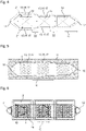
- Figures 1 and 2 each schematically show a cross-sectional view of a power semiconductor component according to an exemplary embodiment of the invention.
- Figures 2, 3 , 4, 5 and 6 each schematically show a top view of a power semiconductor component according to an exemplary embodiment of the invention.
- the power semiconductor component 1 comprises a cooling chamber 3.
- the cooling chamber 3 is formed of a cover 6, two sidewalls 8, a front 9, a back 10 and a bottom 7. These elements form a cooling cavity 18, through which a coolant substance can flow.
- the bottom 7 of the cooling chamber 3 is provided with an inlet port 11 and an outlet port 12.
- the inlet port 11 is arranged within the bottom 7 in a region close to the front 9 and the outlet port 12 is arranged in a region close to the back 10.
- the cooling chamber 3 is configured such that the coolant substance can flow through the cooling chamber 3 from the inlet port 11 to the outlet port 12.
- the cooling substance being a liquid coolant, for example, is pumped from the inlet port 11 through the cooling cavity 18 to the outlet port 12. This is to say that a flow direction of the coolant substance points from the inlet port 11 to the outlet port 12.
- the cooling chamber 3 comprises three openings 5 being arranged successively along the flow direction.
- the openings 5 are provided within the cover 6 of the cooling chamber 3 such that the openings 5 penetrate the cover 6 completely.
- each power semiconductor module 2 On each opening 5, one power semiconductor module 2 is arranged. For a better representability, only one power semiconductor module 2 is shown in Figure 1 . For example, each power semiconductor module 2 has a dimension in lateral directions being larger than a dimension in lateral directions of the associated opening 5.
- Each power semiconductor module 2 is provided with a cooling structure 4.
- the cooling structures 4 are formed of pin fins, extending in vertical direction.
- Each cooling structure 4 of each power semiconductor module 2 protrudes through the opening 5, on which the power semiconductor module 2 is arranged.
- the cooling structure 4 further protrudes into the cooling cavity 18 of the cooling chamber 3.
- each cooling structure 4 impedes an undisturbed flow of the cooling substance, and thus each cooling structure 4 forms a flow resistance region 14 for the cooling substance.
- the coolant substance experiences an increased flow resistance compared to regions, where no cooling structures 4 are present.
- the cooling chamber 3 comprises two bypass regions 17.
- each of the bypass regions 17 are connected in parallel to the two flow resistance regions 14 being closer to the inlet port 11.
- bypass regions 17 connected to the flow resistance regions 14 closer to the inlet port 11 are arranged on bottom surfaces 20 of the flow resistance regions 14.
- the bottom surfaces 20 of the flow resistance regions 14 are marked in connection with Figure 2 .
- Each bottom surface 20 of the flow resistance regions 14 faces the bottom 7 of the cooling chamber 3.
- Each bypass region 17 being arranged on the bottom surface 20 of the flow resistance region 14 comprises the recess within the bottom 7 of the cooling chamber 3.
- each recess 13 is arranged within the bottom 7 below one of the two openings 5 closer to the inlet port 11. Below the opening 5 closer to the outlet port 12, no recess 13 is arranged in the bottom 7.
- a volume of the recess within the bottom 15 closer to the inlet port 11 has a volume being larger than a volume of the recess within the bottom 15 closer to the outlet port 12.
- the recess within the bottom 15 closer to the inlet port 11 has a flow rate being larger than a flow rate of the recess within the bottom 15 closer to the outlet port 12.
- a flow rate of the flow resistance region 14, which is connected in parallel to the bypass region 17 closer to the inlet port 11 is smaller than a flow rate of the flow resistance region 14, which is connected in parallel to the bypass region 17 closer to the outlet port 12.
- the flow rate of the flow resistance region 14, which is connected in parallel to the bypass region 17 closer to the outlet port 12 is smaller than a flow rate of the flow resistance region 14 not provided with a bypass closer to the outlet port 12.
- each recess within the bottom 15 does not protrude beyond the flow resistance region 14 in flow direction and in lateral directions.
- each recess within the bottom 15 overlaps with the flow resistance region 14 completely in lateral directions.
- each length of each recess within the bottom 15 in flow direction is smaller than each length in flow direction of each flow resistance region 14.
- the volume of each bypass region 17 is, in this embodiment, dependent to each length of the recesses within the bottom 15.
- a recess within the bottom 15 closer to the inlet port 11 has a width perpendicular to the flow direction.
- the width of each of the recesses in the bottom 15 decreases in flow direction. This is to say that the width of the recess in the bottom 15 closer to the inlet port 11 decreases in flow direction and the width of the recess in the bottom 15 closer to the outlet port 12 decreases in flow direction.
- the cooling chamber 3 of the power semiconductor component 1 in connection with Figure 4 comprises two bypass regions 17, each connected in parallel to one of the flow resistance regions 14.
- Each bypass region 17 is arranged on two side surfaces 21 of the associated flow resistance regions 14 closer to the inlet port 11.
- Each side surface 21 of the flow resistance regions 14 faces one of the sidewalls of the cooling chamber 3.
- each bypass region 17 is arranged symmetrically around the associated flow resistance region 14 in lateral directions along the flow direction.
- the bypass region 17 closer to the inlet port 11 has a width perpendicular to the flow direction being larger than a width perpendicular to the flow direction of the bypass region 17 closer to the outlet port 12.
- the flow resistance region 14 closer to the outlet port 12 is not provided with any bypass region.
- Directly adjacent flow resistance regions 14 as well as directly adjacent bypass regions 17 are interconnected by an intermediate region 22 to one another.
- each bypass region 17 arranged on the side surface 21 of the flow resistance region 14 comprises a recess within the sidewall of the cooling chamber 3.
- Each width of each bypass region 17 declines in flow direction.
- the power semiconductor modules 2 according to Figure 6 each comprises twenty power semiconductor chips 19.
- the power semiconductor chips 19 are arranged within the power semiconductor modules along rows and columns.
- the power semiconductor chips 19 closer to the outlet port 12 of one power semiconductor module 2 can be cooled as effective as the power semiconductor chips 19 closer to the inlet port 11 of the same power semiconductor module 2.
Landscapes
- Cooling Or The Like Of Semiconductors Or Solid State Devices (AREA)
Abstract
Description
- The invention relates to a power semiconductor component.
- A critical issue in power electronics business is, for example, cooling of multiple power semiconductor modules. The way of cooling has a considerable impact on the current rating per chip of a power semiconductor module, and therefore, on the number of chips needed to achieve a certain power. If more than one power semiconductor module is used, the power semiconductor modules can be cooled down in a serial configuration. However, in such a serial configuration, a temperature of a coolant increases from an inlet port to an outlet port of a cooling chamber. Thus, the last semiconductor module closer to the outlet port is not cooled down as effectively as the first power semiconductor module closer to the inlet port. In addition, it is possible that a power semiconductor module closer to the inlet port is overcooled within such an arrangement.
- It is an object of the invention to provide a power semiconductor component having an improved reliability.
- The object is achieved by the subject-matter of the independent claim. Further exemplary embodiments are evident from the dependent claims and the following description.
- A first aspect of the invention relates to a power semiconductor component. The term "power" here and in the following, for example, refers to power semiconductor components, power semiconductor modules and/or power semiconductor chips adapted for processing voltages and currents of more than 100 V and/or more than 10 A, exemplary voltages up to 1200 V and current of several hundred amperes.
- The power semiconductor component has, for example, a main plane of extension. Lateral directions are aligned parallel to the main plane of extension and a vertical direction is aligned perpendicular to the main plane of extension.
- According to an embodiment of the invention, the power semiconductor component comprises at least two power semiconductor modules, each being connected to a cooling structure. For example, each power semiconductor module comprises a bottom surface on which a cooling structure is arranged.
- Each power semiconductor module is, for example, in direct contact to the cooling structure. Alternatively, a bond layer is arranged between each power semiconductor module and the cooling structure. The cooling structures are configured, for example, to increase an area of the bottom surface of the power semiconductor modules. The cooling structures are configured, exemplarily, to cool the power semiconductor modules during operation. The cooling structures comprise or consist, for example, of copper.
- Exemplarily, the cooling structures are formed from pin fins. For example, the pin fins are facing away from the power semiconductor modules. Each pin fin is formed from a pillar extending in vertical direction. For example, all of the pin fins have a common direction of extension being parallel to the vertical direction.
- Alternatively, the cooling structures are formed from lamellas. Each lamella extends in vertical direction having a tip facing away from the power semiconductor module. Further, each lamella of one of the power semiconductor modules extends in lateral direction over a width or a length of the power semiconductor module.
- According to the embodiment, the power semiconductor component comprises a cooling chamber having an inlet port and an outlet port. For example, the cooling chamber comprises a cover, at least two sidewalls, a front, a back and a bottom forming a cooling cavity. The at least two sidewalls are connected in lateral directions, for example, via the front and the back. The cover and the bottom are connected in vertical direction, for example, via the at least two sidewalls, the front and the back.
- Exemplarily, the front is provided with the inlet port and the back is provided with the outlet port. Alternatively, the bottom is provided with the inlet port and the outlet port. For example, in a region close to the front, the bottom is provided with the inlet port and in a region close to the back, the bottom is provided with the outlet port.
- According to the embodiment of the power semiconductor component, the cooling chamber is adapted for a flow direction of a coolant substance within the cooling chamber from the inlet port to the outlet port. For example, the cooling chamber, e.g., the cooling cavity, is configured such that a coolant substance can flow through the cooling chamber from the inlet port to the outlet port.
- The flow direction of the coolant substance is, for example parallel to a main extension direction of the cooling chamber, i.e., along a main extension direction of the sidewalls, the cover and the bottom.
- Exemplarily, the cooling substance is pumped from the inlet port through the cooling cavity to the outlet port. The cooling substance is, for example, a liquid coolant or a gas coolant. Exemplarily, heat generated during operation of the power semiconductor modules can be dissipated away via the cooling substance effectively.
- According to the embodiment of the power semiconductor component, each of the at least two cooling structures are formed within the cooling chamber consecutively in direction of the flow direction such that each of the at least two cooling structures forms a flow resistance region in the cooling chamber. Each cooling structure is configured, exemplarily, to form a flow resistance for the cooling substance flowing from the inlet port to the outlet port. This is to say that each cooling structure associated to one power semiconductor module forms one flow resistance region. Exemplarily, a flow resistance of a flow resistant region is higher than a flow resistance between two consecutive flow resistance regions.
- According to the embodiment of the power semiconductor component, the cooling chamber comprises at least one bypass region. For example, the bypass region is free of any cooling structures. Exemplarily, the flow resistance of a bypass region is smaller than the flow resistance of the flow resistance regions.
- According to the embodiment of a power semiconductor component, the at least one bypass region is connected in parallel to at least one of the at least two flow resistance regions being closer to the inlet port. For example, the bypass region is connected in parallel to the flow resistance region being closest to the inlet port.
- Exemplarily, the bypass region connected in parallel to the flow resistance region is arranged in direct contact to the flow resistance region. This is to say that between the bypass region and the flow resistance region no additional element is arranged, for example.
- According to the embodiment of the power semiconductor component, the cooling chamber is adapted for a flow rate of the at least one flow resistance region, which is connected in parallel to the at least one bypass region, closer to the inlet port being smaller than the flow rate of one of the at least two flow resistance regions closer to the outlet port.
- In summary, such a power semiconductor component having a bypass region can provide, inter alia, the following advantages. Exemplarily, the power semiconductor modules being arranged along the flow direction can be cooled down effectively. Further, an overcooling of the power semiconductor modules close to the inlet port can be avoided, for example. In addition, a temperature distribution across all of the power semiconductor modules is more equalized than without the bypass.
- Moreover, due to such a bypass region a flow resistance of the whole power semiconductor component is reduced, for example, leading to a modified operation point of a pump of the coolant substance. This is to say that a higher flow rate through the cooling chamber can be achieved. Thus, a higher current rating of the power semiconductor modules can be increased without any modification of the design of the power semiconductor modules. This is exemplarily translated into a longer lifetime and thus a better reliability of the power semiconductor component without being more expensive.
- Further, it is conceivable that at least two power semiconductor components are arranged adjacent to one another such that the flow directions are parallel. In such an arrangement, the inlet port is a common inlet port and the outlet port is common outlet port for the two power semiconductor components.
- According to at least one embodiment of the power semiconductor component, the at least one bypass region connected to at least one of the at least two flow resistance regions is interconnected by at least one intermediate region to one of the at least two flow resistance regions closer to the outlet port. For example, the intermediate region is free of any additional structures, e.g. cooling structures, within the cooling cavity. For example, the intermediate region is configured such that a velocity through a cross-section of the intermediate region perpendicular to the flow direction is substantially constant at any point of the cross section. Substantially constant means here that the velocity does not deviate from an average value of at most 10 %.
- The coolant substance leaving the bypass region and the associated flow resistance region, for example, are intermixed within the intermediate region. This exemplarily leads to a temperature decrease of the coolant substance leaving the flow resistance region associated to the bypass.
- According to at least one embodiment of the power semiconductor component, the cooling chamber comprise at least one opening.
- According to at least one embodiment of the power semiconductor component, one of the at least two cooling structures protrudes through the at least one opening into the cooling chamber and the other of the at least two cooling structures are formed integrally with the cooling chamber.
- According to at least one embodiment of the power semiconductor component, the cooling chamber comprises at least two openings. For example, the opening, exemplarily each of the openings, is provided within the cover of the cooling chamber. Exemplarily, each opening penetrates the cover of the cooling chamber completely.
- According to at least one embodiment of the power semiconductor component, the at least two openings are arranged in the cooling chamber consecutively in the direction of the flow direction. For example, the openings are spaced apart from one another in lateral directions, e.g., along the flow direction.
- According to at least one embodiment of the power semiconductor component, each of the at least two cooling structures protrudes through one of the at least two openings into the cooling chamber. Each of the cooling structures protruding through the opening into the cooling chamber forms one of the flow resistance regions.
- For example, one of the power semiconductor modules is arranged on one of the openings such that the cooling structures penetrate through the opening of the cooling chamber. Exemplarily, each power semiconductor module has a dimension in lateral directions being at least 5 % larger than a dimension in lateral directions of the opening, on which the power semiconductor module is arranged.
- According to at least one embodiment of the power semiconductor component, each of the at least two cooling structures are formed integrally with the cooling chamber. Thus, the cooling structures are a part of the cooling chamber. In this case, each semiconductor module is arranged directly and exclusively on the cooling chamber in the region of one of the cooling structures. In this embodiment the cooling chamber is exemplarily formed as a closed cooler.
- According to at least one embodiment of the power semiconductor component, the at least one bypass region connected to one of the at least two flow resistance regions is arranged on at least one side surface of the flow resistance region. The side surface of the flow resistance region faces, for example, one of the sidewalls of the cooling chamber. In this embodiment, the bypass region is exemplarily arranged in lateral directions next to the flow resistance region.
- For example, the bypass region connected to one of the at least two flow resistance regions is arranged on at least two side surfaces of the flow resistance region. In this case, the bypass region is arranged symmetrically around the flow resistance region in lateral directions along the flow direction.
- According to at least one embodiment of the power semiconductor component, the at least one bypass region connected to one of the at least two flow resistance regions is arranged on a bottom surface of the flow resistance region. The bottom surface of the flow resistance region faces, for example, the bottom of the cooling chamber. In this embodiment, the bypass region is exemplarily arranged in vertical direction below the flow resistance region.
- According to at least one embodiment of the power semiconductor component, the at least one bypass region connected to one of the at least two flow resistance regions is arranged on the at least one side surface and on the bottom surface of the flow resistance region.
- According to at least one embodiment of the power semiconductor component, the at least one bypass region being arranged on the bottom surface of the flow resistance region comprises a recess within a bottom of the cooling chamber. In this embodiment, the bypass region arranged on the bottom surface of the flow resistance region is exemplarily formed between a main surface of the recess delimited by the bottom of the cooling chamber and the bottom surface of the flow resistance region.
- According to at least one embodiment of the power semiconductor component, the at least one bypass region being arranged on the side surface of the flow resistance region comprises a recess within a sidewall of the cooling chamber. In this embodiment, the bypass region arranged on the side surface of the flow resistance region is formed between a main surface of the recess delimited by the sidewall of the cooling chamber and the side surface of the flow resistance region.
- For example, due to production tolerances, there is a gap between the cooling structures and the bottom of the cooling chamber. Further, due to production tolerances, there is a gap between the cooling structures and the sidewall of the cooling chamber. However, if the bottom and/or the sidewall does not comprise a recess, those gaps cannot be identified with a bypass. For example, a flow rate of a coolant passing one of the gaps is more than one order of magnitude smaller than a flow rate of a coolant passing the bypass region.
- Exemplarily, the bypass region arranged on the bottom surface of the flow resistance region is formed by the recess within the bottom as well as the gap between the recess within the bottom and the bottom surface of the flow resistance region. Alternatively or in addition, the bypass region arranged on the side surface of the flow resistance region is formed by the recess within the sidewall as well as the gap between the recess within the sidewall and the side surface of the flow resistance region.
- According to at least one embodiment of the power semiconductor component, the recess within the bottom does not protrude beyond the flow resistance region in flow direction. For example, the recess within the bottom overlaps with the flow resistance region completely in lateral directions. Further, a cross-section of the recess within the bottom in lateral directions is smaller than a cross-section in lateral directions of the flow resistance region.
- According to at least one embodiment of the power semiconductor component, a main surface of the recess within the bottom is inclined with respect to a main extension plane of the power semiconductor component. For example, a distance between the main surface of the recess within the bottom and the bottom surface of the flow resistance region decreases in size in flow direction. The distance is decreased in size, for example, linearly or non-linearly.
- According to at least one embodiment, the power semiconductor component comprises at least three power semiconductor modules, each being connected to a cooling structure, wherein the cooling chamber comprises at least two bypass regions.
- According to at least one embodiment of the power semiconductor component, each of the at least two flow resistance regions being closer to the outlet port are connected in parallel to one of the at least two bypass regions.
- According to at least one embodiment of the power semiconductor component, a flow rate of one of the at least two bypass regions closer to the inlet port is larger than a flow rate of one of the at least two bypass regions closer to the outlet port.
- According to at least one embodiment of the power semiconductor component, a volume of the recess in the bottom closer to the inlet port is larger than a volume of the recess in the bottom closer to the outlet port. Exemplarily, a volume of the bypass region arranged on the bottom surface of the flow resistance region closer to the inlet port is larger than a volume of the bypass region arranged on the bottom surface of the flow resistance region closer to the outlet port.
- According to at least one embodiment of the power semiconductor component, each recess in the bottom comprises a length parallel to the flow direction and the lengths of consecutive recesses within the bottom decrease in flow direction. For example, the length of the recess in the bottom is a minimal expansion of the recess in the bottom of the cooling chamber in lateral directions parallel to the flow direction.
- According to at least one embodiment of the power semiconductor component, each recess in the bottom comprises a width perpendicular to the flow direction and the width of each recess in the bottom decreases in flow direction. For example, the width of the recess in the bottom is a minimal expansion of the recess in the bottom of the cooling chamber in lateral directions perpendicular to the flow direction.
- Exemplarily, the volume of the recess in the bottom is dependent on at least one of the length and the width of the recess in the bottom. Further, the volume of the bypass region arranged on the bottom surface of the flow resistance region is dependent on at least one of the length and the width of the recess in the bottom.
- According to at least one embodiment of the power semiconductor component, a volume of the recess within the sidewall closer to the inlet port is larger than a volume of the recess within the sidewall closer to the outlet port. Exemplarily, a volume of the bypass region arranged on the side surface of the flow resistance region closer to the inlet port is larger than a volume of the bypass region arranged on the side surface of the flow resistance region closer to the outlet port.
- According to at least one embodiment of the power semiconductor component, each recess within the sidewall comprises a width perpendicular to the flow direction and the width of each consecutive recess within the sidewall decreases in flow direction. For example, the width of the recess within the sidewall is a minimal expansion between the side surface of the flow resistance region and the recess within the sidewall of the cooling chamber in lateral directions perpendicular to the flow direction.
- According to at least one embodiment of the power semiconductor component, each recess within the sidewall comprises a length parallel to the flow direction and the length of each consecutive recess within the sidewall decrease in flow direction. For example, the length of the recess within the sidewall is a minimal expansion of the recess in the sidewall of the cooling chamber in lateral directions along the flow direction.
- Exemplarily, the volume of the recess within the sidewall is dependent on at least one of the length and the width of the recess within the sidewall.
- It is further possible that the width of one of the recesses within the sidewall decreases in flow direction. E.g. a distance between the main surface of the recess within the sidewall and the side surface of the flow resistance region decreases in size in flow direction. The distance is decreased in size, for example, linearly or non-linearly.
- According to at least one embodiment of the power semiconductor component, cross-sections perpendicular to the flow direction of consecutive bypass regions are reduced in flow direction by at least 20 %.
- According to at least one embodiment of the power semiconductor component, a cross-section perpendicular to the flow direction of each bypass region is at least 5 % and at most 50 % of a total cross-section perpendicular to the flow direction comprising the bypass region and the flow resistance region.
- According to at least one embodiment of the power semiconductor component, each power semiconductor module comprises at least one power semiconductor chip.
- For example, each power semiconductor module comprises a plurality of power semiconductor chips. The power semiconductor chips are arranged spaced apart from one another in lateral directions. For example, the power semiconductor chips are arranged on grid points of a regular or non-regular grid. For example, the power semiconductor chips are arranged along rows and columns.
- If the power semiconductor module comprises the plurality of power semiconductor chips, the bypass region arranged on the bottom surface of the flow resistance region is, for example, inclined with respect to a main extension plane of the power semiconductor component. Due to such an arrangement, a flow rate within the flow resistance region can be predefined by the distance of the main surface of the recess in the bottom of the cooling chamber and the bottom surface of the flow resistance region. If the distance decreases in flow direction, the flow rate within the flow resistance region increases closer to the outlet port. Thus, also power semiconductor chips, being comprised of one of the power semiconductor modules, arranged closer to the outlet port can be cooled effectively.
- For example, the recess within the bottom extends in lateral directions along the flow direction up to a centre of the power semiconductor chip closer to the outlet port. Exemplarily, the recess within the bottom ends at least 1 mm to at least 5 mm before the centre of the power semiconductor chip closer to the outlet port in lateral directions along the flow direction.
- The subject-matter of the invention will be explained in more detail in the following with reference to exemplary embodiments which are illustrated in the attached drawings.
-
Figures 1 and 2 each schematically show a cross-sectional view of a power semiconductor component according to an exemplary embodiment of the invention. -
Figures 2, 3 ,4, 5 and 6 each schematically show a top view of a power semiconductor component according to an exemplary embodiment of the invention. - The reference symbols used in the drawings and their meanings are listed in summary in the list of reference symbols. In principle, identical parts are provided with the same reference symbols in the figures.
- The power semiconductor component 1 according to the exemplary embodiment of
Figure 1 comprises acooling chamber 3. The coolingchamber 3 is formed of acover 6, twosidewalls 8, a front 9, a back 10 and abottom 7. These elements form acooling cavity 18, through which a coolant substance can flow. Thebottom 7 of thecooling chamber 3 is provided with aninlet port 11 and anoutlet port 12. Theinlet port 11 is arranged within thebottom 7 in a region close to the front 9 and theoutlet port 12 is arranged in a region close to the back 10. - The cooling
chamber 3 is configured such that the coolant substance can flow through thecooling chamber 3 from theinlet port 11 to theoutlet port 12. The cooling substance, being a liquid coolant, for example, is pumped from theinlet port 11 through thecooling cavity 18 to theoutlet port 12. This is to say that a flow direction of the coolant substance points from theinlet port 11 to theoutlet port 12. - Furthermore, the cooling
chamber 3 comprises threeopenings 5 being arranged successively along the flow direction. Here, theopenings 5 are provided within thecover 6 of thecooling chamber 3 such that theopenings 5 penetrate thecover 6 completely. - On each
opening 5, onepower semiconductor module 2 is arranged. For a better representability, only onepower semiconductor module 2 is shown inFigure 1 . For example, eachpower semiconductor module 2 has a dimension in lateral directions being larger than a dimension in lateral directions of the associatedopening 5. - Each
power semiconductor module 2 is provided with acooling structure 4. In this embodiment, the coolingstructures 4 are formed of pin fins, extending in vertical direction. Eachcooling structure 4 of eachpower semiconductor module 2 protrudes through theopening 5, on which thepower semiconductor module 2 is arranged. Thecooling structure 4 further protrudes into thecooling cavity 18 of thecooling chamber 3. - During operation of the power semiconductor component 1, the coolant substance is pumped in flow direction through the
cooling chamber 3. Hereby, each coolingstructure 4 impedes an undisturbed flow of the cooling substance, and thus each coolingstructure 4 forms aflow resistance region 14 for the cooling substance. Within such aflow resistance region 14, the coolant substance experiences an increased flow resistance compared to regions, where no coolingstructures 4 are present. - Furthermore, according to this embodiment, the cooling
chamber 3 comprises twobypass regions 17. Here, each of thebypass regions 17 are connected in parallel to the twoflow resistance regions 14 being closer to theinlet port 11. - In this embodiment, the
bypass regions 17 connected to theflow resistance regions 14 closer to theinlet port 11 are arranged onbottom surfaces 20 of theflow resistance regions 14. The bottom surfaces 20 of theflow resistance regions 14 are marked in connection withFigure 2 . Eachbottom surface 20 of theflow resistance regions 14 faces thebottom 7 of thecooling chamber 3. Eachbypass region 17 being arranged on thebottom surface 20 of theflow resistance region 14 comprises the recess within thebottom 7 of thecooling chamber 3. - In this embodiment, two recesses 13 are arranged within the
bottom 7 of thecooling chamber 3. Each recess 13 is arranged within thebottom 7 below one of the twoopenings 5 closer to theinlet port 11. Below theopening 5 closer to theoutlet port 12, no recess 13 is arranged in thebottom 7. - A volume of the recess within the bottom 15 closer to the
inlet port 11 has a volume being larger than a volume of the recess within the bottom 15 closer to theoutlet port 12. Thus, the recess within the bottom 15 closer to theinlet port 11 has a flow rate being larger than a flow rate of the recess within the bottom 15 closer to theoutlet port 12. Furthermore, a flow rate of theflow resistance region 14, which is connected in parallel to thebypass region 17 closer to theinlet port 11 is smaller than a flow rate of theflow resistance region 14, which is connected in parallel to thebypass region 17 closer to theoutlet port 12. In addition, the flow rate of theflow resistance region 14, which is connected in parallel to thebypass region 17 closer to theoutlet port 12, is smaller than a flow rate of theflow resistance region 14 not provided with a bypass closer to theoutlet port 12. - In connection with
Figure 2 , a cross-sectional view along the flow direction, also depicted inFigure 1 , is shown. Here, threepower semiconductor modules 2 are shown explicitly. - Each recess within the bottom 15 does not protrude beyond the
flow resistance region 14 in flow direction and in lateral directions. Here, each recess within the bottom 15 overlaps with theflow resistance region 14 completely in lateral directions. Further, each length of each recess within the bottom 15 in flow direction is smaller than each length in flow direction of eachflow resistance region 14. The volume of eachbypass region 17 is, in this embodiment, dependent to each length of the recesses within the bottom 15. - In connection with
Figure 3 , the twopower semiconductor modules 2 closer to theinlet port 11 are not shown, as inFigure 1 . A recess within the bottom 15 closer to theinlet port 11 has a width perpendicular to the flow direction. Here, the width of each of the recesses in the bottom 15 decreases in flow direction. This is to say that the width of the recess in the bottom 15 closer to theinlet port 11 decreases in flow direction and the width of the recess in the bottom 15 closer to theoutlet port 12 decreases in flow direction. - The cooling
chamber 3 of the power semiconductor component 1 in connection withFigure 4 comprises twobypass regions 17, each connected in parallel to one of theflow resistance regions 14. Eachbypass region 17 is arranged on two side surfaces 21 of the associatedflow resistance regions 14 closer to theinlet port 11. Each side surface 21 of theflow resistance regions 14 faces one of the sidewalls of thecooling chamber 3. In this embodiment, eachbypass region 17 is arranged symmetrically around the associatedflow resistance region 14 in lateral directions along the flow direction. - The
bypass region 17 closer to theinlet port 11 has a width perpendicular to the flow direction being larger than a width perpendicular to the flow direction of thebypass region 17 closer to theoutlet port 12. - The
flow resistance region 14 closer to theoutlet port 12 is not provided with any bypass region. - Directly adjacent
flow resistance regions 14 as well as directlyadjacent bypass regions 17 are interconnected by anintermediate region 22 to one another. - According to
Figure 5 , eachbypass region 17 arranged on the side surface 21 of theflow resistance region 14 comprises a recess within the sidewall of thecooling chamber 3. Each width of eachbypass region 17 declines in flow direction. - The
power semiconductor modules 2 according toFigure 6 each comprises twenty power semiconductor chips 19. The power semiconductor chips 19 are arranged within the power semiconductor modules along rows and columns. - Due to the shape of the
bypass regions 17 arranged on the bottom 7 surface of theflow resistance region 14, the power semiconductor chips 19 closer to theoutlet port 12 of onepower semiconductor module 2 can be cooled as effective as the power semiconductor chips 19 closer to theinlet port 11 of the samepower semiconductor module 2. -
- 1
- power semiconductor component
- 2
- power semiconductor module
- 3
- cooling chamber
- 4
- cooling structure
- 5
- opening
- 6
- cover
- 7
- bottom
- 8
- sidewall
- 9
- front
- 10
- back
- 11
- inlet port
- 12
- outlet port
- 13
- recess
- 14
- flow resistance region
- 15
- recess within the bottom
- 16
- recess within the sidewall
- 17
- bypass region
- 18
- cooling cavity
- 19
- power semiconductor chip
- 20
- bottom surface
- 21
- side surface
- 22
- intermediate region
- C
- flow direction
Claims (15)
- A power semiconductor component (1), with- at least two power semiconductor modules (2), each being connected to a cooling structure (4), and- a cooling chamber (3) having an inlet port (11) and an outlet port (12), wherein- the cooling chamber (3) is adapted for a flow direction of a coolant substance within the cooling chamber (3) from the inlet port (11) to the outlet port (12),- each of the at least two cooling structures (4) are provided within the cooling chamber (3) consecutively in direction of the flow direction such that each of the at least two cooling structures (4) forms a flow resistance region (14) in the cooling chamber (3),- the cooling chamber (3) comprises at least one bypass region (17),- the at least one bypass region (17) is connected in parallel to at least one of the at least two flow resistance regions (14) being closer to the inlet port (11), and- the cooling chamber (3) is adapted for a flow rate of the at least one flow resistance region (14), which is connected in parallel to the at least one bypass region (17), closer to the inlet port (11) being smaller than a flow rate of one of the at least two flow resistance regions (14) closer to the outlet port (12).
- The power semiconductor component (1) according to the preceding claim, wherein the at least one bypass region (17) connected to one of the at least two flow resistance regions (14) is interconnected by at least one intermediate region (22) to one of the at least two flow resistance regions (14) closer to the outlet port (12).
- The power semiconductor component (1) according to one of the preceding claims, wherein- the cooling chamber (3) comprise at least one opening (5),- one of the at least two cooling structures (4) protrudes through the at least one opening (5) into the cooling chamber (3), and- the other of the at least two cooling structures (4) are formed integrally with the cooling chamber.
- The power semiconductor component (1) according to one of the preceding claims, wherein the at least one bypass region (17) connected to one of the at least two flow resistance regions (14) is arranged on at least one side surface (21) of the flow resistance region (14).
- The power semiconductor component (1) according to one of claims 1 to 3, wherein the at least one bypass region (17) connected to one of the at least two flow resistance regions (14) is arranged on a bottom surface (20) of the flow resistance region (14).
- The power semiconductor component (1) according to one of claims 1 to 3, wherein the at least one bypass region (17) connected to one of the at least two flow resistance regions (14) is arranged on the at least one side surface (21) and on the bottom surface (20) of the flow resistance region (14).
- The power semiconductor component (1) according to one of the claims 5 or 6, wherein- the at least one bypass region (17) being arranged on the bottom surface (20) of the flow resistance region (14) comprises a recess within a bottom (6) of the cooling chamber (3), and- the recess within the bottom (15) does not protrude beyond the flow resistance region (14) in flow direction.
- The power semiconductor component (1) according to claim 7, wherein a main surface of the recess within the bottom (15) is inclined with respect to a main extension plane of the power semiconductor component (1).
- The power semiconductor component (1) according to one of the preceding claims comprising- at least three power semiconductor modules (2), each being connected to a cooling structure (4), wherein- the cooling chamber (3) comprises at least two bypass regions (17),- each of the at least two flow resistance regions (14) being closer to the outlet port (12) are connected in parallel to one of the at least two bypass regions (17),- a flow rate of one of the at least two bypass regions (17) closer to the inlet port (11) is larger than a flow rate of one of the at least two bypass regions (17) closer to the outlet port (12).
- The power semiconductor component (1) according the claims 7 and 9, wherein a volume of the recess within the bottom (15) closer to the inlet port (11) is larger than a volume of the recess within the bottom (15) closer to the outlet port (12).
- The power semiconductor component (1) according to one of the claims 7 and 9 or 10, wherein at least one of- each recess within the bottom (15) comprises a length parallel to the flow direction and the lengths of consecutive recesses within the bottom (15) decrease in flow direction, and- each recess within the bottom (15) comprises a width perpendicular to the flow direction and the width of each recess within the bottom (15) decreases in flow direction.
- The power semiconductor component (1) according to one of the claims 9 to 11, wherein- the at least one bypass region (17) being arranged on the side surface (21) of the flow resistance region (14) is formed as a recess within a sidewall of the cooling chamber (3), and- a volume of the recess within the sidewall closer to the inlet port (11) is larger than a volume of the recess within the sidewall closer to the outlet port (12).
- The power semiconductor component (1) according to claim 12, wherein at least one of- each recess within the sidewall comprises a width perpendicular to the flow direction and the width of each consecutive recess within the sidewall decreases in flow direction, and- each recess within the sidewall comprises a length parallel to the flow direction and the length of each consecutive recess within the sidewall decrease in flow direction.
- The power semiconductor component (1) according to claims 9 to 13, wherein at least one of- cross sections perpendicular to the flow direction of consecutive bypass regions (17) are reduced in flow direction by at least 20%, and- a cross section perpendicular to the flow direction of each bypass region (17) is at least 5% and at most 50% of a total cross section perpendicular to the flow direction comprising the bypass region (17) and the flow resistance region (14).
- The power semiconductor component (1) according to one of the preceding claims, wherein each power semiconductor module (2) comprises at least one power semiconductor chip (19).
Priority Applications (5)
| Application Number | Priority Date | Filing Date | Title |
|---|---|---|---|
| EP20210025.1A EP4006968B1 (en) | 2020-11-26 | 2020-11-26 | Power semiconductor component |
| PCT/EP2021/082840 WO2022112339A2 (en) | 2020-11-26 | 2021-11-24 | Power semiconductor component |
| JP2023532187A JP7644236B2 (en) | 2020-11-26 | 2021-11-24 | Power Semiconductor Components |
| US18/038,545 US12494409B2 (en) | 2020-11-26 | 2021-11-24 | Power semiconductor component |
| CN202180079384.9A CN116490970B (en) | 2020-11-26 | 2021-11-24 | Power semiconductor components |
Applications Claiming Priority (1)
| Application Number | Priority Date | Filing Date | Title |
|---|---|---|---|
| EP20210025.1A EP4006968B1 (en) | 2020-11-26 | 2020-11-26 | Power semiconductor component |
Publications (2)
| Publication Number | Publication Date |
|---|---|
| EP4006968A1 true EP4006968A1 (en) | 2022-06-01 |
| EP4006968B1 EP4006968B1 (en) | 2023-03-22 |
Family
ID=73642556
Family Applications (1)
| Application Number | Title | Priority Date | Filing Date |
|---|---|---|---|
| EP20210025.1A Active EP4006968B1 (en) | 2020-11-26 | 2020-11-26 | Power semiconductor component |
Country Status (5)
| Country | Link |
|---|---|
| US (1) | US12494409B2 (en) |
| EP (1) | EP4006968B1 (en) |
| JP (1) | JP7644236B2 (en) |
| CN (1) | CN116490970B (en) |
| WO (1) | WO2022112339A2 (en) |
Cited By (1)
| Publication number | Priority date | Publication date | Assignee | Title |
|---|---|---|---|---|
| WO2024240854A1 (en) * | 2023-05-24 | 2024-11-28 | Erwin Quarder Systemtechnik Gmbh | Cooling component |
Families Citing this family (1)
| Publication number | Priority date | Publication date | Assignee | Title |
|---|---|---|---|---|
| DE102024205942B3 (en) * | 2024-06-26 | 2025-12-11 | Schaeffler Technologies AG & Co. KG | Cooler for a power electronic arrangement and power electronic arrangement |
Citations (4)
| Publication number | Priority date | Publication date | Assignee | Title |
|---|---|---|---|---|
| US6400012B1 (en) * | 1997-09-17 | 2002-06-04 | Advanced Energy Voorhees, Inc. | Heat sink for use in cooling an integrated circuit |
| JP2004080856A (en) * | 2002-08-12 | 2004-03-11 | Hitachi Ltd | Power converter |
| EP2824703A1 (en) * | 2012-10-29 | 2015-01-14 | Fuji Electric Co., Ltd. | Semiconductor device |
| JP2016062919A (en) * | 2014-09-12 | 2016-04-25 | 株式会社ティラド | heatsink |
Family Cites Families (11)
| Publication number | Priority date | Publication date | Assignee | Title |
|---|---|---|---|---|
| US5810072A (en) | 1995-09-08 | 1998-09-22 | Semipower Systems, Inc. | Forced air cooler system |
| DK176137B1 (en) | 2003-10-27 | 2006-09-25 | Danfoss Silicon Power Gmbh | Flow distribution unit and cooling unit with bypass flow |
| JP2009092357A (en) | 2007-10-12 | 2009-04-30 | Showa Denko Kk | Tabular heat pipe |
| JP2013197159A (en) * | 2012-03-16 | 2013-09-30 | Ihi Corp | Cooling device |
| TWI482244B (en) | 2012-11-19 | 2015-04-21 | 財團法人工業技術研究院 | Heat exchanger and semiconductor module |
| DE102013209719B4 (en) * | 2013-05-24 | 2016-07-07 | Infineon Technologies Ag | Power semiconductor module with liquid cooling |
| JP6117361B2 (en) | 2013-08-23 | 2017-04-19 | 日立オートモティブシステムズ株式会社 | Power converter |
| WO2016194158A1 (en) | 2015-06-03 | 2016-12-08 | 三菱電機株式会社 | Liquid-cooled cooler, and manufacturing method for radiating fin in liquid-cooled cooler |
| JP6929788B2 (en) | 2015-12-04 | 2021-09-01 | ローム株式会社 | Power module equipment and electric or hybrid vehicles |
| CN111653529B (en) * | 2020-04-30 | 2022-05-10 | 华为数字能源技术有限公司 | A liquid cooling radiator and communication equipment |
| US11525638B2 (en) * | 2020-10-19 | 2022-12-13 | Dana Canada Corporation | High-performance heat exchanger with calibrated bypass |
-
2020
- 2020-11-26 EP EP20210025.1A patent/EP4006968B1/en active Active
-
2021
- 2021-11-24 CN CN202180079384.9A patent/CN116490970B/en active Active
- 2021-11-24 JP JP2023532187A patent/JP7644236B2/en active Active
- 2021-11-24 WO PCT/EP2021/082840 patent/WO2022112339A2/en not_active Ceased
- 2021-11-24 US US18/038,545 patent/US12494409B2/en active Active
Patent Citations (4)
| Publication number | Priority date | Publication date | Assignee | Title |
|---|---|---|---|---|
| US6400012B1 (en) * | 1997-09-17 | 2002-06-04 | Advanced Energy Voorhees, Inc. | Heat sink for use in cooling an integrated circuit |
| JP2004080856A (en) * | 2002-08-12 | 2004-03-11 | Hitachi Ltd | Power converter |
| EP2824703A1 (en) * | 2012-10-29 | 2015-01-14 | Fuji Electric Co., Ltd. | Semiconductor device |
| JP2016062919A (en) * | 2014-09-12 | 2016-04-25 | 株式会社ティラド | heatsink |
Cited By (1)
| Publication number | Priority date | Publication date | Assignee | Title |
|---|---|---|---|---|
| WO2024240854A1 (en) * | 2023-05-24 | 2024-11-28 | Erwin Quarder Systemtechnik Gmbh | Cooling component |
Also Published As
| Publication number | Publication date |
|---|---|
| CN116490970B (en) | 2024-07-26 |
| CN116490970A (en) | 2023-07-25 |
| US12494409B2 (en) | 2025-12-09 |
| WO2022112339A3 (en) | 2022-07-21 |
| EP4006968B1 (en) | 2023-03-22 |
| JP7644236B2 (en) | 2025-03-11 |
| JP2023548625A (en) | 2023-11-17 |
| WO2022112339A2 (en) | 2022-06-02 |
| US20240096746A1 (en) | 2024-03-21 |
Similar Documents
| Publication | Publication Date | Title |
|---|---|---|
| KR101906646B1 (en) | Cooler for semiconductor module, and semiconductor module | |
| JP5900610B2 (en) | Semiconductor device and cooler for semiconductor device | |
| US12494409B2 (en) | Power semiconductor component | |
| US9220182B2 (en) | Semiconductor module cooler and semiconductor module | |
| US20200286812A1 (en) | Heatsink, and semiconductor module including the heatsink | |
| US20140284029A1 (en) | Cooler | |
| US20140043765A1 (en) | Semiconductor module cooler and semiconductor module | |
| US20190148265A1 (en) | Semiconductor module | |
| US20160313072A1 (en) | Heat sink for cooling plurality of heat generating components | |
| US20240381567A1 (en) | Cooler for cooling power electronics | |
| JP2009176881A (en) | Cooling apparatus | |
| US20190080985A1 (en) | Liquid-cooled type cooling device | |
| EP2833403B1 (en) | Header for electronic cooler | |
| US20240381569A1 (en) | Cooler for cooling power electronics | |
| US20250218896A1 (en) | Heat dissipation member, cooling device, and semiconductor module | |
| WO2023171529A1 (en) | Cooling device, heat-dissipating member, and semiconductor module | |
| CN116895616A (en) | cooling device | |
| JP2015149361A (en) | Cooler | |
| CN116364676A (en) | Heat sink and cooling device | |
| JP2020004766A (en) | Cooler | |
| US20260082526A1 (en) | Cooling component for heat dissipation | |
| JP2021052060A (en) | Heat sink and electronic apparatus with heat sink | |
| US20250210445A1 (en) | Heat dissipation member and semiconductor module | |
| CN217336255U (en) | Cooler and cooled electrical device assembly | |
| EP4199077B1 (en) | Flow inverter and power semiconductor component |
Legal Events
| Date | Code | Title | Description |
|---|---|---|---|
| PUAI | Public reference made under article 153(3) epc to a published international application that has entered the european phase |
Free format text: ORIGINAL CODE: 0009012 |
|
| STAA | Information on the status of an ep patent application or granted ep patent |
Free format text: STATUS: THE APPLICATION HAS BEEN PUBLISHED |
|
| AK | Designated contracting states |
Kind code of ref document: A1 Designated state(s): AL AT BE BG CH CY CZ DE DK EE ES FI FR GB GR HR HU IE IS IT LI LT LU LV MC MK MT NL NO PL PT RO RS SE SI SK SM TR |
|
| RIN1 | Information on inventor provided before grant (corrected) |
Inventor name: BEYER, HARALD Inventor name: TRUESSEL, DOMINIK Inventor name: MALEKI, MILAD Inventor name: HARTMANN, SAMUEL Inventor name: SANTOLARIA, LLUIS |
|
| STAA | Information on the status of an ep patent application or granted ep patent |
Free format text: STATUS: REQUEST FOR EXAMINATION WAS MADE |
|
| RIN1 | Information on inventor provided before grant (corrected) |
Inventor name: BEYER, HARALD Inventor name: TRUESSEL, DOMINIK Inventor name: MALEKI, MILAD Inventor name: HARTMANN, SAMUEL Inventor name: SANTOLARIA, LLUIS |
|
| 17P | Request for examination filed |
Effective date: 20220705 |
|
| RBV | Designated contracting states (corrected) |
Designated state(s): AL AT BE BG CH CY CZ DE DK EE ES FI FR GB GR HR HU IE IS IT LI LT LU LV MC MK MT NL NO PL PT RO RS SE SI SK SM TR |
|
| GRAP | Despatch of communication of intention to grant a patent |
Free format text: ORIGINAL CODE: EPIDOSNIGR1 |
|
| STAA | Information on the status of an ep patent application or granted ep patent |
Free format text: STATUS: GRANT OF PATENT IS INTENDED |
|
| INTG | Intention to grant announced |
Effective date: 20221019 |
|
| RIN1 | Information on inventor provided before grant (corrected) |
Inventor name: BEYER, HARALD Inventor name: TRUESSEL, DOMINIK Inventor name: MALEKI, MILAD Inventor name: HARTMANN, SAMUEL Inventor name: SANTOLARIA, LLUIS |
|
| GRAS | Grant fee paid |
Free format text: ORIGINAL CODE: EPIDOSNIGR3 |
|
| GRAA | (expected) grant |
Free format text: ORIGINAL CODE: 0009210 |
|
| STAA | Information on the status of an ep patent application or granted ep patent |
Free format text: STATUS: THE PATENT HAS BEEN GRANTED |
|
| AK | Designated contracting states |
Kind code of ref document: B1 Designated state(s): AL AT BE BG CH CY CZ DE DK EE ES FI FR GB GR HR HU IE IS IT LI LT LU LV MC MK MT NL NO PL PT RO RS SE SI SK SM TR |
|
| REG | Reference to a national code |
Ref country code: GB Ref legal event code: FG4D |
|
| REG | Reference to a national code |
Ref country code: CH Ref legal event code: EP |
|
| REG | Reference to a national code |
Ref country code: IE Ref legal event code: FG4D |
|
| REG | Reference to a national code |
Ref country code: DE Ref legal event code: R096 Ref document number: 602020009006 Country of ref document: DE |
|
| REG | Reference to a national code |
Ref country code: AT Ref legal event code: REF Ref document number: 1555819 Country of ref document: AT Kind code of ref document: T Effective date: 20230415 |
|
| REG | Reference to a national code |
Ref country code: LT Ref legal event code: MG9D |
|
| P01 | Opt-out of the competence of the unified patent court (upc) registered |
Effective date: 20230527 |
|
| REG | Reference to a national code |
Ref country code: NL Ref legal event code: MP Effective date: 20230322 |
|
| PG25 | Lapsed in a contracting state [announced via postgrant information from national office to epo] |
Ref country code: RS Free format text: LAPSE BECAUSE OF FAILURE TO SUBMIT A TRANSLATION OF THE DESCRIPTION OR TO PAY THE FEE WITHIN THE PRESCRIBED TIME-LIMIT Effective date: 20230322 Ref country code: NO Free format text: LAPSE BECAUSE OF FAILURE TO SUBMIT A TRANSLATION OF THE DESCRIPTION OR TO PAY THE FEE WITHIN THE PRESCRIBED TIME-LIMIT Effective date: 20230622 Ref country code: LV Free format text: LAPSE BECAUSE OF FAILURE TO SUBMIT A TRANSLATION OF THE DESCRIPTION OR TO PAY THE FEE WITHIN THE PRESCRIBED TIME-LIMIT Effective date: 20230322 Ref country code: LT Free format text: LAPSE BECAUSE OF FAILURE TO SUBMIT A TRANSLATION OF THE DESCRIPTION OR TO PAY THE FEE WITHIN THE PRESCRIBED TIME-LIMIT Effective date: 20230322 Ref country code: HR Free format text: LAPSE BECAUSE OF FAILURE TO SUBMIT A TRANSLATION OF THE DESCRIPTION OR TO PAY THE FEE WITHIN THE PRESCRIBED TIME-LIMIT Effective date: 20230322 |
|
| REG | Reference to a national code |
Ref country code: AT Ref legal event code: MK05 Ref document number: 1555819 Country of ref document: AT Kind code of ref document: T Effective date: 20230322 |
|
| PG25 | Lapsed in a contracting state [announced via postgrant information from national office to epo] |
Ref country code: SE Free format text: LAPSE BECAUSE OF FAILURE TO SUBMIT A TRANSLATION OF THE DESCRIPTION OR TO PAY THE FEE WITHIN THE PRESCRIBED TIME-LIMIT Effective date: 20230322 Ref country code: NL Free format text: LAPSE BECAUSE OF FAILURE TO SUBMIT A TRANSLATION OF THE DESCRIPTION OR TO PAY THE FEE WITHIN THE PRESCRIBED TIME-LIMIT Effective date: 20230322 Ref country code: GR Free format text: LAPSE BECAUSE OF FAILURE TO SUBMIT A TRANSLATION OF THE DESCRIPTION OR TO PAY THE FEE WITHIN THE PRESCRIBED TIME-LIMIT Effective date: 20230623 Ref country code: FI Free format text: LAPSE BECAUSE OF FAILURE TO SUBMIT A TRANSLATION OF THE DESCRIPTION OR TO PAY THE FEE WITHIN THE PRESCRIBED TIME-LIMIT Effective date: 20230322 |
|
| PG25 | Lapsed in a contracting state [announced via postgrant information from national office to epo] |
Ref country code: SM Free format text: LAPSE BECAUSE OF FAILURE TO SUBMIT A TRANSLATION OF THE DESCRIPTION OR TO PAY THE FEE WITHIN THE PRESCRIBED TIME-LIMIT Effective date: 20230322 Ref country code: RO Free format text: LAPSE BECAUSE OF FAILURE TO SUBMIT A TRANSLATION OF THE DESCRIPTION OR TO PAY THE FEE WITHIN THE PRESCRIBED TIME-LIMIT Effective date: 20230322 Ref country code: PT Free format text: LAPSE BECAUSE OF FAILURE TO SUBMIT A TRANSLATION OF THE DESCRIPTION OR TO PAY THE FEE WITHIN THE PRESCRIBED TIME-LIMIT Effective date: 20230724 Ref country code: ES Free format text: LAPSE BECAUSE OF FAILURE TO SUBMIT A TRANSLATION OF THE DESCRIPTION OR TO PAY THE FEE WITHIN THE PRESCRIBED TIME-LIMIT Effective date: 20230322 Ref country code: EE Free format text: LAPSE BECAUSE OF FAILURE TO SUBMIT A TRANSLATION OF THE DESCRIPTION OR TO PAY THE FEE WITHIN THE PRESCRIBED TIME-LIMIT Effective date: 20230322 Ref country code: AT Free format text: LAPSE BECAUSE OF FAILURE TO SUBMIT A TRANSLATION OF THE DESCRIPTION OR TO PAY THE FEE WITHIN THE PRESCRIBED TIME-LIMIT Effective date: 20230322 |
|
| PG25 | Lapsed in a contracting state [announced via postgrant information from national office to epo] |
Ref country code: SK Free format text: LAPSE BECAUSE OF FAILURE TO SUBMIT A TRANSLATION OF THE DESCRIPTION OR TO PAY THE FEE WITHIN THE PRESCRIBED TIME-LIMIT Effective date: 20230322 Ref country code: PL Free format text: LAPSE BECAUSE OF FAILURE TO SUBMIT A TRANSLATION OF THE DESCRIPTION OR TO PAY THE FEE WITHIN THE PRESCRIBED TIME-LIMIT Effective date: 20230322 Ref country code: IS Free format text: LAPSE BECAUSE OF FAILURE TO SUBMIT A TRANSLATION OF THE DESCRIPTION OR TO PAY THE FEE WITHIN THE PRESCRIBED TIME-LIMIT Effective date: 20230722 |
|
| RAP2 | Party data changed (patent owner data changed or rights of a patent transferred) |
Owner name: HITACHI ENERGY LTD |
|
| REG | Reference to a national code |
Ref country code: DE Ref legal event code: R097 Ref document number: 602020009006 Country of ref document: DE |
|
| PLBE | No opposition filed within time limit |
Free format text: ORIGINAL CODE: 0009261 |
|
| STAA | Information on the status of an ep patent application or granted ep patent |
Free format text: STATUS: NO OPPOSITION FILED WITHIN TIME LIMIT |
|
| PG25 | Lapsed in a contracting state [announced via postgrant information from national office to epo] |
Ref country code: SI Free format text: LAPSE BECAUSE OF FAILURE TO SUBMIT A TRANSLATION OF THE DESCRIPTION OR TO PAY THE FEE WITHIN THE PRESCRIBED TIME-LIMIT Effective date: 20230322 Ref country code: DK Free format text: LAPSE BECAUSE OF FAILURE TO SUBMIT A TRANSLATION OF THE DESCRIPTION OR TO PAY THE FEE WITHIN THE PRESCRIBED TIME-LIMIT Effective date: 20230322 Ref country code: CZ Free format text: LAPSE BECAUSE OF FAILURE TO SUBMIT A TRANSLATION OF THE DESCRIPTION OR TO PAY THE FEE WITHIN THE PRESCRIBED TIME-LIMIT Effective date: 20230322 |
|
| 26N | No opposition filed |
Effective date: 20240102 |
|
| REG | Reference to a national code |
Ref country code: DE Ref legal event code: R081 Ref document number: 602020009006 Country of ref document: DE Owner name: HITACHI ENERGY LTD, CH Free format text: FORMER OWNER: HITACHI ENERGY SWITZERLAND AG, BADEN, CH |
|
| PG25 | Lapsed in a contracting state [announced via postgrant information from national office to epo] |
Ref country code: IT Free format text: LAPSE BECAUSE OF FAILURE TO SUBMIT A TRANSLATION OF THE DESCRIPTION OR TO PAY THE FEE WITHIN THE PRESCRIBED TIME-LIMIT Effective date: 20230322 |
|
| REG | Reference to a national code |
Ref country code: CH Ref legal event code: PL |
|
| PG25 | Lapsed in a contracting state [announced via postgrant information from national office to epo] |
Ref country code: MC Free format text: LAPSE BECAUSE OF FAILURE TO SUBMIT A TRANSLATION OF THE DESCRIPTION OR TO PAY THE FEE WITHIN THE PRESCRIBED TIME-LIMIT Effective date: 20230322 |
|
| PG25 | Lapsed in a contracting state [announced via postgrant information from national office to epo] |
Ref country code: LU Free format text: LAPSE BECAUSE OF NON-PAYMENT OF DUE FEES Effective date: 20231126 |
|
| PG25 | Lapsed in a contracting state [announced via postgrant information from national office to epo] |
Ref country code: CH Free format text: LAPSE BECAUSE OF NON-PAYMENT OF DUE FEES Effective date: 20231130 |
|
| PG25 | Lapsed in a contracting state [announced via postgrant information from national office to epo] |
Ref country code: MC Free format text: LAPSE BECAUSE OF FAILURE TO SUBMIT A TRANSLATION OF THE DESCRIPTION OR TO PAY THE FEE WITHIN THE PRESCRIBED TIME-LIMIT Effective date: 20230322 Ref country code: LU Free format text: LAPSE BECAUSE OF NON-PAYMENT OF DUE FEES Effective date: 20231126 Ref country code: CH Free format text: LAPSE BECAUSE OF NON-PAYMENT OF DUE FEES Effective date: 20231130 |
|
| REG | Reference to a national code |
Ref country code: BE Ref legal event code: MM Effective date: 20231130 |
|
| REG | Reference to a national code |
Ref country code: GB Ref legal event code: 732E Free format text: REGISTERED BETWEEN 20240718 AND 20240724 |
|
| REG | Reference to a national code |
Ref country code: IE Ref legal event code: MM4A |
|
| PG25 | Lapsed in a contracting state [announced via postgrant information from national office to epo] |
Ref country code: IE Free format text: LAPSE BECAUSE OF NON-PAYMENT OF DUE FEES Effective date: 20231126 |
|
| PG25 | Lapsed in a contracting state [announced via postgrant information from national office to epo] |
Ref country code: BE Free format text: LAPSE BECAUSE OF NON-PAYMENT OF DUE FEES Effective date: 20231130 |
|
| PG25 | Lapsed in a contracting state [announced via postgrant information from national office to epo] |
Ref country code: FR Free format text: LAPSE BECAUSE OF NON-PAYMENT OF DUE FEES Effective date: 20231130 |
|
| PG25 | Lapsed in a contracting state [announced via postgrant information from national office to epo] |
Ref country code: IE Free format text: LAPSE BECAUSE OF NON-PAYMENT OF DUE FEES Effective date: 20231126 Ref country code: FR Free format text: LAPSE BECAUSE OF NON-PAYMENT OF DUE FEES Effective date: 20231130 Ref country code: BE Free format text: LAPSE BECAUSE OF NON-PAYMENT OF DUE FEES Effective date: 20231130 |
|
| PG25 | Lapsed in a contracting state [announced via postgrant information from national office to epo] |
Ref country code: BG Free format text: LAPSE BECAUSE OF FAILURE TO SUBMIT A TRANSLATION OF THE DESCRIPTION OR TO PAY THE FEE WITHIN THE PRESCRIBED TIME-LIMIT Effective date: 20230322 |
|
| PG25 | Lapsed in a contracting state [announced via postgrant information from national office to epo] |
Ref country code: BG Free format text: LAPSE BECAUSE OF FAILURE TO SUBMIT A TRANSLATION OF THE DESCRIPTION OR TO PAY THE FEE WITHIN THE PRESCRIBED TIME-LIMIT Effective date: 20230322 |
|
| REG | Reference to a national code |
Ref country code: DE Ref legal event code: R082 Ref document number: 602020009006 Country of ref document: DE Representative=s name: DENNEMEYER & ASSOCIATES RECHTSANWALTSGESELLSCH, DE |
|
| PG25 | Lapsed in a contracting state [announced via postgrant information from national office to epo] |
Ref country code: CY Free format text: LAPSE BECAUSE OF FAILURE TO SUBMIT A TRANSLATION OF THE DESCRIPTION OR TO PAY THE FEE WITHIN THE PRESCRIBED TIME-LIMIT; INVALID AB INITIO Effective date: 20201126 |
|
| PG25 | Lapsed in a contracting state [announced via postgrant information from national office to epo] |
Ref country code: HU Free format text: LAPSE BECAUSE OF FAILURE TO SUBMIT A TRANSLATION OF THE DESCRIPTION OR TO PAY THE FEE WITHIN THE PRESCRIBED TIME-LIMIT; INVALID AB INITIO Effective date: 20201126 |
|
| REG | Reference to a national code |
Ref country code: DE Ref legal event code: R079 Ref document number: 602020009006 Country of ref document: DE Free format text: PREVIOUS MAIN CLASS: H01L0023473000 Ipc: H10W0040470000 |
|
| PG25 | Lapsed in a contracting state [announced via postgrant information from national office to epo] |
Ref country code: TR Free format text: LAPSE BECAUSE OF FAILURE TO SUBMIT A TRANSLATION OF THE DESCRIPTION OR TO PAY THE FEE WITHIN THE PRESCRIBED TIME-LIMIT Effective date: 20230322 |
|
| PGFP | Annual fee paid to national office [announced via postgrant information from national office to epo] |
Ref country code: DE Payment date: 20251119 Year of fee payment: 6 |
|
| PGFP | Annual fee paid to national office [announced via postgrant information from national office to epo] |
Ref country code: GB Payment date: 20251121 Year of fee payment: 6 |