EP4006779B1 - Antenne et dispositif de traitement d'étiquette sans fil - Google Patents
Antenne et dispositif de traitement d'étiquette sans fil Download PDFInfo
- Publication number
- EP4006779B1 EP4006779B1 EP21184473.3A EP21184473A EP4006779B1 EP 4006779 B1 EP4006779 B1 EP 4006779B1 EP 21184473 A EP21184473 A EP 21184473A EP 4006779 B1 EP4006779 B1 EP 4006779B1
- Authority
- EP
- European Patent Office
- Prior art keywords
- antenna
- loop portions
- loop
- portions
- substrate
- Prior art date
- Legal status (The legal status is an assumption and is not a legal conclusion. Google has not performed a legal analysis and makes no representation as to the accuracy of the status listed.)
- Active
Links
- 239000000758 substrate Substances 0.000 claims description 54
- 238000007639 printing Methods 0.000 claims description 5
- 230000005540 biological transmission Effects 0.000 claims description 2
- 230000004048 modification Effects 0.000 description 10
- 238000012986 modification Methods 0.000 description 10
- 238000004891 communication Methods 0.000 description 6
- 230000004044 response Effects 0.000 description 5
- 238000010586 diagram Methods 0.000 description 3
- 230000007246 mechanism Effects 0.000 description 3
- 239000000853 adhesive Substances 0.000 description 2
- 230000001070 adhesive effect Effects 0.000 description 2
- 238000010420 art technique Methods 0.000 description 1
- 230000001419 dependent effect Effects 0.000 description 1
- 239000003989 dielectric material Substances 0.000 description 1
- 230000000694 effects Effects 0.000 description 1
- 238000005516 engineering process Methods 0.000 description 1
- 230000006870 function Effects 0.000 description 1
- 230000003287 optical effect Effects 0.000 description 1
- 230000037361 pathway Effects 0.000 description 1
- 230000000149 penetrating effect Effects 0.000 description 1
- 230000005855 radiation Effects 0.000 description 1
- 239000007787 solid Substances 0.000 description 1
- 238000006467 substitution reaction Methods 0.000 description 1
- 238000004804 winding Methods 0.000 description 1
Images


Classifications
-
- G—PHYSICS
- G06—COMPUTING; CALCULATING OR COUNTING
- G06K—GRAPHICAL DATA READING; PRESENTATION OF DATA; RECORD CARRIERS; HANDLING RECORD CARRIERS
- G06K7/00—Methods or arrangements for sensing record carriers, e.g. for reading patterns
- G06K7/10—Methods or arrangements for sensing record carriers, e.g. for reading patterns by electromagnetic radiation, e.g. optical sensing; by corpuscular radiation
- G06K7/10009—Methods or arrangements for sensing record carriers, e.g. for reading patterns by electromagnetic radiation, e.g. optical sensing; by corpuscular radiation sensing by radiation using wavelengths larger than 0.1 mm, e.g. radio-waves or microwaves
- G06K7/10316—Methods or arrangements for sensing record carriers, e.g. for reading patterns by electromagnetic radiation, e.g. optical sensing; by corpuscular radiation sensing by radiation using wavelengths larger than 0.1 mm, e.g. radio-waves or microwaves using at least one antenna particularly designed for interrogating the wireless record carriers
-
- G—PHYSICS
- G06—COMPUTING; CALCULATING OR COUNTING
- G06K—GRAPHICAL DATA READING; PRESENTATION OF DATA; RECORD CARRIERS; HANDLING RECORD CARRIERS
- G06K17/00—Methods or arrangements for effecting co-operative working between equipments covered by two or more of main groups G06K1/00 - G06K15/00, e.g. automatic card files incorporating conveying and reading operations
- G06K17/0022—Methods or arrangements for effecting co-operative working between equipments covered by two or more of main groups G06K1/00 - G06K15/00, e.g. automatic card files incorporating conveying and reading operations arrangements or provisions for transferring data to distant stations, e.g. from a sensing device
- G06K17/0025—Methods or arrangements for effecting co-operative working between equipments covered by two or more of main groups G06K1/00 - G06K15/00, e.g. automatic card files incorporating conveying and reading operations arrangements or provisions for transferring data to distant stations, e.g. from a sensing device the arrangement consisting of a wireless interrogation device in combination with a device for optically marking the record carrier
-
- H—ELECTRICITY
- H01—ELECTRIC ELEMENTS
- H01Q—ANTENNAS, i.e. RADIO AERIALS
- H01Q1/00—Details of, or arrangements associated with, antennas
- H01Q1/12—Supports; Mounting means
- H01Q1/22—Supports; Mounting means by structural association with other equipment or articles
- H01Q1/2208—Supports; Mounting means by structural association with other equipment or articles associated with components used in interrogation type services, i.e. in systems for information exchange between an interrogator/reader and a tag/transponder, e.g. in Radio Frequency Identification [RFID] systems
- H01Q1/2216—Supports; Mounting means by structural association with other equipment or articles associated with components used in interrogation type services, i.e. in systems for information exchange between an interrogator/reader and a tag/transponder, e.g. in Radio Frequency Identification [RFID] systems used in interrogator/reader equipment
-
- G—PHYSICS
- G06—COMPUTING; CALCULATING OR COUNTING
- G06K—GRAPHICAL DATA READING; PRESENTATION OF DATA; RECORD CARRIERS; HANDLING RECORD CARRIERS
- G06K19/00—Record carriers for use with machines and with at least a part designed to carry digital markings
- G06K19/06—Record carriers for use with machines and with at least a part designed to carry digital markings characterised by the kind of the digital marking, e.g. shape, nature, code
- G06K19/067—Record carriers with conductive marks, printed circuits or semiconductor circuit elements, e.g. credit or identity cards also with resonating or responding marks without active components
- G06K19/07—Record carriers with conductive marks, printed circuits or semiconductor circuit elements, e.g. credit or identity cards also with resonating or responding marks without active components with integrated circuit chips
- G06K19/077—Constructional details, e.g. mounting of circuits in the carrier
- G06K19/07749—Constructional details, e.g. mounting of circuits in the carrier the record carrier being capable of non-contact communication, e.g. constructional details of the antenna of a non-contact smart card
- G06K19/07773—Antenna details
-
- G—PHYSICS
- G06—COMPUTING; CALCULATING OR COUNTING
- G06K—GRAPHICAL DATA READING; PRESENTATION OF DATA; RECORD CARRIERS; HANDLING RECORD CARRIERS
- G06K7/00—Methods or arrangements for sensing record carriers, e.g. for reading patterns
- G06K7/10—Methods or arrangements for sensing record carriers, e.g. for reading patterns by electromagnetic radiation, e.g. optical sensing; by corpuscular radiation
- G06K7/10009—Methods or arrangements for sensing record carriers, e.g. for reading patterns by electromagnetic radiation, e.g. optical sensing; by corpuscular radiation sensing by radiation using wavelengths larger than 0.1 mm, e.g. radio-waves or microwaves
- G06K7/10366—Methods or arrangements for sensing record carriers, e.g. for reading patterns by electromagnetic radiation, e.g. optical sensing; by corpuscular radiation sensing by radiation using wavelengths larger than 0.1 mm, e.g. radio-waves or microwaves the interrogation device being adapted for miscellaneous applications
- G06K7/10415—Methods or arrangements for sensing record carriers, e.g. for reading patterns by electromagnetic radiation, e.g. optical sensing; by corpuscular radiation sensing by radiation using wavelengths larger than 0.1 mm, e.g. radio-waves or microwaves the interrogation device being adapted for miscellaneous applications the interrogation device being fixed in its position, such as an access control device for reading wireless access cards, or a wireless ATM
- G06K7/10425—Methods or arrangements for sensing record carriers, e.g. for reading patterns by electromagnetic radiation, e.g. optical sensing; by corpuscular radiation sensing by radiation using wavelengths larger than 0.1 mm, e.g. radio-waves or microwaves the interrogation device being adapted for miscellaneous applications the interrogation device being fixed in its position, such as an access control device for reading wireless access cards, or a wireless ATM the interrogation device being arranged for interrogation of record carriers passing by the interrogation device
- G06K7/10435—Methods or arrangements for sensing record carriers, e.g. for reading patterns by electromagnetic radiation, e.g. optical sensing; by corpuscular radiation sensing by radiation using wavelengths larger than 0.1 mm, e.g. radio-waves or microwaves the interrogation device being adapted for miscellaneous applications the interrogation device being fixed in its position, such as an access control device for reading wireless access cards, or a wireless ATM the interrogation device being arranged for interrogation of record carriers passing by the interrogation device the interrogation device being positioned close to a conveyor belt or the like on which moving record carriers are passing
- G06K7/10455—Methods or arrangements for sensing record carriers, e.g. for reading patterns by electromagnetic radiation, e.g. optical sensing; by corpuscular radiation sensing by radiation using wavelengths larger than 0.1 mm, e.g. radio-waves or microwaves the interrogation device being adapted for miscellaneous applications the interrogation device being fixed in its position, such as an access control device for reading wireless access cards, or a wireless ATM the interrogation device being arranged for interrogation of record carriers passing by the interrogation device the interrogation device being positioned close to a conveyor belt or the like on which moving record carriers are passing the record carriers being fixed to an endless tape or at least not fixed to further objects
-
- H—ELECTRICITY
- H01—ELECTRIC ELEMENTS
- H01Q—ANTENNAS, i.e. RADIO AERIALS
- H01Q1/00—Details of, or arrangements associated with, antennas
- H01Q1/12—Supports; Mounting means
- H01Q1/22—Supports; Mounting means by structural association with other equipment or articles
- H01Q1/2208—Supports; Mounting means by structural association with other equipment or articles associated with components used in interrogation type services, i.e. in systems for information exchange between an interrogator/reader and a tag/transponder, e.g. in Radio Frequency Identification [RFID] systems
-
- H—ELECTRICITY
- H01—ELECTRIC ELEMENTS
- H01Q—ANTENNAS, i.e. RADIO AERIALS
- H01Q1/00—Details of, or arrangements associated with, antennas
- H01Q1/36—Structural form of radiating elements, e.g. cone, spiral, umbrella; Particular materials used therewith
-
- H—ELECTRICITY
- H01—ELECTRIC ELEMENTS
- H01Q—ANTENNAS, i.e. RADIO AERIALS
- H01Q1/00—Details of, or arrangements associated with, antennas
- H01Q1/36—Structural form of radiating elements, e.g. cone, spiral, umbrella; Particular materials used therewith
- H01Q1/38—Structural form of radiating elements, e.g. cone, spiral, umbrella; Particular materials used therewith formed by a conductive layer on an insulating support
-
- H—ELECTRICITY
- H01—ELECTRIC ELEMENTS
- H01Q—ANTENNAS, i.e. RADIO AERIALS
- H01Q1/00—Details of, or arrangements associated with, antennas
- H01Q1/50—Structural association of antennas with earthing switches, lead-in devices or lightning protectors
-
- H—ELECTRICITY
- H01—ELECTRIC ELEMENTS
- H01Q—ANTENNAS, i.e. RADIO AERIALS
- H01Q7/00—Loop antennas with a substantially uniform current distribution around the loop and having a directional radiation pattern in a plane perpendicular to the plane of the loop
Definitions
- Embodiments described herein generally relate to an antenna and a wireless tag issuing device.
- RFID Radio Frequency Identification
- RFID tag is attached to a label for a product.
- the RFID tag label is issued by an RFID tag issuing device.
- an antenna of a tag reader/writer is disposed along a conveyance path on which the labels are conveyed during processing within the device.
- the RFID tag issuing device uses the antenna of the tag reader/writer to read information from the RFID tag and also to write information to the RFID tag.
- the RFID tag issuing device writes information to an RFID tag, it is necessary to write information only to the target RFID tag without also writing information to another, non-target RFID tag other than the target RFID tag. Therefore, it is generally required to generate a concentrated or focused magnetic field towards the particular RFID tag being written.
- WO 2011/060300 A2 relates to an encoding module and related system.
- the encoding module includes a plurality of encoding elements arranged in an array of columns and rows and one or more switching elements configured to selectively connect the encoding elements to a reader.
- the connection of the encoding elements is based on the location of a targeted transponder disposed among multiple adjacent transponders to ensure the selective communication with the targeted transponder only.
- the module is configured for various types and locations transponders to be used within a system, such as a printer-encoder.
- Each encoding element may include a loaded conductive strip comprising a loop shape portion and a shield that corresponds to the loop shape portion.
- One of the objects of the present invention is to improve prior art techniques and overcome at least some of the prior art problems as for instance above illustrated.
- the object of the invention is achieved by the subject-matter of the independent claim.
- Advantageous embodiments are defined in the dependent claims. Further examples are provided for facilitating the understanding of the invention.
- an antenna according to claim 1 According to a first aspect of the invention, there is provided an antenna according to claim 1.
- each of the loop portions includes: a first part extending along the longitudinal direction, a second part connected to the first part and extending along a width direction crossing the longitudinal direction, a third part connected to the second part and extending along the longitudinal direction, and a fourth part connected to the third part and extending along the width direction towards the first part.
- an end of the fourth part of one of the loop portions is connected to one of the conductive portions.
- an end of the first part of said one of the loop portions is connected to one of the conductive portions directly connected to the power supply point.
- an end of the fourth part of one of the loop portions is connected to one of the conductive portions directly connected to the termination resistor.
- the power supply point and the termination resistor are on the second surface.
- the conductive portion connecting the power supply point and the one of the loop portions closest thereto extends along a width direction of the substrate crossing the longitudinal direction.
- the conductive portion connecting each adjacent pair of the loop portions has an L-shape.
- the conductive portion connecting the termination resistor and the one of the loop portions closest thereto has a U-shape.
- each of the loop portions includes a straight part and a loop-shape part, and the loop portions are arranged such that the loop-shape part of each of the loop portions is located in a staggered manner along the longitudinal direction.
- loop-shape parts of two of the loop portions partially overlap each other when viewed from a width direction of the substrate crossing the longitudinal direction.
- the wireless tag issuing device further comprises a conveyance roller configured to convey a label to which the wireless tag is attached along a conveyance direction that crosses the longitudinal direction of the substrate.
- the wireless tag issuing device further comprises a sensor configured to detect a position of the label, wherein the processor is configured to control the transmission of the radio wave based on an output from the sensor.
- the wireless tag issuing device further comprises a printing head disposed on a downstream side of the antenna in the conveyance direction and configured to print an image on the label.
- an antenna in general, according to one embodiment, includes a power supply point on a substrate, a termination resistor on the substrate, and first and second lines connecting the power supply point to the termination resistor.
- the first and second lines are respectively disposed on first and second surfaces of the substrate, wherein the second surface of the substrate is opposite to the first surface of the substrate.
- the first line includes a plurality of loop portions arranged along a longitudinal direction of the substrate and spaced from each other.
- the second line includes a plurality of relay (conductive) portions. The relay portions connect the power supply point to the one of the loop portions closest thereto, adjacent pairs of the loop portions to each other, and the termination resistor to the one of the loop portions closest thereto.
- an RFID tag issuing device that has an antenna and issues an RFID tag attached to a label is described, but the disclosure is not necessarily limited to such devices.
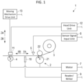
- FIG. 1 schematically shows an RFID tag issuing device 1 according to an embodiment.
- FIG. 2 schematically shows a block diagram of the RFID tag issuing device 1.
- a height direction is indicated by arrow ZA and arrow ZB.
- a conveyance direction is indicated by arrow XA and arrow XB.
- the conveyance direction intersects the height directions and may be perpendicular or substantially perpendicular thereto.
- An intersecting direction (e.g., the directions into and out of the page of FIG. 1 ) that is intersecting both the height direction and the conveyance direction is also defined.
- the intersecting direction may be perpendicular or substantially perpendicular to the height direction and the conveyance direction.
- the "carry-in side" along the conveyance direction corresponds to the pointing direction indicated by the arrow XA
- the "carry-out side” along the conveyance direction corresponds to the pointing direction indicated by the arrow XB.
- FIG. 3 shows a label sheet 3 that can be used in the RFID tag issuing device 1.
- a longitudinal direction indicated by arrow XC and arrow XD and a lateral direction indicated by arrow YC and arrow YD intersecting the longitudinal direction are defined.
- the lateral direction may be perpendicular or substantially perpendicular to the longitudinal direction.
- the label sheet 3 is used in the RFID tag issuing device 1 in a state in which the longitudinal direction of the label sheet 3 coincides with the conveyance direction within the RFID tag issuing device 1 and the lateral direction of the label sheet 3 coincides with the intersecting direction within the RFID tag issuing device 1.
- the RFID tag issuing device 1 includes conveyance rollers 2, a platen roller 4, a mark sensor 5, a sensor signal input unit 6, a motor 7, a motor drive unit 8, a reader/writer 9, an antenna 10, a print head 11, a head drive unit 12, a moving mechanism drive unit 13, a notification unit 14, an input unit 15, a communication interface (I/F) 16, a storage unit 17, and a processor 18.
- the label sheet 3 includes a plurality of labels 31, a strip-shaped mount 32 to which the plurality of labels 31 are attached, RFID tags 33, and marks 34.
- the label sheet 3 is, for example, a rolled sheet formed by winding the mount 32 on which the plurality of labels 31 are attached.
- the conveyance rollers 2 include, for example, a pair of rollers 21 and 22.
- the conveyance rollers 2 convey the rolled label sheet 3 along the conveyance path.
- the plurality of conveyance rollers 2 may be disposed on the conveyance path.
- the roller 21 is rotationally driven by the motor 7, and the roller 22 is rotated by the power of the rotational drive of the roller 21. That is, in this example, the roller 22 is a driven roller.
- the platen roller 4 rotates to convey the label sheet 3 along the conveyance path to the carry-out side along the conveyance direction.
- the platen roller 4 is disposed on the carry-out side of the conveyance roller 2 and the mark sensor 5 along the conveyance path.
- the platen roller 4 is rotationally driven by the motor 7.
- the mark sensor 5 is provided so as to face the conveyance path in the height direction.
- the mark sensor 5 is arranged on the carry-out side along the conveyance direction from the conveyance rollers 2 and on the carry-in side along the conveyance direction from the platen roller 4 on the conveyance path.
- the mark sensor 5 optically detects a mark on the label sheet 3.
- the mark sensor 5 scans the surface of the label sheet 3 conveyed along the conveyance direction to detect the mark on the mount 32.
- the mark sensor 5 outputs a signal to the sensor signal input unit 6.
- the sensor signal input unit 6 is connected to one or more sensors including the mark sensor 5.
- the sensor signal input unit 6 receives the signal from the mark sensor 5 and outputs the signal to a processor.
- the sensors include an open/close sensor.
- the open/close sensor detects opening and closing of a member that is opened and closed when the label sheet 3 is replaced.
- Examples of the member to be opened and closed include a cover, a door, and a lid.
- the open/close sensor may be, for example, an optical sensor that is switched on and off in response to closing or opening of the member.
- the open/close sensor may be a mechanical switch that is switched on and off in response to closing or opening of the member.
- the motor 7 is mechanically connected to the conveyance rollers 2 and the platen roller 4.
- the motor 7 rotates the conveyance rollers 2 and the platen roller 4.
- the motor 7 rotates the roller 21 of the conveyance rollers 2 and the platen roller 4 in a direction indicated by an arrow A illustrated in FIG. 1 .
- the motor 7 conveys the label sheet 3 along the conveyance path.
- the motor drive unit 8 controls rotation of the motor 7.
- the motor drive unit 8 controls forward rotation and reverse rotation of the motor 7.
- the motor drive unit 8 controls the motor 7 in a forward rotation state.
- the conveyance rollers 2 and the platen roller 4 rotate in the direction indicated by the arrow A in FIG. 1 , thereby conveying the label sheet 3 to the carry-out side in the conveyance direction.
- the reader/writer 9 communicates with the RFID tag 33 disposed on the label sheet 3 via the antenna 10 to write data to the RFID tag 33 and read data from the RFID tag 33.
- the reader/writer 9 emits radio waves for communicating with the RFID tag 33 from the antenna 10.
- the RFID tag 33 is activated by receiving the radio wave from the reader/writer 9, and transmits a response wave to the antenna 10.
- the reader/writer 9 receives the response wave from the RFID tag 33 by the antenna 10 and communicates with the RFID tag 33.
- the reader/writer 9 transmits an inquiry wave that is a modulated wave following a non-modulated wave to the RFID tag 33.
- the RFID tag 33 is activated by the non-modulated wave, and responds to the inquiry wave from the reader/writer 9. Also in response, the reader/writer 9 transmits a non-modulated wave to the RFID tag 33.
- the RFID tag 33 responds by reflecting the non-modulated wave from the reader/writer 9.
- the print head 11 is disposed so as to face the platen roller 4 in the height direction.
- the print head 11 is connected to the head drive unit 12.
- the print head 11 performs printing on a print surface of the conveyed label 31. That is, the print head 11 performs printing on the surface opposite to the surface on which the RFID tag 33 is provided.
- the head drive unit 12 drives the print head 11 to perform printing on the print surface of the label 31.
- the moving mechanism drive unit 13 reciprocates the print head 11 while the print head 11 is adjacent to the label sheet 3 being conveyed along the conveyance path.
- the notification unit 14 performs notification by screen display, sound emission, lighting, or the like. For example, information that needs to be recognized by a user, warning information to the user, and the like are notified by the notification unit 14.
- the notification unit 14 is, for example, a display.
- the input unit 15 includes an operation member. A command related to an operation of the RFID tag issuing device 1 is input by the user via the operation member. Examples of the operation member include a button, a dial, and a touch panel.
- the communication interface 16 is an interface connected to a host device. The communication interface 16 receives data to be written to an RFID tag 33, print data to be printed on a label 31, and the like from a host device. The communication interface 16 transmits data such as issuance result data to the host device.
- the storage unit 17 stores programs necessary for controlling the RFID tag issuing device 1 and various data such as print data and issuance result data.
- the storage unit 17 is, for example, a ROM (Read Only Memory), a RAM (Random Access Memory), an SSD (Solid State Drive) or the like.
- the processor 18 is, for example, a CPU (Central Processing Unit).
- the processor 18 is connected to the sensor signal input unit 6, the motor drive unit 8, the reader/writer 9, the head drive unit 12, the moving mechanism drive unit 13, the notification unit 14, the input unit 15, the communication interface 16, and the storage unit 17.
- the processor 18 controls each component based on the signal input from the sensor signal input unit 6 and the programs stored in the storage unit 17.
- the processor 18 executes the functions of the RFID tag issuing device 1.
- the processor 18 cooperates with the reader/writer 9 to read data from the RFID tag 33 or write data to the RFID tag 33 by the antenna 10.
- the plurality of labels 31 have a rectangular sheet shape.
- the labels 31 are attached to one of the main surfaces of the mount 32.
- Each of the labels 31 is arranged at intervals in the longitudinal direction.
- Each label 31 includes an adhesive surface on a surface facing the mount 32.
- the RFID tag 33 is provided on the adhesive surface of the label 31.
- the RFID tag 33 includes a film 35, a tag antenna 36, and an IC chip 37.
- the tag antenna 36 includes, for example, a matching circuit.
- the tag antenna 36 and the IC chip 37 are disposed on the film 35.
- each RFID tag 33 is a passive tag having no battery.
- Each of the marks 34 indicates the top position of the label 31 in the longitudinal direction of the label sheet 3. In one example, the length of the mark 34 in the longitudinal direction is shorter than the length of the gap between the adjacent labels 31. The position where the RFID tag 33 is attached to the label 31 is appropriately set depending on the type of the label sheet 3.
- the RFID tag 33 is disposed on the label 31 such that the tag antenna 36 of the RFID tag 33 intersects the longitudinal direction. In one example, the tag antenna 36 is disposed parallel or substantially parallel to the lateral direction.
- a length direction indicated by an arrow YE and an arrow VF, a width direction indicated by an arrow XE and an arrow XF intersecting or substantially perpendicular to the length direction, and a thickness direction indicated by an arrow ZE and an arrow ZF intersecting or substantially perpendicular to both the length direction and the width direction are defined.
- the antenna 10 can be disposed in the RFID tag issuing device 1 such that the length direction of the antenna 10 matches (or substantially matches) the intersecting direction of the RFID tag issuing device 1.
- the antenna 10 can be arranged in the RFID tag issuing device 1 such that the width direction of the antenna 10 matches (or substantially matches) the conveyance direction within the RFID tag issuing device 1.
- the antenna 10 can be arranged in the RFID tag issuing device 1 such that the thickness direction of the antenna 10 matches (or substantially matches) the height direction of the RFID tag issuing device 1.
- the antenna 10 is disposed away from the conveyance path in the height direction of the RFID tag issuing device 1.
- the distance by which the antenna 10 is separated from the conveyance path is appropriately set according to the radiation intensity of the antenna 10.
- the antenna 10 is separated from the conveyance path by 5 mm.
- the center of the antenna 10 in the width direction is arranged so as to coincide with or substantially coincide with the center of the conveyance path in the intersecting direction of the RFID tag issuing device 1. Therefore, the RFID tag 33 passes through the center side in the width direction of the antenna 10 by being conveyed along the conveyance path.
- the antenna 10 includes a dielectric substrate 101, a power supply point 102, a termination resistor 103, lines 104 and 105, and a ground layer 106.
- the dielectric substrate 101 is formed of a dielectric material.
- the dielectric substrate 101 has a rectangular plate shape.
- the dimension of the dielectric substrate 101 in the length direction is larger than the dimension thereof in the width direction.
- the dimensions of the dielectric substrate 101 in the length direction and the width direction are not limited thereto.
- the dimensions of the dielectric substrate 101 can be appropriately set in accordance with the mode of use or the like in the RFID tag issuing device 1.
- Via holes 107 penetrating the dielectric substrate 101 are formed in the dielectric substrate 101 in the thickness direction. As shown in FIG. 6 , the via holes 107 penetrate the dielectric substrate 101 from a first main surface 108 of the dielectric substrate 101 to a second main surface 109 of the dielectric substrate 101 in the thickness direction.
- the power supply point 102 is provided on one end side indicated by an arrow YF in the length direction.
- the power supply point 102 is connected to a first end portion 110 of extended portions of the lines 104 and 105.
- the termination resistor 103 is provided on an end portion side indicated by an arrow YE opposite to the end portion side on which the power supply point 102 is located in the length direction.
- the termination resistor 103 is connected to a second end portion 111 on the opposite side to the first end portion 110 formed by the lines 104 and 105.
- the lines 104 and 105 extend between the power supply point 102 and the termination resistor 103 in the length direction.
- the lines 104 and 105 are conductive connecting elements, which may also be referred to as wiring, wiring connections, wiring lines, electrical pathways, or the like.
- the resistance value of the termination resistor 103 is equal to a resistance value matching the characteristic impedance of the entire extended portion formed by the lines 104 and 105.
- both the power supply point 102 and the termination resistor 103 are disposed on one end side indicated by the arrow XF in the width direction. Both the power supply point 102 and the termination resistor 103 are disposed on the second surface 109 of the dielectric substrate 101.
- the positions of the power supply point 102 and the termination resistor 103 in the width direction are not limited to those described above, and they can be arranged as appropriate in accordance with the usage pattern or the like.
- the power supply point 102 and the termination resistor 103 may be disposed on the first surface 108 of the dielectric substrate 101.
- one of the power supply point 102 or the termination resistor 103 may be disposed on the first surface 108 of the dielectric substrate 101, and the other may be disposed on the second surface 109 of the dielectric substrate 101.
- the line 104 is formed on the first surface 108 of the dielectric substrate 101 (see FIG. 6 ) .
- the line 104 includes a plurality of loop portions (e.g., loop portions 1041, 1042, 1043, 1044) .
- Each of the loop portions 1041 to 1044 is adjacent to at least one other of the loop portions 1041 to 1044. That is, each of the loop portions 1041 to 1044 is close to at least one of the other loop portions 1041 to 1044, though some of the plurality of loop portions may be adjacent to two other loop portions.
- the loop portions 1041 to 1044 are not in contact with each other on the first surface 108 of the dielectric substrate 101.
- the loop portions 1041 to 1044 are arranged side by side with respect to each other in the length direction of the dielectric substrate 101.
- the loop portions 1041 to 1044 are arranged linearly or substantially linearly in the length direction.
- Vias 112 are formed at both ends of each of the loop portions 1041 to 1044.
- the via holes 107 of the dielectric substrate 101 shown in FIG. 6 are formed corresponding to the positions where the vias 112 are formed shown in FIG. 4 .
- the line 104 is electrically connected to the line 105 through the vias 112 in the via holes 107.
- each of the plurality of loop portions 1041 to 1044 is bent at three positions. That is, each of the plurality of loop portions 1041 to 1044 has two portions extending along the length direction of the dielectric substrate 101 and two portions extending along the width direction of the dielectric substrate 101. Specifically, each of the loop portions 1041 to 1044 extends along the length direction from one end portion, and then is bent towards and extends along the width direction. Further, each of the loop portions 1041 to 1044 is bent towards and extends towards the length direction, and then is bent towards the width direction and extends to the other end portion. Thus, each of the loop portions 1041 to 1044 forms a loop shape.
- the shape of the loop portions 1041 to 1044 is not limited to the shape described above. That is, as long as each of the loop portions 1041 to 1044 forms a loop shape, the loop shape can be appropriately adjusted in consideration of the size of the antenna 10, the required magnetic field, and the like.
- the four loop portions 1041 to 1044 are formed on the first surface 108 of the dielectric substrate 101, but the embodiments are not limited thereto. That is, in the antenna 10, the number of loop portions can be adjusted in consideration of the required magnetic field intensity and the like.
- the size of the loop portions 1041 to 1044 can be appropriately set according to the size of the antenna 10 or the like. However, when the size of each of the loop portions 1041 to 1044 is relatively large, the magnetic field generated by each of the loop portions 1041 to 1044 does not become overall strong inside each of the loop portions 1041 to 1044. That is, the intensity of the magnetic field is high at the edge portion of each of the loop portions 1041 to 1044, and the intensity of the magnetic field is low at the inner portion of each of the loop portions 1041 to 1044. Therefore, it is preferable that the size of each of the loop portions 1041 to 1044 is set such that the magnetic field generated by each of the loop portions 1041 to 1044 will be strong inside each of the loop portions 1041 to 1044.
- the line 105 is formed on the second surface 109 of the dielectric substrate 101.
- the line 105 includes a plurality of relay portions (e.g., relay portions 1051, 1052, 1053, 1054, 1055) .
- Each of the relay portions 1051 to 1055 is separated from the others in the length direction. That is, the relay portions 1051 to 1055 are not in contact with each other on the second surface 109 of the dielectric substrate 101.
- the relay portions 1051 to 1055 are arranged side by side with respect to each other in the length direction.
- Vias 113 are formed at both ends of each relay portion 1051 to 1055.
- the via holes 107 of the dielectric substrate 101 are formed corresponding to the positions where the vias 113 are formed.
- the line 105 is connected to the line 104 by the vias 113 and the via holes 107.
- the relay portion 1051 is disposed on the power supply point 102 side in the length direction and extends from one end portion along the width direction. In an embodiment, one end portion of the relay portion 1051 is connected to the power supply point 102.
- Each of the relay portions 1052 to 1054 extends along the length direction from one end portion, and is bent towards the width direction and extends along the width direction to the other end portion. That is, each of the relay portions 1052 to 1054 is formed in an L shape or a substantially L shape.
- the relay portion 1055 extends from one end portion along the width direction, and is bent towards the length direction. Further, the relay portion 1055 is bent towards the width direction and extended along the width direction to the other end portion. That is, the relay portion 1055 is formed in a U shape or a substantially U shape. In an embodiment, the other end portion of the relay portion 1055 is connected to the termination resistor 103.
- the relay portions 1052 to 1055 are respectively provided at portions of the second surface 109 corresponding to the positions of the loop portions 1041 to 1044 on the first surface 108.
- at least some of relay portions 1052 to 1055 is overlapping with loop portions 1041 to 1044 in a projection view from the thickness direction.
- the power supply point 102 is connected to the first end portion 110 of the relay portion 1051.
- the other end portion of the relay portion 1051 is connected to one end portion of the loop portion 1041 via the corresponding via 113, via hole 107, and via 112.
- the end portion of the loop portion 1041 not connected to the relay portion 1051 is connected to one end portion of the relay portion 1052 through the corresponding via 112, via hole 107, and via 113.
- the relay portions 1052 to 1054 are connected to corresponding loop portions 1042 to 1044 via the corresponding vias 112 and 113 and via holes 107.
- the termination resistor 103 is connected to the second end portion 111 of the relay portion 1055 not connected to the loop portion 1044.
- the ground layer 106 is provided on the second surface 109 of the dielectric substrate 101. As shown in FIG. 5 , the ground layer 106 may have a rectangular shape. The ground layer 106 is provided so as to avoid a region around the line 105. That is, a gap is formed between the line 105 and the ground layer 106. When the power supply point 102 and the termination resistor 103 are disposed on the second surface 109 of the dielectric substrate 101, the ground layer 106 is provided so as to avoid the region around the power supply point 102 and the termination resistor 103. That is, gaps are formed between the ground layer 106 and the power supply point 102 and the termination resistor 103.
- the ground layer 106 is provided not only on the second surface 109 but also in a region around the power supply point 102 and the termination resistor 103 on the first surface 108.
- the size of the ground layer 106 in the length direction is equal to or greater than the maximum size of the extended portions of the lines 104 and 105 in the length direction of the antenna 10. In addition, it is equal to or smaller than the size of the dielectric substrate 101 in the length direction.
- the size of the ground layer 106 in the width direction is equal to or larger than the maximum size of the extended portions of the lines 104 and 105 in the width direction of the antenna 10. In addition, it is equal to or less than the size of the dielectric substrate 101 in the width direction. In an embodiment, the size of the ground layer 106 in the length direction matches (or substantially matches) the size of the dielectric substrate 101 in the length direction.
- the size of the ground layer 106 in the width direction is equal or substantially equal to the size of the dielectric substrate 101 in the width direction.
- the size of the ground layer 106 is not limited to this.
- the ground layer 106 is preferably formed so as to cover the second surface 109 other than the portion where the power supply point 102, the termination resistor 103, and the line 105 are disposed.
- the lines 104 and 105 are provided between the power supply point 102 and the termination resistor 103, and each of the loop portions 1041 to 1044 is close to at least one of the other loop portions 1041 to 1044.
- magnetic fields generated by the loop portions 1041 to 1044 are generated to be close to each other in the length direction of the antenna 10. That is, the magnetic field generated by each of the loop portions 1041 to 1044 is not generated separated in the length direction of the antenna 10. Therefore, regions of high magnetic field intensity in the magnetic field generated by each of the loop portions 1041 to 1044 are formed in a concentrated state along the length direction of the antenna 10.
- the loop portions 1041 to 1044 are aligned in the length direction of the antenna 10.
- the magnetic field generated by the loop portions 1041 to 1044 is generated in a more concentrated state along the length direction of the antenna 10. Therefore, regions of high magnetic field intensity in the magnetic field generated by each of the loop portions 1041 to 1044 are formed in a more concentrated state in the length direction of the antenna 10.
- the ground layer 106 is preferably provided on the second main surface opposite to the first main surface on which the loop portions 1041 to 1044 are provided in the thickness direction.
- the ground layer 106 By disposing the ground layer 106 in this manner, it is possible to suppress generation of a magnetic field generated by the loop portions 1041 to 1044 in a direction from the first main surface 108 toward the second surface 109 in the thickness direction of the antenna 10. That is, in the antenna 10, the loop portions 1041 to 1044 generate a magnetic field in a direction from the second surface 109 toward the first surface 108. Thus, generation of a magnetic field in an unnecessary direction is suppressed in the antenna 10.
- the line 104 be disposed on the first surface 108, the line 105 be disposed on the second surface 109, and the line 104 and the line 105 to avoid overlap of each other as much as possible in a projection view from the thickness direction.
- the ground layer 106 preferably covers the second surface 109 as much as possible.
- the antenna 10 is disposed in the RFID tag issuing device 1 such that the length direction of the antenna 10 intersects with the conveyance direction within the RFID tag issuing device 1. That is, the magnetic field formed in parallel in the longitudinal direction of the antenna 10 is formed crossing while the label sheet 3 is being conveyed. Therefore, the RFID tag issuing device 1 can write data in the target RFID tag on the label sheet 3 regardless of the position of the label sheet 3 in the width direction of the antenna 10.
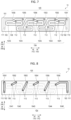
- FIGS. 7 and 8 are schematic antenna 10 according to a modification example.
- the length direction, the width direction, and the thickness direction are defined.
- the power supply point 102 is provided on one side in the length direction, and the termination resistor 103 is provided on the other side.
- the power supply point 102 is connected to the first end portion 110 of the extended portion formed by the lines 104 and 105.
- the termination resistor 103 is connected to the second end portion 111 of the extended portion formed by the lines 104 and 105.
- the lines 104 and 105 are connected to each other through corresponding vias 112 and 113 and via holes 107.
- the line 104 includes the loop portions 1041 to 1045, and the line 105 includes the relay portions 1051 to 1056.
- the loop portions 1041 to 1045 and the relay portions 1051 to 1056 are connected to each other through corresponding vias 112 and 113 and via holes 107.
- each of the loop portions 1041 to 1045 is bent at six positions, as illustrated in FIG. 7 . That is, each of the loop portions 1041 to 1045 has four portions extending along the length direction of the dielectric substrate 101 and three portions extending along the width direction of the dielectric substrate 101. In each of loop portions 1041 to 1045, one end portion is disposed on the point 102 side with respect to the other portion in the length direction of the dielectric substrate 101. In each of the loop portions 1041 to 1045, the pair of end portions are a shifted with respect to each other in the width direction.
- the loop portions 1041 to 1045 are shifted from the others in the width direction.
- at least some of the loop portions 1041 to 1045 are overlapping each other in projection view seen from the width direction. That is, the loop portions 1041 to 1045 are arranged in a staggered manner along the length direction on the first surface 108 of the dielectric substrate 101.
- the loop portions 1041, 1043, 1045 are provided on one side in the width direction and loop portions 1042 and 1044 are provided on the opposite side from loop portions 1041, 1043, and 1045 in the width direction.
- the loop portion 1042 has a portion overlapping with the loop portions 1041 and 1043 in a projection view from the width direction, and is between the loop portion 1041 and the loop portion 1043 in the length direction.
- the loop portion 1044 has a portion overlapping the loop portions 1043 and 1045 in a projection view from the width direction, and is between the loop portion 1043 and the loop portion 1045 in the length direction.
- the antenna 10 configured as described above, in the antenna 10 of the present modification example, a region in which the intensity of the magnetic field in the generated magnetic field is high is formed without interruption in the length direction. Therefore, the magnetic field can be generated in a continuous state in the length direction and in a further concentrated state. Also, the lines 104 and 105 are provided between the power supply point 102 and the termination resistor 103, and each of the loop portions 1041 to 1045 is close to at least one of the other loop portions 1041 to 1045. Therefore, the antenna 10 also exhibits the same effect as those of the above-described embodiments and the like. Therefore, in the RFID tag issuing device 1 using the antenna 10, even if the label sheet 3 is displaced to some extent in the direction intersecting the conveyance direction, it is possible to reliably write information in the target RFID tag.
Landscapes
- Engineering & Computer Science (AREA)
- Physics & Mathematics (AREA)
- Health & Medical Sciences (AREA)
- Toxicology (AREA)
- Computer Networks & Wireless Communication (AREA)
- Theoretical Computer Science (AREA)
- General Physics & Mathematics (AREA)
- Computer Vision & Pattern Recognition (AREA)
- Artificial Intelligence (AREA)
- General Health & Medical Sciences (AREA)
- Electromagnetism (AREA)
- General Engineering & Computer Science (AREA)
- Computer Hardware Design (AREA)
- Microelectronics & Electronic Packaging (AREA)
- Details Of Aerials (AREA)
- Variable-Direction Aerials And Aerial Arrays (AREA)
- Waveguide Aerials (AREA)
Claims (15)
- Antenne (10), comprenant :un point d'alimentation électrique (102) sur un substrat (101) ;une résistance (103) de terminaison sur le substrat (101) ;des première et deuxième lignes (104, 105) connectant le point d'alimentation électrique (102) et la résistance (103) de terminaison, la première ligne (104) se trouvant sur une première surface (108) du substrat (101), et la deuxième ligne (105) se trouvant sur une deuxième surface (109) du substrat (101), dans laquelle la première ligne (104) inclut une pluralité de portions formant boucle (1041-1044) espacées les unes des autres le long d'une direction longitudinale du substrat (101), et la deuxième ligne (105) inclut une pluralité de portions conductrices (1051-1055) connectant le point d'alimentation électrique (102) à l'une des portions formant boucle la plus proche de celui-ci, connectant des paires adjacentes de portions formant boucle les unes aux autres, et connectant la résistance (103) de terminaison à l'une des portions formant boucle la plus proche de celle-ci ;caractérisée en ce que la deuxième surface (109) du substrat (101) est opposée à la première surface (108) du substrat (101).
- Antenne (10) selon la revendication 1, dans laquelle chacune des portions formant boucle (1041-1044) inclut :une première partie s'étendant le long de la direction longitudinale,une deuxième partie connectée à la première partie et s'étendant le long d'une direction de largeur croisant la direction longitudinale,une troisième partie connectée à la deuxième partie et s'étendant le long de la direction longitudinale, etune quatrième partie connectée à la troisième partie et s'étendant le long de la direction de largeur vers la première partie.
- Antenne (10) selon la revendication 2, dans laquelle une extrémité de la quatrième partie de l'une des portions formant boucle (1044) est connectée à l'une des portions conductrices.
- Antenne (10) selon la revendication 3, dans laquelle une extrémité de la première partie de ladite une des portions formant boucle (1041) est connectée à l'une des portions conductrices (1051) directement connectées au point d'alimentation électrique (102).
- Antenne (10) selon l'une quelconque des revendications 2 à 4, dans laquelle une extrémité de la quatrième partie de l'une des portions formant boucle est connectée à l'une des portions conductrices directement connectées à la résistance (103) de terminaison.
- Antenne (10) selon l'une quelconque des revendications 1 à 5, dans laquelle le point d'alimentation électrique (102) et la résistance (103) de terminaison se trouvent sur la deuxième surface (109).
- Antenne (10) selon la revendication 6, dans laquelle la portion conductrice connectant le point d'alimentation électrique (102) et la une des portions formant boucles la plus proche de celui-ci s'étend le long d'une direction de largeur du substrat (101) croisant la direction longitudinale.
- Antenne (10) selon la revendication 6 ou la revendication 7, dans laquelle la portion conductrice connectant chaque paire adjacente des portions formant boucle présente une forme de L.
- Antenne (10) selon l'une quelconque des revendications 6 à 8, dans laquelle la portion conductrice connectant la résistance (103) de terminaison et la une des portions formant boucle la plus proche de celle-ci présente une forme de L.
- Antenne (10) selon l'une quelconque des revendications 1 à 7, dans laquellechacune des portions formant boucle (1041-1044) inclut une partie droite et une partie en forme de boucle, etles portions formant boucle (1041-1044) sont agencées de telle sorte que la partie en forme de boucle de chacune des portions formant boucle (1041-1044) est située en quinconce le long de la direction longitudinale.
- Antenne (10) selon la revendication 10, dans laquelle des parties en forme de boucle de deux des portions formant boucle se chevauchent partiellement lorsqu'on les voit depuis une direction de largeur du substrat (101) croisant la direction longitudinale.
- Dispositif (1) de traitement d'étiquette sans fil, comprenant :une antenne (10) selon la revendication 1 ; etun processeur (18) configuré pour amener l'antenne (10) à transmettre une onde radio de façon à écrire des informations dans une étiquette sans fil.
- Dispositif (1) de traitement d'étiquette sans fil selon la revendication 12, comprenant en outre :
un rouleau (2) d'acheminement configuré pour acheminer une étiquette à laquelle une étiquette sans fil est fixée le long d'une direction d'acheminement qui croise la direction longitudinale du substrat. - Dispositif (1) de traitement d'étiquette sans fil selon la revendication 13, comprenant en outre :un capteur configuré pour détecter une position de l'étiquette, dans lequelle processeur (18) est configuré pour commander la transmission de l'onde radio sur la base d'une sortie provenant du capteur.
- Dispositif (1) de traitement d'étiquette sans fil selon la revendication 13 ou revendication 14, comprenant en outre :
une tête (11) d'impression disposée sur un côté aval de l'antenne (10) dans la direction d'acheminement et configurée pour imprimer une image sur l'étiquette.
Applications Claiming Priority (1)
| Application Number | Priority Date | Filing Date | Title |
|---|---|---|---|
| JP2020195307A JP2022083778A (ja) | 2020-11-25 | 2020-11-25 | アンテナ及びrfidタグ発行装置 |
Publications (2)
| Publication Number | Publication Date |
|---|---|
| EP4006779A1 EP4006779A1 (fr) | 2022-06-01 |
| EP4006779B1 true EP4006779B1 (fr) | 2023-08-16 |
Family
ID=76845062
Family Applications (1)
| Application Number | Title | Priority Date | Filing Date |
|---|---|---|---|
| EP21184473.3A Active EP4006779B1 (fr) | 2020-11-25 | 2021-07-08 | Antenne et dispositif de traitement d'étiquette sans fil |
Country Status (4)
| Country | Link |
|---|---|
| US (1) | US11544482B2 (fr) |
| EP (1) | EP4006779B1 (fr) |
| JP (1) | JP2022083778A (fr) |
| CN (1) | CN114552164A (fr) |
Family Cites Families (10)
| Publication number | Priority date | Publication date | Assignee | Title |
|---|---|---|---|---|
| JPH10209737A (ja) | 1996-11-22 | 1998-08-07 | Teruya:Kk | ループアンテナおよび認証装置 |
| JP2005182637A (ja) | 2003-12-22 | 2005-07-07 | Shinko Electric Ind Co Ltd | Icタグのrw用アンテナ |
| JP3935162B2 (ja) | 2004-04-28 | 2007-06-20 | 東芝テック株式会社 | Rfタグリーダ/ライタおよびプリンタ |
| US7832952B2 (en) | 2007-03-21 | 2010-11-16 | Avery Dennison Corporation | High-frequency RFID printer |
| US8254833B2 (en) * | 2009-05-11 | 2012-08-28 | Zih Corp. | Near field coupling devices and associated systems and methods |
| US8878652B2 (en) | 2009-11-13 | 2014-11-04 | Zih Corp. | Encoding module, associated encoding element, connector, printer-encoder and access control system |
| JP5629655B2 (ja) | 2011-07-12 | 2014-11-26 | 東芝テック株式会社 | Rfidタグ発行装置及びrfidタグの位置ずれ検出方法 |
| JP6392715B2 (ja) | 2015-08-17 | 2018-09-19 | 日本電信電話株式会社 | ループアンテナアレイ群 |
| JP7391578B2 (ja) | 2019-09-06 | 2023-12-05 | 東芝テック株式会社 | アンテナ及びrfidタグ発行装置 |
| US11392783B2 (en) * | 2020-03-12 | 2022-07-19 | KYOCERA AVX Components (San Diego), Inc. | RFID printer-encoder having a multi-mode active antenna |
-
2020
- 2020-11-25 JP JP2020195307A patent/JP2022083778A/ja active Pending
-
2021
- 2021-05-14 CN CN202110526488.1A patent/CN114552164A/zh active Pending
- 2021-05-24 US US17/329,051 patent/US11544482B2/en active Active
- 2021-07-08 EP EP21184473.3A patent/EP4006779B1/fr active Active
Also Published As
| Publication number | Publication date |
|---|---|
| JP2022083778A (ja) | 2022-06-06 |
| US20220164555A1 (en) | 2022-05-26 |
| CN114552164A (zh) | 2022-05-27 |
| EP4006779A1 (fr) | 2022-06-01 |
| US11544482B2 (en) | 2023-01-03 |
Similar Documents
| Publication | Publication Date | Title |
|---|---|---|
| KR101455220B1 (ko) | 인코딩 모듈, 관련 인코딩 요소, 컨넥터, 프린터-인코더, 및 액세스 제어 시스템 | |
| EP1943611B1 (fr) | procédé pour le réglage d'un coupleur à champ proche | |
| US7398054B2 (en) | Spatially selective UHF near field microstrip coupler device and RFID systems using device | |
| US20050280537A1 (en) | RFID printer and antennas | |
| US8258929B2 (en) | Encoding a RFID record member on a moving web | |
| US20100039235A1 (en) | Antenna device and apparatus for communicating with RFID tag | |
| WO2010132417A1 (fr) | Dispositif de couplage en champ proche et système et procédé associés | |
| US8068032B2 (en) | Apparatus for communicating with a RFID tag | |
| US11993072B2 (en) | Printer and wireless tag writing device | |
| CN112467358B (zh) | 天线及rfid标签发放装置 | |
| EP4006779B1 (fr) | Antenne et dispositif de traitement d'étiquette sans fil | |
| CN110119791B (zh) | 标签发放装置 | |
| JP2012103942A (ja) | Icタグ通信装置 |
Legal Events
| Date | Code | Title | Description |
|---|---|---|---|
| PUAI | Public reference made under article 153(3) epc to a published international application that has entered the european phase |
Free format text: ORIGINAL CODE: 0009012 |
|
| STAA | Information on the status of an ep patent application or granted ep patent |
Free format text: STATUS: THE APPLICATION HAS BEEN PUBLISHED |
|
| AK | Designated contracting states |
Kind code of ref document: A1 Designated state(s): AL AT BE BG CH CY CZ DE DK EE ES FI FR GB GR HR HU IE IS IT LI LT LU LV MC MK MT NL NO PL PT RO RS SE SI SK SM TR |
|
| STAA | Information on the status of an ep patent application or granted ep patent |
Free format text: STATUS: REQUEST FOR EXAMINATION WAS MADE |
|
| 17P | Request for examination filed |
Effective date: 20221103 |
|
| RBV | Designated contracting states (corrected) |
Designated state(s): AL AT BE BG CH CY CZ DE DK EE ES FI FR GB GR HR HU IE IS IT LI LT LU LV MC MK MT NL NO PL PT RO RS SE SI SK SM TR |
|
| GRAP | Despatch of communication of intention to grant a patent |
Free format text: ORIGINAL CODE: EPIDOSNIGR1 |
|
| STAA | Information on the status of an ep patent application or granted ep patent |
Free format text: STATUS: GRANT OF PATENT IS INTENDED |
|
| RIC1 | Information provided on ipc code assigned before grant |
Ipc: H01Q 7/00 20060101ALI20230222BHEP Ipc: G06K 7/10 20060101ALI20230222BHEP Ipc: H01Q 1/22 20060101ALI20230222BHEP Ipc: G06K 17/00 20060101AFI20230222BHEP |
|
| INTG | Intention to grant announced |
Effective date: 20230315 |
|
| GRAS | Grant fee paid |
Free format text: ORIGINAL CODE: EPIDOSNIGR3 |
|
| GRAA | (expected) grant |
Free format text: ORIGINAL CODE: 0009210 |
|
| STAA | Information on the status of an ep patent application or granted ep patent |
Free format text: STATUS: THE PATENT HAS BEEN GRANTED |
|
| AK | Designated contracting states |
Kind code of ref document: B1 Designated state(s): AL AT BE BG CH CY CZ DE DK EE ES FI FR GB GR HR HU IE IS IT LI LT LU LV MC MK MT NL NO PL PT RO RS SE SI SK SM TR |
|
| REG | Reference to a national code |
Ref country code: CH Ref legal event code: EP Ref country code: DE Ref legal event code: R096 Ref document number: 602021004284 Country of ref document: DE |
|
| REG | Reference to a national code |
Ref country code: IE Ref legal event code: FG4D |
|
| REG | Reference to a national code |
Ref country code: LT Ref legal event code: MG9D |
|
| REG | Reference to a national code |
Ref country code: NL Ref legal event code: MP Effective date: 20230816 |
|
| REG | Reference to a national code |
Ref country code: AT Ref legal event code: MK05 Ref document number: 1600785 Country of ref document: AT Kind code of ref document: T Effective date: 20230816 |
|
| PG25 | Lapsed in a contracting state [announced via postgrant information from national office to epo] |
Ref country code: GR Free format text: LAPSE BECAUSE OF FAILURE TO SUBMIT A TRANSLATION OF THE DESCRIPTION OR TO PAY THE FEE WITHIN THE PRESCRIBED TIME-LIMIT Effective date: 20231117 |
|
| PG25 | Lapsed in a contracting state [announced via postgrant information from national office to epo] |
Ref country code: IS Free format text: LAPSE BECAUSE OF FAILURE TO SUBMIT A TRANSLATION OF THE DESCRIPTION OR TO PAY THE FEE WITHIN THE PRESCRIBED TIME-LIMIT Effective date: 20231216 |
|
| PG25 | Lapsed in a contracting state [announced via postgrant information from national office to epo] |
Ref country code: SE Free format text: LAPSE BECAUSE OF FAILURE TO SUBMIT A TRANSLATION OF THE DESCRIPTION OR TO PAY THE FEE WITHIN THE PRESCRIBED TIME-LIMIT Effective date: 20230816 Ref country code: RS Free format text: LAPSE BECAUSE OF FAILURE TO SUBMIT A TRANSLATION OF THE DESCRIPTION OR TO PAY THE FEE WITHIN THE PRESCRIBED TIME-LIMIT Effective date: 20230816 Ref country code: PT Free format text: LAPSE BECAUSE OF FAILURE TO SUBMIT A TRANSLATION OF THE DESCRIPTION OR TO PAY THE FEE WITHIN THE PRESCRIBED TIME-LIMIT Effective date: 20231218 Ref country code: NO Free format text: LAPSE BECAUSE OF FAILURE TO SUBMIT A TRANSLATION OF THE DESCRIPTION OR TO PAY THE FEE WITHIN THE PRESCRIBED TIME-LIMIT Effective date: 20231116 Ref country code: NL Free format text: LAPSE BECAUSE OF FAILURE TO SUBMIT A TRANSLATION OF THE DESCRIPTION OR TO PAY THE FEE WITHIN THE PRESCRIBED TIME-LIMIT Effective date: 20230816 Ref country code: LV Free format text: LAPSE BECAUSE OF FAILURE TO SUBMIT A TRANSLATION OF THE DESCRIPTION OR TO PAY THE FEE WITHIN THE PRESCRIBED TIME-LIMIT Effective date: 20230816 Ref country code: LT Free format text: LAPSE BECAUSE OF FAILURE TO SUBMIT A TRANSLATION OF THE DESCRIPTION OR TO PAY THE FEE WITHIN THE PRESCRIBED TIME-LIMIT Effective date: 20230816 Ref country code: IS Free format text: LAPSE BECAUSE OF FAILURE TO SUBMIT A TRANSLATION OF THE DESCRIPTION OR TO PAY THE FEE WITHIN THE PRESCRIBED TIME-LIMIT Effective date: 20231216 Ref country code: HR Free format text: LAPSE BECAUSE OF FAILURE TO SUBMIT A TRANSLATION OF THE DESCRIPTION OR TO PAY THE FEE WITHIN THE PRESCRIBED TIME-LIMIT Effective date: 20230816 Ref country code: GR Free format text: LAPSE BECAUSE OF FAILURE TO SUBMIT A TRANSLATION OF THE DESCRIPTION OR TO PAY THE FEE WITHIN THE PRESCRIBED TIME-LIMIT Effective date: 20231117 Ref country code: FI Free format text: LAPSE BECAUSE OF FAILURE TO SUBMIT A TRANSLATION OF THE DESCRIPTION OR TO PAY THE FEE WITHIN THE PRESCRIBED TIME-LIMIT Effective date: 20230816 Ref country code: AT Free format text: LAPSE BECAUSE OF FAILURE TO SUBMIT A TRANSLATION OF THE DESCRIPTION OR TO PAY THE FEE WITHIN THE PRESCRIBED TIME-LIMIT Effective date: 20230816 |
|
| PG25 | Lapsed in a contracting state [announced via postgrant information from national office to epo] |
Ref country code: PL Free format text: LAPSE BECAUSE OF FAILURE TO SUBMIT A TRANSLATION OF THE DESCRIPTION OR TO PAY THE FEE WITHIN THE PRESCRIBED TIME-LIMIT Effective date: 20230816 |
|
| PG25 | Lapsed in a contracting state [announced via postgrant information from national office to epo] |
Ref country code: ES Free format text: LAPSE BECAUSE OF FAILURE TO SUBMIT A TRANSLATION OF THE DESCRIPTION OR TO PAY THE FEE WITHIN THE PRESCRIBED TIME-LIMIT Effective date: 20230816 |
|
| PG25 | Lapsed in a contracting state [announced via postgrant information from national office to epo] |
Ref country code: SM Free format text: LAPSE BECAUSE OF FAILURE TO SUBMIT A TRANSLATION OF THE DESCRIPTION OR TO PAY THE FEE WITHIN THE PRESCRIBED TIME-LIMIT Effective date: 20230816 Ref country code: RO Free format text: LAPSE BECAUSE OF FAILURE TO SUBMIT A TRANSLATION OF THE DESCRIPTION OR TO PAY THE FEE WITHIN THE PRESCRIBED TIME-LIMIT Effective date: 20230816 Ref country code: ES Free format text: LAPSE BECAUSE OF FAILURE TO SUBMIT A TRANSLATION OF THE DESCRIPTION OR TO PAY THE FEE WITHIN THE PRESCRIBED TIME-LIMIT Effective date: 20230816 Ref country code: EE Free format text: LAPSE BECAUSE OF FAILURE TO SUBMIT A TRANSLATION OF THE DESCRIPTION OR TO PAY THE FEE WITHIN THE PRESCRIBED TIME-LIMIT Effective date: 20230816 Ref country code: DK Free format text: LAPSE BECAUSE OF FAILURE TO SUBMIT A TRANSLATION OF THE DESCRIPTION OR TO PAY THE FEE WITHIN THE PRESCRIBED TIME-LIMIT Effective date: 20230816 Ref country code: CZ Free format text: LAPSE BECAUSE OF FAILURE TO SUBMIT A TRANSLATION OF THE DESCRIPTION OR TO PAY THE FEE WITHIN THE PRESCRIBED TIME-LIMIT Effective date: 20230816 Ref country code: SK Free format text: LAPSE BECAUSE OF FAILURE TO SUBMIT A TRANSLATION OF THE DESCRIPTION OR TO PAY THE FEE WITHIN THE PRESCRIBED TIME-LIMIT Effective date: 20230816 |
|
| REG | Reference to a national code |
Ref country code: DE Ref legal event code: R097 Ref document number: 602021004284 Country of ref document: DE |
|
| PLBE | No opposition filed within time limit |
Free format text: ORIGINAL CODE: 0009261 |
|
| STAA | Information on the status of an ep patent application or granted ep patent |
Free format text: STATUS: NO OPPOSITION FILED WITHIN TIME LIMIT |
|
| 26N | No opposition filed |
Effective date: 20240517 |
|
| PG25 | Lapsed in a contracting state [announced via postgrant information from national office to epo] |
Ref country code: IT Free format text: LAPSE BECAUSE OF FAILURE TO SUBMIT A TRANSLATION OF THE DESCRIPTION OR TO PAY THE FEE WITHIN THE PRESCRIBED TIME-LIMIT Effective date: 20230816 Ref country code: SI Free format text: LAPSE BECAUSE OF FAILURE TO SUBMIT A TRANSLATION OF THE DESCRIPTION OR TO PAY THE FEE WITHIN THE PRESCRIBED TIME-LIMIT Effective date: 20230816 |
|
| PGFP | Annual fee paid to national office [announced via postgrant information from national office to epo] |
Ref country code: FR Payment date: 20240524 Year of fee payment: 4 |