EP4005776A1 - Cured resin formation method and cured resin formation device - Google Patents
Cured resin formation method and cured resin formation device Download PDFInfo
- Publication number
- EP4005776A1 EP4005776A1 EP19939655.7A EP19939655A EP4005776A1 EP 4005776 A1 EP4005776 A1 EP 4005776A1 EP 19939655 A EP19939655 A EP 19939655A EP 4005776 A1 EP4005776 A1 EP 4005776A1
- Authority
- EP
- European Patent Office
- Prior art keywords
- curable resin
- ultraviolet curable
- ultraviolet
- resin
- temperature
- Prior art date
- Legal status (The legal status is an assumption and is not a legal conclusion. Google has not performed a legal analysis and makes no representation as to the accuracy of the status listed.)
- Granted
Links
Images





Classifications
-
- B—PERFORMING OPERATIONS; TRANSPORTING
- B29—WORKING OF PLASTICS; WORKING OF SUBSTANCES IN A PLASTIC STATE IN GENERAL
- B29C—SHAPING OR JOINING OF PLASTICS; SHAPING OF MATERIAL IN A PLASTIC STATE, NOT OTHERWISE PROVIDED FOR; AFTER-TREATMENT OF THE SHAPED PRODUCTS, e.g. REPAIRING
- B29C35/00—Heating, cooling or curing, e.g. crosslinking or vulcanising; Apparatus therefor
- B29C35/02—Heating or curing, e.g. crosslinking or vulcanizing during moulding, e.g. in a mould
- B29C35/08—Heating or curing, e.g. crosslinking or vulcanizing during moulding, e.g. in a mould by wave energy or particle radiation
- B29C35/0805—Heating or curing, e.g. crosslinking or vulcanizing during moulding, e.g. in a mould by wave energy or particle radiation using electromagnetic radiation
-
- C—CHEMISTRY; METALLURGY
- C08—ORGANIC MACROMOLECULAR COMPOUNDS; THEIR PREPARATION OR CHEMICAL WORKING-UP; COMPOSITIONS BASED THEREON
- C08F—MACROMOLECULAR COMPOUNDS OBTAINED BY REACTIONS ONLY INVOLVING CARBON-TO-CARBON UNSATURATED BONDS
- C08F2/00—Processes of polymerisation
- C08F2/46—Polymerisation initiated by wave energy or particle radiation
- C08F2/48—Polymerisation initiated by wave energy or particle radiation by ultraviolet or visible light
-
- B—PERFORMING OPERATIONS; TRANSPORTING
- B29—WORKING OF PLASTICS; WORKING OF SUBSTANCES IN A PLASTIC STATE IN GENERAL
- B29C—SHAPING OR JOINING OF PLASTICS; SHAPING OF MATERIAL IN A PLASTIC STATE, NOT OTHERWISE PROVIDED FOR; AFTER-TREATMENT OF THE SHAPED PRODUCTS, e.g. REPAIRING
- B29C35/00—Heating, cooling or curing, e.g. crosslinking or vulcanising; Apparatus therefor
- B29C35/16—Cooling
-
- B—PERFORMING OPERATIONS; TRANSPORTING
- B29—WORKING OF PLASTICS; WORKING OF SUBSTANCES IN A PLASTIC STATE IN GENERAL
- B29C—SHAPING OR JOINING OF PLASTICS; SHAPING OF MATERIAL IN A PLASTIC STATE, NOT OTHERWISE PROVIDED FOR; AFTER-TREATMENT OF THE SHAPED PRODUCTS, e.g. REPAIRING
- B29C64/00—Additive manufacturing, i.e. manufacturing of three-dimensional [3D] objects by additive deposition, additive agglomeration or additive layering, e.g. by 3D printing, stereolithography or selective laser sintering
- B29C64/30—Auxiliary operations or equipment
- B29C64/386—Data acquisition or data processing for additive manufacturing
- B29C64/393—Data acquisition or data processing for additive manufacturing for controlling or regulating additive manufacturing processes
-
- B—PERFORMING OPERATIONS; TRANSPORTING
- B33—ADDITIVE MANUFACTURING TECHNOLOGY
- B33Y—ADDITIVE MANUFACTURING, i.e. MANUFACTURING OF THREE-DIMENSIONAL [3D] OBJECTS BY ADDITIVE DEPOSITION, ADDITIVE AGGLOMERATION OR ADDITIVE LAYERING, e.g. BY 3D PRINTING, STEREOLITHOGRAPHY OR SELECTIVE LASER SINTERING
- B33Y30/00—Apparatus for additive manufacturing; Details thereof or accessories therefor
-
- B—PERFORMING OPERATIONS; TRANSPORTING
- B33—ADDITIVE MANUFACTURING TECHNOLOGY
- B33Y—ADDITIVE MANUFACTURING, i.e. MANUFACTURING OF THREE-DIMENSIONAL [3D] OBJECTS BY ADDITIVE DEPOSITION, ADDITIVE AGGLOMERATION OR ADDITIVE LAYERING, e.g. BY 3D PRINTING, STEREOLITHOGRAPHY OR SELECTIVE LASER SINTERING
- B33Y50/00—Data acquisition or data processing for additive manufacturing
- B33Y50/02—Data acquisition or data processing for additive manufacturing for controlling or regulating additive manufacturing processes
-
- H—ELECTRICITY
- H05—ELECTRIC TECHNIQUES NOT OTHERWISE PROVIDED FOR
- H05K—PRINTED CIRCUITS; CASINGS OR CONSTRUCTIONAL DETAILS OF ELECTRIC APPARATUS; MANUFACTURE OF ASSEMBLAGES OF ELECTRICAL COMPONENTS
- H05K3/00—Apparatus or processes for manufacturing printed circuits
- H05K3/46—Manufacturing multilayer circuits
- H05K3/4644—Manufacturing multilayer circuits by building the multilayer layer by layer, i.e. build-up multilayer circuits
- H05K3/4673—Application methods or materials of intermediate insulating layers not specially adapted to any one of the previous methods of adding a circuit layer
-
- B—PERFORMING OPERATIONS; TRANSPORTING
- B29—WORKING OF PLASTICS; WORKING OF SUBSTANCES IN A PLASTIC STATE IN GENERAL
- B29C—SHAPING OR JOINING OF PLASTICS; SHAPING OF MATERIAL IN A PLASTIC STATE, NOT OTHERWISE PROVIDED FOR; AFTER-TREATMENT OF THE SHAPED PRODUCTS, e.g. REPAIRING
- B29C35/00—Heating, cooling or curing, e.g. crosslinking or vulcanising; Apparatus therefor
- B29C35/02—Heating or curing, e.g. crosslinking or vulcanizing during moulding, e.g. in a mould
- B29C35/08—Heating or curing, e.g. crosslinking or vulcanizing during moulding, e.g. in a mould by wave energy or particle radiation
- B29C35/0805—Heating or curing, e.g. crosslinking or vulcanizing during moulding, e.g. in a mould by wave energy or particle radiation using electromagnetic radiation
- B29C2035/0827—Heating or curing, e.g. crosslinking or vulcanizing during moulding, e.g. in a mould by wave energy or particle radiation using electromagnetic radiation using UV radiation
-
- B—PERFORMING OPERATIONS; TRANSPORTING
- B29—WORKING OF PLASTICS; WORKING OF SUBSTANCES IN A PLASTIC STATE IN GENERAL
- B29C—SHAPING OR JOINING OF PLASTICS; SHAPING OF MATERIAL IN A PLASTIC STATE, NOT OTHERWISE PROVIDED FOR; AFTER-TREATMENT OF THE SHAPED PRODUCTS, e.g. REPAIRING
- B29C64/00—Additive manufacturing, i.e. manufacturing of three-dimensional [3D] objects by additive deposition, additive agglomeration or additive layering, e.g. by 3D printing, stereolithography or selective laser sintering
- B29C64/10—Processes of additive manufacturing
- B29C64/106—Processes of additive manufacturing using only liquids or viscous materials, e.g. depositing a continuous bead of viscous material
- B29C64/124—Processes of additive manufacturing using only liquids or viscous materials, e.g. depositing a continuous bead of viscous material using layers of liquid which are selectively solidified
-
- B—PERFORMING OPERATIONS; TRANSPORTING
- B33—ADDITIVE MANUFACTURING TECHNOLOGY
- B33Y—ADDITIVE MANUFACTURING, i.e. MANUFACTURING OF THREE-DIMENSIONAL [3D] OBJECTS BY ADDITIVE DEPOSITION, ADDITIVE AGGLOMERATION OR ADDITIVE LAYERING, e.g. BY 3D PRINTING, STEREOLITHOGRAPHY OR SELECTIVE LASER SINTERING
- B33Y10/00—Processes of additive manufacturing
-
- B—PERFORMING OPERATIONS; TRANSPORTING
- B33—ADDITIVE MANUFACTURING TECHNOLOGY
- B33Y—ADDITIVE MANUFACTURING, i.e. MANUFACTURING OF THREE-DIMENSIONAL [3D] OBJECTS BY ADDITIVE DEPOSITION, ADDITIVE AGGLOMERATION OR ADDITIVE LAYERING, e.g. BY 3D PRINTING, STEREOLITHOGRAPHY OR SELECTIVE LASER SINTERING
- B33Y80/00—Products made by additive manufacturing
-
- H—ELECTRICITY
- H05—ELECTRIC TECHNIQUES NOT OTHERWISE PROVIDED FOR
- H05K—PRINTED CIRCUITS; CASINGS OR CONSTRUCTIONAL DETAILS OF ELECTRIC APPARATUS; MANUFACTURE OF ASSEMBLAGES OF ELECTRICAL COMPONENTS
- H05K2203/00—Indexing scheme relating to apparatus or processes for manufacturing printed circuits covered by H05K3/00
- H05K2203/01—Tools for processing; Objects used during processing
- H05K2203/0104—Tools for processing; Objects used during processing for patterning or coating
- H05K2203/013—Inkjet printing, e.g. for printing insulating material or resist
-
- H—ELECTRICITY
- H05—ELECTRIC TECHNIQUES NOT OTHERWISE PROVIDED FOR
- H05K—PRINTED CIRCUITS; CASINGS OR CONSTRUCTIONAL DETAILS OF ELECTRIC APPARATUS; MANUFACTURE OF ASSEMBLAGES OF ELECTRICAL COMPONENTS
- H05K2203/00—Indexing scheme relating to apparatus or processes for manufacturing printed circuits covered by H05K3/00
- H05K2203/11—Treatments characterised by their effect, e.g. heating, cooling, roughening
- H05K2203/1121—Cooling, e.g. specific areas of a PCB being cooled during reflow soldering
-
- H—ELECTRICITY
- H05—ELECTRIC TECHNIQUES NOT OTHERWISE PROVIDED FOR
- H05K—PRINTED CIRCUITS; CASINGS OR CONSTRUCTIONAL DETAILS OF ELECTRIC APPARATUS; MANUFACTURE OF ASSEMBLAGES OF ELECTRICAL COMPONENTS
- H05K3/00—Apparatus or processes for manufacturing printed circuits
- H05K3/10—Apparatus or processes for manufacturing printed circuits in which conductive material is applied to the insulating support in such a manner as to form the desired conductive pattern
- H05K3/12—Apparatus or processes for manufacturing printed circuits in which conductive material is applied to the insulating support in such a manner as to form the desired conductive pattern using thick film techniques, e.g. printing techniques to apply the conductive material or similar techniques for applying conductive paste or ink patterns
- H05K3/1283—After-treatment of the printed patterns, e.g. sintering or curing methods
Definitions
- the present invention relates to a cured resin formation method and a cured resin formation device that cures an ultraviolet curable resin by irradiating the ultraviolet curable resin with ultraviolet rays.
- Patent Literature As described in the following Patent Literature, a technique for curing an ultraviolet curable resin to form a shaped object by irradiating the ultraviolet curable resin with ultraviolet rays has been developed.
- Patent Literature 1 JP-A-2013-67016
- the present specification discloses a cured resin formation method including an applying step of applying an ultraviolet curable resin on a base; and a curing step of curing the ultraviolet curable resin by irradiating the ultraviolet curable resin applied in the applying step with ultraviolet rays, in which in the curing step, the ultraviolet curable resin is irradiated with ultraviolet rays while cooling the ultraviolet curable resin, so that a difference between an ordinary temperature of the ultraviolet curable resin and a temperature of the ultraviolet curable resin when irradiated with ultraviolet rays is within a set temperature difference set in advance.
- the present specification discloses a cured resin formation device including an applying device configured to apply an ultraviolet curable resin on a base; and an irradiation device configured to cure the ultraviolet curable resin by irradiating the ultraviolet curable resin applied by the applying device with ultraviolet rays, in which the irradiation device irradiates the ultraviolet curable resin with ultraviolet rays while cooling the ultraviolet curable resin so that a difference between an ordinary temperature of the ultraviolet curable resin and a temperature of the ultraviolet curable resin when irradiated with ultraviolet rays is within a set temperature difference set in advance.
- the ultraviolet curable resin is irradiated with ultraviolet rays while the ultraviolet curable resin is cooled so that the difference between the ordinary temperature of the ultraviolet curable resin and the temperature of the ultraviolet curable resin when irradiated with ultraviolet rays is within the set temperature difference set in advance.
- the difference between the ordinary temperature of the ultraviolet curable resin and the temperature of the ultraviolet curable resin when irradiated with ultraviolet rays is within the set temperature difference set in advance.
- Fig. 1 illustrates circuit formation device 10.
- Circuit formation device 10 is provided with conveyance device 20, first shaping unit 22, second shaping unit 24, and control device 26 (refer to Fig. 2 ).
- Conveyance device 20, first shaping unit 22, and second shaping unit 24 are disposed on base 28 of circuit formation device 10.
- Base 28 has a substantially rectangular shape, and in the following description, the longitudinal direction of base 28 will be referred to as the X-axis direction, the shorter direction of base 28 will be referred to as the Y-axis direction, and the direction orthogonal to both the X-axis direction and the Y-axis direction will be referred to as the Z-axis direction.
- Conveyance device 20 is provided with X-axis slide mechanism 30 and Y-axis slide mechanism 32.
- X-axis slide mechanism 30 includes X-axis slide rail 34 and X-axis slider 36.
- X-axis slide rail 34 is disposed on base 28 so as to extend in the X-axis direction.
- X-axis slider 36 is held by X-axis slide rail 34 so as to be slidable in the X-axis direction.
- X-axis slide mechanism 30 includes electromagnetic motor (refer to Fig. 2 ) 38, and moves X-axis slider 36 to any position in the X-axis direction by driving electromagnetic motor 38.
- Y-axis slide mechanism 32 includes Y-axis slide rail 50 and stage 52.
- Y-axis slide rail 50 is disposed on base 28 so as to extend in the Y-axis direction and is movable in the X-axis direction.
- One end portion of Y-axis slide rail 50 is coupled to X-axis slider 36.
- Stage 52 is held on Y-axis slide rail 50 to be slidable in the Y-axis direction.
- Y-axis slide mechanism 32 includes electromagnetic motor (refer to Fig. 2 ) 56, and stage 52 moves to any position in the Y-axis direction by driving electromagnetic motor 56.
- stage 52 is moved to any position on base 28
- Stage 52 includes base plate 60, holding device 62, lifting and lowering device (refer to Fig. 2 ) 64, and cooling device 66.
- Base plate 60 is formed in a flat plate shape, and a board is placed on an upper surface of base plate 60.
- Holding devices 62 are provided on both side portions of base plate 60 in the X-axis direction.
- the board placed on base plate 60 is fixedly held by interposing both edge portions of the board in the X-axis direction with holding devices 62.
- lifting and lowering device 64 is disposed below base plate 60, and lifts and lowers base plate 60.
- cooling device 66 is disposed inside base plate 60 to cool base plate 60 to a predetermined temperature.
- First shaping unit 22 is a unit for shaping wiring on board 70 (refer to Fig. 3 ) placed on base plate 60 of stage 52, and includes first printing section 72 and drying section 74.
- First printing section 72 includes ink jet head 76 (refer to Fig. 2 ), and discharges metal ink linearly on board 70 placed on base plate 60.
- Metal ink is ink in which fine metal particles are dispersed in a solvent.
- Inkjet head 76 discharges a conductive material from multiple nozzles, for example, by a piezo method using a piezoelectric element.
- Drying section 74 includes ultraviolet irradiation device 78 (refer to Fig. 2 ).
- Ultraviolet irradiation device 78 is a device for irradiating the metal ink discharged on board 70 with ultraviolet rays, and the metal ink is dried by irradiating with ultraviolet rays. At this time, the solvent is vaporized by the drying of the metal ink, and the metal fine particles contact or aggregate with each other, and thus metal wiring is formed.
- second shaping unit 24 is a unit for shaping a resin layer on board 70 placed on base plate 60 of stage 52, and includes second printing section 84 and curing section 86.
- Second printing section 84 includes ink jet head 88 (refer to Fig. 2 ), and discharges the ultraviolet curable resin onto board 70 placed on base plate 60.
- Ink jet head 88 may be, for example, a piezo method using a piezoelectric element, or may be a thermal method in which a resin is heated to generate air bubbles and discharged from a nozzle.
- Curing section 86 includes flattening device (refer to Fig. 2 ) 90 and irradiation device (refer to Fig. 2 ) 92.
- Flattening device 90 is a device for flattening an upper surface of the ultraviolet curable resin discharged on board 70 by ink jet head 88, and makes the thickness of the ultraviolet curable resin uniform, for example, by scraping off excess resin by a roller or a blade while leveling the surface of the ultraviolet curable resin.
- irradiation device 92 is provided with a mercury lamp or LED as a light source, and irradiates the ultraviolet curable resin discharged on board 70 with ultraviolet rays. As a result, the ultraviolet curable resin discharged on board 70 is cured, and a resin layer is shaped.
- control device 26 is provided with controller 120 and multiple drive circuits 122.
- Multiple drive circuits 122 are connected to above electromagnetic motors 38 and 56, holding device 62, lifting and lowering device 64, cooling device 66, ink jet head 76, ultraviolet irradiation device 78, ink jet head 88, flattening device 90, and irradiation device 92.
- Controller 120 is provided with CPU, ROM, RAM, and the like, and is mainly a computer, and is connected to multiple drive circuits 122. As a result, the operations of conveyance device 20, first shaping unit 22, and second shaping unit 24 are controlled by controller 120.
- circuit formation device 10 a circuit pattern is formed on board 70 by the above-described configuration. Specifically, board 70 is set on base plate 60 of stage 52, and stage 52 is moved below second shaping unit 24. In second shaping unit 24, resin laminate 130 is formed on board 70 as illustrated in Fig. 3 . Resin laminate 130 is formed by repeating discharge of the ultraviolet curable resin from ink jet head 88 and irradiation of the discharged ultraviolet curable resin with ultraviolet rays by irradiation device 92.
- ink jet head 88 discharges the ultraviolet curable resin in a thin film shape onto an upper surface of board 70. Subsequently, when the ultraviolet curable resin is discharged in a thin film shape, the ultraviolet curable resin is flattened by flattening device 90 in curing section 86, so that the ultraviolet curable resin has a uniform film thickness. Irradiation device 92 irradiates the thin film-shaped ultraviolet curable resin with ultraviolet rays. As a result, thin film-shaped resin layer 132 is formed on board 70.
- ink jet head 88 discharges the ultraviolet curable resin in a thin film shape onto thin film-shaped resin layer 132.
- the thin film-shaped ultraviolet curable resin is flattened by flattening device 90, irradiation device 92 irradiates the ultraviolet curable resin discharged in a thin film shape with ultraviolet rays, and thus thin film-shaped resin layer 132 is laminated on thin film-shaped resin layer 132.
- the discharge of the ultraviolet curable resin onto thin film-shaped resin layer 132 and the irradiation of ultraviolet rays are repeated, and multiple resin layers 132 are laminated, and thus resin laminate 130 is formed.
- stage 52 is moved below first shaping unit 22.
- ink jet head 76 linearly discharges metal ink 134 on the upper surface of resin laminate 130 in accordance with the circuit pattern.
- ultraviolet irradiation device 78 irradiates metal ink 134 with ultraviolet rays. As a result, metal ink 134 is dried, and wiring 136 is formed on resin laminate 130.
- resin laminate 130 is formed by curing the ultraviolet curable resin, and wiring 136 is formed by drying the metal ink, and thus the circuit pattern is formed on board 70.
- Each of multiple resin layers 132 to be laminated when forming resin laminate 130 is formed by curing the thin film-shaped ultraviolet curable resin by irradiating the ultraviolet curable resin applied in a thin film shape with ultraviolet rays having a required integrated amount of light, which is the amount of light required to cure the ultraviolet curable resin.
- resin layer 132 is formed by irradiating the thin film-shaped ultraviolet curable resin with ultraviolet rays having a required integrated amount of light at once. That is, the thin film-shaped ultraviolet curable resin is cured by irradiating the thin film-shaped ultraviolet curable resin with ultraviolet rays once, and thus resin layer 132 is formed.
- the ultraviolet curable resin when the ultraviolet ray having the required integrated amount of light is irradiated to the ultraviolet curable resin at once, the curing reaction of the ultraviolet curable resin proceeds at once, and high reaction heat is generated.
- the ultraviolet curable resin absorbs ultraviolet rays having a required integrated amount of light, high absorption heat is also generated. Therefore, the ultraviolet curable resin is heated to a high temperature, and resin layer 132 having a high temperature is formed.
- board 70 to which the ultraviolet curable resin is applied also reaches a high temperature.
- the expansion coefficient indicates the ratio per unit temperature at which the object expands as the temperature of the object increases, and is also referred to as a coefficient of thermal expansion.
- the elongation rate of the length due to the expansion of the object per unit temperature is referred to as a linear coefficient of thermal expansion
- the increase rate of the volume due to the expansion of the object per unit temperature is referred to as a volume coefficient of thermal expansion.
- the temperature difference between the ultraviolet curable resin when irradiated with ultraviolet rays is a difference between an ordinary temperature of the ultraviolet curable resin and the temperature of the ultraviolet curable resin when irradiated with ultraviolet rays.
- the ordinary temperature of the ultraviolet curable resin is the temperature of the ultraviolet curable resin in a state of being not cooled or heated, and is substantially the same as the room temperature in an environment where circuit formation device 10 is disposed, for example, in a room. As illustrated in Fig.
- the ultraviolet curable resin is cured to form resin layer 132.
- the temperature of the cured ultraviolet curable resin that is, resin layer 132 rises to T 1 .
- temperature T 1 of the cured ultraviolet curable resin that is, temperature T 1 of the ultraviolet curable resin when irradiated with ultraviolet rays having the required integrated amount of light is 100°C or higher.
- the temperature of board 70 is also 100°C or higher. The temperature between resin layer 132 and board 70 increased to 100°C or higher is reduced to ordinary temperature T 0 by heat dissipation.
- Fig. 2 the temperature change of the ultraviolet curable resin when two resin layers 132 are formed is illustrated. That is, the temperature change of the ultraviolet curable resin when the formation of resin layer 132 by the applying of the ultraviolet curable resin and the curing of the ultraviolet curable resin is performed twice is illustrated.
- the ultraviolet curable resin is applied on resin layer 132 before temperature T 1 of the ultraviolet curable resin when irradiated with ultraviolet rays is reduced to ordinary temperature To, and the ultraviolet curable resin may be irradiated with ultraviolet rays.
- the temperature difference when irradiated for forming resin layer 132 increases, and there is a possibility that a further large warp may occur in resin layer 132.
- thermoelectric layer 132 on a first layer after resin layer 132 on a first layer is formed, temperature T 1 of the ultraviolet curable resin when irradiated with ultraviolet rays is reduced to ordinary temperature
- an ultraviolet curable resin on a second layer is applied on resin layer 132 on the first layer, and the ultraviolet curable resin on the second layer is irradiated with ultraviolet rays.
- the temperature difference when irradiated for forming resin layer 132 on the first layer is substantially the same as the temperature difference when irradiated for forming resin layer 132 on a second layer.
- resin layer 132 When resin layer 132 is formed, resin layer 132 and board 70 are separated from each other due to a large warp of resin layer 132, and the shaping accuracy of resin layer 132 is reduced. In addition, in a case where resin layer 132 is aligned to a large extent, there is a possibility that ink jet head 88 or the like may come in contact with a portion of resin layer 132 that warps upward when resin layer 132 is formed. In addition, in order to suppress the separation of resin layer 132 from board 70 due to the warpage, the adhesion of resin layer 132 to board 70 is enhanced and the selection of the raw material of the ultraviolet curable resin is limited.
- cooling device 66 is disposed on base plate 60, and the ultraviolet curable resin is irradiated with ultraviolet rays while base plate 60 is cooled by cooling device 66. At this time, cooling device 66 cools base plate 60 so that the temperature difference when irradiated is within a set temperature.
- the set temperature here is set based on the difference between the expansion coefficient of resin layer 132 and the expansion coefficient of board 70.
- the amount of warpage of resin laminate 130 when forming resin laminate 130 is indexed by the warpage radius of the portion where the warpage of resin laminate 130 occurs.
- the warpage radius of the portion where the warpage of resin laminate 130 occurs is the radius of the circular arc in a case where the portion where the warpage of resin laminate 130 occurs is the circular arc, and is also referred to as a radius of curvature.
- Y is a temperature difference between the ultraviolet curable resin when irradiated with ultraviolet rays, that is, a temperature difference when irradiated
- X is a difference between the expansion coefficient of resin layer 132 and the expansion coefficient of board 70 (hereinafter, referred to as a "difference in expansion coefficient").
- a curve as illustrated in Fig. 7 is obtained.
- a region below the curve is an acceptable region, and a region above the curve is a nonacceptable region. Therefore, for example, in a case where the difference in expansion coefficient is Xo, a set temperature difference is set so as to be smaller than Yo. That is, for example, in a case where Yo is 60°C, the set temperature difference is set to 50°C. In a case where the set temperature difference is set to 50°C, base plate 60 is cooled so that the temperature difference of the ultraviolet curable resin when irradiated with ultraviolet rays is within 50°C
- the temperature of the ultraviolet curable resin is increased by 100°C by the irradiation of ultraviolet rays. That is, the elevated temperature of the ultraviolet curable resin by the irradiation of ultraviolet rays is 100°C. Therefore, when base plate 60 is cooled to minus 25°C, the ultraviolet curable resin applied to board 70 is also cooled via board 70, and thus the temperature of the ultraviolet curable resin when irradiated with ultraviolet rays is 75°C even when the elevated temperature of the ultraviolet curable resin is 100°C.
- the ultraviolet curable resin when irradiated with ultraviolet rays is also cooled, and the amount of warpage of resin laminate 130 is within the range of allowable value R even in a case where warpage occurs in resin laminate 130.
- the ultraviolet curable resin is not irradiated with ultraviolet rays having the required integrated amount of light at once, the ultraviolet curable resin is separately irradiated with ultraviolet rays through multiple steps, and the integrated amount of light of ultraviolet rays by multiple steps is defined as the required integrated amount of light.
- the number of times of irradiating ultraviolet rays to be separately irradiated through multiple steps is determined based on the performance of cooling device 66 and the set temperature difference.
- the performance of cooling device 66 is a lower limit value of the cooling temperature of base plate 60 by cooling device 66, and cooling device 66 can cool base plate 60 to 5°C.
- the set temperature difference is calculated based on the difference in expansion coefficient as described above. In the above description, the set temperature difference is set to 50°C, which is a temperature lower than Yo, based on the difference in expansion coefficient Xo, and in this description, the set temperature difference is set to 0°C, which is a temperature lower than Y 1 (refer to Fig.
- the lower limit value of the cooling temperature of base plate 60 by cooling device 66 is 5°C, and base plate 60 cannot be cooled to a temperature lower than 5°C. Therefore, in board 70 placed on base plate 60 cooled to 5°C, when the ultraviolet curable resin applied on board 70 is irradiated with ultraviolet rays, in order to set the temperature of the ultraviolet curable resin to the ordinary temperature (25°C) of the ultraviolet curable resin, it is necessary to keep the elevated temperature of the ultraviolet curable resin when irradiated with ultraviolet rays at 20°C.
- the elevated temperature of the ultraviolet curable resin in a case where the ultraviolet curable resin is collectively irradiated with ultraviolet rays having the required integrated amount of light at once is 100°C. Therefore, it is necessary to separately irradiate the ultraviolet curable resin with ultraviolet rays through multiple steps so that the elevated temperature of the ultraviolet curable resin when irradiated with ultraviolet rays is 1/5 temperature (20°C) of the elevated temperature (100°C) of the ultraviolet curable resin when irradiated with ultraviolet rays having the required integrated amount of light.
- the elevated temperature of the ultraviolet curable resin in a case where the ultraviolet curable resin is irradiated with the ultraviolet ray having the amount of light of 1/2 of the required integrated amount of light is 1/2 of the elevated temperature (100°C) of the ultraviolet curable resin when irradiated with the ultraviolet ray having the required integrated amount of light. That is, it is assumed that the elevated temperature of the ultraviolet curable resin in a case where the ultraviolet curable resin is irradiated with ultraviolet rays having the amount of light of 1/X of the required integrated amount of light is 1/X of the elevated temperature (100°C) of the ultraviolet curable resin when irradiated with ultraviolet rays having a required integrated amount of light.
- the amount of light when irradiated with ultraviolet rays may be set to 1/5 of the required integrated amount of light.
- the amount of light when irradiated with ultraviolet rays is set to be 1/5 of the required integrated amount of light
- the number of times of irradiating ultraviolet rays to be separately irradiated through multiple steps is determined to be five times.
- base plate 60 is cooled to 5°C so that the difference between the temperature of the ultraviolet curable resin when irradiated with ultraviolet rays and the ordinary temperature (25°C) of the ultraviolet curable resin is within the set temperature difference (0°C). That is, base plate 60 is cooled to 5°C so that the temperature of the ultraviolet curable resin when irradiated with ultraviolet rays is the ordinary temperature (25°C) of the ultraviolet curable resin.
- Ultraviolet rays having the required integrated amount of light are separately irradiated five times.
- the ultraviolet curable resin is irradiated with ultraviolet rays having the amount of light of 1/5 of the required integrated amount of light at once, and the irradiation of ultraviolet rays is repeated five times.
- the temperature of the ultraviolet curable resin rises by 20°C each time the ultraviolet curable resin applied to board 70 is irradiated with ultraviolet rays once. Therefore, the temperature of the ultraviolet curable resin when irradiated with ultraviolet rays is the ordinary temperature (25°C) of the ultraviolet curable resin, and the temperature difference between the ultraviolet curable resin when irradiated with ultraviolet rays is within the set temperature difference (0°C).
- cooling device 66 can only cool base plate 60 to 5°C, by separately irradiating the ultraviolet curable resin with ultraviolet rays through multiple steps, the temperature difference between the ultraviolet curable resin when irradiated with ultraviolet rays can be within the set temperature difference (0°C), and the amount of warpage of the resin laminate can be suitably suppressed.
- circuit formation device 10 is an example of the cured resin formation device.
- Board 70 is an example of a base.
- Inkjet head 88 is an example of an applying device.
- Irradiation device 92 is an example of an irradiation device.
- the present invention is not limited to the embodiment described above, and can be implemented in various embodiments with various modifications and improvements based on the knowledge of those skilled in the art.
- any temperature can be set as long as the temperature is lower than Y 1 (refer to Fig. 7 ) corresponding to the difference in expansion coefficient X 1 (refer to Fig. 7 ).
- the ultraviolet curable resin is indirectly cooled by cooling device 66, that is, through base plate 60 and board 70
- the ultraviolet curable resin may be directly cooled.
- a blowing device may be disposed above base plate 60, and the ultraviolet curable resin may be directly cooled by blowing air by the blowing device toward the ultraviolet curable resin applied on board 70.
- wiring 136 formed on resin laminate 130 is formed by drying metal ink 134 by ultraviolet irradiation device 78, and may be formed by overheating metal ink 134 by a heating furnace or the like. In addition, wiring 136 may be formed by firing metal ink 134 by a laser irradiation device.
- the present invention is applied to circuit formation device 10 and the method of forming a circuit in the above embodiment, the present invention may be applied to a formation device and a method of forming a 3D shaped object such as a figure as long as the object is formed by curing an ultraviolet curable resin.
- circuit formation device (cured resin formation device), 70: board (base), 88: ink jet head (applying device), 92: irradiation device
Landscapes
- Chemical & Material Sciences (AREA)
- Engineering & Computer Science (AREA)
- Materials Engineering (AREA)
- Health & Medical Sciences (AREA)
- Physics & Mathematics (AREA)
- Manufacturing & Machinery (AREA)
- Thermal Sciences (AREA)
- Oral & Maxillofacial Surgery (AREA)
- Chemical Kinetics & Catalysis (AREA)
- Medicinal Chemistry (AREA)
- Polymers & Plastics (AREA)
- Organic Chemistry (AREA)
- Electromagnetism (AREA)
- Optics & Photonics (AREA)
- Toxicology (AREA)
- Mechanical Engineering (AREA)
- Microelectronics & Electronic Packaging (AREA)
- Application Of Or Painting With Fluid Materials (AREA)
- Heating, Cooling, Or Curing Plastics Or The Like In General (AREA)
Abstract
Description
- The present invention relates to a cured resin formation method and a cured resin formation device that cures an ultraviolet curable resin by irradiating the ultraviolet curable resin with ultraviolet rays.
- As described in the following Patent Literature, a technique for curing an ultraviolet curable resin to form a shaped object by irradiating the ultraviolet curable resin with ultraviolet rays has been developed.
- Patent Literature 1:
JP-A-2013-67016 - It is an object of the present specification to appropriately form a shaped object with an ultraviolet curable resin.
- In order to solve the above-described problems, the present specification discloses a cured resin formation method including an applying step of applying an ultraviolet curable resin on a base; and a curing step of curing the ultraviolet curable resin by irradiating the ultraviolet curable resin applied in the applying step with ultraviolet rays, in which in the curing step, the ultraviolet curable resin is irradiated with ultraviolet rays while cooling the ultraviolet curable resin, so that a difference between an ordinary temperature of the ultraviolet curable resin and a temperature of the ultraviolet curable resin when irradiated with ultraviolet rays is within a set temperature difference set in advance.
- In addition, in order to solve the above-described problems, the present specification discloses a cured resin formation device including an applying device configured to apply an ultraviolet curable resin on a base; and an irradiation device configured to cure the ultraviolet curable resin by irradiating the ultraviolet curable resin applied by the applying device with ultraviolet rays, in which the irradiation device irradiates the ultraviolet curable resin with ultraviolet rays while cooling the ultraviolet curable resin so that a difference between an ordinary temperature of the ultraviolet curable resin and a temperature of the ultraviolet curable resin when irradiated with ultraviolet rays is within a set temperature difference set in advance.
- In the present disclosure, the ultraviolet curable resin is irradiated with ultraviolet rays while the ultraviolet curable resin is cooled so that the difference between the ordinary temperature of the ultraviolet curable resin and the temperature of the ultraviolet curable resin when irradiated with ultraviolet rays is within the set temperature difference set in advance. As a result, it is possible to suppress an increase in the temperature of the ultraviolet curable resin, and a shaped object can be appropriately formed with the ultraviolet curable resin.
-
-
Fig. 1 is a diagram illustrating a circuit formation device. -
Fig. 2 is a block diagram illustrating a control device of the circuit formation device. -
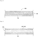
Fig. 3 is a cross-sectional view illustrating a circuit in a state where a resin laminate is formed. -
Fig. 4 is a cross-sectional view illustrating the circuit in a state where wiring is formed on the resin laminate. -
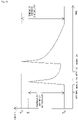
Fig. 5 is a graph illustrating a temperature change of an ultraviolet curable resin when a resin laminate is formed by a method in the conventional art. -
Fig. 6 is a graph illustrating a temperature change of the ultraviolet curable resin when the resin laminate is formed by the method in the conventional art. -
Fig. 7 is a graph illustrating a relationship between a difference in expansion coefficient and a temperature difference of the ultraviolet curable resin when irradiated with ultraviolet rays. -
Fig. 8 is a graph illustrating a temperature change of an ultraviolet curable resin when a resin laminate is formed by a method of the present invention. - Hereinafter, as exemplary embodiments of the present invention, an embodiment of the present invention is described in detail with reference to the drawings.
-
Fig. 1 illustratescircuit formation device 10.Circuit formation device 10 is provided withconveyance device 20,first shaping unit 22,second shaping unit 24, and control device 26 (refer toFig. 2 ).Conveyance device 20,first shaping unit 22, andsecond shaping unit 24 are disposed onbase 28 ofcircuit formation device 10.Base 28 has a substantially rectangular shape, and in the following description, the longitudinal direction ofbase 28 will be referred to as the X-axis direction, the shorter direction ofbase 28 will be referred to as the Y-axis direction, and the direction orthogonal to both the X-axis direction and the Y-axis direction will be referred to as the Z-axis direction. -
Conveyance device 20 is provided withX-axis slide mechanism 30 and Y-axis slide mechanism 32.X-axis slide mechanism 30 includesX-axis slide rail 34 andX-axis slider 36.X-axis slide rail 34 is disposed onbase 28 so as to extend in the X-axis direction.X-axis slider 36 is held byX-axis slide rail 34 so as to be slidable in the X-axis direction. Furthermore,X-axis slide mechanism 30 includes electromagnetic motor (refer toFig. 2 ) 38, and movesX-axis slider 36 to any position in the X-axis direction by drivingelectromagnetic motor 38. In addition, Y-axis slide mechanism 32 includes Y-axis slide rail 50 andstage 52. Y-axis slide rail 50 is disposed onbase 28 so as to extend in the Y-axis direction and is movable in the X-axis direction. One end portion of Y-axis slide rail 50 is coupled toX-axis slider 36.Stage 52 is held on Y-axis slide rail 50 to be slidable in the Y-axis direction. Furthermore, Y-axis slide mechanism 32 includes electromagnetic motor (refer toFig. 2 ) 56, andstage 52 moves to any position in the Y-axis direction by drivingelectromagnetic motor 56. As a result, by drivingX-axis slide mechanism 30 and Y-axis slide mechanism 32,stage 52 is moved to any position onbase 28 -
Stage 52 includesbase plate 60,holding device 62, lifting and lowering device (refer toFig. 2 ) 64, andcooling device 66.Base plate 60 is formed in a flat plate shape, and a board is placed on an upper surface ofbase plate 60.Holding devices 62 are provided on both side portions ofbase plate 60 in the X-axis direction. The board placed onbase plate 60 is fixedly held by interposing both edge portions of the board in the X-axis direction withholding devices 62. In addition, lifting and loweringdevice 64 is disposed belowbase plate 60, and lifts and lowersbase plate 60. Furthermore,cooling device 66 is disposed insidebase plate 60 tocool base plate 60 to a predetermined temperature. -
First shaping unit 22 is a unit for shaping wiring on board 70 (refer toFig. 3 ) placed onbase plate 60 ofstage 52, and includesfirst printing section 72 anddrying section 74.First printing section 72 includes ink jet head 76 (refer toFig. 2 ), and discharges metal ink linearly onboard 70 placed onbase plate 60. Metal ink is ink in which fine metal particles are dispersed in a solvent.Inkjet head 76 discharges a conductive material from multiple nozzles, for example, by a piezo method using a piezoelectric element. -
Drying section 74 includes ultraviolet irradiation device 78 (refer toFig. 2 ).Ultraviolet irradiation device 78 is a device for irradiating the metal ink discharged onboard 70 with ultraviolet rays, and the metal ink is dried by irradiating with ultraviolet rays. At this time, the solvent is vaporized by the drying of the metal ink, and the metal fine particles contact or aggregate with each other, and thus metal wiring is formed. - In addition,
second shaping unit 24 is a unit for shaping a resin layer onboard 70 placed onbase plate 60 ofstage 52, and includessecond printing section 84 andcuring section 86.Second printing section 84 includes ink jet head 88 (refer toFig. 2 ), and discharges the ultraviolet curable resin ontoboard 70 placed onbase plate 60.Ink jet head 88 may be, for example, a piezo method using a piezoelectric element, or may be a thermal method in which a resin is heated to generate air bubbles and discharged from a nozzle. -
Curing section 86 includes flattening device (refer toFig. 2 ) 90 and irradiation device (refer toFig. 2 ) 92.Flattening device 90 is a device for flattening an upper surface of the ultraviolet curable resin discharged onboard 70 byink jet head 88, and makes the thickness of the ultraviolet curable resin uniform, for example, by scraping off excess resin by a roller or a blade while leveling the surface of the ultraviolet curable resin. In addition,irradiation device 92 is provided with a mercury lamp or LED as a light source, and irradiates the ultraviolet curable resin discharged onboard 70 with ultraviolet rays. As a result, the ultraviolet curable resin discharged onboard 70 is cured, and a resin layer is shaped. - In addition, as illustrated in
Fig. 2 ,control device 26 is provided withcontroller 120 andmultiple drive circuits 122.Multiple drive circuits 122 are connected to aboveelectromagnetic motors holding device 62, lifting andlowering device 64,cooling device 66,ink jet head 76,ultraviolet irradiation device 78,ink jet head 88,flattening device 90, andirradiation device 92.Controller 120 is provided with CPU, ROM, RAM, and the like, and is mainly a computer, and is connected tomultiple drive circuits 122. As a result, the operations ofconveyance device 20,first shaping unit 22, andsecond shaping unit 24 are controlled bycontroller 120. - In
circuit formation device 10, a circuit pattern is formed onboard 70 by the above-described configuration. Specifically,board 70 is set onbase plate 60 ofstage 52, andstage 52 is moved below second shapingunit 24. Insecond shaping unit 24,resin laminate 130 is formed onboard 70 as illustrated inFig. 3 .Resin laminate 130 is formed by repeating discharge of the ultraviolet curable resin fromink jet head 88 and irradiation of the discharged ultraviolet curable resin with ultraviolet rays byirradiation device 92. - More specifically, in
second printing section 84 ofsecond shaping unit 24,ink jet head 88 discharges the ultraviolet curable resin in a thin film shape onto an upper surface ofboard 70. Subsequently, when the ultraviolet curable resin is discharged in a thin film shape, the ultraviolet curable resin is flattened by flatteningdevice 90 in curingsection 86, so that the ultraviolet curable resin has a uniform film thickness.Irradiation device 92 irradiates the thin film-shaped ultraviolet curable resin with ultraviolet rays. As a result, thin film-shapedresin layer 132 is formed onboard 70. - Subsequently,
ink jet head 88 discharges the ultraviolet curable resin in a thin film shape onto thin film-shapedresin layer 132. The thin film-shaped ultraviolet curable resin is flattened by flatteningdevice 90,irradiation device 92 irradiates the ultraviolet curable resin discharged in a thin film shape with ultraviolet rays, and thus thin film-shapedresin layer 132 is laminated on thin film-shapedresin layer 132. As described above, the discharge of the ultraviolet curable resin onto thin film-shapedresin layer 132 and the irradiation of ultraviolet rays are repeated, andmultiple resin layers 132 are laminated, and thusresin laminate 130 is formed. - When
resin laminate 130 is formed by the above-described procedure,stage 52 is moved below first shapingunit 22. Infirst printing section 72, as illustrated inFig. 4 ,ink jet head 76 linearly dischargesmetal ink 134 on the upper surface ofresin laminate 130 in accordance with the circuit pattern. Next, in dryingsection 74 offirst shaping unit 22,ultraviolet irradiation device 78 irradiatesmetal ink 134 with ultraviolet rays. As a result,metal ink 134 is dried, andwiring 136 is formed onresin laminate 130. - As described above, in
circuit formation device 10,resin laminate 130 is formed by curing the ultraviolet curable resin, andwiring 136 is formed by drying the metal ink, and thus the circuit pattern is formed onboard 70. Each ofmultiple resin layers 132 to be laminated when formingresin laminate 130 is formed by curing the thin film-shaped ultraviolet curable resin by irradiating the ultraviolet curable resin applied in a thin film shape with ultraviolet rays having a required integrated amount of light, which is the amount of light required to cure the ultraviolet curable resin. At this time, whenresin laminate 130 in the conventional art is formed,resin layer 132 is formed by irradiating the thin film-shaped ultraviolet curable resin with ultraviolet rays having a required integrated amount of light at once. That is, the thin film-shaped ultraviolet curable resin is cured by irradiating the thin film-shaped ultraviolet curable resin with ultraviolet rays once, and thusresin layer 132 is formed. - As described above, when the ultraviolet ray having the required integrated amount of light is irradiated to the ultraviolet curable resin at once, the curing reaction of the ultraviolet curable resin proceeds at once, and high reaction heat is generated. In addition, when the ultraviolet curable resin absorbs ultraviolet rays having a required integrated amount of light, high absorption heat is also generated. Therefore, the ultraviolet curable resin is heated to a high temperature, and
resin layer 132 having a high temperature is formed. In addition, as the temperature of the ultraviolet curable resin rises,board 70 to which the ultraviolet curable resin is applied also reaches a high temperature. Afterresin layer 132 is formed, in a process in which the temperature betweenresin layer 132 andboard 70 that are at a high temperature is reduced, there is a possibility thatresin layer 132 is warped due to the difference in shrinkage betweenresin layer 132 andboard 70. At this time, the difference in shrinkage betweenresin layer 132 andboard 70 is significantly affected by the difference in the expansion coefficient ofresin layer 132 and the expansion coefficient ofboard 70, and the temperature difference of the ultraviolet curable resin when irradiated with ultraviolet rays. - The expansion coefficient indicates the ratio per unit temperature at which the object expands as the temperature of the object increases, and is also referred to as a coefficient of thermal expansion. For example, the elongation rate of the length due to the expansion of the object per unit temperature is referred to as a linear coefficient of thermal expansion, and the increase rate of the volume due to the expansion of the object per unit temperature is referred to as a volume coefficient of thermal expansion. The larger the difference between the expansion coefficient of
resin layer 132 and the expansion coefficient ofboard 70, the larger the difference in shrinkage betweenresin layer 132 andboard 70 when the temperature is reduced betweenresin layer 132 andboard 70, and thus there is a possibility that a large warp may occur inresin layer 132. - In addition, the temperature difference between the ultraviolet curable resin when irradiated with ultraviolet rays (hereinafter, referred to as a "temperature difference when irradiated") is a difference between an ordinary temperature of the ultraviolet curable resin and the temperature of the ultraviolet curable resin when irradiated with ultraviolet rays. Specifically, the ordinary temperature of the ultraviolet curable resin is the temperature of the ultraviolet curable resin in a state of being not cooled or heated, and is substantially the same as the room temperature in an environment where
circuit formation device 10 is disposed, for example, in a room. As illustrated inFig. 5 , by irradiating the ultraviolet curable resin at ordinary temperature T0 with ultraviolet rays having a required integrated amount of light at once, the ultraviolet curable resin is cured to formresin layer 132. At this time, the temperature of the cured ultraviolet curable resin, that is,resin layer 132 rises to T1. Incidentally, temperature T1 of the cured ultraviolet curable resin, that is, temperature T1 of the ultraviolet curable resin when irradiated with ultraviolet rays having the required integrated amount of light is 100°C or higher. At this time, the temperature ofboard 70 is also 100°C or higher. The temperature betweenresin layer 132 andboard 70 increased to 100°C or higher is reduced to ordinary temperature T0 by heat dissipation. At this time, the larger the temperature difference between ordinary temperature T0 of the ultraviolet curable resin and temperature T1 of the ultraviolet curable resin when irradiated with ultraviolet rays, that is, the larger the temperature difference when irradiated, the larger the difference in shrinkage betweenresin layer 132 andboard 70, and there is a possibility that a large warp may occur inresin layer 132. InFig. 2 , the temperature change of the ultraviolet curable resin when tworesin layers 132 are formed is illustrated. That is, the temperature change of the ultraviolet curable resin when the formation ofresin layer 132 by the applying of the ultraviolet curable resin and the curing of the ultraviolet curable resin is performed twice is illustrated. - In addition, when
resin laminate 130 is formed, the ultraviolet curable resin is applied onresin layer 132 before temperature T1 of the ultraviolet curable resin when irradiated with ultraviolet rays is reduced to ordinary temperature To, and the ultraviolet curable resin may be irradiated with ultraviolet rays. In such a case, the temperature difference when irradiated for formingresin layer 132 increases, and there is a possibility that a further large warp may occur inresin layer 132. - That is, in
Fig. 5 , afterresin layer 132 on a first layer is formed, temperature T1 of the ultraviolet curable resin when irradiated with ultraviolet rays is reduced to ordinary temperature To, an ultraviolet curable resin on a second layer is applied onresin layer 132 on the first layer, and the ultraviolet curable resin on the second layer is irradiated with ultraviolet rays. At this time, the temperature difference when irradiated for formingresin layer 132 on the first layer is substantially the same as the temperature difference when irradiated for formingresin layer 132 on a second layer. - On the other hand, in
Fig. 3 , beforeresin layer 132 on the first layer is formed and temperature T1 of the ultraviolet curable resin when irradiated with ultraviolet rays is reduced to ordinary temperature To, the ultraviolet curable resin on the second layer is applied onresin layer 132 on the first layer, and the ultraviolet curable resin on the second layer is irradiated with ultraviolet rays. At this time, the temperature difference when irradiated for formingresin layer 132 on the second layer is larger than the temperature difference when irradiated for formingresin layer 132 on the first layer, and there is a possibility that a further large warp may occur inresin layer 132. Whenresin layer 132 is formed,resin layer 132 andboard 70 are separated from each other due to a large warp ofresin layer 132, and the shaping accuracy ofresin layer 132 is reduced. In addition, in a case whereresin layer 132 is aligned to a large extent, there is a possibility thatink jet head 88 or the like may come in contact with a portion ofresin layer 132 that warps upward whenresin layer 132 is formed. In addition, in order to suppress the separation ofresin layer 132 fromboard 70 due to the warpage, the adhesion ofresin layer 132 to board 70 is enhanced and the selection of the raw material of the ultraviolet curable resin is limited. At this time, whenresin layer 132 is separated in a state where the adhesion ofresin layer 132 to board 70 is high, the mechanical stress onboard 70 is significantly increased. In other words, the shaping accuracy ofresin laminate 130 during the formation ofresin layer 132 is also reduced. - In view of this fact, in
circuit formation device 10,cooling device 66 is disposed onbase plate 60, and the ultraviolet curable resin is irradiated with ultraviolet rays whilebase plate 60 is cooled by coolingdevice 66. At this time, coolingdevice 66 coolsbase plate 60 so that the temperature difference when irradiated is within a set temperature. The set temperature here is set based on the difference between the expansion coefficient ofresin layer 132 and the expansion coefficient ofboard 70. - Specifically, the amount of warpage of
resin laminate 130 when formingresin laminate 130 is indexed by the warpage radius of the portion where the warpage ofresin laminate 130 occurs. The warpage radius of the portion where the warpage ofresin laminate 130 occurs is the radius of the circular arc in a case where the portion where the warpage ofresin laminate 130 occurs is the circular arc, and is also referred to as a radius of curvature. Allowable value R is set for the amount of warpage ofresin laminate 130, and in a case where the thickness ofresin laminate 130 is L, the acceptance ofresin laminate 130 is determined according to the following equation.
- Y is a temperature difference between the ultraviolet curable resin when irradiated with ultraviolet rays, that is, a temperature difference when irradiated, and X is a difference between the expansion coefficient of
resin layer 132 and the expansion coefficient of board 70 (hereinafter, referred to as a "difference in expansion coefficient"). - Here, when the above equation is illustrated in a graph, a curve as illustrated in
Fig. 7 is obtained. A region below the curve is an acceptable region, and a region above the curve is a nonacceptable region. Therefore, for example, in a case where the difference in expansion coefficient is Xo, a set temperature difference is set so as to be smaller than Yo. That is, for example, in a case where Yo is 60°C, the set temperature difference is set to 50°C. In a case where the set temperature difference is set to 50°C,base plate 60 is cooled so that the temperature difference of the ultraviolet curable resin when irradiated with ultraviolet rays is within 50°C - Specifically, for example, in a case where the ordinary temperature of the ultraviolet curable resin is 25°C and the temperature of the ultraviolet curable resin when irradiated with ultraviolet rays in a state where
base plate 60 is not cooled is 125°C, the temperature of the ultraviolet curable resin is increased by 100°C by the irradiation of ultraviolet rays. That is, the elevated temperature of the ultraviolet curable resin by the irradiation of ultraviolet rays is 100°C. Therefore, whenbase plate 60 is cooled to minus 25°C, the ultraviolet curable resin applied to board 70 is also cooled viaboard 70, and thus the temperature of the ultraviolet curable resin when irradiated with ultraviolet rays is 75°C even when the elevated temperature of the ultraviolet curable resin is 100°C. At this time, the difference between the temperature of the ultraviolet curable resin (75°C) when irradiated with ultraviolet rays and the ordinary temperature of the ultraviolet curable resin (25°C), that is, the temperature difference when irradiated is 50°C, which is within the set temperature difference. As described above, by coolingbase plate 60 so that the temperature difference when irradiated is within the set temperature, the ultraviolet curable resin when irradiated with ultraviolet rays is also cooled, and the amount of warpage ofresin laminate 130 is within the range of allowable value R even in a case where warpage occurs inresin laminate 130. As a result, it is possible to suitably suppress the amount of warpage ofresin laminate 130 when irradiated with ultraviolet rays. - However, there is a case where
base plate 60 cannot be cooled to minus 25°C due to the performance of coolingdevice 66. In such a case, the ultraviolet curable resin is not irradiated with ultraviolet rays having the required integrated amount of light at once, the ultraviolet curable resin is separately irradiated with ultraviolet rays through multiple steps, and the integrated amount of light of ultraviolet rays by multiple steps is defined as the required integrated amount of light. - Specifically, the number of times of irradiating ultraviolet rays to be separately irradiated through multiple steps is determined based on the performance of cooling
device 66 and the set temperature difference. Here, the performance of coolingdevice 66 is a lower limit value of the cooling temperature ofbase plate 60 by coolingdevice 66, and coolingdevice 66 can coolbase plate 60 to 5°C. In addition, the set temperature difference is calculated based on the difference in expansion coefficient as described above. In the above description, the set temperature difference is set to 50°C, which is a temperature lower than Yo, based on the difference in expansion coefficient Xo, and in this description, the set temperature difference is set to 0°C, which is a temperature lower than Y1 (refer toFig. 7 ), based on the difference in expansion coefficient X1 (refer toFig. 7 ) having a significantly large value. Therefore, it is necessary to coolbase plate 60 so that the temperature of the ultraviolet curable resin when irradiated with ultraviolet rays is kept at an ordinary temperature (25°C) of the ultraviolet curable resin. - On the other hand, as described above, the lower limit value of the cooling temperature of
base plate 60 by coolingdevice 66 is 5°C, andbase plate 60 cannot be cooled to a temperature lower than 5°C. Therefore, inboard 70 placed onbase plate 60 cooled to 5°C, when the ultraviolet curable resin applied onboard 70 is irradiated with ultraviolet rays, in order to set the temperature of the ultraviolet curable resin to the ordinary temperature (25°C) of the ultraviolet curable resin, it is necessary to keep the elevated temperature of the ultraviolet curable resin when irradiated with ultraviolet rays at 20°C. However, as described above, the elevated temperature of the ultraviolet curable resin in a case where the ultraviolet curable resin is collectively irradiated with ultraviolet rays having the required integrated amount of light at once is 100°C. Therefore, it is necessary to separately irradiate the ultraviolet curable resin with ultraviolet rays through multiple steps so that the elevated temperature of the ultraviolet curable resin when irradiated with ultraviolet rays is 1/5 temperature (20°C) of the elevated temperature (100°C) of the ultraviolet curable resin when irradiated with ultraviolet rays having the required integrated amount of light. - Here, in order to simplify the description, for example, it is assumed that the elevated temperature of the ultraviolet curable resin in a case where the ultraviolet curable resin is irradiated with the ultraviolet ray having the amount of light of 1/2 of the required integrated amount of light is 1/2 of the elevated temperature (100°C) of the ultraviolet curable resin when irradiated with the ultraviolet ray having the required integrated amount of light. That is, it is assumed that the elevated temperature of the ultraviolet curable resin in a case where the ultraviolet curable resin is irradiated with ultraviolet rays having the amount of light of 1/X of the required integrated amount of light is 1/X of the elevated temperature (100°C) of the ultraviolet curable resin when irradiated with ultraviolet rays having a required integrated amount of light. Under such an assumption, in order to set the elevated temperature of the ultraviolet curable resin when irradiated with ultraviolet rays to 1/5 temperature (20°C) of the elevated temperature (100°C) of the ultraviolet curable resin when irradiated with ultraviolet rays having the required integrated amount of light, the amount of light when irradiated with ultraviolet rays may be set to 1/5 of the required integrated amount of light. In a case where the amount of light when irradiated with ultraviolet rays is set to be 1/5 of the required integrated amount of light, it is necessary to irradiate ultraviolet rays having the amount of light of 1/5 of the required integrated amount of light five times in order to cure the ultraviolet curable resin, that is, to irradiate the ultraviolet curable resin with ultraviolet rays having a required integrated amount of light. As a result, the number of times of irradiating ultraviolet rays to be separately irradiated through multiple steps is determined to be five times.
- As described above, when the number of times of irradiating with ultraviolet rays to be separately irradiated through multiple steps is determined,
base plate 60 is cooled to 5°C so that the difference between the temperature of the ultraviolet curable resin when irradiated with ultraviolet rays and the ordinary temperature (25°C) of the ultraviolet curable resin is within the set temperature difference (0°C). That is,base plate 60 is cooled to 5°C so that the temperature of the ultraviolet curable resin when irradiated with ultraviolet rays is the ordinary temperature (25°C) of the ultraviolet curable resin. Ultraviolet rays having the required integrated amount of light are separately irradiated five times. That is, the ultraviolet curable resin is irradiated with ultraviolet rays having the amount of light of 1/5 of the required integrated amount of light at once, and the irradiation of ultraviolet rays is repeated five times. As a result, as illustrated inFig. 8 , inbase plate 60 cooled to 5°C, the temperature of the ultraviolet curable resin rises by 20°C each time the ultraviolet curable resin applied to board 70 is irradiated with ultraviolet rays once. Therefore, the temperature of the ultraviolet curable resin when irradiated with ultraviolet rays is the ordinary temperature (25°C) of the ultraviolet curable resin, and the temperature difference between the ultraviolet curable resin when irradiated with ultraviolet rays is within the set temperature difference (0°C). As described above, even in a case where coolingdevice 66 can only coolbase plate 60 to 5°C, by separately irradiating the ultraviolet curable resin with ultraviolet rays through multiple steps, the temperature difference between the ultraviolet curable resin when irradiated with ultraviolet rays can be within the set temperature difference (0°C), and the amount of warpage of the resin laminate can be suitably suppressed. - Incidentally, in the above embodiment,
circuit formation device 10 is an example of the cured resin formation device.Board 70 is an example of a base.Inkjet head 88 is an example of an applying device.Irradiation device 92 is an example of an irradiation device. - The present invention is not limited to the embodiment described above, and can be implemented in various embodiments with various modifications and improvements based on the knowledge of those skilled in the art. For example, although the set temperature difference is set to 0°C in the above embodiment, any temperature can be set as long as the temperature is lower than Y1 (refer to
Fig. 7 ) corresponding to the difference in expansion coefficient X1 (refer toFig. 7 ). - In addition, in the above embodiment, although the ultraviolet curable resin is indirectly cooled by cooling
device 66, that is, throughbase plate 60 andboard 70, the ultraviolet curable resin may be directly cooled. For example, a blowing device may be disposed abovebase plate 60, and the ultraviolet curable resin may be directly cooled by blowing air by the blowing device toward the ultraviolet curable resin applied onboard 70. - In addition, in the above embodiment, wiring 136 formed on
resin laminate 130 is formed by dryingmetal ink 134 byultraviolet irradiation device 78, and may be formed by overheatingmetal ink 134 by a heating furnace or the like. In addition, wiring 136 may be formed by firingmetal ink 134 by a laser irradiation device. - In addition, although the present invention is applied to
circuit formation device 10 and the method of forming a circuit in the above embodiment, the present invention may be applied to a formation device and a method of forming a 3D shaped object such as a figure as long as the object is formed by curing an ultraviolet curable resin. - 10: circuit formation device (cured resin formation device), 70: board (base), 88: ink jet head (applying device), 92: irradiation device
Claims (5)
- A cured resin formation method comprising:an applying step of applying an ultraviolet curable resin on a base; anda curing step of curing the ultraviolet curable resin by irradiating the ultraviolet curable resin applied in the applying step with ultraviolet rays, whereinin the curing step, the ultraviolet curable resin is irradiated with ultraviolet rays while cooling the ultraviolet curable resin, so that a difference between an ordinary temperature of the ultraviolet curable resin and a temperature of the ultraviolet curable resin when irradiated with ultraviolet rays is within a set temperature difference set in advance.
- The cured resin formation method according to claim 1, wherein
the set temperature difference is set based on an expansion coefficient of the base and an expansion coefficient of the ultraviolet curable resin. - The cured resin formation method according to claim 1 or 2, wherein
in the curing step, the ultraviolet curable resin is cured by irradiating the ultraviolet curable resin applied in the applying step with ultraviolet rays through multiple steps so that an integrated amount of light of ultraviolet rays through multiple steps is a required integrated amount of light, which is an amount of light required to cure the ultraviolet curable resin. - The cured resin formation method according to claim 3, wherein
the number of times of irradiation with ultraviolet rays in the curing step is determined based on an expansion coefficient of the base, an expansion coefficient of the ultraviolet curable resin, and the set temperature difference. - A cured resin formation device comprising:an applying device configured to apply an ultraviolet curable resin on a base; andan irradiation device configured to cure the ultraviolet curable resin by irradiating the ultraviolet curable resin applied by the applying device with ultraviolet rays, whereinthe irradiation device irradiates the ultraviolet curable resin with ultraviolet rays while cooling the ultraviolet curable resin so that a difference between an ordinary temperature of the ultraviolet curable resin and a temperature of the ultraviolet curable resin when irradiated with ultraviolet rays is within a set temperature difference set in advance.
Applications Claiming Priority (1)
| Application Number | Priority Date | Filing Date | Title |
|---|---|---|---|
| PCT/JP2019/029992 WO2021019718A1 (en) | 2019-07-31 | 2019-07-31 | Cured resin formation method and cured resin formation device |
Publications (3)
| Publication Number | Publication Date |
|---|---|
| EP4005776A1 true EP4005776A1 (en) | 2022-06-01 |
| EP4005776A4 EP4005776A4 (en) | 2022-07-27 |
| EP4005776B1 EP4005776B1 (en) | 2025-09-10 |
Family
ID=74229477
Family Applications (1)
| Application Number | Title | Priority Date | Filing Date |
|---|---|---|---|
| EP19939655.7A Active EP4005776B1 (en) | 2019-07-31 | 2019-07-31 | Cured resin formation method |
Country Status (4)
| Country | Link |
|---|---|
| US (1) | US11945886B2 (en) |
| EP (1) | EP4005776B1 (en) |
| JP (1) | JP7158589B2 (en) |
| WO (1) | WO2021019718A1 (en) |
Family Cites Families (12)
| Publication number | Priority date | Publication date | Assignee | Title |
|---|---|---|---|---|
| JP4281930B2 (en) * | 1998-12-19 | 2009-06-17 | 共同印刷株式会社 | Manufacturing method of color filter |
| JP3229871B2 (en) * | 1999-07-13 | 2001-11-19 | 松下電器産業株式会社 | Method for transferring fine shape and method for manufacturing optical component |
| JP3934841B2 (en) * | 1999-12-27 | 2007-06-20 | 京セラ株式会社 | Multilayer board |
| JP4726162B2 (en) * | 2000-06-16 | 2011-07-20 | 共同印刷株式会社 | Thin film device manufacturing method |
| JP3837736B2 (en) * | 2001-07-02 | 2006-10-25 | ウシオ電機株式会社 | Work stage of resist curing equipment |
| AU2003286397A1 (en) | 2002-12-03 | 2004-06-23 | Objet Geometries Ltd. | Process of and apparatus for three-dimensional printing |
| JP2008106152A (en) * | 2006-10-25 | 2008-05-08 | Asahi Kasei Corp | Cellulose-containing resin composite |
| JP2013067016A (en) | 2011-09-20 | 2013-04-18 | Keyence Corp | Three-dimensional shaping apparatus |
| JP2014221538A (en) * | 2013-05-14 | 2014-11-27 | 富士機械製造株式会社 | Formation method and formation apparatus |
| US10462909B2 (en) * | 2014-11-14 | 2019-10-29 | Fuji Corporation | Wiring board manufacturing method and wiring board manufacturing device |
| WO2017221347A1 (en) | 2016-06-22 | 2017-12-28 | 富士機械製造株式会社 | Circuit formation method and circuit formation device |
| JP6724974B2 (en) * | 2018-12-21 | 2020-07-15 | セイコーエプソン株式会社 | Sinter modeling method, liquid binder, and sinter model |
-
2019
- 2019-07-31 US US17/630,850 patent/US11945886B2/en active Active
- 2019-07-31 WO PCT/JP2019/029992 patent/WO2021019718A1/en not_active Ceased
- 2019-07-31 JP JP2021536538A patent/JP7158589B2/en active Active
- 2019-07-31 EP EP19939655.7A patent/EP4005776B1/en active Active
Also Published As
| Publication number | Publication date |
|---|---|
| EP4005776B1 (en) | 2025-09-10 |
| WO2021019718A1 (en) | 2021-02-04 |
| US11945886B2 (en) | 2024-04-02 |
| JPWO2021019718A1 (en) | 2021-02-04 |
| US20220298267A1 (en) | 2022-09-22 |
| JP7158589B2 (en) | 2022-10-21 |
| EP4005776A4 (en) | 2022-07-27 |
Similar Documents
| Publication | Publication Date | Title |
|---|---|---|
| US11006529B2 (en) | Circuit forming method | |
| US11439025B2 (en) | Method for forming circuit | |
| JP2014221538A (en) | Formation method and formation apparatus | |
| JP6926078B2 (en) | Circuit formation method and circuit formation device | |
| EP4005776B1 (en) | Cured resin formation method | |
| JPWO2016189577A1 (en) | Wiring formation method | |
| JPWO2017009922A1 (en) | Wiring forming method and wiring forming apparatus | |
| WO2017006412A1 (en) | Shaping device and shaping method | |
| JP2020077661A (en) | Circuit formation method | |
| EP4007458B1 (en) | Method for manufacturing circuit wiring by three-dimensional additive manufacturing | |
| JP7325532B2 (en) | 3D object manufacturing method and 3D object manufacturing device by layered manufacturing method | |
| JP6818154B2 (en) | Wiring forming method and wiring forming device | |
| EP4306299A1 (en) | Determination device | |
| JP7250964B2 (en) | CIRCUIT-FORMING APPARATUS AND CIRCUIT-FORMING METHOD | |
| JP2023131281A (en) | Electric circuit formation method and control program | |
| WO2021166139A1 (en) | Circuit forming method | |
| JP2023166848A (en) | Electric circuit forming method and electric circuit forming device | |
| JP7554282B2 (en) | 3D object manufacturing equipment | |
| JP7516576B2 (en) | Three-dimensional modeling device and pallet transfer method | |
| WO2019016920A1 (en) | Wiring forming method and wiring forming device | |
| JP6866198B2 (en) | Circuit forming device | |
| JP6808050B2 (en) | Wiring forming method and wiring forming device | |
| JPWO2017017726A1 (en) | 3D object modeling equipment | |
| WO2021084692A1 (en) | Discharge device |
Legal Events
| Date | Code | Title | Description |
|---|---|---|---|
| STAA | Information on the status of an ep patent application or granted ep patent |
Free format text: STATUS: THE INTERNATIONAL PUBLICATION HAS BEEN MADE |
|
| PUAI | Public reference made under article 153(3) epc to a published international application that has entered the european phase |
Free format text: ORIGINAL CODE: 0009012 |
|
| STAA | Information on the status of an ep patent application or granted ep patent |
Free format text: STATUS: REQUEST FOR EXAMINATION WAS MADE |
|
| 17P | Request for examination filed |
Effective date: 20220107 |
|
| AK | Designated contracting states |
Kind code of ref document: A1 Designated state(s): AL AT BE BG CH CY CZ DE DK EE ES FI FR GB GR HR HU IE IS IT LI LT LU LV MC MK MT NL NO PL PT RO RS SE SI SK SM TR |
|
| A4 | Supplementary search report drawn up and despatched |
Effective date: 20220629 |
|
| RIC1 | Information provided on ipc code assigned before grant |
Ipc: H05K 3/12 20060101ALN20220623BHEP Ipc: H05K 3/46 20060101ALI20220623BHEP Ipc: B29C 35/16 20060101ALI20220623BHEP Ipc: B29C 35/08 20060101ALI20220623BHEP Ipc: B33Y 30/00 20150101ALI20220623BHEP Ipc: B33Y 10/00 20150101ALI20220623BHEP Ipc: B29C 64/30 20170101ALI20220623BHEP Ipc: B29C 64/124 20170101AFI20220623BHEP |
|
| DAV | Request for validation of the european patent (deleted) | ||
| DAX | Request for extension of the european patent (deleted) | ||
| STAA | Information on the status of an ep patent application or granted ep patent |
Free format text: STATUS: EXAMINATION IS IN PROGRESS |
|
| 17Q | First examination report despatched |
Effective date: 20230425 |
|
| P01 | Opt-out of the competence of the unified patent court (upc) registered |
Effective date: 20230328 |
|
| GRAP | Despatch of communication of intention to grant a patent |
Free format text: ORIGINAL CODE: EPIDOSNIGR1 |
|
| STAA | Information on the status of an ep patent application or granted ep patent |
Free format text: STATUS: GRANT OF PATENT IS INTENDED |
|
| RIC1 | Information provided on ipc code assigned before grant |
Ipc: H05K 3/12 20060101ALN20250501BHEP Ipc: H05K 3/46 20060101ALI20250501BHEP Ipc: B29C 35/16 20060101ALI20250501BHEP Ipc: B29C 35/08 20060101ALI20250501BHEP Ipc: B33Y 50/02 20150101ALI20250501BHEP Ipc: B33Y 30/00 20150101ALI20250501BHEP Ipc: B33Y 10/00 20150101ALI20250501BHEP Ipc: B29C 64/393 20170101ALI20250501BHEP Ipc: B29C 64/30 20170101ALI20250501BHEP Ipc: B29C 64/124 20170101AFI20250501BHEP |
|
| INTG | Intention to grant announced |
Effective date: 20250508 |
|
| GRAS | Grant fee paid |
Free format text: ORIGINAL CODE: EPIDOSNIGR3 |
|
| GRAA | (expected) grant |
Free format text: ORIGINAL CODE: 0009210 |
|
| STAA | Information on the status of an ep patent application or granted ep patent |
Free format text: STATUS: THE PATENT HAS BEEN GRANTED |
|
| AK | Designated contracting states |
Kind code of ref document: B1 Designated state(s): AL AT BE BG CH CY CZ DE DK EE ES FI FR GB GR HR HU IE IS IT LI LT LU LV MC MK MT NL NO PL PT RO RS SE SI SK SM TR |
|
| REG | Reference to a national code |
Ref country code: GB Ref legal event code: FG4D |
|
| REG | Reference to a national code |
Ref country code: CH Ref legal event code: EP |
|
| REG | Reference to a national code |
Ref country code: DE Ref legal event code: R096 Ref document number: 602019075701 Country of ref document: DE |
|
| REG | Reference to a national code |
Ref country code: IE Ref legal event code: FG4D |
|
| PG25 | Lapsed in a contracting state [announced via postgrant information from national office to epo] |
Ref country code: NO Free format text: LAPSE BECAUSE OF FAILURE TO SUBMIT A TRANSLATION OF THE DESCRIPTION OR TO PAY THE FEE WITHIN THE PRESCRIBED TIME-LIMIT Effective date: 20251210 |
|
| REG | Reference to a national code |
Ref country code: LT Ref legal event code: MG9D |
|
| PG25 | Lapsed in a contracting state [announced via postgrant information from national office to epo] |
Ref country code: FI Free format text: LAPSE BECAUSE OF FAILURE TO SUBMIT A TRANSLATION OF THE DESCRIPTION OR TO PAY THE FEE WITHIN THE PRESCRIBED TIME-LIMIT Effective date: 20250910 |
|
| REG | Reference to a national code |
Ref country code: NL Ref legal event code: MP Effective date: 20250910 |
|
| PG25 | Lapsed in a contracting state [announced via postgrant information from national office to epo] |
Ref country code: HR Free format text: LAPSE BECAUSE OF FAILURE TO SUBMIT A TRANSLATION OF THE DESCRIPTION OR TO PAY THE FEE WITHIN THE PRESCRIBED TIME-LIMIT Effective date: 20250910 |
|
| PG25 | Lapsed in a contracting state [announced via postgrant information from national office to epo] |
Ref country code: GR Free format text: LAPSE BECAUSE OF FAILURE TO SUBMIT A TRANSLATION OF THE DESCRIPTION OR TO PAY THE FEE WITHIN THE PRESCRIBED TIME-LIMIT Effective date: 20251211 |
|
| PG25 | Lapsed in a contracting state [announced via postgrant information from national office to epo] |
Ref country code: SE Free format text: LAPSE BECAUSE OF FAILURE TO SUBMIT A TRANSLATION OF THE DESCRIPTION OR TO PAY THE FEE WITHIN THE PRESCRIBED TIME-LIMIT Effective date: 20250910 |
|
| PG25 | Lapsed in a contracting state [announced via postgrant information from national office to epo] |
Ref country code: LV Free format text: LAPSE BECAUSE OF FAILURE TO SUBMIT A TRANSLATION OF THE DESCRIPTION OR TO PAY THE FEE WITHIN THE PRESCRIBED TIME-LIMIT Effective date: 20250910 |
|
| PG25 | Lapsed in a contracting state [announced via postgrant information from national office to epo] |
Ref country code: BG Free format text: LAPSE BECAUSE OF FAILURE TO SUBMIT A TRANSLATION OF THE DESCRIPTION OR TO PAY THE FEE WITHIN THE PRESCRIBED TIME-LIMIT Effective date: 20250910 Ref country code: PL Free format text: LAPSE BECAUSE OF FAILURE TO SUBMIT A TRANSLATION OF THE DESCRIPTION OR TO PAY THE FEE WITHIN THE PRESCRIBED TIME-LIMIT Effective date: 20250910 |
|
| PG25 | Lapsed in a contracting state [announced via postgrant information from national office to epo] |
Ref country code: RS Free format text: LAPSE BECAUSE OF FAILURE TO SUBMIT A TRANSLATION OF THE DESCRIPTION OR TO PAY THE FEE WITHIN THE PRESCRIBED TIME-LIMIT Effective date: 20251210 |
|
| PG25 | Lapsed in a contracting state [announced via postgrant information from national office to epo] |
Ref country code: ES Free format text: LAPSE BECAUSE OF FAILURE TO SUBMIT A TRANSLATION OF THE DESCRIPTION OR TO PAY THE FEE WITHIN THE PRESCRIBED TIME-LIMIT Effective date: 20250910 |
|
| REG | Reference to a national code |
Ref country code: AT Ref legal event code: MK05 Ref document number: 1835457 Country of ref document: AT Kind code of ref document: T Effective date: 20250910 |
|
| PG25 | Lapsed in a contracting state [announced via postgrant information from national office to epo] |
Ref country code: NL Free format text: LAPSE BECAUSE OF FAILURE TO SUBMIT A TRANSLATION OF THE DESCRIPTION OR TO PAY THE FEE WITHIN THE PRESCRIBED TIME-LIMIT Effective date: 20250910 |
|
| PG25 | Lapsed in a contracting state [announced via postgrant information from national office to epo] |
Ref country code: SM Free format text: LAPSE BECAUSE OF FAILURE TO SUBMIT A TRANSLATION OF THE DESCRIPTION OR TO PAY THE FEE WITHIN THE PRESCRIBED TIME-LIMIT Effective date: 20250910 |
|
| PG25 | Lapsed in a contracting state [announced via postgrant information from national office to epo] |
Ref country code: AT Free format text: LAPSE BECAUSE OF FAILURE TO SUBMIT A TRANSLATION OF THE DESCRIPTION OR TO PAY THE FEE WITHIN THE PRESCRIBED TIME-LIMIT Effective date: 20250910 |
|
| PG25 | Lapsed in a contracting state [announced via postgrant information from national office to epo] |
Ref country code: IT Free format text: LAPSE BECAUSE OF FAILURE TO SUBMIT A TRANSLATION OF THE DESCRIPTION OR TO PAY THE FEE WITHIN THE PRESCRIBED TIME-LIMIT Effective date: 20250910 |
|
| PG25 | Lapsed in a contracting state [announced via postgrant information from national office to epo] |
Ref country code: IS Free format text: LAPSE BECAUSE OF FAILURE TO SUBMIT A TRANSLATION OF THE DESCRIPTION OR TO PAY THE FEE WITHIN THE PRESCRIBED TIME-LIMIT Effective date: 20260110 |
|
| PG25 | Lapsed in a contracting state [announced via postgrant information from national office to epo] |
Ref country code: CZ Free format text: LAPSE BECAUSE OF FAILURE TO SUBMIT A TRANSLATION OF THE DESCRIPTION OR TO PAY THE FEE WITHIN THE PRESCRIBED TIME-LIMIT Effective date: 20250910 Ref country code: PT Free format text: LAPSE BECAUSE OF FAILURE TO SUBMIT A TRANSLATION OF THE DESCRIPTION OR TO PAY THE FEE WITHIN THE PRESCRIBED TIME-LIMIT Effective date: 20260112 |
|
| PG25 | Lapsed in a contracting state [announced via postgrant information from national office to epo] |
Ref country code: EE Free format text: LAPSE BECAUSE OF FAILURE TO SUBMIT A TRANSLATION OF THE DESCRIPTION OR TO PAY THE FEE WITHIN THE PRESCRIBED TIME-LIMIT Effective date: 20250910 Ref country code: SK Free format text: LAPSE BECAUSE OF FAILURE TO SUBMIT A TRANSLATION OF THE DESCRIPTION OR TO PAY THE FEE WITHIN THE PRESCRIBED TIME-LIMIT Effective date: 20250910 |