EP4001906A1 - Gasempfindliche vorrichtung - Google Patents
Gasempfindliche vorrichtung Download PDFInfo
- Publication number
- EP4001906A1 EP4001906A1 EP20208978.5A EP20208978A EP4001906A1 EP 4001906 A1 EP4001906 A1 EP 4001906A1 EP 20208978 A EP20208978 A EP 20208978A EP 4001906 A1 EP4001906 A1 EP 4001906A1
- Authority
- EP
- European Patent Office
- Prior art keywords
- capacitor electrode
- gas
- gas sensitive
- sensitive device
- layer
- Prior art date
- Legal status (The legal status is an assumption and is not a legal conclusion. Google has not performed a legal analysis and makes no representation as to the accuracy of the status listed.)
- Granted
Links
- 239000003990 capacitor Substances 0.000 claims abstract description 197
- 238000009413 insulation Methods 0.000 claims abstract description 55
- 239000000758 substrate Substances 0.000 claims abstract description 17
- 238000001179 sorption measurement Methods 0.000 claims abstract description 10
- 238000003795 desorption Methods 0.000 claims abstract description 7
- 230000004044 response Effects 0.000 claims abstract description 6
- 239000012212 insulator Substances 0.000 claims description 23
- 230000003993 interaction Effects 0.000 claims description 5
- 238000000034 method Methods 0.000 abstract description 46
- 239000007789 gas Substances 0.000 description 248
- 239000010410 layer Substances 0.000 description 149
- OKTJSMMVPCPJKN-UHFFFAOYSA-N Carbon Chemical compound [C] OKTJSMMVPCPJKN-UHFFFAOYSA-N 0.000 description 30
- 229910021389 graphene Inorganic materials 0.000 description 30
- 238000005259 measurement Methods 0.000 description 21
- 230000008859 change Effects 0.000 description 17
- 239000002105 nanoparticle Substances 0.000 description 13
- 150000003839 salts Chemical class 0.000 description 11
- 238000004590 computer program Methods 0.000 description 7
- 239000000463 material Substances 0.000 description 7
- 229910052751 metal Inorganic materials 0.000 description 7
- 239000002184 metal Substances 0.000 description 7
- JCXJVPUVTGWSNB-UHFFFAOYSA-N Nitrogen dioxide Chemical compound O=[N]=O JCXJVPUVTGWSNB-UHFFFAOYSA-N 0.000 description 6
- 230000001419 dependent effect Effects 0.000 description 6
- 230000000694 effects Effects 0.000 description 6
- 238000000691 measurement method Methods 0.000 description 6
- 230000035945 sensitivity Effects 0.000 description 6
- 238000013461 design Methods 0.000 description 5
- 238000001514 detection method Methods 0.000 description 5
- 238000002847 impedance measurement Methods 0.000 description 5
- 238000003860 storage Methods 0.000 description 4
- 239000003570 air Substances 0.000 description 3
- 238000013459 approach Methods 0.000 description 3
- 230000002596 correlated effect Effects 0.000 description 3
- 230000000875 corresponding effect Effects 0.000 description 3
- 239000003989 dielectric material Substances 0.000 description 3
- 230000008569 process Effects 0.000 description 3
- 238000012545 processing Methods 0.000 description 3
- 238000004088 simulation Methods 0.000 description 3
- MGWGWNFMUOTEHG-UHFFFAOYSA-N 4-(3,5-dimethylphenyl)-1,3-thiazol-2-amine Chemical compound CC1=CC(C)=CC(C=2N=C(N)SC=2)=C1 MGWGWNFMUOTEHG-UHFFFAOYSA-N 0.000 description 2
- UGFAIRIUMAVXCW-UHFFFAOYSA-N Carbon monoxide Chemical compound [O+]#[C-] UGFAIRIUMAVXCW-UHFFFAOYSA-N 0.000 description 2
- CBENFWSGALASAD-UHFFFAOYSA-N Ozone Chemical compound [O-][O+]=O CBENFWSGALASAD-UHFFFAOYSA-N 0.000 description 2
- 229910003481 amorphous carbon Inorganic materials 0.000 description 2
- 229910002091 carbon monoxide Inorganic materials 0.000 description 2
- 238000004140 cleaning Methods 0.000 description 2
- 230000008021 deposition Effects 0.000 description 2
- 238000007306 functionalization reaction Methods 0.000 description 2
- 230000003071 parasitic effect Effects 0.000 description 2
- 229910021420 polycrystalline silicon Inorganic materials 0.000 description 2
- 229920005591 polysilicon Polymers 0.000 description 2
- 230000009467 reduction Effects 0.000 description 2
- 238000012935 Averaging Methods 0.000 description 1
- 229910002089 NOx Inorganic materials 0.000 description 1
- VYPSYNLAJGMNEJ-UHFFFAOYSA-N Silicium dioxide Chemical compound O=[Si]=O VYPSYNLAJGMNEJ-UHFFFAOYSA-N 0.000 description 1
- 238000009825 accumulation Methods 0.000 description 1
- 230000006978 adaptation Effects 0.000 description 1
- 238000003915 air pollution Methods 0.000 description 1
- 239000012080 ambient air Substances 0.000 description 1
- 239000002800 charge carrier Substances 0.000 description 1
- 210000001520 comb Anatomy 0.000 description 1
- 239000004020 conductor Substances 0.000 description 1
- 238000010276 construction Methods 0.000 description 1
- 238000007796 conventional method Methods 0.000 description 1
- 238000010168 coupling process Methods 0.000 description 1
- 238000005859 coupling reaction Methods 0.000 description 1
- 239000002019 doping agent Substances 0.000 description 1
- 238000001035 drying Methods 0.000 description 1
- 239000007772 electrode material Substances 0.000 description 1
- 230000007613 environmental effect Effects 0.000 description 1
- 239000012530 fluid Substances 0.000 description 1
- 230000006870 function Effects 0.000 description 1
- 238000010438 heat treatment Methods 0.000 description 1
- 239000004615 ingredient Substances 0.000 description 1
- 230000010354 integration Effects 0.000 description 1
- 238000004519 manufacturing process Methods 0.000 description 1
- 238000012544 monitoring process Methods 0.000 description 1
- 239000002086 nanomaterial Substances 0.000 description 1
- 125000001997 phenyl group Chemical group [H]C1=C([H])C([H])=C(*)C([H])=C1[H] 0.000 description 1
- 230000000704 physical effect Effects 0.000 description 1
- 239000004065 semiconductor Substances 0.000 description 1
- 229910052814 silicon oxide Inorganic materials 0.000 description 1
- 239000002356 single layer Substances 0.000 description 1
- 239000002904 solvent Substances 0.000 description 1
- 238000012360 testing method Methods 0.000 description 1
- 231100000331 toxic Toxicity 0.000 description 1
- 230000002588 toxic effect Effects 0.000 description 1
Images


Classifications
-
- G—PHYSICS
- G01—MEASURING; TESTING
- G01N—INVESTIGATING OR ANALYSING MATERIALS BY DETERMINING THEIR CHEMICAL OR PHYSICAL PROPERTIES
- G01N27/00—Investigating or analysing materials by the use of electric, electrochemical, or magnetic means
- G01N27/02—Investigating or analysing materials by the use of electric, electrochemical, or magnetic means by investigating impedance
- G01N27/22—Investigating or analysing materials by the use of electric, electrochemical, or magnetic means by investigating impedance by investigating capacitance
- G01N27/221—Investigating or analysing materials by the use of electric, electrochemical, or magnetic means by investigating impedance by investigating capacitance by investigating the dielectric properties
-
- G—PHYSICS
- G01—MEASURING; TESTING
- G01N—INVESTIGATING OR ANALYSING MATERIALS BY DETERMINING THEIR CHEMICAL OR PHYSICAL PROPERTIES
- G01N27/00—Investigating or analysing materials by the use of electric, electrochemical, or magnetic means
- G01N27/02—Investigating or analysing materials by the use of electric, electrochemical, or magnetic means by investigating impedance
- G01N27/04—Investigating or analysing materials by the use of electric, electrochemical, or magnetic means by investigating impedance by investigating resistance
- G01N27/12—Investigating or analysing materials by the use of electric, electrochemical, or magnetic means by investigating impedance by investigating resistance of a solid body in dependence upon absorption of a fluid; of a solid body in dependence upon reaction with a fluid, for detecting components in the fluid
- G01N27/125—Composition of the body, e.g. the composition of its sensitive layer
-
- G—PHYSICS
- G01—MEASURING; TESTING
- G01N—INVESTIGATING OR ANALYSING MATERIALS BY DETERMINING THEIR CHEMICAL OR PHYSICAL PROPERTIES
- G01N27/00—Investigating or analysing materials by the use of electric, electrochemical, or magnetic means
- G01N27/02—Investigating or analysing materials by the use of electric, electrochemical, or magnetic means by investigating impedance
- G01N27/04—Investigating or analysing materials by the use of electric, electrochemical, or magnetic means by investigating impedance by investigating resistance
- G01N27/12—Investigating or analysing materials by the use of electric, electrochemical, or magnetic means by investigating impedance by investigating resistance of a solid body in dependence upon absorption of a fluid; of a solid body in dependence upon reaction with a fluid, for detecting components in the fluid
-
- G—PHYSICS
- G01—MEASURING; TESTING
- G01N—INVESTIGATING OR ANALYSING MATERIALS BY DETERMINING THEIR CHEMICAL OR PHYSICAL PROPERTIES
- G01N27/00—Investigating or analysing materials by the use of electric, electrochemical, or magnetic means
- G01N27/02—Investigating or analysing materials by the use of electric, electrochemical, or magnetic means by investigating impedance
- G01N27/04—Investigating or analysing materials by the use of electric, electrochemical, or magnetic means by investigating impedance by investigating resistance
- G01N27/12—Investigating or analysing materials by the use of electric, electrochemical, or magnetic means by investigating impedance by investigating resistance of a solid body in dependence upon absorption of a fluid; of a solid body in dependence upon reaction with a fluid, for detecting components in the fluid
- G01N27/125—Composition of the body, e.g. the composition of its sensitive layer
- G01N27/127—Composition of the body, e.g. the composition of its sensitive layer comprising nanoparticles
-
- G—PHYSICS
- G01—MEASURING; TESTING
- G01N—INVESTIGATING OR ANALYSING MATERIALS BY DETERMINING THEIR CHEMICAL OR PHYSICAL PROPERTIES
- G01N27/00—Investigating or analysing materials by the use of electric, electrochemical, or magnetic means
- G01N27/02—Investigating or analysing materials by the use of electric, electrochemical, or magnetic means by investigating impedance
- G01N27/04—Investigating or analysing materials by the use of electric, electrochemical, or magnetic means by investigating impedance by investigating resistance
- G01N27/12—Investigating or analysing materials by the use of electric, electrochemical, or magnetic means by investigating impedance by investigating resistance of a solid body in dependence upon absorption of a fluid; of a solid body in dependence upon reaction with a fluid, for detecting components in the fluid
- G01N27/129—Diode type sensors, e.g. gas sensitive Schottky diodes
-
- G—PHYSICS
- G01—MEASURING; TESTING
- G01N—INVESTIGATING OR ANALYSING MATERIALS BY DETERMINING THEIR CHEMICAL OR PHYSICAL PROPERTIES
- G01N27/00—Investigating or analysing materials by the use of electric, electrochemical, or magnetic means
- G01N27/02—Investigating or analysing materials by the use of electric, electrochemical, or magnetic means by investigating impedance
- G01N27/22—Investigating or analysing materials by the use of electric, electrochemical, or magnetic means by investigating impedance by investigating capacitance
- G01N27/226—Construction of measuring vessels; Electrodes therefor
-
- G—PHYSICS
- G01—MEASURING; TESTING
- G01N—INVESTIGATING OR ANALYSING MATERIALS BY DETERMINING THEIR CHEMICAL OR PHYSICAL PROPERTIES
- G01N33/00—Investigating or analysing materials by specific methods not covered by groups G01N1/00 - G01N31/00
- G01N33/0004—Gaseous mixtures, e.g. polluted air
- G01N33/0009—General constructional details of gas analysers, e.g. portable test equipment
-
- G—PHYSICS
- G01—MEASURING; TESTING
- G01N—INVESTIGATING OR ANALYSING MATERIALS BY DETERMINING THEIR CHEMICAL OR PHYSICAL PROPERTIES
- G01N27/00—Investigating or analysing materials by the use of electric, electrochemical, or magnetic means
- G01N27/02—Investigating or analysing materials by the use of electric, electrochemical, or magnetic means by investigating impedance
- G01N27/22—Investigating or analysing materials by the use of electric, electrochemical, or magnetic means by investigating impedance by investigating capacitance
- G01N27/221—Investigating or analysing materials by the use of electric, electrochemical, or magnetic means by investigating impedance by investigating capacitance by investigating the dielectric properties
- G01N2027/222—Investigating or analysing materials by the use of electric, electrochemical, or magnetic means by investigating impedance by investigating capacitance by investigating the dielectric properties for analysing gases
Definitions
- the disclosure relates in general to a gas sensitive device and a method for operating the gas sensitive device.
- the disclosure especially refers to a multi-gas sensor.
- the deposition of an active sensor layer is a printing process of a solvent consisting of ink, graphene flakes and e.g. nanoparticles for functionalization.
- a solvent consisting of ink, graphene flakes and e.g. nanoparticles for functionalization.
- the fluid ink droplets form a so-called coffee-ring at the edge of the sensor area.
- the result is a thicker sensor layer at the sensor edge.
- the current is located at the sensor edge and not homogeneously distributed over the whole sensor area. Thus, only the small current path of the "Coffee-Ring" is contributing to the sensitivity and not the whole sensor area.
- An established concept is a printed or dispensed active sensor-layer consisting of graphene flakes and functional nanoparticles on top of an interdigital structure (as shown in Fig. 9b ). The adsorption or desorption of gas molecules are reflected by the change of the electrical resistance of the device.
- the metal lines of the interdigital structure can cause accumulation and clumping of ink ingredients between two metal fingers. In this case, also only a small area is defining the sensitivity and not the whole sensor area.
- a gas sensitive device comprises a substrate structure, and a gas sensitive capacitor.
- the gas sensitive capacitor comprises a first capacitor electrode in form of a gas-sensitive layer on a first main surface region of an insulation layer, and a second capacitor electrode in form of a buried conductive region below the insulation layer.
- the insulation layer is arranged between the first and second capacitor electrode; wherein the gas-sensitive layer comprises a sheet impedance which changes in response to the adsorption or desorption of gas molecules.
- the first capacitor electrode is preferably provided on top of the gas sensitive device. Therefore, the first capacitor electrode may be called top electrode.
- the second capacitor electrode is preferably buried and is provided in the gas sensitive device, in particular above a substrate structure carrying the gas sensitive device. Therefore, the second capacitor electrode may be called buried electrode.
- a gas sensitive layer on top of a flat surface forms the first capacity electrode, i.e. the top electrode, of a gas sensitive capacitor.
- the second capacity electrode of the capacitor is a buried electrode under a, preferably thin, insulation layer.
- the top electrode is contacted at the edge. Therefore, the inner part of the top electrode is contacted via the rather high ohmic gas sensitive layer. If gas molecules are adsorbed at the surface by the top electrode, the sheet resistance or sheet impedance will change. This can be measured with the methods described below.
- a multi-gas sensor comprises one or more gas sensitive devices according to any of the gas sensitive devices disclosed herein.
- the disclosed multi-gas sensor it may be possible to distinguish two or more gases with a sensor response of one gas sensitive device as proposed herein.
- a method for operating the gas sensitive device according to any of the gas sensitive devices disclosed herein comprises applying an AC signal to the first capacitor electrode; reading out a signal between the first capacitor electrode and the second capacitor electrode, wherein the signal read out comprises an information on the sheet resistance or the sheet impedance of the gas-sensitive layer of the first capacitor electrode due to the adsorbed or desorbed gas molecules.
- the relation between the sheet resistance or the sheet impedance of the sensitive layer and the capacitive impedance causes a frequency dependency of capacity measurement. At low frequencies the capacitance of the whole area can be measured. At high frequencies only the capacitance of the sensor edge can be measured.
- the proposed gas sensing capacitor is an averaging device. This means local non-homogeneities of the sensing layer are negligible. Also, the coffee ring effect has no negative effect to the gas detection.
- the proposed multi-gas sensor and the disclosed method can be implemented with any of the proposed gas-sensitive device described within this application.
- Embodiments of the present methods for providing calibration for a gas sensor device and for calibrating/testing a gas sensor device and embodiments of the gas sensor arrangement for providing calibration data and/or for calibrating the gas sensor device are described herein making reference to the appended drawings and figures.
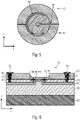
- Fig. 1 shows a schematic top view of a gas sensitive device 10 according to an embodiment
- Fig. 2 shows a schematic cross sectional view of the gas sensitive device 10 as shown in Fig. 1
- the gas sensitive device 10 comprises a substrate structure 20, and a gas sensitive capacitor.
- the gas sensitive capacitor comprises a first capacitor electrode 40 in form of a gas-sensitive layer 45 on a first main surface region of an insulation layer 30, and a second capacitor electrode 60 in form of a buried conductive region below the insulation layer 30.
- the insulation layer 30 is arranged between the first and second capacitor electrode 40, 60.
- the gas-sensitive layer 45 comprises a sheet resistance or a sheet impedance which changes in response to the adsorption or desorption of gas molecules.
- the first capacitor electrode 40 may for example be called a top electrode, because it is disposed on top of the gas sensitive device 10.
- the first capacitor electrode 40 is in contact with the ambient atmosphere allowing for adsorbing or desorbing gas molecules from the ambient atmosphere.
- the second capacitor electrode 60 is provided directly below the insulation layer 30 or directly below a stack of insulation layers 30 or between a stack of first insulation layers 30 and second insulation layers 35. It is possible that the insulation layer 30 and/or insulation layer 35 comprises a stack of different insulation layers 30, 35.
- the second capacitor electrode 60 may be disposed above the substrate structure 20, so that the second capacitor electrode 60 may be in contact on one side with the insulation layer 30 and on the opposite side may be in contact with the substrate structure 20.
- the first capacitor electrode 40 may be in contact on one side with the insulation layer 30, wherein the insulation layer 30 is a first insulation layer 30. On the opposite side the first capacitor electrode 40 may have an external surface region being in contact with the ambient atmosphere (see Fig. 2 ).
- the second capacitor electrode 60 may also be called the buried electrode.
- the gas sensitive layer 45 may have a thickness along the z-direction depending of the material, the thickness of the gas sensitive layer 45 can vary over a wide range. A preferred thickness would be in the range of a real two dimensional layer (e.g. a graphene monolayer) up to several nanometers, for example, about 40 nm.
- the first capacitor electrode 40 and second capacitor electrode 60 may be provided with contact regions 50, 70.
- the gas sensitive device 10 comprises a first contact region 50 for electrically contacting the first capacitor electrode 40, and a second contact region 70 for electrically contacting the second capacitor electrode 60.
- the gas sensitive device 10 may be provided with a contact hole 75 extending through the gas sensitive device 10 from the second contact region 70 to the second capacitor electrode 60.
- the insulation layer 30 between the first and second capacitor electrode 40, 60 may be a dielectric material, for example SiN.
- the core of the invention is an intelligent designed new capacitive gas sensitive device, with a new capacitive measurement method between a top and a buried electrode.
- the top electrode material is the gas sensitive layer 45 (e.g. graphene).
- the change of adsorbed gas molecules on the top electrode results in a change of the charge carrier density, which leads to a change of the AC impedance behavior.
- the proposed gas sensitive device 10 has an improved product performance expected due to the fact, that the gas detection with the new design will be no longer determined by lumps between the metal finger or the small coffee ring surrounding the sensor field, but by the much more bigger sensor area at the top of the gas sensitive device 10.
- Fig. 3 shows a schematic view of an equivalent circuit of the gas sensitive device 10 according to an embodiment.
- an equivalent circuit may be given by an RC-network.
- the first contact region 50 is ohmically coupled to the first capacitor electrode 40.
- Such a RC-network may have a frequency behavior depending in the adsorbed gas molecules. This means the sheet resistance or the sheet impedance of the top electrode or the first capacitor electrode 40 changes by the adsorption or desorption of gas molecules, for example of NO 2 (nitrogen dioxide), O 3 (ozone) or CO (carbon monoxide).
- Fig. 4 shows a schematic view of a graphene material, i.e. the two dimensional structure of the graphene doped with nanomaterials.
- Graphene is arranged in a two-dimensional honeycomb lattice, which may be doped with nanoparticles 42 or doped with salts. Depending on the chosen nanoparticles 42 or the salts, the graphene may become sensitive for the adsorption of specific gas molecules from the ambient atmosphere. By doping the graphene with nanoparticle and/or with salts the graphene becomes functionalized.
- the herein disclosed sensor principle also works with a not graphene based gas sensitive layer 45. Subject to the condition, that the used material is showing the described behavior.
- Examples of not graphene based layers 45 may be an amorphous Carbon, thin poly silicon, tantalnitride, titannitride, AIScN, or every material which forms a thin or two dimensional layer, which electrical conductivity can be influenced by the interaction with gas molecules.
- Fig. 9 shows a comparison between the proposed gas sensitive device (shown in Fig. 9a ) having an AC-coupled sensitive layer versus an established impedance measurement technique (shown in Fig. 9b ).
- an interdigital structure is necessary for performing the established AC-measurement technique. Then a lateral AC measurement can be performed in order to determine the real and the imaginary parts of the impedance Z.
- the established impedance measurement technique needs the interdigital structure in order to be per-formable.
- the proposed gas sensitive device 10 however, has a simple structure and allows also for measuring the impedance.
- Fig. 10 shows a schematic view of the gas sensitive device 10 coupled to an AC-measurement device and coupled to a DC voltage source.
- a sensitivity of the proposed gas sensitive device 10 can be adjusted by applying and adjusting a DC bias voltage V DC -bias. For doing so, the gas sensitive device 10 is connected with a DC voltage source 92 and with a AC measurement device 94 vie a bias T-component 96.
- Fig. 11 shows a theoretic explanation of the graphene band-structure.
- Fig. 11 also shows schematically the effect of adjusting the DC bias voltage until the so called "Dirac point" is reached.
- the graphene provides electron conduction or provides hole conduction. It was found that at the Dirac point the gas sensitive layer has its highest sensitivity for adsorbing gas molecules from the ambient atmosphere. It should be noted that the "Dirac point" is influenced by the functionalization of the gas sensitive layer 45, the (target) gas concentration and/or temperature.
- the regime at which the gas sensitive devices are sensitive or have a maximum sensitivity to ambient gases can be identified and, thus, can used for detecting gas molecules in the ambient atmosphere.
- the Dirac point of the gas sensitive device 10 can be determined from the local maximum of the DC-bias voltage V DC-Bias versus the resistance R.
- Fig. 12 and Fig. 13 show possible design variants for the gas sensitive area of the gas-sensitive device 10.
- a projection of the first capacitor electrode 40 vertically with respect to the first main surface region at least partially or completely overlaps with the second capacitor electrode 60.
- the Fig. 12 and the Fig. 13 show for example that different kinds of circle or parts of circles are possible to choose for the first and/or second capacitor electrodes 40, 60.
- the first and/or second capacitor electrodes 40, 60 may be formed, for example, as ellipses or parts of ellipses, polygons or part of polygons, meander or parts of meander, combs or parts of a comb. It is also possible to choose a combination of different geometries or a combination of different shapes. Also a free hand designed shape may be chosen (see Fig. 12 ). Also a different overlap sensing area to the underlying substrate structure 20 may be chosen (see Fig. 13 ).
- Fig. 13 also shows that a surrounding shape of the first electrode 40 may be different from a surrounding shape of the insulator layer 30 or wherein a surrounding shape of the first electrode 40 may be equal to a surrounding of the insulator layer 30. If different surrounding shapes of the insulator layer 30 and the first electrode 40 a partial overlap may result ( Fig. 13f ). Also a complete overlap may result according to the example shown in Fig. 13e , when different surrounding shapes of the insulator layer 30 and the first electrode 40 are used. Different configuration in which surrounding shape of the first electrode 40 may be equal to a surrounding of the insulator layer 30 are shown in Figs. 13a to 13d . As shown in Fig.
- the first electrode 40 completely or only partially overlaps the surface of the insulator layer 30.
- the insulator layer can be made of SiN and can have a thickness along the z-direction of about 150 nm to 200 nm.
- the insulator layer 30 can also be made of other dielectrics or can be made of a stack of different dielectrics, for example SiN/SiO/SiN or the like. The person skilled in the art is conscious about the correct molecule formula of SiO x and Si y N x , which are here abbreviated with SiO and SiN, respectively.
- the first contact region 50 at least partially or completely surrounds and electrically contacts the first capacitor electrode 40. Thereby, the first contact region 50 forms an area contact region or a point contact region with the first capacitor electrode 40.
- the second contact region 70 i.e. the second contact region 70 forms an area contact region or a point contact region with the second capacitor electrode 60 or with the second and a third capacitor electrode 60, 65.
- the first contact region 50 may be a full contact, surrounding fully or completely the gas sensitive layer 45. Also, the first contact region 50 may be a partial contact, only partially surrounding the gas sensitive layer 45 ( Fig. 14b ).
- the first contact region 50 may an area contact, having an area that is in contact with or next to the gas sensitive layer 45 ( Fig. 14c ). Furthermore, the first contact region 50 may be generated by a point contact, wherein only a point is in contact with the gas sensitive layer 45 ( Fig. 14d ). Furthermore, the first contact region 50 may be generated by any combination of the disclosed different kinds of contact ( Fig. 14e ). The disclosed example of the different contact regions, as shown on Fig. 14 may be used for the first capacitor electrode 40 and/or for the second capacitor electrode 60.
- the contact region 50 may be made of a metal or any other electrically conducting material.
- a cover layer 25 is disposed on top of the insulation layer 30 .
- the cover layer 25 has at least a common plane with the first contact region 50 and/ or with the first capacitor electrode 40, so that the cover layer 25 surrounds the first contact region 50 or the first contract region 50 and the first capacitor electrode 40 in the at least one common plane.
- Such embodiments are, for example shown in Figs. 2 , 6 , 16 , 17 and 18 .
- the cover layer 25 and at least the first contract region 50 and the first capacitor electrode 40 share a common plane, i.e. the cover layer 25 and at least the first contract region 50 and the first capacitor electrode 40 lie in the same common plane(s).
- the first contact region 50 extends from the first capacitor electrode 40 in the at least one common plane to a position above the cover layer 25 being in at least a plane parallel to the at least one common plane.
- the first contact region 50 contacts a first border region of the first capacitor electrode and extends along the -x direction (here the contact region extends on top of the insulation layer 30 in -x direction). Then first contact region 50 extends along the z direction and then along again the -x direction, i.e. the first contact region 50 extends on top or above the cover layer 25.
- the extension along the z direction corresponds to a thickness of the cover layer 25 along the z-direction.
- the Figs. Figs. 2 , 6 , 17, 17 and 18 for example show that the first border region of the first capacitor electrode 40 has a sloped curvature (i.e. is ramped) along x-z-direction.
- first contact regions 50 have in common that the first contact region 50 ohmically contacts a first border region of the first capacitor electrode 40, in particular the gas sensitive layer 45 of the top electrode. As shown in Fig. 14 , the first contact region 50 contacts the first border region of the first capacitor electrode 40 directly.
- the second buried capacitor electrode 60 may capacitively contact a center region of the first capacitor electrode 40.
- the buried third capacitor electrode 65 may capacitively contact a second border region of the first capacitor electrode 0.
- the second and third capacitor electrodes 60, 65 may be given by different kinds of partial contact, point contact or any combination of different contact form with the first capacitor electrode 40, i.e. the gas sensitive layer 45.
- the first capacitor electrode 40 may be given as a rectangle or square, as an ellipse or circle or any other geometry.
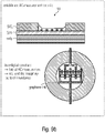
- Fig. 5 and Fig. 6 show a further embodiment.
- the capacitor electrode 40 is capacitively contacted by the second capacitor electrode 60 and the third capacitor electrode 65, i.e. by the two buried electrodes 60, 65.
- the buried second capacitor electrode 60 and the buried third capacitor electrode 65 are arranged in the same plane of the gas sensitive device 10.
- the second contact region 70 is coupled to the second capacitor electrode 60 or to the second and third capacitor electrodes 60, 65.
- the second contact region 70 and the second capacitor electrode 60 may be arranged in the same plane or in different planes of the gas sensitive device.
- the second contact region 70 and the second capacitor electrode 60 or the second and third capacitor electrodes 60, 65 are arranged in different planes of the gas sensitive device 10, these planes are parallel to each other. As shown in Fig. 6 the second and the third capacitor electrodes 60, 65 are separated along the x-y-directions by a second insulation layer 35 extending between the third capacitor electrode 65 and the second capacitor electrode 60.
- Fig. 15a to 15g show variations of the implementation of the gas sensitive device 10 as shown in Fig. 5 and Fig. 6 .
- the variations as shown in Fig. 15 show two buried electrodes 60, 65, i.e. the second capacitor electrode 60 and the third capacitor electrode 65, which may have the same or a different geometry to each other.
- Figs 15a, 15c, and Fig. 15e show implementations in which the second capacitor electrode 60 has a different geometry or shape from the third capacitor electrode.
- the two buried electrodes 60, 65 may have a line shape or a line shape combined with a point shape or any circle shape or any circle shape combined with a point shape, wherein the circle shape may comprise a full circle or any sub-circle shape.
- Fig. 7 shows a schematic view of a gas sensitive device 10 and of an equivalent circuit of an AC-coupled multi gas sensor 100 comprising four gas sensitive devices 10 according to an embodiment.
- the configuration of the gas sensitive device 10 is already described with reference to Figs. 1 and 2 .
- an equivalent circuit of the AC-coupled multi-gas sensor 100 is given by a RC-network.
- the sheet resistance is depending on the gas sensitive layer 45, in particular depending on the graphene layer.
- the resulting adsorption of gas molecules depends on the presence of the according gas molecules and the level of doping with nanoparticles or salts. Different chip layouts may be used for high frequency measurements or for low frequency measurements.
- each first capacity electrode 40 of each gas sensitive device 10 has one connection to an outer port 101, while each of the second capacity electrode 60 of the gas sensitive device 10 has a common single connection to an outer port.
- each of the first capacity electrodes 40 of each gas sensitive device 10 and each of the second capacity electrodes 40 of each gas sensitive device 10 has two connections to an outer port 101.
- each gas sensitive device 10 has four connections to outer ports, two gate-ports and two source ports.
- the four connections to outer ports enable a 2-Port NWA-measurement in "T-configuration", which neglects the impedances of the connection lines.
- the first capacity electrodes 40 are connected to the first port and the second capacity electrodes 60 are connected to the second port
- Z 11 U 1 I 1
- Z 21 U 2 I 1
- Z 22 U 2 I 2
- Z 12 U 1 I 2
- U is the voltage
- I the current
- Z the impedance according to the elements of the circuit shown in Fig. 7 .
- Z 3 is the impedance of the gas sensitive capacitor without any parasitics.
- Z 1 and Z 2 are the (parasitic) impedances of the connecting lines.
- the switching frequency is determined by the sheet resistance of the gas sensitive layer 45 and therefore by the adsorbed gas molecules. At low frequencies the sheet resistance of the sensitive layer is directly reflected in the real part of impedance.
- the gas sensitive capacitor enables different AC measurement capabilities (e.g. Lock-in technic, PPL, S-Parameter, as shown in Fig. 7 ).
- one of the advantages of AC-measurement methods is noise reduction.
- AC-measurement allows to distinguish between real and imagery impedance of the gas sensitive layer 45 and delivers therefore more information.
- the first main surface region of the insulation layer 30 having the gas-sensitive layer 45 is topology-free.
- the gas sensitive layer 45 is manufactured by dropping an ink drop onto the insulation layer 30. Because the gas-sensitive layer 45 according to the present disclosure has no topology, the influence of locally clustered graphene flakes and/or from coffee stain does not affect the gas-sensitive layer 45.
- the topology-freeness of the gas-sensitive layer 45 is shown throughout the Figures except Figs. in 4, 8, 11 and 20.
- the first capacitor electrode 40 and the second capacitor electrode 60 are arranged parallel to each other and vertical with respect to the first main surface region of the insulation layer 30.
- the first capacitor electrode 40 and the second capacitor electrode 60 are each arranged in parallel x-y planes, i.e. horizontal planes. Vertical means here along a z-direction.
- the insulation layer 30 between the first capacitor electrode 40 and the second capacitor electrode 60 is also called the first insulation layer 30.
- a third capacitor electrode 65 is disposed apart from the second capacitor electrode 60, wherein the third capacitor electrode 65 and the second capacitor electrode 60 are positioned so that both extend along in at least one common plane.
- Fig. 6 shows a gas sensitive device 10 having the second and the third capacitor electrodes 60, 65 lying on top of a second insulation layer 35.
- a contact region 70 for the second capacitor electrode 60 and a contact 70 for the third capacitor electrode 65 is disposed on top of the cover layer 25 .
- 65 contact holes 75 are provided for contacting the second and the third electrode 60.
- the contact holes 75 are, for example, etched.
- the contact holes 75 extend along the z-direction through the cover layer 25 and through the insulation layer 30.
- the third capacitor electrode 65 and the second capacitor electrode 60 are spaced apart from each other in the least one common plane by the second insulation layer 35 extending between third capacitor electrode 65 and the second capacitor electrode 60.
- the third capacitor electrode 65 and the second capacitor electrode 60 are spaced apart from each other by a part of the second insulation layer 35 extending between the third capacitor electrode 65 and the second capacitor electrode 60 along the z-direction.
- the second and the third capacitor electrodes 60, 65 are sandwiched between the first insulation layer 30 and the second insulation layer 35.
- the first capacitor electrode 40 being the gas sensitive layer 45 is a thin and/or two-dimensional layer 45, the electrical conductivity of which is influenceable by an interaction with gas molecules.
- the two-dimensional layer 45 may be a conductive graphene based layer.
- Graphene has a two-dimensional structure as shown in Fig. 4 .
- the two-dimensional structure comprises benzene rings, which may be doped with salts and/or nanoparticles 42.
- the first capacitor electrode 40 may also be a not graphene based gas sensitive layer 45. Subject to the condition, that the used material is showing the described behavior.
- Examples of not graphene based layers 45 may be an amorphous Carbon, thin poly silicon, tantalnitride, titannitride, AIScN, or every material which forms a thin or two dimensional layer, which electrical conductivity can be influenced by the interaction with gas molecules.
- the gas sensitive layer 45 or the thin and/or two-dimensional layer 45 is doped with nanoparticles and/or doped with salts for functionalizing the first electrode 40.
- a concentration of the doped nanoparticle or of the salts correlate to a concentration accuracy with which the adsorbed gas molecules can be measured.
- the nanoparticle and/or the salt used for doping determine which gas may be adsorbed. Stated differently, by changing the dopant another gas may be detectable.
- the gas sensitive device 10 comprises a heater 90 disposed or positioned in the gas sensitive device 10.
- the heater is used for bringing the gas-sensitive layer 45 to a desired temperature or temperature profile for sensing, or for resetting the gas-sensitive layer 45.
- the heater 90 and the second capacitor electrode 60 are separated from each other by the second insulation layer 35.
- the gas sensitive device 10 comprises a third contact region 80 for electrically contacting the heater 90, as for example shown in Figs. 16 , 17 or 18 .
- the heater 90 can be used for resetting or cleaning the gas sensitive layer 45. Cleaning or resetting means in this context to undo the adsorption of the gas molecules.
- the heater 90 comprises at least one side that at least partially forms with at least a side of the substrate layer 20 a cavity 100, as for example shown in Fig. 16 .
- the Figs. 17 and 18 show further examples of the cavity 100.
- the cavity 100 comprises at least one side of the substrate structure 20, at least one side of the heater 90 and at least one side of the second insulation layer 35.
- the cavity 100 comprises at least one side of the substrate structure 20, at least one side of the heater 90, at least one side of the second insulation layer 35 and at least one side of the second capacitor electrode 60.
- the cavity 100 is provided for thermal decoupling. In order to keep the necessary heating power small, to reach a target temperature.
- the cavity 100 is shown.
- Figs. 16 to 18 show different possible examples of where the heater 90 may be located in the gas sensitive device 10.
- a layout of the heater 90 can deviate from the examples as shown in the Figures, in particular the heater 90 may have different geometries.
- Figs. 16 and 17 show that the heater 90 is located below the second capacity electrode 60.
- the heater 90 extends in a x-y plane parallel to the second capacity electrode 60.
- the heater 90 is at least as long and as broad as the second capacity electrode 60.
- a diameter of the heater 90 in the x-y plane is either as large as or even larger than a diameter of the second capacity electrode 60.
- the heater 90 extends also in a x-y plane parallel to the second capacity electrode 60. However, the heater 90 forms a ring around the buried electrode. An inner perimeter of the heater ring is preferably lager than an outer perimeter of the buried electrode 60. Stated differently, the heater-ring 90 does not contact the buried electrode 60. In the cross section as shown in Fig. 17 the heater-ring seems like an interrupted heater structure.. In the cross sectional view of Fig. 17 , a length of the heater, in particular in the x-y plane, may be shorter than a length of the buried electrode. Furthermore, the heater 90 is not directly located beneath the second capacity electrode 60.
- the heater 90 and the second capacity electrode 60 build a kind of a chessboard pattern with the substrate structure 20.
- the heater 90 is again formed as a ring and surrounds the second capacity electrode 60, i.e. the heater 90 and the second capacity electrode 60 are disposed in the same plane.
- the heater 90 and the buried electrode 60 may be electrically separated by the insulator layer 30 or 35, for example by SiO or SiN.
- the gas sensitive device 10 may be provided with a plurality of first electrodes 40 on top of the insulator layer 30 and/or may be provided with a plurality of second electrodes 60 below the insulator layer 30.
- the gas sensitive device 10 may also be provided with both, a plurality of first and second contact regions 50, 70.
- the Figures except Figs. in 4, 8, 11 and 20 of the present application only show a single first contact region 50 and a single second contact region 70.
- a multi-gas sensor 100 is proposed.
- the multi-gas sensor comprises two or more gas sensitive devices 10 as disclosed herein.
- Fig. 19 shows an exemplary embodiment of a multi-gas sensor 100.
- the multi-gas sensor 100 shown in Fig. 19 for example is provided with four gas sensitive devices 10.
- Each of the gas sensitive devices 10 may be provided with a graphene layer or gas sensitive layer 45 that may be doped with different kinds of nanoparticles and/or salts.
- the multi-gas sensor 100 may become sensitive to the detection of different gas molecules and/or may become sensitive to different kinds of concentration levels of a particular gas molecule.
- a method for operating the gas sensitive device 10 is disclosed.
- Fig. 20 shows a flow chart of the principles of method for operating the gas sensitive device 10.
- the method 200 comprises applying an AC signal to the first capacitor electrode 40 according to a step 210 and reading out a signal between the first capacitor electrode 40 and the second capacitor electrode 60 according to step 220.
- the signal read out comprises an information on the sheet resistance of the gas-sensitive layer 45 of the first capacitor electrode 40 due to the adsorbed or desorbed gas molecules.
- Fig. 8 shows simulation results of different AC-measurement capabilities of the AC-coupled multi gas sensor when performing the proposed method 200. If measurements at low frequencies f are preformed, a change of the impedance Z will be detected.
- Figs. 8a and 8b show results for measurements or simulations at low frequencies f.
- the impedance Z is plotted against the applied frequency f of the AC-signal.
- the measured or simulated impedance Z is plotted against its corresponding sheet resistance R.
- the sheet resistance R is the real part of the sheet impedance Z that comprises an imaginary part and a real part. At low frequencies, i.e.
- the impedance change z and/or the resistance change R can be measured.
- the impedance change Z is correlated to the amount of adsorbed gas molecules.
- the impedance change Z may give a hint on the level of adsorbed gas molecules that are adsorbed by the gas sensitive layer 45.
- Fig. 8b shows the deviation of the sheet resistance in % (in percentage) form the normal value of the sheet resistance.
- the normal values of the sheet resistance of the gas sensitive layer 45 is given by the sheet resistance in atmosphere without pollution. Without pollution means without adsorbed molecules of the pollution, for example NO x , O 3 , CO 2 , CO or volantile organic components.
- the sheet resistance itself is always positive, however the deviation of the reference sheet resistance with the presence of adsorbed pollution molecules may be positive, zero or negative as can be seen in Fig. 8b .
- the sheet impedance at a low frequency f is correlated with the deviation of the sheet resistance R.
- the size of the value of the deviation of the sheet resistance may depend on the amount of adsorbed gas molecules.
- Figs. 8c and 8d show results for measurements or simulations at high frequencies f.
- High frequencies f are about 10 5 Hz.
- a detection of capacity changes will appear.
- the capacity change C is correlated with the change of the sheet resistance R.
- the capacity change C is measured to be the highest. Where no sheet resistance change R occurs, i.e. at a sheet resistance change of 0%, no capacity change occurs.
- the proposed method may further comprise applying an AC-signal to the gas sensitive capacitor; and measuring the capacitance / impedance of the whole area of the first electrode 40 at low frequencies, or measuring the capacitance at the edge of the first electrode 40 at high frequencies.
- the present proposed gas sensitive device which may be incorporated into a multi-gas sensor, provides an easy and cheap approach to determine the pollution of the ambient atmosphere with different kinds of gases, such a ozone O 3 , carbon monoxide CO, nitrogen dioxide NO 2 and many more different gases.
- the principle of the present disclosure is to provide the top electrode with a functionalized graphene layer, so that depending on the doped nanoparticles and/or doped salts different kinds of gas molecules can be detected.
- the top electrode thereby is provided by an ink drop with no specific topology.
- a gas sensitive device is provided that is independent from locally clustered graphene flakes and/or from coffee stain. Therewith, an approach to implement an improved gas sensitive device is disclosed.
- embodiments of the processing device can be implemented in hardware or in software or at least partially in hardware or at least partially in software.
- the implementation can be performed using a digital storage medium, for example a floppy disk, a DVD, a Blu-Ray, a CD, a ROM, a PROM, an EPROM, an EEPROM or a FLASH memory, having electronically readable control signals stored thereon, which cooperate (or are capable of cooperating) with a programmable computer system such that the respective method is performed. Therefore, the digital storage medium may be computer readable.
- Some embodiments comprise a data carrier having electronically readable control signals, which are capable of cooperating with a programmable computer system, such that one of the methods described herein is performed.
- embodiments of the processing device can be implemented as a computer program product with a program code, the program code being operative for performing one of the methods when the computer program product runs on a computer.
- the program code may for example be stored on a machine readable carrier.
- Other embodiments comprise the computer program for performing one of the methods described herein, stored on a machine readable carrier.
- an embodiment of the method is, therefore, a computer program having a program code for performing one of the methods described herein, when the computer program runs on a computer.
- a further embodiment of the methods is, therefore, a data carrier (or a digital storage medium, or a computer-readable medium) comprising, recorded thereon, the computer program for performing one of the methods described herein.
- the data carrier, the digital storage medium or the recorded medium are typically tangible and/or non-transitory.
- a further embodiment comprises a processing means, for example a computer, or a programmable logic device, configured to or adapted to perform one of the methods described herein.
- a further embodiment comprises a computer having installed thereon the computer program for performing one of the methods described herein.
- a programmable logic device for example a field programmable gate array
- a field programmable gate array may cooperate with a microprocessor in order to perform one of the methods described herein.
- the methods are preferably performed by any hardware apparatus.
- the apparatus described herein may be implemented using a hardware apparatus, or using a computer, or using a combination of a hardware apparatus and a computer.
- the methods described herein may be performed using a hardware apparatus, or using a computer, or using a combination of a hardware apparatus and a computer.
Landscapes
- Chemical & Material Sciences (AREA)
- Health & Medical Sciences (AREA)
- Life Sciences & Earth Sciences (AREA)
- Immunology (AREA)
- Physics & Mathematics (AREA)
- Analytical Chemistry (AREA)
- Biochemistry (AREA)
- General Health & Medical Sciences (AREA)
- General Physics & Mathematics (AREA)
- Pathology (AREA)
- Electrochemistry (AREA)
- Chemical Kinetics & Catalysis (AREA)
- Engineering & Computer Science (AREA)
- Combustion & Propulsion (AREA)
- Food Science & Technology (AREA)
- Medicinal Chemistry (AREA)
- Microelectronics & Electronic Packaging (AREA)
- Power Engineering (AREA)
- Nanotechnology (AREA)
- Investigating Or Analyzing Materials By The Use Of Electric Means (AREA)
- Investigating Or Analyzing Materials By The Use Of Fluid Adsorption Or Reactions (AREA)
Priority Applications (4)
| Application Number | Priority Date | Filing Date | Title |
|---|---|---|---|
| EP20208978.5A EP4001906B1 (de) | 2020-11-20 | 2020-11-20 | Gasempfindliche vorrichtung |
| US17/453,410 US11921074B2 (en) | 2020-11-20 | 2021-11-03 | Gas-sensitive device |
| KR1020210158586A KR20220069837A (ko) | 2020-11-20 | 2021-11-17 | 가스 감지 디바이스 |
| CN202111376473.8A CN114518388A (zh) | 2020-11-20 | 2021-11-19 | 气敏器件 |
Applications Claiming Priority (1)
| Application Number | Priority Date | Filing Date | Title |
|---|---|---|---|
| EP20208978.5A EP4001906B1 (de) | 2020-11-20 | 2020-11-20 | Gasempfindliche vorrichtung |
Publications (2)
| Publication Number | Publication Date |
|---|---|
| EP4001906A1 true EP4001906A1 (de) | 2022-05-25 |
| EP4001906B1 EP4001906B1 (de) | 2024-10-02 |
Family
ID=73543156
Family Applications (1)
| Application Number | Title | Priority Date | Filing Date |
|---|---|---|---|
| EP20208978.5A Active EP4001906B1 (de) | 2020-11-20 | 2020-11-20 | Gasempfindliche vorrichtung |
Country Status (4)
| Country | Link |
|---|---|
| US (1) | US11921074B2 (de) |
| EP (1) | EP4001906B1 (de) |
| KR (1) | KR20220069837A (de) |
| CN (1) | CN114518388A (de) |
Citations (4)
| Publication number | Priority date | Publication date | Assignee | Title |
|---|---|---|---|---|
| DE102011002854A1 (de) * | 2010-08-10 | 2012-02-16 | Robert Bosch Gmbh | Feldeffekt-Gassensor, Verfahren zur Herstellung eines Feldeffekt-Gassensors und Verfahren zur Detektion von Gas |
| US20150153297A1 (en) * | 2012-06-04 | 2015-06-04 | Commissariat A L'energie Atomique Et Aux Ene Alt | Capacitive humidity sensor with graphene electrode |
| US20190293596A1 (en) * | 2018-03-22 | 2019-09-26 | Kabushiki Kaisha Toshiba | Gas sensing method, gas sensor, and gas sensing system |
| EP3598118A1 (de) * | 2018-07-20 | 2020-01-22 | MEAS France | Kapazitative gassensoren und herstellungsverfahren dafür |
Family Cites Families (5)
| Publication number | Priority date | Publication date | Assignee | Title |
|---|---|---|---|---|
| US4953387A (en) * | 1989-07-31 | 1990-09-04 | The Regents Of The University Of Michigan | Ultrathin-film gas detector |
| AU2008307295B2 (en) * | 2007-10-05 | 2011-09-01 | 3M Innovative Properties Company | Organic chemical sensor comprising microporous polymer, and method of use |
| FR2934051B1 (fr) * | 2008-07-16 | 2011-12-09 | Commissariat Energie Atomique | Detecteur d'humidite capacitif a dielectrique hydrophile nanoporeux |
| EP2693207A1 (de) * | 2012-07-30 | 2014-02-05 | Nxp B.V. | Integrierte Schaltung mit kapazitativem Gassensor |
| US20140260545A1 (en) * | 2013-03-15 | 2014-09-18 | Infineon Technologies Ag | Sensor and sensing method |
-
2020
- 2020-11-20 EP EP20208978.5A patent/EP4001906B1/de active Active
-
2021
- 2021-11-03 US US17/453,410 patent/US11921074B2/en active Active
- 2021-11-17 KR KR1020210158586A patent/KR20220069837A/ko unknown
- 2021-11-19 CN CN202111376473.8A patent/CN114518388A/zh active Pending
Patent Citations (4)
| Publication number | Priority date | Publication date | Assignee | Title |
|---|---|---|---|---|
| DE102011002854A1 (de) * | 2010-08-10 | 2012-02-16 | Robert Bosch Gmbh | Feldeffekt-Gassensor, Verfahren zur Herstellung eines Feldeffekt-Gassensors und Verfahren zur Detektion von Gas |
| US20150153297A1 (en) * | 2012-06-04 | 2015-06-04 | Commissariat A L'energie Atomique Et Aux Ene Alt | Capacitive humidity sensor with graphene electrode |
| US20190293596A1 (en) * | 2018-03-22 | 2019-09-26 | Kabushiki Kaisha Toshiba | Gas sensing method, gas sensor, and gas sensing system |
| EP3598118A1 (de) * | 2018-07-20 | 2020-01-22 | MEAS France | Kapazitative gassensoren und herstellungsverfahren dafür |
Also Published As
| Publication number | Publication date |
|---|---|
| EP4001906B1 (de) | 2024-10-02 |
| US11921074B2 (en) | 2024-03-05 |
| US20220163475A1 (en) | 2022-05-26 |
| CN114518388A (zh) | 2022-05-20 |
| KR20220069837A (ko) | 2022-05-27 |
Similar Documents
| Publication | Publication Date | Title |
|---|---|---|
| JP5424794B2 (ja) | 薄膜型センシング部材を利用した化学センサ | |
| JP6533465B2 (ja) | ナノワイヤプラットフォームに基づく広いダイナミックレンジを持つ流体センサ | |
| TWI485604B (zh) | 觸摸檢測元件、觸控裝置及可攜式電子設備 | |
| CN105699463B (zh) | 一种化学场效应晶体管气敏传感器及其制造方法 | |
| JP5128581B2 (ja) | 磁性粒子測定デバイスおよび方法 | |
| US8395901B2 (en) | Vertically-stacked electronic devices having conductive carbon films | |
| EP2233920A1 (de) | Sensorvorrichtung und Verfahren zu seiner Herstellung | |
| KR100856577B1 (ko) | 탄소나노튜브 센서 및 그 제조방법 | |
| CN102369430A (zh) | 传感器装置及其制造方法 | |
| US11486848B2 (en) | Moisture sensor | |
| EP3208610B1 (de) | Sensoranordnung und verfahren zur erzeugung von messsignalen | |
| CN104849317B (zh) | 半导体感测装置及制作方法 | |
| Rivadeneyra et al. | Asymmetric enhanced surface interdigitated electrode capacitor with two out-of-plane electrodes | |
| EP4001906A1 (de) | Gasempfindliche vorrichtung | |
| Kato et al. | Influence of cell configuration on measuring interfacial impedances between a solid electrolyte and an electrode | |
| CN104793153A (zh) | 磁传感装置的制备方法 | |
| CN108693220B (zh) | 流体传感器、提供流体传感器的方法和确定流体组分的方法 | |
| CN103026169B (zh) | 测量多个器件中的层的厚度的方法及生产的器件 | |
| KR20110010929A (ko) | 나노와이어 트랜지스터 센서, 제조방법 및 이를 이용한 생체분자 검출장치 | |
| CN105486728A (zh) | 电容式湿度传感器及其制造方法 | |
| CN110364447B (zh) | 半导体工艺的关键尺寸的监测结构及监测方法 | |
| Ye et al. | Direct observation of surface charge redistribution in active nanoscale conducting channels by Kelvin Probe Force Microscopy | |
| CN108279266B (zh) | 电化学检测器 | |
| CN114646419B (zh) | 一种气体压强传感器及其制备方法和气体压强检测方法 | |
| EP3845895A1 (de) | Kapazitive sensoren mit unterschiedlichen messbereichen |
Legal Events
| Date | Code | Title | Description |
|---|---|---|---|
| PUAI | Public reference made under article 153(3) epc to a published international application that has entered the european phase |
Free format text: ORIGINAL CODE: 0009012 |
|
| STAA | Information on the status of an ep patent application or granted ep patent |
Free format text: STATUS: THE APPLICATION HAS BEEN PUBLISHED |
|
| AK | Designated contracting states |
Kind code of ref document: A1 Designated state(s): AL AT BE BG CH CY CZ DE DK EE ES FI FR GB GR HR HU IE IS IT LI LT LU LV MC MK MT NL NO PL PT RO RS SE SI SK SM TR |
|
| STAA | Information on the status of an ep patent application or granted ep patent |
Free format text: STATUS: REQUEST FOR EXAMINATION WAS MADE |
|
| 17P | Request for examination filed |
Effective date: 20220715 |
|
| RBV | Designated contracting states (corrected) |
Designated state(s): AL AT BE BG CH CY CZ DE DK EE ES FI FR GB GR HR HU IE IS IT LI LT LU LV MC MK MT NL NO PL PT RO RS SE SI SK SM TR |
|
| GRAP | Despatch of communication of intention to grant a patent |
Free format text: ORIGINAL CODE: EPIDOSNIGR1 |
|
| STAA | Information on the status of an ep patent application or granted ep patent |
Free format text: STATUS: GRANT OF PATENT IS INTENDED |
|
| INTG | Intention to grant announced |
Effective date: 20240314 |
|
| P01 | Opt-out of the competence of the unified patent court (upc) registered |
Effective date: 20240425 |
|
| GRAJ | Information related to disapproval of communication of intention to grant by the applicant or resumption of examination proceedings by the epo deleted |
Free format text: ORIGINAL CODE: EPIDOSDIGR1 |
|
| STAA | Information on the status of an ep patent application or granted ep patent |
Free format text: STATUS: REQUEST FOR EXAMINATION WAS MADE |
|
| GRAP | Despatch of communication of intention to grant a patent |
Free format text: ORIGINAL CODE: EPIDOSNIGR1 |
|
| STAA | Information on the status of an ep patent application or granted ep patent |
Free format text: STATUS: GRANT OF PATENT IS INTENDED |
|
| GRAS | Grant fee paid |
Free format text: ORIGINAL CODE: EPIDOSNIGR3 |
|
| INTC | Intention to grant announced (deleted) | ||
| GRAA | (expected) grant |
Free format text: ORIGINAL CODE: 0009210 |
|
| STAA | Information on the status of an ep patent application or granted ep patent |
Free format text: STATUS: THE PATENT HAS BEEN GRANTED |
|
| INTG | Intention to grant announced |
Effective date: 20240801 |
|
| AK | Designated contracting states |
Kind code of ref document: B1 Designated state(s): AL AT BE BG CH CY CZ DE DK EE ES FI FR GB GR HR HU IE IS IT LI LT LU LV MC MK MT NL NO PL PT RO RS SE SI SK SM TR |
|
| REG | Reference to a national code |
Ref country code: GB Ref legal event code: FG4D |