EP3989683B1 - Module substrate and semiconductor module including the same - Google Patents
Module substrate and semiconductor module including the same Download PDFInfo
- Publication number
- EP3989683B1 EP3989683B1 EP21187443.3A EP21187443A EP3989683B1 EP 3989683 B1 EP3989683 B1 EP 3989683B1 EP 21187443 A EP21187443 A EP 21187443A EP 3989683 B1 EP3989683 B1 EP 3989683B1
- Authority
- EP
- European Patent Office
- Prior art keywords
- groove
- module
- substrate
- wiring substrate
- contact pads
- Prior art date
- Legal status (The legal status is an assumption and is not a legal conclusion. Google has not performed a legal analysis and makes no representation as to the accuracy of the status listed.)
- Active
Links
Images




Classifications
-
- H—ELECTRICITY
- H10—SEMICONDUCTOR DEVICES; ELECTRIC SOLID-STATE DEVICES NOT OTHERWISE PROVIDED FOR
- H10W—GENERIC PACKAGES, INTERCONNECTIONS, CONNECTORS OR OTHER CONSTRUCTIONAL DETAILS OF DEVICES COVERED BY CLASS H10
- H10W70/00—Package substrates; Interposers; Redistribution layers [RDL]
- H10W70/60—Insulating or insulated package substrates; Interposers; Redistribution layers
- H10W70/67—Insulating or insulated package substrates; Interposers; Redistribution layers characterised by their insulating layers or insulating parts
- H10W70/68—Shapes or dispositions thereof
-
- H—ELECTRICITY
- H05—ELECTRIC TECHNIQUES NOT OTHERWISE PROVIDED FOR
- H05K—PRINTED CIRCUITS; CASINGS OR CONSTRUCTIONAL DETAILS OF ELECTRIC APPARATUS; MANUFACTURE OF ASSEMBLAGES OF ELECTRICAL COMPONENTS
- H05K3/00—Apparatus or processes for manufacturing printed circuits
- H05K3/40—Forming printed elements for providing electric connections to or between printed circuits
- H05K3/403—Edge contacts; Windows or holes in the substrate having plural connections on the walls thereof
-
- H—ELECTRICITY
- H05—ELECTRIC TECHNIQUES NOT OTHERWISE PROVIDED FOR
- H05K—PRINTED CIRCUITS; CASINGS OR CONSTRUCTIONAL DETAILS OF ELECTRIC APPARATUS; MANUFACTURE OF ASSEMBLAGES OF ELECTRICAL COMPONENTS
- H05K1/00—Printed circuits
- H05K1/02—Details
- H05K1/0266—Marks, test patterns or identification means
- H05K1/0268—Marks, test patterns or identification means for electrical inspection or testing
-
- H—ELECTRICITY
- H05—ELECTRIC TECHNIQUES NOT OTHERWISE PROVIDED FOR
- H05K—PRINTED CIRCUITS; CASINGS OR CONSTRUCTIONAL DETAILS OF ELECTRIC APPARATUS; MANUFACTURE OF ASSEMBLAGES OF ELECTRICAL COMPONENTS
- H05K1/00—Printed circuits
- H05K1/02—Details
- H05K1/0213—Electrical arrangements not otherwise provided for
-
- H—ELECTRICITY
- H05—ELECTRIC TECHNIQUES NOT OTHERWISE PROVIDED FOR
- H05K—PRINTED CIRCUITS; CASINGS OR CONSTRUCTIONAL DETAILS OF ELECTRIC APPARATUS; MANUFACTURE OF ASSEMBLAGES OF ELECTRICAL COMPONENTS
- H05K1/00—Printed circuits
- H05K1/02—Details
- H05K1/0296—Conductive pattern lay-out details not covered by sub groups H05K1/02 - H05K1/0295
- H05K1/0298—Multilayer circuits
-
- H—ELECTRICITY
- H05—ELECTRIC TECHNIQUES NOT OTHERWISE PROVIDED FOR
- H05K—PRINTED CIRCUITS; CASINGS OR CONSTRUCTIONAL DETAILS OF ELECTRIC APPARATUS; MANUFACTURE OF ASSEMBLAGES OF ELECTRICAL COMPONENTS
- H05K1/00—Printed circuits
- H05K1/02—Details
- H05K1/11—Printed elements for providing electric connections to or between printed circuits
- H05K1/111—Pads for surface mounting, e.g. lay-out
- H05K1/112—Pads for surface mounting, e.g. lay-out directly combined with via connections
-
- H—ELECTRICITY
- H05—ELECTRIC TECHNIQUES NOT OTHERWISE PROVIDED FOR
- H05K—PRINTED CIRCUITS; CASINGS OR CONSTRUCTIONAL DETAILS OF ELECTRIC APPARATUS; MANUFACTURE OF ASSEMBLAGES OF ELECTRICAL COMPONENTS
- H05K1/00—Printed circuits
- H05K1/02—Details
- H05K1/11—Printed elements for providing electric connections to or between printed circuits
- H05K1/115—Via connections; Lands around holes or via connections
- H05K1/116—Lands, clearance holes or other lay-out details concerning the surrounding of a via
-
- H—ELECTRICITY
- H05—ELECTRIC TECHNIQUES NOT OTHERWISE PROVIDED FOR
- H05K—PRINTED CIRCUITS; CASINGS OR CONSTRUCTIONAL DETAILS OF ELECTRIC APPARATUS; MANUFACTURE OF ASSEMBLAGES OF ELECTRICAL COMPONENTS
- H05K1/00—Printed circuits
- H05K1/02—Details
- H05K1/14—Structural association of two or more printed circuits
- H05K1/141—One or more single auxiliary printed circuits mounted on a main printed circuit, e.g. modules, adapters
-
- H—ELECTRICITY
- H05—ELECTRIC TECHNIQUES NOT OTHERWISE PROVIDED FOR
- H05K—PRINTED CIRCUITS; CASINGS OR CONSTRUCTIONAL DETAILS OF ELECTRIC APPARATUS; MANUFACTURE OF ASSEMBLAGES OF ELECTRICAL COMPONENTS
- H05K1/00—Printed circuits
- H05K1/18—Printed circuits structurally associated with non-printed electric components
- H05K1/182—Printed circuits structurally associated with non-printed electric components associated with components mounted in printed circuit boards [PCB], e.g. insert-mounted components [IMC]
- H05K1/184—Printed circuits structurally associated with non-printed electric components associated with components mounted in printed circuit boards [PCB], e.g. insert-mounted components [IMC] associated with components inserted in holes through the PCBs and wherein terminals of the components are connected to printed contacts on the walls of the holes or at the edges thereof or protruding over or into the holes
-
- H—ELECTRICITY
- H10—SEMICONDUCTOR DEVICES; ELECTRIC SOLID-STATE DEVICES NOT OTHERWISE PROVIDED FOR
- H10W—GENERIC PACKAGES, INTERCONNECTIONS, CONNECTORS OR OTHER CONSTRUCTIONAL DETAILS OF DEVICES COVERED BY CLASS H10
- H10W20/00—Interconnections in chips, wafers or substrates
- H10W20/20—Interconnections within wafers or substrates, e.g. through-silicon vias [TSV]
-
- H—ELECTRICITY
- H10—SEMICONDUCTOR DEVICES; ELECTRIC SOLID-STATE DEVICES NOT OTHERWISE PROVIDED FOR
- H10W—GENERIC PACKAGES, INTERCONNECTIONS, CONNECTORS OR OTHER CONSTRUCTIONAL DETAILS OF DEVICES COVERED BY CLASS H10
- H10W20/00—Interconnections in chips, wafers or substrates
- H10W20/40—Interconnections external to wafers or substrates, e.g. back-end-of-line [BEOL] metallisations or vias connecting to gate electrodes
-
- H—ELECTRICITY
- H10—SEMICONDUCTOR DEVICES; ELECTRIC SOLID-STATE DEVICES NOT OTHERWISE PROVIDED FOR
- H10W—GENERIC PACKAGES, INTERCONNECTIONS, CONNECTORS OR OTHER CONSTRUCTIONAL DETAILS OF DEVICES COVERED BY CLASS H10
- H10W20/00—Interconnections in chips, wafers or substrates
- H10W20/40—Interconnections external to wafers or substrates, e.g. back-end-of-line [BEOL] metallisations or vias connecting to gate electrodes
- H10W20/49—Adaptable interconnections, e.g. fuses or antifuses
-
- H—ELECTRICITY
- H10—SEMICONDUCTOR DEVICES; ELECTRIC SOLID-STATE DEVICES NOT OTHERWISE PROVIDED FOR
- H10W—GENERIC PACKAGES, INTERCONNECTIONS, CONNECTORS OR OTHER CONSTRUCTIONAL DETAILS OF DEVICES COVERED BY CLASS H10
- H10W70/00—Package substrates; Interposers; Redistribution layers [RDL]
- H10W70/60—Insulating or insulated package substrates; Interposers; Redistribution layers
- H10W70/62—Insulating or insulated package substrates; Interposers; Redistribution layers characterised by their interconnections
- H10W70/63—Vias, e.g. via plugs
- H10W70/635—Through-vias
-
- H—ELECTRICITY
- H10—SEMICONDUCTOR DEVICES; ELECTRIC SOLID-STATE DEVICES NOT OTHERWISE PROVIDED FOR
- H10W—GENERIC PACKAGES, INTERCONNECTIONS, CONNECTORS OR OTHER CONSTRUCTIONAL DETAILS OF DEVICES COVERED BY CLASS H10
- H10W72/00—Interconnections or connectors in packages
- H10W72/90—Bond pads, in general
-
- H—ELECTRICITY
- H05—ELECTRIC TECHNIQUES NOT OTHERWISE PROVIDED FOR
- H05K—PRINTED CIRCUITS; CASINGS OR CONSTRUCTIONAL DETAILS OF ELECTRIC APPARATUS; MANUFACTURE OF ASSEMBLAGES OF ELECTRICAL COMPONENTS
- H05K1/00—Printed circuits
- H05K1/02—Details
- H05K1/11—Printed elements for providing electric connections to or between printed circuits
- H05K1/117—Pads along the edge of rigid circuit boards, e.g. for pluggable connectors
-
- H—ELECTRICITY
- H05—ELECTRIC TECHNIQUES NOT OTHERWISE PROVIDED FOR
- H05K—PRINTED CIRCUITS; CASINGS OR CONSTRUCTIONAL DETAILS OF ELECTRIC APPARATUS; MANUFACTURE OF ASSEMBLAGES OF ELECTRICAL COMPONENTS
- H05K2201/00—Indexing scheme relating to printed circuits covered by H05K1/00
- H05K2201/09—Shape and layout
- H05K2201/09009—Substrate related
- H05K2201/09036—Recesses or grooves in insulating substrate
-
- H—ELECTRICITY
- H05—ELECTRIC TECHNIQUES NOT OTHERWISE PROVIDED FOR
- H05K—PRINTED CIRCUITS; CASINGS OR CONSTRUCTIONAL DETAILS OF ELECTRIC APPARATUS; MANUFACTURE OF ASSEMBLAGES OF ELECTRICAL COMPONENTS
- H05K2201/00—Indexing scheme relating to printed circuits covered by H05K1/00
- H05K2201/09—Shape and layout
- H05K2201/09145—Edge details
- H05K2201/0919—Exposing inner circuit layers or metal planes at the side edge of the printed circuit board [PCB] or at the walls of large holes
-
- H—ELECTRICITY
- H05—ELECTRIC TECHNIQUES NOT OTHERWISE PROVIDED FOR
- H05K—PRINTED CIRCUITS; CASINGS OR CONSTRUCTIONAL DETAILS OF ELECTRIC APPARATUS; MANUFACTURE OF ASSEMBLAGES OF ELECTRICAL COMPONENTS
- H05K2201/00—Indexing scheme relating to printed circuits covered by H05K1/00
- H05K2201/09—Shape and layout
- H05K2201/09145—Edge details
- H05K2201/092—Exposing inner circuit layers or metal planes at the walls of high aspect ratio holes
-
- H—ELECTRICITY
- H05—ELECTRIC TECHNIQUES NOT OTHERWISE PROVIDED FOR
- H05K—PRINTED CIRCUITS; CASINGS OR CONSTRUCTIONAL DETAILS OF ELECTRIC APPARATUS; MANUFACTURE OF ASSEMBLAGES OF ELECTRICAL COMPONENTS
- H05K2201/00—Indexing scheme relating to printed circuits covered by H05K1/00
- H05K2201/09—Shape and layout
- H05K2201/09209—Shape and layout details of conductors
- H05K2201/09372—Pads and lands
- H05K2201/0939—Curved pads, e.g. semi-circular or elliptical pads or lands
-
- H—ELECTRICITY
- H05—ELECTRIC TECHNIQUES NOT OTHERWISE PROVIDED FOR
- H05K—PRINTED CIRCUITS; CASINGS OR CONSTRUCTIONAL DETAILS OF ELECTRIC APPARATUS; MANUFACTURE OF ASSEMBLAGES OF ELECTRICAL COMPONENTS
- H05K2201/00—Indexing scheme relating to printed circuits covered by H05K1/00
- H05K2201/09—Shape and layout
- H05K2201/09209—Shape and layout details of conductors
- H05K2201/095—Conductive through-holes or vias
- H05K2201/09645—Patterning on via walls; Plural lands around one hole
-
- H—ELECTRICITY
- H05—ELECTRIC TECHNIQUES NOT OTHERWISE PROVIDED FOR
- H05K—PRINTED CIRCUITS; CASINGS OR CONSTRUCTIONAL DETAILS OF ELECTRIC APPARATUS; MANUFACTURE OF ASSEMBLAGES OF ELECTRICAL COMPONENTS
- H05K2201/00—Indexing scheme relating to printed circuits covered by H05K1/00
- H05K2201/10—Details of components or other objects attached to or integrated in a printed circuit board
- H05K2201/10007—Types of components
- H05K2201/10159—Memory
-
- H—ELECTRICITY
- H05—ELECTRIC TECHNIQUES NOT OTHERWISE PROVIDED FOR
- H05K—PRINTED CIRCUITS; CASINGS OR CONSTRUCTIONAL DETAILS OF ELECTRIC APPARATUS; MANUFACTURE OF ASSEMBLAGES OF ELECTRICAL COMPONENTS
- H05K3/00—Apparatus or processes for manufacturing printed circuits
- H05K3/40—Forming printed elements for providing electric connections to or between printed circuits
- H05K3/42—Plated through-holes or plated via connections
- H05K3/429—Plated through-holes specially for multilayer circuits, e.g. having connections to inner circuit layers
Definitions
- Example embodiments relate to module substrates and/or semiconductor modules including the same. More particularly, example embodiments relate to module substrates for a memory module such as a solid state drive (SSD) and/or semiconductor modules including the same.
- SSD solid state drive
- a memory module such as a card-type SSD may be connected to a host system through a connector.
- a module substrate for the memory module may include test terminals as debugging pads.
- test terminals as debugging pads.
- WO 2018/165538 A1 (TAG CONNECT LLC [US]) describes a side-edged connector system for accessing modules or printed circuit boards to allow the surface area of a PCB to be increased for the mounting of electrical components.
- US 10 791 632 B1 (PATTERSON CHAD E [US] ET AL) describes a low profile electrical interconnect for a printed wiring board.
- Clams 1 and 10 each define a module substrate for a semiconductor module.
- a module substrate for a semiconductor module may include a wiring substrate having an upper surface and a lower surface opposite to each other and including a wiring formed therein, the wiring substrate having at least one through groove in at least one sidewall and extending in a thickness direction, and a through-groove test terminal including at least one contact pad, a surface of the contact pad being exposed from an inner wall of the through groove.
- the contact pad may be spaced apart from a vertical plane extending from the sidewall of the wiring substrate.
- a module substrate for a semiconductor module may include a wiring substrate including first to fifth insulation layers and first to fourth conductive patterns between the first to fifth insulation layers, the wiring substrate having at least one through groove, the through groove in at least one sidewall of the wiring substrate and extending in a stacking direction of the first to fifth insulation layers, and a through-groove test terminal including first to fourth contact pads, the first to fourth contact pads electrically connected to the first to fourth conductive patterns, respectively, surfaces of the first to fourth contact pads being exposed from an inner wall of the through groove.
- the first to fourth contact pads may be spaced apart from a vertical plane extending from the sidewall of the wiring substrate.
- a first distance between both end portions of the inner wall of the through groove that are in contact with the sidewall of the wiring substrate is within a range of 200 ⁇ m to 800 ⁇ m, and a second distance between each of the first to fourth contact pads and the vertical plane is within a range of 80 ⁇ m to 320 ⁇ m.
- a semiconductor module may include a wiring substrate including a plurality of insulation layers and conductive patterns on the insulation layers, respectively, the wiring substrate having at least one through groove in at least one sidewall and extending in a stacking direction of the insulation layers, a semiconductor device on an upper surface or a lower surface of the wiring substrate, and a through-groove test terminal electrically connected to the conducive patterns for electrically inspecting the semiconductor device, the through-groove test terminal including a plurality of contact pads, surfaces of the contact pads being exposed from an inner wall of the through groove. The exposed surfaces of the contact pads may be arranged along the inner wall of the through groove and may be spaced apart from a vertical plane extending from the sidewall of the wiring substrate.
- a semiconductor module may include a module substrate and a semiconductor device on the module substrate.
- the module substrate may include a wiring substrate having at least one through groove in a sidewall and extending in a thickness direction and a through-groove test terminal having at least one contact pad exposed from an inner wall of the through groove.
- the through-groove test terminal may include a plurality of contact pads on the inner wall of the through groove and spaced apart from each other in the thickness direction.
- the through-groove test terminal may be spaced apart by a distance from a vertical plane extending from the sidewall of the wiring substrate.
- the through-groove test terminal may be spaced apart by a distance from a horizontal plane extending from an upper surface or a lower surface of the wiring substrate.
- interface signal connection terminals for inspection of a semiconductor device may in some embodiments be arranged in a sidewall of a wiring substrate having a small or micro form factor, thereby securing a design space for debug pads. Additionally or alternatively, because copper contact pads are not exposed from a sidewall of the wiring substrate in some embodiments, it may be possible to improve contact reliability with an inspection pin, e.g., pogo pin, while satisfying PCB design regulations.
- a stacking direction may be the same direction as a thickness direction, wherein the same direction may be substantially parallel to a sidewall of the substrate and/or may cross a plane that is parallel to a substrate surface having devices mounted thereon.
- a 'vertical plane' may merely mean a plane that is parallel to and extending from a sidewall of the substrate and/or a 'horizontal plane' may merely mean a plan that extends from a substrate surface that is substantially perpendicular to the sidewall, so that the terms 'horizontal' and 'vertical' are relative terms and may not imply any absolute orientation. Similarly, the terms 'upper' and 'lower' are generally relative terms and may not imply any absolute orientation. It is further noted that any dimension value provided herein such as in millimeters (mm) or micrometers ( ⁇ m) may mean exactly or substantially the specified numeric value. For example, a reference to 10 ⁇ m may mean exactly or about 10 ⁇ m.
- FIGS. 1 to 14 represent non-limiting, example embodiments as described herein.
- Some example embodiments provide module substrates capable of easily securing a design space for test pads.
- Some example embodiments provide semiconductor modules including the module substrate.
- FIG. 1 is a plan view illustrating a memory module in accordance with an aspect not according to the invention.
- FIG. 2 is an enlarged perspective view illustrating portion 'I' in FIG. 1 .
- a memory module 10 includes a module substrate 100, a semiconductor device 200 mounted on the module substrate 100 and an inspection pad portion 300 provided in a peripheral region of the module substrate 100. Additionally, the memory module 10 may further include passive devices 210 arranged on the module substrate 100.
- the module substrate 100 may be a multi-layered circuit substrate having an upper surface and a lower surface opposite to each other.
- the module substrate 100 may be a printed circuit board (PCB).
- the PCB may include wirings on or in the surface thereof and vias connected to the wirings.
- the wirings may include conductive patterns for interconnecting with the semiconductor device and the passive devices.
- the module substrate 100 may extend in a first direction (eg X direction).
- the module substrate 100 may have a rectangular or square shape.
- the module substrate 100 may have a first sidewall S1 and a second sidewall S2 opposite to each other, a third sidewall S3 adjacent to the first sidewall S1 and a fourth sidewall S4 opposite to the third sidewall S3.
- a connector 150 having connection terminals for connection with a host system may be provided in the third sidewall S3 of the module substrate 100.
- the module substrate 100 may have a small or micro form factor (F/F) shape.
- the module substrate 100 may provide a 22 ⁇ 30 F/F design space.
- a length L1 of the module substrate 100 in the first direction may be 30 mm, and/or a length L2 of the module substrate 100 in a second direction (eg Y direction) may be 22 mm.
- Y direction a second direction
- the size of the module substrate is not limited thereto.
- the semiconductor device 200 may include a BGA type multi-chip package including eg an SSD controller, nonvolatile memory devices and/or buffer memory devices.
- the semiconductor device 200 may be mounted on the module substrate 100 such that the memory module 10 is provided as solid state drive (SSD).
- SSD solid state drive
- the SSD may be used to replace a hard disk in a PC, notebook, etc.
- the SSD may be used in a mobile device such as smart phone, tablet PC, digital camera, MP3 player, or PDA.
- the SSD controller may communicate a signal with the host using a host interface.
- the host interface may include a universal serial bus (USB), a small computer system interface (SCSI), a PCI express, an ATA, a parallel ATA, a serial ATA, a serial attached SCSI, etc.
- the signal communicated between the SSD controller and the host may include a command, an address, data, etc.
- the SSD controller may analyze and process the signal inputted from the host.
- a plurality of the non-volatile memory devices may be used as a storage medium of the SSD.
- the non-volatile memory device may include NAND flash memories.
- the non-volatile memory devices may be connected to the SSD controller through at least one channel CH.
- the SSD may use non-volatile memories such as PRAM, MRAM, ReRAM, or FRAM as a storage medium in place of flash memory.
- the buffer memory device may be used as a buffer area temporarily storing data received from the host or temporarily storing data read from the non-volatile memory devices. Additionally or alternatively, the buffer memory device may be used to drive software S/W used for an effective management of the non-volatile memory devices. Further, the buffer memory device may be used to store meta data received from the host and/or may be used to store cache data.
- the buffer memory device may include at least one DRAM chip.
- the SSD may be embodied by replacing the DRAM with volatile memories (e.g., SRAM) or non-volatile memories (e.g., flash memory, FRAM, MRAM, ReRAM, or FRAM).
- volatile memories e.g., SRAM
- non-volatile memories e.g., flash memory, FRAM, MRAM, ReRAM, or FRAM.
- the passive devices may be arranged on the upper surface or the lower surface of the module substrate 100.
- the passive devices may include eg an inductor, a capacitor and/or a register, etc.
- the memory module 10 may further include a power management IC (PMIC) for adjusting a power applied to the semiconductor device.
- PMIC power management IC
- the inspection pad portion 300 includes test terminals 312, 322 provided in the peripheral region of the module substrate 100 to electrically test the semiconductor device 200.
- the test terminals may be electrically connected to the semiconductor device 200 by wirings such as signal lines.
- the semiconductor device 200 may be electrically tested by connecting the test terminal to a test pin, e.g. pogo pin, which is a connection terminal of a tester (not illustrated).
- the inspection pad portion 300 may include 12 test terminals 312, 322 (2 ⁇ 6 Pin).
- the inspection pad portion 300 may include eg two through-groove test terminals 312 and eg ten via-hole test terminals 322.
- the connection terminal of the tester may include 12 pogo pins corresponding to the test terminals.
- the test terminals 312, 322 of the inspection pad portion 300 may be used to debug a firmware code of the semiconductor device 200. For example, in development and mass production stages of SSD products, a test task may be performed using the test terminals 312, 322 as input/output signal pins to find and correct logical errors or abnormal operations (bugs) when driving the semiconductor device 200.
- the through-groove test terminal 312 is provided to be exposed to an inner wall of a through groove 120 which is formed in the first sidewall S1 of the module substrate 100.
- the via-hole test terminal 322 may be formed on an inner wall of a via hole 122 which penetrates the module substrate 100.
- the via-hole test terminal 322 may include a through hole via.
- FIG. 3 is a plan view illustrating a portion of an inspection pad portion of a memory module in accordance with an aspect not according to the invention.
- FIG. 4 is a cross-sectional view taken along the line A-A' in FIG. 3 .
- FIG. 5 is a perspective view illustrating a through-groove test terminal of the inspection pad portion in FIG. 3 .
- FIG. 6 is a plan view illustrating a fourth contact pad of the through-groove test terminal in FIG. 5 .
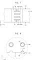
- FIG. 7 is a front view illustrating the through-groove test terminal in FIG. 5 .
- a module substrate 100 includes a wiring substrate and a through-groove test terminal 312 provided in an inner wall of a through groove 120 of the wiring substrate.
- the through-groove test terminal 312 includes at least one contact pad provided in the inner wall of the through groove 120.
- the module substrate 100 may be interchangeably referred to as the wiring substrate.
- the wiring substrate may include a plurality of stacked insulation layers and conductive patterns provided in the insulation layers, respectively.
- first to fifth insulation layers 110a, 110b, 110c, 110d, 110e may be sequentially stacked on one another.
- the first insulation layer 110a may be a lower cover insulation layer
- the second insulation layer 110b may be a lower insulation layer
- the third insulation layer 110c may be a core layer
- the fourth insulation layer 110d may be an upper insulation layer
- the fifth insulation layer 110e may be an upper cover insulation layer.
- the insulation layer may include an insulating material having a thermosetting resin such as epoxy resin or a thermoplastic resin such as polyimide.
- the insulation layer may include a resin impregnated in a core material such as organic fiber (glass fiber), for example, a prepreg, FR-4, or BT (Bismaleimide Triazine).
- a first conductive pattern 310a may be formed on a lower surface of the second insulation layer 110b, and a second conductive pattern 310b may be formed on an upper surface of the second insulation layer 110b.
- a third conductive pattern 3 10c may be formed on a lower surface of the fourth insulation layer 110d, and a fourth conductive pattern 310d may be formed on an upper surface of the fourth insulation layer 110d.
- the conductive pattern may include a metal material such as copper or aluminum.
- At least one through groove 120 is provided in a first sidewall S1 of the module substrate 100.
- the through groove 120 extends in a thickness direction of the module substrate 100, that is, in the stacking direction of the insulation layers (eg Z direction).
- the through groove 120 has a shape recessed from the first sidewall S1 to the inside.
- the through groove 120 may have a semi-circle or semi-elliptical shape or a trapezoidal shape when viewed in plan view.
- the first to fifth insulation layers 110a, 110b, 110c, 110d, 110e may have first to fifth semicircular holes 120a, 120b, 120c, 120d, 120e provided in sidewalls thereof, respectively.
- the through groove 120 may include the first to fifth semicircular holes 120a, 120b, 120c, 120d, 120e.
- the first conductive pattern 310a may be provided on the lower surface of the second insulation layer 110b to extend toward the inner wall of the through groove 120 in the second direction, and an end portion of the first conductive pattern 310a may be exposed from the inner wall of the through groove 120.
- the end portion of the first conductive pattern 310a exposed from the inner wall of the through groove 120 may be referred to as a first contact pad 312a.
- the first contact pad 312a may be formed integrally with the first conductive pattern 310a.
- a width of the first contact pad 312a may be greater than a width of the first conductive pattern 310a (e.g., a width of a portion other than the end portion of the first conductive pattern 310a). In this case, the first contact pad 312a may extend by a desired (or alternatively, predetermined) length along the inner wall of the second semicircular hole 120b.
- the second conductive pattern 310b may be provided on the upper surface of the second insulation layer 110b to extend toward the inner wall of the through groove 120 in the second direction, and an end portion of the second conductive pattern 310b may be exposed from the inner wall of the through groove 120.
- the end portion of the second conductive pattern 310b exposed from the inner wall of the through groove 120 may be referred to as a second contact pad 312b.
- the second contact pad 312b may be formed integrally with the second conductive pattern 310b.
- a width of the second contact pad 312b may be greater than a width of the second conductive pattern 310b (e.g., a width of a portion other than the end portion of the second conductive pattern 310b).
- the second contact pad 312b may extend by a desired (or alternatively, predetermined) length along the inner wall of the second semicircular hole 120b.
- the third conductive pattern 310c may be provided on the lower surface of the fourth insulation layer 110d to extend toward the inner wall of the through groove 120 in the second direction, and an end portion of the third conductive pattern 310c may be exposed from the inner wall of the through groove 120.
- the end portion of the third conductive pattern 310c exposed from the inner wall of the through groove 120 may be referred to as a third contact pad 312c.
- the third contact pad 312c may be formed integrally with the third conductive pattern 310c.
- a width of the third contact pad 312c may be greater than a width of the third conductive pattern 310c (e.g., a width of a portion other than the end portion of the third conductive pattern 310c).
- the third contact pad 312c may extend by a desired (or alternatively, predetermined) length along the inner wall of the fourth semicircular hole 120d.
- the fourth conductive pattern 310d may be provided on the upper surface of the fourth insulation layer 110d to extend toward the inner wall of the through groove 120 in the second direction, and an end portion of the fourth conductive pattern 310d may be exposed from the inner wall of the through groove 120.
- the end portion of the fourth conductive pattern 310d exposed from the inner wall of the through groove 120 may be referred to as a fourth contact pad 312d.
- the fourth contact pad 312d may be formed integrally with the fourth conductive pattern 310d.
- a width V of the fourth contact pad 312d may be greater than a width W of the fourth conductive pattern 310d (e.g., a width of a portion other than the end portion of the fourth conductive pattern 310d).
- the fourth contact pad 312d may extend by a desired (or alternatively, predetermined) length V along the inner wall of the fourth semicircular hole 120d.
- the through-groove test terminal 312 may include the first to fourth contact pads 312a, 312b, 312c, 312d, a surface of each of which is exposed from the inner wall of the through groove 120.
- the first to fourth contact pads 312a, 312b, 312c, 312d may be spaced apart from each other in the stacking direction.
- a e.g. pogo pin of a tester may be inserted into the through groove 120 to simultaneously contact the first to fourth contact pads 312a, 312b, 312c, 312d.
- the first to fourth conductive patterns 310a, 310b, 310c, 310d may be connected to one via 324.
- the via 324 may be electrically connected to a semiconductor device 200 through a signal line 311. Accordingly, the through-groove test terminal 312 may be electrically connected to the semiconductor device 200 by the via 324 and the signal line 311.
- the through-groove test terminal 312 may be spaced apart by a desired (or alternatively, predetermined) distance D1 from a vertical plane M extending from the first sidewall S1.
- the exposed surfaces of the first to fourth contact pads 312a, 312b, 312c, 312d may be spaced apart from the vertical plane M by the desired (or alternatively, predetermined) distance D1.
- a distance between both end portions of the inner wall of the through groove 120 in contact with the first sidewall S1, that is, a diameter D of the through groove 120 may be within a range of 200 ⁇ m to 800 ⁇ m.
- the spacing distance between the contact pads and the vertical plane M may be within a range of 80 ⁇ m to 320 ⁇ m.
- the through-groove test terminal 312 may be spaced apart by a desired (or alternatively, predetermined) distance D2 from each or either one of first and second horizontal planes N1, N2, the first horizontal plane N1 being a plane extending from the upper surface 102 of the wiring substrate and the second horizontal plane N2 being a plane extending from the lower surface 104 of the wiring substrate.
- the exposed surface of the first contact pad 312a may be spaced apart from the first horizontal plane N1 by the desired (or alternatively, predetermined) distance D2.
- the exposed surface of the fourth contact pad 312d may be spaced apart from the second horizontal plane N2 by the desired (or alternatively, predetermined) distance D2.
- a thickness of the wiring substrate may be within a range of 400 ⁇ m to 1,600 ⁇ m, and the distance between the first contact pad 312a and the first horizontal plane N1 and the distance between the fourth contact pad 312d and the second horizontal plane N2 may be within a range of 50 ⁇ m to 200 ⁇ m.
- the through-groove test terminal 312 may occupy a portion of the inner wall area of the through groove 120.
- the exposed surfaces of the first to fourth contact pads 312a, 312b, 312c, 312d may occupy at least 20% of the inner wall area of the through groove 120.
- the semiconductor module 10 may include a module substrate 100 and a semiconductor device 200 mounted on the module substrate 100.
- the module substrate 100 may include the wiring substrate having the at least one through groove 120 in the sidewall thereof and extending in the thickness direction thereof and the through-groove test terminal 312 having the at least one contact pad exposed from the inner wall of the through groove 120.
- the through-groove test terminal 312 may include the first to fourth contact pads 312a, 312b, 312c, 312d which are provided on the inner wall of the through groove 120 to be spaced apart from each other in the thickness direction of the wiring substrate.
- the through-groove test terminal 312 may be spaced apart by the desired (or alternatively, predetermined) distance D1 from the vertical plane M extending from the first sidewall S1.
- the through-groove test terminal 312 may be spaced apart by the desired (or alternatively, predetermined) distance D2 from the first and second horizontal planes N1 and N2 extending from the upper surface 102 and the lower surface 104 of the wiring substrate.
- interface signal connection terminals for inspection of a semiconductor device may be arranged in the sidewall of the wiring substrate having a small or micro form factor, thereby securing a design space for debug pads. Additionally or alternatively, because in some embodiments copper contact pads are not exposed from the sidewalls of the wiring substrate, it may be possible to improve contact reliability with the inspection e.g. pogo pin while satisfying PCB design regulations.
- FIG. 8 is a plan view illustrating a portion of an inspection pad portion of a memory module in accordance with some example embodiments.
- FIG. 9 is a cross-sectional view taken along the line B-B' in FIG. 8 .
- FIG. 10 is a perspective view illustrating a through-groove test terminal of the inspection pad portion in FIG. 8 .
- FIG. 11 is a plan view illustrating a fourth contact pad and a plating pattern of the through-groove test terminal in FIG. 10 .
- FIG. 12 is a front view illustrating the through-groove test terminal in FIG. 10 .
- the through-groove test terminal may be the same as or substantially similar to the through-groove test terminal described with reference to FIGS. 3 to 7 except for a configuration of an additional plating pattern.
- same reference numerals will be used to refer to the same or like elements and any further repetitive explanation concerning the above elements will be omitted.
- a through-groove test terminal includes at least one contact pad provided in an inner wall of a through groove 120 and a plating pattern 314 on the inner wall of the through groove 120 to cover the contact pad.
- the plating pattern 314 is provided on the inner wall of the through groove 120 and extends by a desired (or alternatively, predetermined) length in a thickness direction (eg Z direction) of a wiring substrate.
- the plating pattern 314 may make contact with exposed surfaces of first to fourth contact pads 312a, 312b, 312c, 312d.
- the plating pattern 314 may cover the exposed surfaces of the first to fourth contact pads 312a, 312b, 312c, 312d and portions of surfaces of second to fourth insulation layers 110b, 110c, 110d therebetween.
- the plating pattern 314 may be electrically connected to first to fourth conductive patterns 310a, 310b, 310c, 310d by the first to fourth contact pads 312a, 312b, 312c, 312d.
- the first to fourth conductive patterns 310a, 310b, 310c, 310d may be connected to one via 324. Accordingly, the through-groove test terminal may be electrically connected to a semiconductor device 200 by the via 324 and a signal line 311.
- a plating layer may be formed on the inner wall of the through groove 120 by an electroplating process, and then the plating layer may be patterned eg by an etching process or a drilling process to form the plating pattern 314.
- the plating pattern may include a metal material such as copper or nickel.
- the plating pattern 314 is spaced apart by a desired (or alternatively, predetermined) distance D3 from a vertical plane M extending from a first sidewall S1.
- the plating pattern 314 has a central angle ⁇ with respect to the center of the through groove 120.
- the central angle ⁇ has an angular range of 30 degrees to 70 degrees.
- a distance between both end portions of the inner wall of the through groove 120 in contact with the first sidewall S1, that is, a diameter D of the through groove 120 may be within a range of 200 ⁇ m to 800 ⁇ m.
- the spacing distance between the plating pattern and the vertical plane M may be within a range of 60 ⁇ m to 300 ⁇ m.
- the plating pattern 314 may be spaced apart by a desired (or alternatively, predetermined) distance D4 from each or either one of first and second horizontal planes N1, N2, the first horizontal plane N1 being a plane extending from an upper surface 102 of the wiring substrate and the second horizontal plane N2 being a plane extending from a lower surface 104 of the wiring substrate.
- a lower surface of the plating pattern 314 may be spaced apart from the first horizontal plane N1 by the distance D4.
- An upper surface of the plating pattern 314 may be spaced apart from the second horizontal plane N2 by the desired (or alternatively, predetermined) distance D4.
- a thickness of the wiring substrate may be within a range of 400 ⁇ m to 1,600 ⁇ m, and/or the distance between the lower surface of the plating pattern 314 and the first horizontal plane N1 and the distance between the upper surface of the plating pattern 314 and the second horizontal plane N2 may be within a range of 50 ⁇ m to 200 ⁇ m.
- the plating pattern 314 occupies a portion of the inner wall area of the through groove 120.
- the plating pattern 314 may occupy at least 40% of the inner wall area of the through groove 120.
- FIG. 13 is a cross-sectional view illustrating a through groove test terminal formed in a wiring substrate in accordance with some example embodiments.
- a through-groove test terminal may include first to fourth contact pads 312a, 312b, 312c, 312d exposed from an inner wall of a through groove 120, and the first to fourth contact pads 312a,312b, 312c, 312d may be connected to first to fourth conductive patterns 310a, 310b, 310c, 310d, respectively.
- the first and second conductive patterns 310a, 310b may be connected to a first via 324a, and the first via 324a may be electrically connected to a semiconductor device 200 through a first signal line 311a.
- the third and fourth conducive patterns 310c, 310d may be connected to a second via 324b, and the second via 324b may be electrically connected to the semiconductor device 200 through a second signal line 311b.
- first and second vias 324a, 324b may include a blind via or a buried via.
- an inspection mode or operation mode may be controlled according to an internal signal connection state of the first to fourth contact pads.
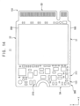
- FIG. 14 is a plan view illustrating a memory module in accordance with some example embodiments.
- the memory module may be the same as or substantially similar to the memory module described with reference to FIG. 1 except for a configuration of an inspection pad portion.
- same reference numerals will be used to refer to the same or like elements and any further repetitive explanation concerning the above elements will be omitted.
- an inspection pad portion 300 of a memory module 11 may be provided in a through groove 120 formed in at least one inner wall of a module substrate 100.
- the inspection pad portion 300 may include through-groove test terminals 312 provided in the through grooves 120, respectively.
- the through-groove test terminal may be the same as or substantially similar to the through-groove test terminal described with reference to FIGS. 3 to 7 .
- test terminals of the inspection pad portion 300 may be provided only in the through grooves 120 formed in the inner wall of a wiring substrate.
- the through grooves 120 may be formed in a first sidewall S1 to be spaced apart from each other along a first direction (eg X direction).
- the through-groove test terminals may be provided on inner walls of the through grooves 120, respectively.
- the inspection pad portion may include 10 through-groove test terminals. However, arrangements and the number of the through-groove test terminals may not be limited thereto.
- test pads are provided only on the sidewalls of the wiring substrate, a design space for electronic components and interface signal connection pads may be secured sufficiently.
- Memory modules according to some example embodiments have been described as being applied to an SSD, but it may not be limited thereto, and the memory module may be implemented as a semiconductor module including a plurality of memory devices.
- the host (or the host system) and the memory module disclosed in the present disclosure may be implemented as processing circuitry such as hardware including logic circuits or a combination of hardware and software such as a processor executing software.
- the processing circuitry may include, but is not limited to, a central processing unit (CPU) , an arithmetic logic unit (ALU), a digital signal processor, a microcomputer, a field programmable gate array (FPGA), a System-on-Chip (SoC), a programmable logic unit, a microprocessor, application-specific integrated circuit (ASIC), etc.
Landscapes
- Engineering & Computer Science (AREA)
- Microelectronics & Electronic Packaging (AREA)
- Manufacturing & Machinery (AREA)
- Printing Elements For Providing Electric Connections Between Printed Circuits (AREA)
Description
- Example embodiments relate to module substrates and/or semiconductor modules including the same. More particularly, example embodiments relate to module substrates for a memory module such as a solid state drive (SSD) and/or semiconductor modules including the same.
- A memory module such as a card-type SSD may be connected to a host system through a connector. A module substrate for the memory module may include test terminals as debugging pads. However, when the number of electronic components disposed on the module substrate increases and the module substrate has a small form factor, it may be difficult to secure a design space for the test terminals and to satisfy design regulations.
-
WO 2018/165538 A1 (TAG CONNECT LLC [US]) describes a side-edged connector system for accessing modules or printed circuit boards to allow the surface area of a PCB to be increased for the mounting of electrical components.US 10 791 632 B1 -
Clams - According to some example embodiments, a module substrate for a semiconductor module may include a wiring substrate including first to fifth insulation layers and first to fourth conductive patterns between the first to fifth insulation layers, the wiring substrate having at least one through groove, the through groove in at least one sidewall of the wiring substrate and extending in a stacking direction of the first to fifth insulation layers, and a through-groove test terminal including first to fourth contact pads, the first to fourth contact pads electrically connected to the first to fourth conductive patterns, respectively, surfaces of the first to fourth contact pads being exposed from an inner wall of the through groove. The first to fourth contact pads may be spaced apart from a vertical plane extending from the sidewall of the wiring substrate. A first distance between both end portions of the inner wall of the through groove that are in contact with the sidewall of the wiring substrate is within a range of 200 µm to 800 µm, and a second distance between each of the first to fourth contact pads and the vertical plane is within a range of 80 µm to 320 µm.
- According to some example embodiments, a semiconductor module may include a wiring substrate including a plurality of insulation layers and conductive patterns on the insulation layers, respectively, the wiring substrate having at least one through groove in at least one sidewall and extending in a stacking direction of the insulation layers, a semiconductor device on an upper surface or a lower surface of the wiring substrate, and a through-groove test terminal electrically connected to the conducive patterns for electrically inspecting the semiconductor device, the through-groove test terminal including a plurality of contact pads, surfaces of the contact pads being exposed from an inner wall of the through groove. The exposed surfaces of the contact pads may be arranged along the inner wall of the through groove and may be spaced apart from a vertical plane extending from the sidewall of the wiring substrate.
- According to some example embodiments, a semiconductor module may include a module substrate and a semiconductor device on the module substrate. The module substrate may include a wiring substrate having at least one through groove in a sidewall and extending in a thickness direction and a through-groove test terminal having at least one contact pad exposed from an inner wall of the through groove.
- The through-groove test terminal may include a plurality of contact pads on the inner wall of the through groove and spaced apart from each other in the thickness direction. The through-groove test terminal may be spaced apart by a distance from a vertical plane extending from the sidewall of the wiring substrate. The through-groove test terminal may be spaced apart by a distance from a horizontal plane extending from an upper surface or a lower surface of the wiring substrate.
- Accordingly, interface signal connection terminals for inspection of a semiconductor device may in some embodiments be arranged in a sidewall of a wiring substrate having a small or micro form factor, thereby securing a design space for debug pads. Additionally or alternatively, because copper contact pads are not exposed from a sidewall of the wiring substrate in some embodiments, it may be possible to improve contact reliability with an inspection pin, e.g., pogo pin, while satisfying PCB design regulations.
Merely for completeness, it is noted that in any embodiment a stacking direction may be the same direction as a thickness direction, wherein the same direction may be substantially parallel to a sidewall of the substrate and/or may cross a plane that is parallel to a substrate surface having devices mounted thereon. Furthermore, in any embodiment a 'vertical plane' may merely mean a plane that is parallel to and extending from a sidewall of the substrate and/or a 'horizontal plane' may merely mean a plan that extends from a substrate surface that is substantially perpendicular to the sidewall, so that the terms 'horizontal' and 'vertical' are relative terms and may not imply any absolute orientation. Similarly, the terms 'upper' and 'lower' are generally relative terms and may not imply any absolute orientation.
It is further noted that any dimension value provided herein such as in millimeters (mm) or micrometers (µm) may mean exactly or substantially the specified numeric value. For example, a reference to 10 µm may mean exactly or about 10 µm. - Some example embodiments will be more clearly understood from the following detailed description taken in conjunction with the accompanying drawings.
FIGS. 1 to 14 represent non-limiting, example embodiments as described herein. -
FIG. 1 is a plan view illustrating a memory module in accordance with an aspect not according to the invention. -
FIG. 2 is an enlarged perspective view illustrating portion 'I' inFIG. 1 . -
FIG. 3 is a plan view illustrating a portion of an inspection pad portion of a memory module in accordance with an aspect not according to the invention. -
FIG. 4 is a cross-sectional view taken along the line A-A' inFIG. 3 . -
FIG. 5 is a perspective view illustrating a through-groove test terminal of the inspection pad portion inFIG. 3 . -
FIG. 6 is a plan view illustrating a fourth contact pad of the through-groove test terminal inFIG. 5 . -
FIG. 7 is a front view illustrating the through-groove test terminal inFIG. 5 . -
FIG. 8 is a plan view illustrating a portion of an inspection pad portion of a memory module in accordance with some example embodiments. -
FIG. 9 is a cross-sectional view taken along the line B-B' inFIG. 8 . -
FIG. 10 is a perspective view illustrating a through-groove test terminal of the inspection pad portion inFIG. 8 . -
FIG. 11 is a plan view illustrating a fourth contact pad and a plating pattern of the through-groove test terminal inFIG. 10 . -
FIG. 12 is a front view illustrating the through-groove test terminal inFIG. 10 . -
FIG. 13 is a cross-sectional view illustrating a through groove test terminal formed in a wiring substrate in accordance with some example embodiments. -
FIG. 14 is a plan view illustrating a memory module in accordance with some example embodiments. - Some example embodiments provide module substrates capable of easily securing a design space for test pads.
- Some example embodiments provide semiconductor modules including the module substrate.
- Hereinafter, some example embodiments will be explained in detail with reference to the accompanying drawings.
-
FIG. 1 is a plan view illustrating a memory module in accordance with an aspect not according to the invention.FIG. 2 is an enlarged perspective view illustrating portion 'I' inFIG. 1 . - Referring to
FIGS. 1 and2 , amemory module 10 includes amodule substrate 100, asemiconductor device 200 mounted on themodule substrate 100 and aninspection pad portion 300 provided in a peripheral region of themodule substrate 100. Additionally, thememory module 10 may further includepassive devices 210 arranged on themodule substrate 100. - In some aspects, the
module substrate 100 may be a multi-layered circuit substrate having an upper surface and a lower surface opposite to each other. For example, themodule substrate 100 may be a printed circuit board (PCB). As described later, the PCB may include wirings on or in the surface thereof and vias connected to the wirings. The wirings may include conductive patterns for interconnecting with the semiconductor device and the passive devices. - The
module substrate 100 may extend in a first direction (eg X direction). Themodule substrate 100 may have a rectangular or square shape. Themodule substrate 100 may have a first sidewall S1 and a second sidewall S2 opposite to each other, a third sidewall S3 adjacent to the first sidewall S1 and a fourth sidewall S4 opposite to the third sidewall S3. Aconnector 150 having connection terminals for connection with a host system (not illustrated) may be provided in the third sidewall S3 of themodule substrate 100. - The
module substrate 100 may have a small or micro form factor (F/F) shape. Themodule substrate 100 may provide a 22×30 F/F design space. A length L1 of themodule substrate 100 in the first direction may be 30 mm, and/or a length L2 of themodule substrate 100 in a second direction (eg Y direction) may be 22 mm. However, it will be understood that the size of the module substrate is not limited thereto. - In some aspects, the
semiconductor device 200 may include a BGA type multi-chip package including eg an SSD controller, nonvolatile memory devices and/or buffer memory devices. Thesemiconductor device 200 may be mounted on themodule substrate 100 such that thememory module 10 is provided as solid state drive (SSD). The SSD may be used to replace a hard disk in a PC, notebook, etc. The SSD may be used in a mobile device such as smart phone, tablet PC, digital camera, MP3 player, or PDA. - The SSD controller may communicate a signal with the host using a host interface. The host interface may include a universal serial bus (USB), a small computer system interface (SCSI), a PCI express, an ATA, a parallel ATA, a serial ATA, a serial attached SCSI, etc. In here, the signal communicated between the SSD controller and the host may include a command, an address, data, etc. The SSD controller may analyze and process the signal inputted from the host.
- A plurality of the non-volatile memory devices may be used as a storage medium of the SSD. For example, the non-volatile memory device may include NAND flash memories. The non-volatile memory devices may be connected to the SSD controller through at least one channel CH. The SSD may use non-volatile memories such as PRAM, MRAM, ReRAM, or FRAM as a storage medium in place of flash memory.
- The buffer memory device may be used as a buffer area temporarily storing data received from the host or temporarily storing data read from the non-volatile memory devices. Additionally or alternatively, the buffer memory device may be used to drive software S/W used for an effective management of the non-volatile memory devices. Further, the buffer memory device may be used to store meta data received from the host and/or may be used to store cache data.
- For example, the buffer memory device may include at least one DRAM chip. The SSD may be embodied by replacing the DRAM with volatile memories (e.g., SRAM) or non-volatile memories (e.g., flash memory, FRAM, MRAM, ReRAM, or FRAM).
- In some aspects, the passive devices may be arranged on the upper surface or the lower surface of the
module substrate 100. The passive devices may include eg an inductor, a capacitor and/or a register, etc. - The
memory module 10 may further include a power management IC (PMIC) for adjusting a power applied to the semiconductor device. - The
inspection pad portion 300 includestest terminals module substrate 100 to electrically test thesemiconductor device 200. The test terminals may be electrically connected to thesemiconductor device 200 by wirings such as signal lines. Thesemiconductor device 200 may be electrically tested by connecting the test terminal to a test pin, e.g. pogo pin, which is a connection terminal of a tester (not illustrated). - For example, the
inspection pad portion 300 may include 12test terminals 312, 322 (2×6 Pin). Theinspection pad portion 300 may include eg two through-groove test terminals 312 and eg ten via-hole test terminals 322. In this case, the connection terminal of the tester may include 12 pogo pins corresponding to the test terminals. Thetest terminals inspection pad portion 300 may be used to debug a firmware code of thesemiconductor device 200. For example, in development and mass production stages of SSD products, a test task may be performed using thetest terminals semiconductor device 200. - As described later, the through-
groove test terminal 312 is provided to be exposed to an inner wall of a throughgroove 120 which is formed in the first sidewall S1 of themodule substrate 100. The via-hole test terminal 322 may be formed on an inner wall of a viahole 122 which penetrates themodule substrate 100. The via-hole test terminal 322 may include a through hole via. - Hereinafter, the through-groove test terminal of the inspection pad portion will be explained.
-
FIG. 3 is a plan view illustrating a portion of an inspection pad portion of a memory module in accordance with an aspect not according to the invention.FIG. 4 is a cross-sectional view taken along the line A-A' inFIG. 3 .FIG. 5 is a perspective view illustrating a through-groove test terminal of the inspection pad portion inFIG. 3 .FIG. 6 is a plan view illustrating a fourth contact pad of the through-groove test terminal inFIG. 5 .FIG. 7 is a front view illustrating the through-groove test terminal inFIG. 5 . - Referring to
FIGS. 3 to 7 , amodule substrate 100 includes a wiring substrate and a through-groove test terminal 312 provided in an inner wall of a throughgroove 120 of the wiring substrate. The through-groove test terminal 312 includes at least one contact pad provided in the inner wall of the throughgroove 120. Throughout this disclosure, themodule substrate 100 may be interchangeably referred to as the wiring substrate. - In some aspects, the wiring substrate may include a plurality of stacked insulation layers and conductive patterns provided in the insulation layers, respectively.
- For example, first to
fifth insulation layers first insulation layer 110a may be a lower cover insulation layer, thesecond insulation layer 110b may be a lower insulation layer, thethird insulation layer 110c may be a core layer, thefourth insulation layer 110d may be an upper insulation layer, and/or thefifth insulation layer 110e may be an upper cover insulation layer. - For example, the insulation layer may include an insulating material having a thermosetting resin such as epoxy resin or a thermoplastic resin such as polyimide. The insulation layer may include a resin impregnated in a core material such as organic fiber (glass fiber), for example, a prepreg, FR-4, or BT (Bismaleimide Triazine).
- A first
conductive pattern 310a may be formed on a lower surface of thesecond insulation layer 110b, and a secondconductive pattern 310b may be formed on an upper surface of thesecond insulation layer 110b. A thirdconductive pattern 3 10c may be formed on a lower surface of thefourth insulation layer 110d, and a fourthconductive pattern 310d may be formed on an upper surface of thefourth insulation layer 110d. For example, the conductive pattern may include a metal material such as copper or aluminum. - It will be understood that arrangements and numbers of the insulation layers and the conductive patterns are merely for example, and are not limited thereto.
- At least one through
groove 120 is provided in a first sidewall S1 of themodule substrate 100. The throughgroove 120 extends in a thickness direction of themodule substrate 100, that is, in the stacking direction of the insulation layers (eg Z direction). When viewed in plan view, the throughgroove 120 has a shape recessed from the first sidewall S1 to the inside. For example, the throughgroove 120 may have a semi-circle or semi-elliptical shape or a trapezoidal shape when viewed in plan view. - As illustrated in
FIGS. 4 and5 , the first tofifth insulation layers semicircular holes groove 120 may include the first to fifthsemicircular holes - The first
conductive pattern 310a may be provided on the lower surface of thesecond insulation layer 110b to extend toward the inner wall of the throughgroove 120 in the second direction, and an end portion of the firstconductive pattern 310a may be exposed from the inner wall of the throughgroove 120. The end portion of the firstconductive pattern 310a exposed from the inner wall of the throughgroove 120 may be referred to as afirst contact pad 312a. Thefirst contact pad 312a may be formed integrally with the firstconductive pattern 310a. A width of thefirst contact pad 312a may be greater than a width of the firstconductive pattern 310a (e.g., a width of a portion other than the end portion of the firstconductive pattern 310a). In this case, thefirst contact pad 312a may extend by a desired (or alternatively, predetermined) length along the inner wall of the secondsemicircular hole 120b. - The second
conductive pattern 310b may be provided on the upper surface of thesecond insulation layer 110b to extend toward the inner wall of the throughgroove 120 in the second direction, and an end portion of the secondconductive pattern 310b may be exposed from the inner wall of the throughgroove 120. The end portion of the secondconductive pattern 310b exposed from the inner wall of the throughgroove 120 may be referred to as asecond contact pad 312b. Thesecond contact pad 312b may be formed integrally with the secondconductive pattern 310b. A width of thesecond contact pad 312b may be greater than a width of the secondconductive pattern 310b (e.g., a width of a portion other than the end portion of the secondconductive pattern 310b). In this case, thesecond contact pad 312b may extend by a desired (or alternatively, predetermined) length along the inner wall of the secondsemicircular hole 120b. - The third
conductive pattern 310c may be provided on the lower surface of thefourth insulation layer 110d to extend toward the inner wall of the throughgroove 120 in the second direction, and an end portion of the thirdconductive pattern 310c may be exposed from the inner wall of the throughgroove 120. The end portion of the thirdconductive pattern 310c exposed from the inner wall of the throughgroove 120 may be referred to as athird contact pad 312c. Thethird contact pad 312c may be formed integrally with the thirdconductive pattern 310c. A width of thethird contact pad 312c may be greater than a width of the thirdconductive pattern 310c (e.g., a width of a portion other than the end portion of the thirdconductive pattern 310c). In this case, thethird contact pad 312c may extend by a desired (or alternatively, predetermined) length along the inner wall of the fourthsemicircular hole 120d. - The fourth
conductive pattern 310d may be provided on the upper surface of thefourth insulation layer 110d to extend toward the inner wall of the throughgroove 120 in the second direction, and an end portion of the fourthconductive pattern 310d may be exposed from the inner wall of the throughgroove 120. The end portion of the fourthconductive pattern 310d exposed from the inner wall of the throughgroove 120 may be referred to as afourth contact pad 312d. Thefourth contact pad 312d may be formed integrally with the fourthconductive pattern 310d. A width V of thefourth contact pad 312d may be greater than a width W of the fourthconductive pattern 310d (e.g., a width of a portion other than the end portion of the fourthconductive pattern 310d). In this case, thefourth contact pad 312d may extend by a desired (or alternatively, predetermined) length V along the inner wall of the fourthsemicircular hole 120d. - Accordingly, the through-
groove test terminal 312 may include the first tofourth contact pads groove 120. The first tofourth contact pads groove 120 to simultaneously contact the first tofourth contact pads - The first to fourth
conductive patterns semiconductor device 200 through asignal line 311. Accordingly, the through-groove test terminal 312 may be electrically connected to thesemiconductor device 200 by the via 324 and thesignal line 311. - As illustrated in
FIGS. 6 and7 , the through-groove test terminal 312 may be spaced apart by a desired (or alternatively, predetermined) distance D1 from a vertical plane M extending from the first sidewall S1. The exposed surfaces of the first tofourth contact pads - For example, a distance between both end portions of the inner wall of the through
groove 120 in contact with the first sidewall S1, that is, a diameter D of the throughgroove 120 may be within a range of 200 µm to 800 µm. The spacing distance between the contact pads and the vertical plane M may be within a range of 80 µm to 320 µm. - Further, the through-
groove test terminal 312 may be spaced apart by a desired (or alternatively, predetermined) distance D2 from each or either one of first and second horizontal planes N1, N2, the first horizontal plane N1 being a plane extending from theupper surface 102 of the wiring substrate and the second horizontal plane N2 being a plane extending from thelower surface 104 of the wiring substrate. The exposed surface of thefirst contact pad 312a may be spaced apart from the first horizontal plane N1 by the desired (or alternatively, predetermined) distance D2. The exposed surface of thefourth contact pad 312d may be spaced apart from the second horizontal plane N2 by the desired (or alternatively, predetermined) distance D2. - For example, a thickness of the wiring substrate may be within a range of 400 µm to 1,600 µm, and the distance between the
first contact pad 312a and the first horizontal plane N1 and the distance between thefourth contact pad 312d and the second horizontal plane N2 may be within a range of 50 µm to 200 µm. - The through-
groove test terminal 312 may occupy a portion of the inner wall area of the throughgroove 120. For example, the exposed surfaces of the first tofourth contact pads groove 120. - As described above, the
semiconductor module 10 may include amodule substrate 100 and asemiconductor device 200 mounted on themodule substrate 100. Themodule substrate 100 may include the wiring substrate having the at least one throughgroove 120 in the sidewall thereof and extending in the thickness direction thereof and the through-groove test terminal 312 having the at least one contact pad exposed from the inner wall of the throughgroove 120. - The through-
groove test terminal 312 may include the first tofourth contact pads groove 120 to be spaced apart from each other in the thickness direction of the wiring substrate. The through-groove test terminal 312 may be spaced apart by the desired (or alternatively, predetermined) distance D1 from the vertical plane M extending from the first sidewall S1. The through-groove test terminal 312 may be spaced apart by the desired (or alternatively, predetermined) distance D2 from the first and second horizontal planes N1 and N2 extending from theupper surface 102 and thelower surface 104 of the wiring substrate. - Accordingly, in some aspects interface signal connection terminals for inspection of a semiconductor device may be arranged in the sidewall of the wiring substrate having a small or micro form factor, thereby securing a design space for debug pads. Additionally or alternatively, because in some embodiments copper contact pads are not exposed from the sidewalls of the wiring substrate, it may be possible to improve contact reliability with the inspection e.g. pogo pin while satisfying PCB design regulations.
-
FIG. 8 is a plan view illustrating a portion of an inspection pad portion of a memory module in accordance with some example embodiments.FIG. 9 is a cross-sectional view taken along the line B-B' inFIG. 8 .FIG. 10 is a perspective view illustrating a through-groove test terminal of the inspection pad portion inFIG. 8 .FIG. 11 is a plan view illustrating a fourth contact pad and a plating pattern of the through-groove test terminal inFIG. 10 .FIG. 12 is a front view illustrating the through-groove test terminal inFIG. 10 . The through-groove test terminal may be the same as or substantially similar to the through-groove test terminal described with reference toFIGS. 3 to 7 except for a configuration of an additional plating pattern. Thus, same reference numerals will be used to refer to the same or like elements and any further repetitive explanation concerning the above elements will be omitted. - Referring to
FIGS. 8 to 12 , a through-groove test terminal includes at least one contact pad provided in an inner wall of a throughgroove 120 and aplating pattern 314 on the inner wall of the throughgroove 120 to cover the contact pad. - In the invention, the
plating pattern 314 is provided on the inner wall of the throughgroove 120 and extends by a desired (or alternatively, predetermined) length in a thickness direction (eg Z direction) of a wiring substrate. - As illustrated in
FIGS. 9 and 10 , theplating pattern 314 may make contact with exposed surfaces of first tofourth contact pads plating pattern 314 may cover the exposed surfaces of the first tofourth contact pads - The
plating pattern 314 may be electrically connected to first to fourthconductive patterns fourth contact pads conductive patterns semiconductor device 200 by the via 324 and asignal line 311. - A plating layer may be formed on the inner wall of the through
groove 120 by an electroplating process, and then the plating layer may be patterned eg by an etching process or a drilling process to form theplating pattern 314. For example, the plating pattern may include a metal material such as copper or nickel. - As illustrated in
FIGS. 11 and 12 , theplating pattern 314 is spaced apart by a desired (or alternatively, predetermined) distance D3 from a vertical plane M extending from a first sidewall S1. Theplating pattern 314 has a central angle θ with respect to the center of the throughgroove 120. The central angle θ has an angular range of 30 degrees to 70 degrees. - For example, a distance between both end portions of the inner wall of the through
groove 120 in contact with the first sidewall S1, that is, a diameter D of the throughgroove 120 may be within a range of 200 µm to 800 µm. The spacing distance between the plating pattern and the vertical plane M may be within a range of 60 µm to 300 µm. - Further, the
plating pattern 314 may be spaced apart by a desired (or alternatively, predetermined) distance D4 from each or either one of first and second horizontal planes N1, N2, the first horizontal plane N1 being a plane extending from anupper surface 102 of the wiring substrate and the second horizontal plane N2 being a plane extending from alower surface 104 of the wiring substrate. A lower surface of theplating pattern 314 may be spaced apart from the first horizontal plane N1 by the distance D4. An upper surface of theplating pattern 314 may be spaced apart from the second horizontal plane N2 by the desired (or alternatively, predetermined) distance D4. - For example, a thickness of the wiring substrate may be within a range of 400 µm to 1,600 µm, and/or the distance between the lower surface of the
plating pattern 314 and the first horizontal plane N1 and the distance between the upper surface of theplating pattern 314 and the second horizontal plane N2 may be within a range of 50 µm to 200 µm. - The
plating pattern 314 occupies a portion of the inner wall area of the throughgroove 120. For example, theplating pattern 314 may occupy at least 40% of the inner wall area of the throughgroove 120. -
FIG. 13 is a cross-sectional view illustrating a through groove test terminal formed in a wiring substrate in accordance with some example embodiments. - Referring to
FIG. 13 , a through-groove test terminal may include first tofourth contact pads groove 120, and the first tofourth contact pads conductive patterns - In some example embodiments, the first and second
conductive patterns semiconductor device 200 through afirst signal line 311a. The third and fourthconducive patterns semiconductor device 200 through asecond signal line 311b. - For example, the first and
second vias - Accordingly, when a pogo pin of a tester is inserted into the through
groove 120 to contact the first tofourth contact pads -
FIG. 14 is a plan view illustrating a memory module in accordance with some example embodiments. The memory module may be the same as or substantially similar to the memory module described with reference toFIG. 1 except for a configuration of an inspection pad portion. Thus, same reference numerals will be used to refer to the same or like elements and any further repetitive explanation concerning the above elements will be omitted. - Referring to
FIG. 14 , aninspection pad portion 300 of amemory module 11 may be provided in a throughgroove 120 formed in at least one inner wall of amodule substrate 100. Theinspection pad portion 300 may include through-groove test terminals 312 provided in the throughgrooves 120, respectively. The through-groove test terminal may be the same as or substantially similar to the through-groove test terminal described with reference toFIGS. 3 to 7 . - In some example embodiments, the test terminals of the
inspection pad portion 300 may be provided only in the throughgrooves 120 formed in the inner wall of a wiring substrate. - For example, the through
grooves 120 may be formed in a first sidewall S1 to be spaced apart from each other along a first direction (eg X direction). The through-groove test terminals may be provided on inner walls of the throughgrooves 120, respectively. For example, the inspection pad portion may include 10 through-groove test terminals. However, arrangements and the number of the through-groove test terminals may not be limited thereto. - Thus, because in some embodiments the test pads are provided only on the sidewalls of the wiring substrate, a design space for electronic components and interface signal connection pads may be secured sufficiently.
- Memory modules according to some example embodiments have been described as being applied to an SSD, but it may not be limited thereto, and the memory module may be implemented as a semiconductor module including a plurality of memory devices.
- The host (or the host system) and the memory module disclosed in the present disclosure may be implemented as processing circuitry such as hardware including logic circuits or a combination of hardware and software such as a processor executing software. For example, the processing circuitry may include, but is not limited to, a central processing unit (CPU) , an arithmetic logic unit (ALU), a digital signal processor, a microcomputer, a field programmable gate array (FPGA), a System-on-Chip (SoC), a programmable logic unit, a microprocessor, application-specific integrated circuit (ASIC), etc.
- The foregoing is illustrative of some example embodiments and is not to be construed as limiting thereof. Although a few example embodiments have been described, those skilled in the art will readily appreciate that many modifications are possible in the disclosed example embodiments without materially departing from the novel teachings and advantages of the present inventive concepts. Accordingly, all such modifications to the disclosed example embodiments are intended to be included within the scope of the appended claims.
Claims (14)
- A module substrate (100) for a semiconductor module (10), comprising:a wiring substrate having an upper surface (102) and a lower surface (104) opposite to each other and including a wiring including at least one conductive pattern (310a, 310b, 310c, 310d) formed therein, the wiring substrate having at least one through groove (120) in at least one sidewall (S1) and extending in a thickness direction; anda through-groove test terminal (312) including at least one contact pad (312a, 312b, 312c, 312d), the at least one contact pad (312a, 312b, 312c, 312d) comprising an end portion of the at least one conductive pattern, and a surface of the contact pad (312a, 312b, 312c, 312d) being exposed from an inner wall of the through groove,wherein the contact pad is spaced apart from a vertical plane (M) extending from the sidewall of the wiring substrate, and characterized in that the through-groove test terminal (312) further includes a plating pattern (314) on the inner wall of the through groove, the plating pattern (314) configured to cover the exposed surface of the contact pad (312a, 312b, 312c, 312d) and being spaced apart from the vertical plane by a distance (D3), wherein the plating pattern forms an angle (θ) centered with respect to a center of the through groove, the angle (θ) having an angular range of 30 degrees to 70 degrees.
- The module substrate for the semiconductor module of claim 1, wherein the wiring substrate includes a plurality of stacked insulation layers (110a, 110b, 110c, 110d, 110e), a plurality of conductive patterns provided on the insulation layers, respectively, and a plurality of contact pads electrically connected to the conductive patterns, respectively.
- The module substrate for the semiconductor module of claim 2, wherein the contact pads are spaced apart from each other along a stacking direction of the insulation layers.
- The module substrate for the semiconductor module of claim 2 or 3, wherein a plurality of the contact pads occupies at least 20% of an area of the inner wall of the through groove.
- The module substrate for the semiconductor module of any preceding claim, wherein the contact pad comprises a plurality of contact pads, the contact pads electrically connected to a plurality of conductive patterns, respectively, and the plating pattern cover surfaces of the contact pads.
- The module substrate for the semiconductor module of any preceding claim, wherein the plating pattern occupies at least 40% of an area of the inner wall of the through groove.
- The module substrate for the semiconductor module of any preceding claim, wherein a first distance (D) between both end portions of the inner wall of the through groove in contact with the sidewall is within a range of 200 µm to 800 µm, and a second distance (D1) between the contact pad and the vertical plane is within a range of 80 µm to 320 µm.
- The module substrate for the semiconductor module of any preceding claim, wherein the contact pad is spaced apart from a horizontal plane (N1, N2), which extends from the upper surface or the lower surface of the wiring substrate, by a distance (D2).
- The module substrate for the semiconductor module of claim 8, wherein a thickness of the wiring substrate is within a range of 400 µm to 1,600 µm, and the distance between the contact pad and the horizontal plane is within a range of 50 µm to 200 µm.
- The module substrate for the semiconductor module of any preceding claim,wherein the wiring substrate includes first to fifth insulation layers and first to fourth conductive patterns between the first to fifth insulation layers, the through groove in the at least one sidewall of the wiring substrate extending in a stacking direction of the first to fifth insulation layers; andwherein the through-groove test terminal includes first to fourth contact pads, the first to fourth contact pads electrically connected to the first to fourth conductive patterns, respectively, surfaces of the first to fourth contact pads being exposed from an inner wall of the through groove,wherein the first to fourth contact pads are spaced apart from the vertical plane extending from the sidewall of the wiring substrate, andwherein a second distance between each of the first to fourth contact pads and the vertical plane is within a range of 80 µm to 320 µm.
- The module substrate for the semiconductor module of claim 10, wherein the through-groove test terminal further includes a plating pattern on the inner wall of the through groove, the plating pattern configured to cover the exposed surfaces of the first to fourth contact pads and being spaced apart from the vertical plane by a third distance.
- The module substrate for the semiconductor module of claim 10 or 11, wherein the first to fourth conductive patterns are connected to a via (324) that penetrates at least a portion of the wiring substrate.
- The module substrate for the semiconductor module of any one of claims 10 to 12, wherein some of the first to fourth conductive patterns are connected to a first via (324a) that penetrates at least a portion of the wiring substrate and others of the first to fourth conductive patterns are connected to a second via (324b) that penetrates another portion of the wiring substrate.
- The module substrate for the semiconductor module of any one of the preceding claims, wherein the at least one contact pad is formed integrally with the at least one conductive pattern.
Applications Claiming Priority (1)
| Application Number | Priority Date | Filing Date | Title |
|---|---|---|---|
| KR1020200135836A KR102867266B1 (en) | 2020-10-20 | 2020-10-20 | Module substrate and semiconductor module including the same |
Publications (2)
| Publication Number | Publication Date |
|---|---|
| EP3989683A1 EP3989683A1 (en) | 2022-04-27 |
| EP3989683B1 true EP3989683B1 (en) | 2023-09-20 |
Family
ID=77358083
Family Applications (1)
| Application Number | Title | Priority Date | Filing Date |
|---|---|---|---|
| EP21187443.3A Active EP3989683B1 (en) | 2020-10-20 | 2021-07-23 | Module substrate and semiconductor module including the same |
Country Status (4)
| Country | Link |
|---|---|
| US (2) | US11490509B2 (en) |
| EP (1) | EP3989683B1 (en) |
| KR (1) | KR102867266B1 (en) |
| CN (1) | CN114390768A (en) |
Family Cites Families (13)
| Publication number | Priority date | Publication date | Assignee | Title |
|---|---|---|---|---|
| JPH10247766A (en) | 1997-03-03 | 1998-09-14 | Alps Electric Co Ltd | Circuit board |
| JP2003338672A (en) | 2002-05-21 | 2003-11-28 | Daisho Denshi:Kk | Printed wiring board |
| JP2005223266A (en) | 2004-02-09 | 2005-08-18 | Sharp Corp | Substrate end face through hole manufacturing method |
| KR100654085B1 (en) | 2005-08-09 | 2006-12-06 | 주식회사 신화테크 | Slew-type through hole manufacturing method of multilayer printed circuit board |
| KR100723529B1 (en) * | 2006-05-10 | 2007-05-30 | 삼성전자주식회사 | Circuit board having a solder ball land having a hole and a semiconductor package having the same |
| JP4331769B2 (en) * | 2007-02-28 | 2009-09-16 | Tdk株式会社 | Wiring structure, method for forming the same, and printed wiring board |
| US7741709B2 (en) | 2008-01-09 | 2010-06-22 | Inpaq Technology Co., Ltd. | Embedded type multifunctional integrated structure for integrating protection components and method for manufacturing the same |
| KR20100041515A (en) | 2008-10-14 | 2010-04-22 | 삼성전자주식회사 | Method for testing a solid state drive having a removable auxiliary test terminals |
| JP2015053363A (en) | 2013-09-06 | 2015-03-19 | 京セラサーキットソリューションズ株式会社 | Method for manufacturing printed wiring board |
| JP6316609B2 (en) * | 2014-02-05 | 2018-04-25 | 新光電気工業株式会社 | WIRING BOARD, SEMICONDUCTOR DEVICE, WIRING BOARD MANUFACTURING METHOD, AND SEMICONDUCTOR DEVICE MANUFACTURING METHOD |
| KR20160018921A (en) * | 2014-08-07 | 2016-02-18 | 삼성전자주식회사 | Semiconductor Memory Device And Method of Fabricating The Same |
| US10535938B2 (en) * | 2017-03-10 | 2020-01-14 | Tag-Connet, Llc | Side-edge connector system providing electrical connection between devices in a manner which minimizes dedicated connection space |
| US10791632B1 (en) | 2019-09-20 | 2020-09-29 | Raytheon Company | Extremely low profile electrical interconnect for printed wiring board |
-
2020
- 2020-10-20 KR KR1020200135836A patent/KR102867266B1/en active Active
-
2021
- 2021-06-25 US US17/358,800 patent/US11490509B2/en active Active
- 2021-07-23 EP EP21187443.3A patent/EP3989683B1/en active Active
- 2021-09-24 CN CN202111124136.XA patent/CN114390768A/en active Pending
-
2022
- 2022-08-30 US US17/898,907 patent/US11792921B2/en active Active
Also Published As
| Publication number | Publication date |
|---|---|
| US11792921B2 (en) | 2023-10-17 |
| US11490509B2 (en) | 2022-11-01 |
| CN114390768A (en) | 2022-04-22 |
| EP3989683A1 (en) | 2022-04-27 |
| KR20220052011A (en) | 2022-04-27 |
| US20220124904A1 (en) | 2022-04-21 |
| KR102867266B1 (en) | 2025-10-01 |
| US20220418097A1 (en) | 2022-12-29 |
Similar Documents
| Publication | Publication Date | Title |
|---|---|---|
| US10204661B2 (en) | Semiconductor device | |
| US9768536B2 (en) | Socket with routed contacts | |
| US20060049512A1 (en) | Thin module system and method with skew reduction | |
| KR100834826B1 (en) | Integrated circuit module structure with reduced handling damage and terminal resistor arrangement method | |
| EP2973698B1 (en) | Method of manufacturing a stacked memory package and pinout design of ic package substrate | |
| US11277916B2 (en) | Memory system and storage device including printed circuit board with subset of channels arranged in point-to-point topology and subset of channels arranged in daisy-chain topology | |
| US9024426B2 (en) | Semiconductor device and method of manufacturing the same | |
| US12267957B2 (en) | Hybrid pitch through hole connector | |
| KR20130097481A (en) | Printed circuit board(pcb), and memory module comprising the same pcb | |
| US8093708B2 (en) | Semiconductor package having non-uniform contact arrangement | |
| US8422236B2 (en) | Pin module and chip on board type use device | |
| US20170109098A1 (en) | Semiconductor device | |
| US11792921B2 (en) | Module substrate and semiconductor module including the same | |
| US12295095B2 (en) | Printed circuit board and storage device including the same | |
| US9888565B2 (en) | Memory module and solid state drive having the same | |
| US10242716B2 (en) | Semiconductor device having a slit for aligning a connector and a hole for determining positional accuracy of the slit | |
| KR20100115268A (en) | Solid state drive | |
| US20170105282A1 (en) | Circuit board structure | |
| US9543271B2 (en) | Semiconductor device having a sealing layer covering a semiconductor memory unit and a memory controller | |
| US12463140B2 (en) | Flexible interposer for semiconductor dies | |
| KR102888554B1 (en) | Module substrate for semiconductor module, semiconductor module and test socket for testing the same | |
| US12520424B2 (en) | Semiconductor storage device | |
| US20250098068A1 (en) | Semiconductor storage device and semiconductor storage unit | |
| US20260114280A1 (en) | Memory device | |
| TWM657395U (en) | Circuit board assembly and host equipment |
Legal Events
| Date | Code | Title | Description |
|---|---|---|---|
| PUAI | Public reference made under article 153(3) epc to a published international application that has entered the european phase |
Free format text: ORIGINAL CODE: 0009012 |
|
| STAA | Information on the status of an ep patent application or granted ep patent |
Free format text: STATUS: REQUEST FOR EXAMINATION WAS MADE |
|
| 17P | Request for examination filed |
Effective date: 20210723 |
|
| AK | Designated contracting states |
Kind code of ref document: A1 Designated state(s): AL AT BE BG CH CY CZ DE DK EE ES FI FR GB GR HR HU IE IS IT LI LT LU LV MC MK MT NL NO PL PT RO RS SE SI SK SM TR |
|
| STAA | Information on the status of an ep patent application or granted ep patent |
Free format text: STATUS: EXAMINATION IS IN PROGRESS |
|
| 17Q | First examination report despatched |
Effective date: 20220913 |
|
| GRAP | Despatch of communication of intention to grant a patent |
Free format text: ORIGINAL CODE: EPIDOSNIGR1 |
|
| STAA | Information on the status of an ep patent application or granted ep patent |
Free format text: STATUS: GRANT OF PATENT IS INTENDED |
|
| RIC1 | Information provided on ipc code assigned before grant |
Ipc: H05K 3/42 20060101ALN20230323BHEP Ipc: H05K 1/11 20060101ALN20230323BHEP Ipc: H05K 3/40 20060101ALI20230323BHEP Ipc: H05K 1/02 20060101AFI20230323BHEP |
|
| INTG | Intention to grant announced |
Effective date: 20230404 |
|
| P01 | Opt-out of the competence of the unified patent court (upc) registered |
Effective date: 20230519 |
|
| GRAS | Grant fee paid |
Free format text: ORIGINAL CODE: EPIDOSNIGR3 |
|
| GRAA | (expected) grant |
Free format text: ORIGINAL CODE: 0009210 |
|
| STAA | Information on the status of an ep patent application or granted ep patent |
Free format text: STATUS: THE PATENT HAS BEEN GRANTED |
|
| AK | Designated contracting states |
Kind code of ref document: B1 Designated state(s): AL AT BE BG CH CY CZ DE DK EE ES FI FR GB GR HR HU IE IS IT LI LT LU LV MC MK MT NL NO PL PT RO RS SE SI SK SM TR |
|
| REG | Reference to a national code |
Ref country code: GB Ref legal event code: FG4D |
|
| REG | Reference to a national code |
Ref country code: CH Ref legal event code: EP |
|
| REG | Reference to a national code |
Ref country code: DE Ref legal event code: R096 Ref document number: 602021005247 Country of ref document: DE |
|
| REG | Reference to a national code |
Ref country code: IE Ref legal event code: FG4D |
|
| REG | Reference to a national code |
Ref country code: LT Ref legal event code: MG9D |
|
| PG25 | Lapsed in a contracting state [announced via postgrant information from national office to epo] |
Ref country code: GR Free format text: LAPSE BECAUSE OF FAILURE TO SUBMIT A TRANSLATION OF THE DESCRIPTION OR TO PAY THE FEE WITHIN THE PRESCRIBED TIME-LIMIT Effective date: 20231221 |
|
| REG | Reference to a national code |
Ref country code: NL Ref legal event code: MP Effective date: 20230920 |
|
| PG25 | Lapsed in a contracting state [announced via postgrant information from national office to epo] |
Ref country code: SE Free format text: LAPSE BECAUSE OF FAILURE TO SUBMIT A TRANSLATION OF THE DESCRIPTION OR TO PAY THE FEE WITHIN THE PRESCRIBED TIME-LIMIT Effective date: 20230920 Ref country code: RS Free format text: LAPSE BECAUSE OF FAILURE TO SUBMIT A TRANSLATION OF THE DESCRIPTION OR TO PAY THE FEE WITHIN THE PRESCRIBED TIME-LIMIT Effective date: 20230920 Ref country code: NO Free format text: LAPSE BECAUSE OF FAILURE TO SUBMIT A TRANSLATION OF THE DESCRIPTION OR TO PAY THE FEE WITHIN THE PRESCRIBED TIME-LIMIT Effective date: 20231220 Ref country code: LV Free format text: LAPSE BECAUSE OF FAILURE TO SUBMIT A TRANSLATION OF THE DESCRIPTION OR TO PAY THE FEE WITHIN THE PRESCRIBED TIME-LIMIT Effective date: 20230920 Ref country code: LT Free format text: LAPSE BECAUSE OF FAILURE TO SUBMIT A TRANSLATION OF THE DESCRIPTION OR TO PAY THE FEE WITHIN THE PRESCRIBED TIME-LIMIT Effective date: 20230920 Ref country code: HR Free format text: LAPSE BECAUSE OF FAILURE TO SUBMIT A TRANSLATION OF THE DESCRIPTION OR TO PAY THE FEE WITHIN THE PRESCRIBED TIME-LIMIT Effective date: 20230920 Ref country code: GR Free format text: LAPSE BECAUSE OF FAILURE TO SUBMIT A TRANSLATION OF THE DESCRIPTION OR TO PAY THE FEE WITHIN THE PRESCRIBED TIME-LIMIT Effective date: 20231221 Ref country code: FI Free format text: LAPSE BECAUSE OF FAILURE TO SUBMIT A TRANSLATION OF THE DESCRIPTION OR TO PAY THE FEE WITHIN THE PRESCRIBED TIME-LIMIT Effective date: 20230920 |
|
| REG | Reference to a national code |
Ref country code: AT Ref legal event code: MK05 Ref document number: 1614436 Country of ref document: AT Kind code of ref document: T Effective date: 20230920 |
|
| PG25 | Lapsed in a contracting state [announced via postgrant information from national office to epo] |
Ref country code: NL Free format text: LAPSE BECAUSE OF FAILURE TO SUBMIT A TRANSLATION OF THE DESCRIPTION OR TO PAY THE FEE WITHIN THE PRESCRIBED TIME-LIMIT Effective date: 20230920 |
|
| PG25 | Lapsed in a contracting state [announced via postgrant information from national office to epo] |
Ref country code: IS Free format text: LAPSE BECAUSE OF FAILURE TO SUBMIT A TRANSLATION OF THE DESCRIPTION OR TO PAY THE FEE WITHIN THE PRESCRIBED TIME-LIMIT Effective date: 20240120 |
|
| PG25 | Lapsed in a contracting state [announced via postgrant information from national office to epo] |
Ref country code: AT Free format text: LAPSE BECAUSE OF FAILURE TO SUBMIT A TRANSLATION OF THE DESCRIPTION OR TO PAY THE FEE WITHIN THE PRESCRIBED TIME-LIMIT Effective date: 20230920 |
|
| PG25 | Lapsed in a contracting state [announced via postgrant information from national office to epo] |
Ref country code: ES Free format text: LAPSE BECAUSE OF FAILURE TO SUBMIT A TRANSLATION OF THE DESCRIPTION OR TO PAY THE FEE WITHIN THE PRESCRIBED TIME-LIMIT Effective date: 20230920 |
|
| PG25 | Lapsed in a contracting state [announced via postgrant information from national office to epo] |
Ref country code: SM Free format text: LAPSE BECAUSE OF FAILURE TO SUBMIT A TRANSLATION OF THE DESCRIPTION OR TO PAY THE FEE WITHIN THE PRESCRIBED TIME-LIMIT Effective date: 20230920 Ref country code: RO Free format text: LAPSE BECAUSE OF FAILURE TO SUBMIT A TRANSLATION OF THE DESCRIPTION OR TO PAY THE FEE WITHIN THE PRESCRIBED TIME-LIMIT Effective date: 20230920 Ref country code: IS Free format text: LAPSE BECAUSE OF FAILURE TO SUBMIT A TRANSLATION OF THE DESCRIPTION OR TO PAY THE FEE WITHIN THE PRESCRIBED TIME-LIMIT Effective date: 20240120 Ref country code: ES Free format text: LAPSE BECAUSE OF FAILURE TO SUBMIT A TRANSLATION OF THE DESCRIPTION OR TO PAY THE FEE WITHIN THE PRESCRIBED TIME-LIMIT Effective date: 20230920 Ref country code: EE Free format text: LAPSE BECAUSE OF FAILURE TO SUBMIT A TRANSLATION OF THE DESCRIPTION OR TO PAY THE FEE WITHIN THE PRESCRIBED TIME-LIMIT Effective date: 20230920 Ref country code: CZ Free format text: LAPSE BECAUSE OF FAILURE TO SUBMIT A TRANSLATION OF THE DESCRIPTION OR TO PAY THE FEE WITHIN THE PRESCRIBED TIME-LIMIT Effective date: 20230920 Ref country code: AT Free format text: LAPSE BECAUSE OF FAILURE TO SUBMIT A TRANSLATION OF THE DESCRIPTION OR TO PAY THE FEE WITHIN THE PRESCRIBED TIME-LIMIT Effective date: 20230920 Ref country code: SK Free format text: LAPSE BECAUSE OF FAILURE TO SUBMIT A TRANSLATION OF THE DESCRIPTION OR TO PAY THE FEE WITHIN THE PRESCRIBED TIME-LIMIT Effective date: 20230920 Ref country code: PT Free format text: LAPSE BECAUSE OF FAILURE TO SUBMIT A TRANSLATION OF THE DESCRIPTION OR TO PAY THE FEE WITHIN THE PRESCRIBED TIME-LIMIT Effective date: 20240122 |
|
| PG25 | Lapsed in a contracting state [announced via postgrant information from national office to epo] |
Ref country code: PL Free format text: LAPSE BECAUSE OF FAILURE TO SUBMIT A TRANSLATION OF THE DESCRIPTION OR TO PAY THE FEE WITHIN THE PRESCRIBED TIME-LIMIT Effective date: 20230920 Ref country code: IT Free format text: LAPSE BECAUSE OF FAILURE TO SUBMIT A TRANSLATION OF THE DESCRIPTION OR TO PAY THE FEE WITHIN THE PRESCRIBED TIME-LIMIT Effective date: 20230920 |
|
| REG | Reference to a national code |
Ref country code: DE Ref legal event code: R097 Ref document number: 602021005247 Country of ref document: DE |
|
| PG25 | Lapsed in a contracting state [announced via postgrant information from national office to epo] |
Ref country code: DK Free format text: LAPSE BECAUSE OF FAILURE TO SUBMIT A TRANSLATION OF THE DESCRIPTION OR TO PAY THE FEE WITHIN THE PRESCRIBED TIME-LIMIT Effective date: 20230920 |
|
| PLBE | No opposition filed within time limit |
Free format text: ORIGINAL CODE: 0009261 |
|
| STAA | Information on the status of an ep patent application or granted ep patent |
Free format text: STATUS: NO OPPOSITION FILED WITHIN TIME LIMIT |
|
| PG25 | Lapsed in a contracting state [announced via postgrant information from national office to epo] |
Ref country code: DK Free format text: LAPSE BECAUSE OF FAILURE TO SUBMIT A TRANSLATION OF THE DESCRIPTION OR TO PAY THE FEE WITHIN THE PRESCRIBED TIME-LIMIT Effective date: 20230920 |
|
| 26N | No opposition filed |
Effective date: 20240621 |
|
| PG25 | Lapsed in a contracting state [announced via postgrant information from national office to epo] |
Ref country code: SI Free format text: LAPSE BECAUSE OF FAILURE TO SUBMIT A TRANSLATION OF THE DESCRIPTION OR TO PAY THE FEE WITHIN THE PRESCRIBED TIME-LIMIT Effective date: 20230920 |
|
| PG25 | Lapsed in a contracting state [announced via postgrant information from national office to epo] |
Ref country code: SI Free format text: LAPSE BECAUSE OF FAILURE TO SUBMIT A TRANSLATION OF THE DESCRIPTION OR TO PAY THE FEE WITHIN THE PRESCRIBED TIME-LIMIT Effective date: 20230920 |
|
| PG25 | Lapsed in a contracting state [announced via postgrant information from national office to epo] |
Ref country code: BG Free format text: LAPSE BECAUSE OF FAILURE TO SUBMIT A TRANSLATION OF THE DESCRIPTION OR TO PAY THE FEE WITHIN THE PRESCRIBED TIME-LIMIT Effective date: 20230920 |
|
| PG25 | Lapsed in a contracting state [announced via postgrant information from national office to epo] |
Ref country code: BG Free format text: LAPSE BECAUSE OF FAILURE TO SUBMIT A TRANSLATION OF THE DESCRIPTION OR TO PAY THE FEE WITHIN THE PRESCRIBED TIME-LIMIT Effective date: 20230920 |
|
| PG25 | Lapsed in a contracting state [announced via postgrant information from national office to epo] |
Ref country code: MC Free format text: LAPSE BECAUSE OF FAILURE TO SUBMIT A TRANSLATION OF THE DESCRIPTION OR TO PAY THE FEE WITHIN THE PRESCRIBED TIME-LIMIT Effective date: 20230920 |
|
| REG | Reference to a national code |
Ref country code: CH Ref legal event code: PL |
|
| PG25 | Lapsed in a contracting state [announced via postgrant information from national office to epo] |
Ref country code: LU Free format text: LAPSE BECAUSE OF NON-PAYMENT OF DUE FEES Effective date: 20240723 |
|
| PG25 | Lapsed in a contracting state [announced via postgrant information from national office to epo] |
Ref country code: LU Free format text: LAPSE BECAUSE OF NON-PAYMENT OF DUE FEES Effective date: 20240723 |
|
| PG25 | Lapsed in a contracting state [announced via postgrant information from national office to epo] |
Ref country code: CH Free format text: LAPSE BECAUSE OF NON-PAYMENT OF DUE FEES Effective date: 20240731 Ref country code: BE Free format text: LAPSE BECAUSE OF NON-PAYMENT OF DUE FEES Effective date: 20240731 |
|
| PG25 | Lapsed in a contracting state [announced via postgrant information from national office to epo] |
Ref country code: FR Free format text: LAPSE BECAUSE OF NON-PAYMENT OF DUE FEES Effective date: 20240731 |
|
| REG | Reference to a national code |
Ref country code: BE Ref legal event code: MM Effective date: 20240731 |
|
| PGFP | Annual fee paid to national office [announced via postgrant information from national office to epo] |
Ref country code: GB Payment date: 20250529 Year of fee payment: 5 |
|
| PG25 | Lapsed in a contracting state [announced via postgrant information from national office to epo] |
Ref country code: IE Free format text: LAPSE BECAUSE OF NON-PAYMENT OF DUE FEES Effective date: 20240723 |
|
| PGFP | Annual fee paid to national office [announced via postgrant information from national office to epo] |
Ref country code: DE Payment date: 20250528 Year of fee payment: 5 |
|
| PG25 | Lapsed in a contracting state [announced via postgrant information from national office to epo] |
Ref country code: CY Free format text: LAPSE BECAUSE OF FAILURE TO SUBMIT A TRANSLATION OF THE DESCRIPTION OR TO PAY THE FEE WITHIN THE PRESCRIBED TIME-LIMIT; INVALID AB INITIO Effective date: 20210723 |
|
| PG25 | Lapsed in a contracting state [announced via postgrant information from national office to epo] |
Ref country code: HU Free format text: LAPSE BECAUSE OF FAILURE TO SUBMIT A TRANSLATION OF THE DESCRIPTION OR TO PAY THE FEE WITHIN THE PRESCRIBED TIME-LIMIT; INVALID AB INITIO Effective date: 20210723 |