EP3987758B1 - Elektronische vorrichtung mit kameramodul - Google Patents
Elektronische vorrichtung mit kameramodul Download PDFInfo
- Publication number
- EP3987758B1 EP3987758B1 EP20860351.4A EP20860351A EP3987758B1 EP 3987758 B1 EP3987758 B1 EP 3987758B1 EP 20860351 A EP20860351 A EP 20860351A EP 3987758 B1 EP3987758 B1 EP 3987758B1
- Authority
- EP
- European Patent Office
- Prior art keywords
- display
- disposed
- electronic device
- light
- display panel
- Prior art date
- Legal status (The legal status is an assumption and is not a legal conclusion. Google has not performed a legal analysis and makes no representation as to the accuracy of the status listed.)
- Active
Links
Images


Classifications
-
- H—ELECTRICITY
- H04—ELECTRIC COMMUNICATION TECHNIQUE
- H04M—TELEPHONIC COMMUNICATION
- H04M1/00—Substation equipment, e.g. for use by subscribers
- H04M1/02—Constructional features of telephone sets
- H04M1/0202—Portable telephone sets, e.g. cordless phones, mobile phones or bar type handsets
- H04M1/026—Details of the structure or mounting of specific components
- H04M1/0264—Details of the structure or mounting of specific components for a camera module assembly
-
- G—PHYSICS
- G02—OPTICS
- G02B—OPTICAL ELEMENTS, SYSTEMS OR APPARATUS
- G02B7/00—Mountings, adjusting means, or light-tight connections, for optical elements
- G02B7/02—Mountings, adjusting means, or light-tight connections, for optical elements for lenses
- G02B7/021—Mountings, adjusting means, or light-tight connections, for optical elements for lenses for more than one lens
-
- H—ELECTRICITY
- H04—ELECTRIC COMMUNICATION TECHNIQUE
- H04B—TRANSMISSION
- H04B1/00—Details of transmission systems, not covered by a single one of groups H04B3/00 - H04B13/00; Details of transmission systems not characterised by the medium used for transmission
- H04B1/38—Transceivers, i.e. devices in which transmitter and receiver form a structural unit and in which at least one part is used for functions of transmitting and receiving
- H04B1/3827—Portable transceivers
-
- H—ELECTRICITY
- H04—ELECTRIC COMMUNICATION TECHNIQUE
- H04M—TELEPHONIC COMMUNICATION
- H04M1/00—Substation equipment, e.g. for use by subscribers
- H04M1/02—Constructional features of telephone sets
- H04M1/0202—Portable telephone sets, e.g. cordless phones, mobile phones or bar type handsets
- H04M1/026—Details of the structure or mounting of specific components
- H04M1/0266—Details of the structure or mounting of specific components for a display module assembly
-
- H—ELECTRICITY
- H04—ELECTRIC COMMUNICATION TECHNIQUE
- H04N—PICTORIAL COMMUNICATION, e.g. TELEVISION
- H04N23/00—Cameras or camera modules comprising electronic image sensors; Control thereof
- H04N23/50—Constructional details
- H04N23/51—Housings
-
- H—ELECTRICITY
- H04—ELECTRIC COMMUNICATION TECHNIQUE
- H04N—PICTORIAL COMMUNICATION, e.g. TELEVISION
- H04N23/00—Cameras or camera modules comprising electronic image sensors; Control thereof
- H04N23/50—Constructional details
- H04N23/55—Optical parts specially adapted for electronic image sensors; Mounting thereof
-
- H—ELECTRICITY
- H04—ELECTRIC COMMUNICATION TECHNIQUE
- H04N—PICTORIAL COMMUNICATION, e.g. TELEVISION
- H04N23/00—Cameras or camera modules comprising electronic image sensors; Control thereof
- H04N23/57—Mechanical or electrical details of cameras or camera modules specially adapted for being embedded in other devices
-
- H—ELECTRICITY
- H10—SEMICONDUCTOR DEVICES; ELECTRIC SOLID-STATE DEVICES NOT OTHERWISE PROVIDED FOR
- H10K—ORGANIC ELECTRIC SOLID-STATE DEVICES
- H10K50/00—Organic light-emitting devices
- H10K50/80—Constructional details
- H10K50/84—Passivation; Containers; Encapsulations
-
- H—ELECTRICITY
- H10—SEMICONDUCTOR DEVICES; ELECTRIC SOLID-STATE DEVICES NOT OTHERWISE PROVIDED FOR
- H10K—ORGANIC ELECTRIC SOLID-STATE DEVICES
- H10K50/00—Organic light-emitting devices
- H10K50/80—Constructional details
- H10K50/86—Arrangements for improving contrast, e.g. preventing reflection of ambient light
-
- H—ELECTRICITY
- H10—SEMICONDUCTOR DEVICES; ELECTRIC SOLID-STATE DEVICES NOT OTHERWISE PROVIDED FOR
- H10K—ORGANIC ELECTRIC SOLID-STATE DEVICES
- H10K50/00—Organic light-emitting devices
- H10K50/80—Constructional details
- H10K50/87—Arrangements for heating or cooling
-
- H—ELECTRICITY
- H10—SEMICONDUCTOR DEVICES; ELECTRIC SOLID-STATE DEVICES NOT OTHERWISE PROVIDED FOR
- H10K—ORGANIC ELECTRIC SOLID-STATE DEVICES
- H10K59/00—Integrated devices, or assemblies of multiple devices, comprising at least one organic light-emitting element covered by group H10K50/00
- H10K59/10—OLED displays
- H10K59/12—Active-matrix OLED [AMOLED] displays
- H10K59/121—Active-matrix OLED [AMOLED] displays characterised by the geometry or disposition of pixel elements
-
- H—ELECTRICITY
- H10—SEMICONDUCTOR DEVICES; ELECTRIC SOLID-STATE DEVICES NOT OTHERWISE PROVIDED FOR
- H10K—ORGANIC ELECTRIC SOLID-STATE DEVICES
- H10K59/00—Integrated devices, or assemblies of multiple devices, comprising at least one organic light-emitting element covered by group H10K50/00
- H10K59/40—OLEDs integrated with touch screens
-
- H—ELECTRICITY
- H10—SEMICONDUCTOR DEVICES; ELECTRIC SOLID-STATE DEVICES NOT OTHERWISE PROVIDED FOR
- H10K—ORGANIC ELECTRIC SOLID-STATE DEVICES
- H10K59/00—Integrated devices, or assemblies of multiple devices, comprising at least one organic light-emitting element covered by group H10K50/00
- H10K59/80—Constructional details
- H10K59/87—Passivation; Containers; Encapsulations
-
- H—ELECTRICITY
- H10—SEMICONDUCTOR DEVICES; ELECTRIC SOLID-STATE DEVICES NOT OTHERWISE PROVIDED FOR
- H10K—ORGANIC ELECTRIC SOLID-STATE DEVICES
- H10K59/00—Integrated devices, or assemblies of multiple devices, comprising at least one organic light-emitting element covered by group H10K50/00
- H10K59/80—Constructional details
- H10K59/8791—Arrangements for improving contrast, e.g. preventing reflection of ambient light
-
- H—ELECTRICITY
- H10—SEMICONDUCTOR DEVICES; ELECTRIC SOLID-STATE DEVICES NOT OTHERWISE PROVIDED FOR
- H10F—INORGANIC SEMICONDUCTOR DEVICES SENSITIVE TO INFRARED RADIATION, LIGHT, ELECTROMAGNETIC RADIATION OF SHORTER WAVELENGTH OR CORPUSCULAR RADIATION
- H10F39/00—Integrated devices, or assemblies of multiple devices, comprising at least one element covered by group H10F30/00, e.g. radiation detectors comprising photodiode arrays
- H10F39/80—Constructional details of image sensors
- H10F39/805—Coatings
- H10F39/8057—Optical shielding
-
- H—ELECTRICITY
- H10—SEMICONDUCTOR DEVICES; ELECTRIC SOLID-STATE DEVICES NOT OTHERWISE PROVIDED FOR
- H10F—INORGANIC SEMICONDUCTOR DEVICES SENSITIVE TO INFRARED RADIATION, LIGHT, ELECTROMAGNETIC RADIATION OF SHORTER WAVELENGTH OR CORPUSCULAR RADIATION
- H10F39/00—Integrated devices, or assemblies of multiple devices, comprising at least one element covered by group H10F30/00, e.g. radiation detectors comprising photodiode arrays
- H10F39/80—Constructional details of image sensors
- H10F39/806—Optical elements or arrangements associated with the image sensors
- H10F39/8063—Microlenses
-
- H—ELECTRICITY
- H10—SEMICONDUCTOR DEVICES; ELECTRIC SOLID-STATE DEVICES NOT OTHERWISE PROVIDED FOR
- H10K—ORGANIC ELECTRIC SOLID-STATE DEVICES
- H10K59/00—Integrated devices, or assemblies of multiple devices, comprising at least one organic light-emitting element covered by group H10K50/00
- H10K59/60—OLEDs integrated with inorganic light-sensitive elements, e.g. with inorganic solar cells or inorganic photodiodes
- H10K59/65—OLEDs integrated with inorganic image sensors
-
- H—ELECTRICITY
- H10—SEMICONDUCTOR DEVICES; ELECTRIC SOLID-STATE DEVICES NOT OTHERWISE PROVIDED FOR
- H10K—ORGANIC ELECTRIC SOLID-STATE DEVICES
- H10K59/00—Integrated devices, or assemblies of multiple devices, comprising at least one organic light-emitting element covered by group H10K50/00
- H10K59/80—Constructional details
- H10K59/8791—Arrangements for improving contrast, e.g. preventing reflection of ambient light
- H10K59/8792—Arrangements for improving contrast, e.g. preventing reflection of ambient light comprising light absorbing layers, e.g. black layers
Definitions
- the disclosure relates to an electronic device including a camera module.
- An electronic device for example, a portable electronic device, has been released with various sizes in accordance with its functions and user's preference, and may include a large-screen touch display for wide visibility securing and convenience of operations.
- the electronic device may include at least one camera module.
- the electronic device may include at least one camera module disposed around a display or disposed to overlap at least a part of the display.
- An electronic device may include a display that can be seen from outside through at least a part of a cover member (e.g., front plate, glass window, or front cover).
- a cover member e.g., front plate, glass window, or front cover.
- the display area may be gradually extended so that the display can be realistically viewed through the overall area of the cover member (e.g., front cover).
- the disposition structure of various electronic components disposed through the cover member for example, the disposition structure of at least one camera module, may be changed accordingly. If the camera module is disposed in an area (e.g., black matrix (BM) area or inactive area) excluding the display area of the cover member, the extension of the display area may be restricted.
- BM black matrix
- the display may include an opening (e.g., punch hole or perforated hole) that is formed in a location facing the camera module.
- the camera module may perform its function through the opening of the display and through a camera exposure area (formed by a printing area) formed on the cover member.
- the size of the camera exposure area may be determined by the size of an outer diameter of a barrel member of the camera module including a plurality of lenses.
- the barrel member supporting the lenses may be limited in reducing the overall outer diameter of the barrel member due to the limited design structure of the thickness supporting the lens, and as a result, it may be difficult to reduce the camera exposure area formed on the cover member.
- CN110149470A in the name of Oppo Guangdong Mobile Telecommunications Co Ltd discloses an electronic device comprising a transparent cover plate, a diaphragm, a display screen and a camera module.
- the transparent cover plate comprises a first surface and a second surface which are arranged back to back; the diaphragm is a silk-screen printing ink layer arranged on the first surface of the transparent cover plate, and a first through hole is formed in the diaphragm.
- the display screen and the diaphragm are arranged on the same side of the transparent cover plate.
- a second through hole is formed in the display screen.
- the camera module and the diaphragm are arranged on the same side of the transparent cover plate.
- the diaphragm is used for limiting the range of light entering the camera module, and the light passes through the transparent cover plate, the first through hole and the second through hole in sequence and enters the camera module.
- the electronic device is small in screen black edge width and high in screen-to-body ratio.
- WO2018/216545A1 in the name of Sharp KK discloses a frame which is widened due to a functional element such as a camera disposed on a display surface side.
- a display device is provided with a display panel including a first substrate.
- a translucent part (TS) that does not emit display light is formed to include a partial region of the first substrate, the translucent part larger than a pixel (PX) is disposed inside the edge of a display area, so as to notch the display area in a plan view.
- a functional element (FD) for performing light reception and/or light emission is provided so as to overlap the translucent part (TS).
- US2018/0151834A1 in the name of Japan Display Inc. discloses a display device which includes a substrate, a plurality of pixels above the substrate, each of the pixels including a light emitting element, a display region including the plurality of pixels, a thin film transistor which each of the plurality of pixels includes, a protective film including a first inorganic insulating material and located between the thin film transistor and the light emitting element, a sealing film including a second inorganic insulating material and covering the light emitting element. At least one through hole is located in the display region and passes through the substrate, the protective film, and the sealing film, wherein the second inorganic insulating material is in direct contact with the protective film in a first region located between the through hole and the pixels.
- the display screen comprises a display module, a cover plate and a shading unit.
- the cover plate covers the surface of the display module.
- the display module is provided with a display module through hole.
- the shading unit comprises a shading ring and a shading layer, the shading layer is attached to the surface of the display module through hole, the shading ring is arranged between the cover plate and the display module and corresponds to the display module through hole in position, and the diameter of the inner ring of the shading ring is smaller than that of the display module through hole.
- the shading layer Through the blocking effect of the shading layer, light generated by the display module cannot pass through the surface of the through hole of the display module, so that the imaging effect of the camera is not influenced, and the imaging quality of the camera is effectively guaranteed.
- the shading layer By arranging the shading layer, the diameter of the outer ring of the shading ring is reduced, and the imaging quality of the camera cannot be influenced, so that the size of the shading ring can be further reduced, and the screen-to-body ratio of the display screen is increased.
- CN107241466A in the name of Oppo Guangdong Mobile Telecommunications Co Ltd discloses a display apparatus comprising a display screen, a camera module and a shielding layer, wherein the display screen comprises a display portion and a non-display portion adjacent to the display portion, wherein the display portion is provided with a transparent area, the camera module is fixed at one side, which is away from a user, of the transparent area, the shielding layer is fixed between the transparent area and the camera module so as to shield the camera module, the shielding layer is provided with an opening, the camera module comprises a lens assembly, and the lens assembly is right opposite to the opening. Further provided is a mobile terminal. According to the invention, the camera module is installed below the display portion such that the problems of color aberration of the appearance of the display portion and low visual aesthetic beauty due to the camera module below the display portion are solved.
- US2019/0073505 in the name of LG Display Co., Ltd discloses a display device which can include a cover substrate; a display module disposed on a rear surface of the cover substrate and configured to display an image; a heat dissipation film disposed on a rear surface of the display module; a hole disposed in the heat dissipation film; a flexible circuit board covering the hole in the heat dissipation film and configured to block light; and a fingerprint scanner mounted on the flexible circuit board, disposed in the hole of the heat dissipation film, and separated from the heat dissipation film by a space, in which the flexible circuit board covers the space between the heat dissipation film and the fingerprint scanner.
- EP3977714 A1 being an intermediate document according to Article 54(3) EPC, discloses an electronic device comprising a display and a camera module underneath.
- Embodiments of the disclosure provide an electronic device including a camera module.
- Embodiments of the disclosure provide an electronic device including a camera module configured to have a relatively small camera exposure area even with the same viewing angle.
- Embodiments of the disclosure provide an electronic device including a camera module capable of helping the extension of the display area through the relatively small camera exposure area.
- an electronic device may include: a housing; a display disposed in an internal space of the housing to be viewable from an outside and including a display area; and a camera module disposed under the display and overlapping at least a part of the display area, the camera module not including an aperture structure, the camera module including: a lens housing; a plurality of lenses disposed on the lens housing; and an image sensor disposed under the plurality of lenses, and wherein the display includes a display panel and a light blocking member comprising a light blocking material including a light transmission aperture disposed on an inside and/or an outside of the display panel and overlapping at least parts of the plurality of lenses as viewed from an above the display.
- the camera module is disposed under the display panel and the opening is not formed on the corresponding area, it may be advantageous in manufacturing the display panel, and because the light blocking member performing an aperture function is disposed in the display and the printing area (BM area) disposed on the cover member is excluded, the camera exposure area can be reduced.
- FIGS. 1, 2 , 3 , 4, 5 , 6A , 6B , 7 , 8, 9 and 10 e.g., FIGS. 1 to 10
- FIGS. 1 to 10 discussed below, and the various example embodiments used to describe various example embodiments of the disclosure are by way of illustration only and should not be construed in any way to limit the scope of the disclosure. Those skilled in the art will understand that the principles of the disclosure may be implemented in any suitably arranged system or device.
- FIG. 1 is a front perspective view of an example mobile electronic device according to an embodiment of the disclosure
- FIG. 2 is a rear perspective view of the mobile electronic device illustrated in FIG. 1 according to an embodiment of the disclosure.
- a mobile electronic device 100 may include a housing 110 that includes a first surface (or front surface) 110A, a second surface (or rear surface) 110B, and a lateral surface 110C that surrounds a space between the first surface 110A and the second surface 110B.
- the housing 110 may refer to a structure that forms a part of the first surface 110A, the second surface 110B, and the lateral surface 110C.
- the first surface 110A may be formed of a front plate 102 (e.g., a glass plate or polymer plate coated with a variety of coating layers) at least a part of which is substantially transparent.
- the second surface 110B may be formed of a rear plate 111 which is substantially opaque.
- the rear plate 111 may be formed of, for example, coated or colored glass, ceramic, polymer, metal (e.g., aluminum, stainless steel (STS), or magnesium), or any combination thereof.
- the lateral surface 110C may be formed of a lateral bezel structure (or "lateral member") 118 which is combined with the front plate 102 and the rear plate 111 and includes a metal and/or polymer.
- the rear plate 111 and the lateral bezel structure 118 may be integrally formed and may be of the same material (e.g., a metallic material such as aluminum).
- the front plate 102 may include two first regions 110D disposed at long edges thereof, respectively, and bent and extended seamlessly from the first surface 110A toward the rear plate 111.
- the rear plate 111 may include two second regions 110E disposed at long edges thereof, respectively, and bent and extended seamlessly from the second surface 110B toward the front plate 102.
- the front plate 102 (or the rear plate 111) may include only one of the first regions 110D (or of the second regions 110E).
- the first regions 110D or the second regions 110E may be omitted in part.
- the lateral bezel structure 118 may have a first thickness (or width) on a lateral side where the first region 110D or the second region 110E is not included, and may have a second thickness, being less than the first thickness, on another lateral side where the first region 110D or the second region 110E is included.
- the mobile electronic device 100 may include at least one of a display 101, audio modules 103, 107 and 114, sensor modules 104 and 119, camera modules 105, 112 and 113, a key input device 117, a light emitting device, and connector holes 108 and 109.
- the mobile electronic device 100 may omit at least one (e.g., the key input device 117 or the light emitting device) of the above components, or may further include other components.
- the display 101 may be viewable through a substantial portion of the front plate 102, for example. At least a part of the display 101 may be viewable through the front plate 102 that forms the first surface 110A and the first region 110D of the lateral surface 110C. Outlines (e.g., edges and corners) of the display 101 may have substantially the same form as those of the front plate 102. The spacing between the outline of the display 101 and the outline of the front plate 102 may be substantially unchanged in order to enlarge the viewable area of the display 101.
- a recess or opening may be formed in a portion of a display area of the display 101 to accommodate at least one of the audio module 114, the sensor module 104, the camera module 105, and the light emitting device. At least one of the audio module 114, the sensor module 104, the camera module 105, a fingerprint sensor (not shown), and the light emitting element may be disposed on the back of the display area of the display 101.
- the display 101 may be combined with, or adjacent to, a touch sensing circuit, a pressure sensor capable of measuring the touch strength (pressure), and/or a digitizer for detecting a stylus pen. At least a part of the sensor modules 104 and 119 and/or at least a part of the key input device 117 may be disposed in the first region 110D and/or the second region 110E.
- the audio modules 103, 107 and 114 may correspond to a microphone hole 103 and speaker holes 107 and 114, respectively.
- the microphone hole 103 may contain a microphone disposed therein for acquiring external sounds and, in a case, contain a plurality of microphones to sense a sound direction.
- the speaker holes 107 and 114 may be classified into an external speaker hole 107 and a call receiver hole 114.
- the microphone hole 103 and the speaker holes 107 and 114 may be implemented as a single hole, or a speaker (e.g., a piezo speaker) may be provided without the speaker holes 107 and 114.
- the sensor modules 104 and 119 may generate electrical signals or data corresponding to an internal operating state of the mobile electronic device 100 or to an external environmental condition.
- the sensor modules 104 and 119 may include a first sensor module 104 (e.g., a proximity sensor) and/or a second sensor module (e.g., a fingerprint sensor) disposed on the first surface 110A of the housing 110, and/or a third sensor module 119 (e.g., a heart rate monitor (HRM) sensor) and/or a fourth sensor module (e.g., a fingerprint sensor) disposed on the second surface 110B of the housing 110.
- the fingerprint sensor may be disposed on the second surface 110B as well as the first surface 110A (e.g., the display 101) of the housing 110.
- the electronic device 100 may further include at least one of a gesture sensor, a gyro sensor, an air pressure sensor, a magnetic sensor, an acceleration sensor, a grip sensor, a color sensor, an infrared (IR) sensor, a biometric sensor, a temperature sensor, a humidity sensor, or an illuminance sensor.
- the camera modules 105, 112 and 113 may include a first camera device 105 disposed on the first surface 110A of the electronic device 100, and a second camera device 112 and/or a flash 113 disposed on the second surface 110B.
- the camera module 105 or the camera module 112 may include one or more lenses, an image sensor, and/or an image signal processor.
- the flash 113 may include, for example, a light emitting diode or a xenon lamp. Two or more lenses (infrared cameras, wide angle and telephoto lenses) and image sensors may be disposed on one side of the electronic device 100.
- the key input device 117 may be disposed on the lateral surface 110C of the housing 110.
- the mobile electronic device 100 may not include some or all of the key input device 117 described above, and the key input device 117 which is not included may be implemented in another form such as a soft key on the display 101.
- the key input device 117 may include the sensor module disposed on the second surface 110B of the housing 110.
- the light emitting device may be disposed on the first surface 110A of the housing 110.
- the light emitting device may provide status information of the electronic device 100 in an optical form.
- the light emitting device may provide a light source associated with the operation of the camera module 105.
- the light emitting device may include, for example, a light emitting diode (LED), an IR LED, or a xenon lamp.
- the connector holes 108 and 109 may include a first connector hole 108 adapted for a connector (e.g., a universal serial bus (USB) connector) for transmitting and receiving power and/or data to and from an external electronic device, and/or a second connector hole 109 adapted for a connector (e.g., an earphone jack) for transmitting and receiving an audio signal to and from an external electronic device.
- a connector e.g., a universal serial bus (USB) connector
- USB universal serial bus
- Some sensor modules 105 of camera modules 105 and 212, some sensor modules 104 of sensor modules 104 and 119, or an indicator may be arranged to be visually exposed through a display 101.
- the camera module 105, the sensor module 104, or the indicator may be arranged in the internal space of an electronic device 100 so as to be brought into contact with an external environment through an opening of the display 101, which is perforated up to a front plate 102.
- some sensor modules 104 may be arranged to perform their functions without being visually exposed through the front plate 102 in the internal space of the electronic device. For example, in this case, an area of the display 101 facing the sensor module may not require a perforated opening.
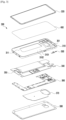
- FIG. 3 is an exploded perspective view of a mobile electronic device shown in FIG. 1 according to an embodiment of the disclosure.
- a mobile electronic device 300 may include a lateral bezel structure 310, a first support member 311 (e.g., a bracket), a front plate 320, a display 400, an electromagnetic induction panel (not shown), a printed circuit board (PCB) 340, a battery 350, a second support member 360 (e.g., a rear case), an antenna 370, and a rear plate 380.
- the mobile electronic device 300 may omit at least one (e.g., the first support member 311 or the second support member 360) of the above components or may further include another component.
- Some components of the electronic device 300 may be the same as or similar to those of the mobile electronic device 100 shown in FIG. 1 or FIG. 2 , thus, descriptions thereof may not be repeated below.
- the first support member 311 is disposed inside the mobile electronic device 300 and may be connected to, or integrated with, the lateral bezel structure 310.
- the first support member 311 may be formed of, for example, a metallic material and/or a non-metal (e.g., polymer) material.
- the first support member 311 may be combined with the display 400 at one side thereof and also combined with the printed circuit board (PCB) 340 at the other side thereof.
- PCB 340 On the PCB 340, a processor, a memory, and/or an interface may be mounted.
- the processor may include, for example, one or more of a central processing unit (CPU), an application processor (AP), a graphics processing unit (GPU), an image signal processor (ISP), a sensor hub processor, or a communications processor (CP).
- CPU central processing unit
- AP application processor
- GPU graphics processing unit
- ISP image signal processor
- sensor hub processor or a communications processor (CP).
- CP communications processor
- the memory may include, for example, one or more of a volatile memory and a nonvolatile memory.
- the interface may include, for example, a high definition multimedia interface (HDMI), a USB interface, a secure digital (SD) card interface, and/or an audio interface.
- HDMI high definition multimedia interface
- USB USB interface
- SD secure digital
- audio audio interface
- the interface may electrically or physically connect the mobile electronic device 300 with an external electronic device and may include a USB connector, an SD card/multimedia card (MMC) connector, or an audio connector.
- MMC multimedia card
- the battery 350 is a device for supplying power to at least one component of the mobile electronic device 300, and may include, for example, a non-rechargeable primary battery, a rechargeable secondary battery, or a fuel cell. At least a part of the battery 350 may be disposed on substantially the same plane as the PCB 340. The battery 350 may be integrally disposed within the mobile electronic device 300, and may be detachably disposed from the mobile electronic device 300.
- the antenna 370 may be disposed between the rear plate 380 and the battery 350.
- the antenna 370 may include, for example, a near field communication (NFC) antenna, a wireless charging antenna, and/or a magnetic secure transmission (MST) antenna.
- NFC near field communication
- MST magnetic secure transmission
- the antenna 370 may perform short-range communication with an external device, or transmit and receive power required for charging wirelessly.
- An antenna structure may be formed by a part or combination of the lateral bezel structure 310 and/or the first support member 311.
- a first support member 311 of a side member (e.g., bezel) 310 may include a first surface 3101 directed towards a front plate 320 and a second surface 3102 directed in an opposite direction (e.g., rear plate direction) to the first surface 3101.
- a camera module 500 e.g., camera module 105 of FIG. 1
- the camera module 500 may be disposed to project or to be seen in a direction of the front plate 320 through a through-hole 301 connected from the first surface 3101 to the second surface 3102 of the first support member 311.
- a portion projecting through the through-hole 301 of the camera module 500 may be disposed to detect an external environment in a location corresponding to a display 400.
- the through-hole 301 may be unnecessary.
- FIG. 4 is an exploded perspective view of a display 400 according to various embodiments of the disclosure.
- the display 400 of FIG. 4 may be at least partly similar to the display 101 of FIG. 1 , or may further include another embodiment of the display.
- the display 400 may include a polarizer (POL) 432 (e.g., polarizing film) disposed on a rear surface of a front cover 320 (e.g., front plate, glass plate, first cover member, or cover member) through an adhesive member (e.g., adhesive member 410 of FIG. 5 ), and at least one subsidiary material layer 440 attached to a rear surface of the display panel 431.
- the adhesive member may include an optical clear adhesive (OCA), a pressure sensitive adhesive (PSA), a thermo-reactive adhesive, a general adhesive, or a double sided tape.
- the display panel 431 and the POL 432 may be integrally formed.
- the display 400 may include a control circuit (not illustrated).
- the control circuit may include a flexible printed circuit board (FPCB) electrically connecting a main printed circuit board (e.g., printed circuit board 340 of FIG. 3 ) of an electronic device (e.g., electronic device 300 of FIG. 3 ) and the display panel 431 with each other, and a display driver IC (DDI) mounted on the FPCB.
- the display 400 may additionally include a touch panel 433.
- the control circuit may include a touch display driver IC (TDDI).
- the display 400 may include a fingerprint sensor (not illustrated) disposed around the control circuit.
- the fingerprint sensor may include an ultrasonic or optical fingerprint sensor capable of recognizing the fingerprint of a finger contacting or approaching from an outer surface of the front cover 320 through a hole formed at least partly on some constituent elements of the display 400.
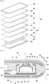
- the at least one subsidiary material layer 440 may include at least one polymer member 441 and 442 disposed on the rear surface of the display panel 431, at least one functional member 443 disposed on a rear surface of the at least one polymer member 441 and 442, and a conductive member 444 disposed on a rear surface of the at least one functional member 443.
- the at least one polymer member 441 and 442 may include a shading layer 441 (e.g., black layer including an uneven pattern) for removing bubbles that may be generated between the display panel 431 and its lower attachments and blocking light created from the display panel 431 or incident from an outside and/or a buffer layer 442 disposed to buffer impacts.
- the at least one functional member 443 may include a heat dissipation sheet (e.g., graphite sheet) for heat dissipation, an added display, a force touch FPCB, a fingerprint sensor FPCB, an antenna radiator for communication, conductive/non-conductive tape, or an open cell sponge.
- the conductive member 444 may include, for example, a metal plate, may be used to provide stiffness reinforcement of the electronic device (e.g., electronic device 300 of FIG. 3 ), to shield surrounding noises, and to disperse heat emitted from surrounding heat emission components.
- the conductive member 444 may include Cu, Al, Mg, SUS, CLAD, or the like (e.g., lamination member on which SUS and Al are alternately disposed).
- the display 400 may further include a detection member 445 to detect an input by an electromagnetic induction type writing member (e.g., electronic pen).
- the detection member 445 may include a digitizer.
- the detection member 445 may be disposed between the at least one polymer member 442 and the functional member 443.
- the detection member 445 may be disposed between the display panel 431 and the at least one polymer member 441.
- the display 400 may be disposed inside the display panel 431, between the display panel 431 and the POL 432, or between the display panel 431 and the subsidiary material layer 440, and may include a light blocking member (e.g., light blocking member 460 of FIG. 6A ) serving as an aperture.
- the light blocking member 460 is disposed closer to the camera module (e.g., camera module 500 of FIG. 5 ) than the existing printing area to minimize and/or reduce the viewing angle, and thus the size of a camera exposure area (e.g., circular BM area), which is seen from the outside of the front cover 320 through the light blocking member 460 serving as the aperture, may be reduced.
- the subsidiary material layer 440 may include openings 4411, 4421, 4451, and 4441 formed in a location corresponding to the camera module (e.g., camera module 500 of FIG. 5 ).
- the camera module 500 may be disposed close to the rear surface of the display panel 431 through the openings 4411, 4421, 4451, and 4441.
- the POL 432 or the touch panel 433 disposed on the upper portion of the display panel 431 may also include openings 4321 and 4331 formed by perforating the corresponding location in order to prevent and/or reduce the performance of the camera module 500 from deteriorating due to the refractive index.
- the POL 432 and/or the touch panel 433 may be processed so that the corresponding location to the camera module 500 becomes transparent or the polarizing characteristic thereof is removed.
- the layers having no opening e.g., display panel 431 or touch panel 433 may include coatings capable of being index-matched to minimize and/or reduce a difference in refractive index between the layers.
- the display 400 includes an organic light-emitting diode (OLED) display, and in examples not forming part of the claimed invention, a liquid crystal display (LCD), or the like.
- FIG. 5 is a partial cross-sectional view of an electronic device, taken along line A-A' of FIG. 1 according to various embodiments of the disclosure.
- an unbreakable (UB) type OLED display e.g., curved display
- the display in examples not forming part of the claimed invention, is not limited thereto.
- AOLED organic light-emitting diode
- OCTA on-cell touch active matrix organic light-emitting diode
- an electronic device 300 may include a front cover 320 (e.g., cover member, front plate, front window, or first plate) directed in a first direction (1 direction), a rear cover 380 (e.g., rear cover member, rear plate, rear window, or second plate) directed in an opposite direction to the front cover 320, and a side member (e.g., bezel) 310 surrounding a space 3001 between the front cover 320 and the rear cover 380.
- the electronic device 300 may include a first waterproof member 3201 disposed between the subsidiary material layer 440 of the display 400 and the side member 310.
- the electronic device 300 may include a second waterproof member 3801 disposed between the side member 310 and the rear plate 380.
- the first waterproof member 3201 and the second waterproof member 3801 may prevent and/or reduce external foreign substances or moisture from flowing into the internal space 3001 of the electronic device 300.
- the waterproof member may be disposed on at least a part of a mount support structure between the camera module 500 and the side member 310.
- the first waterproof member 3201 and/or the second waterproof member 3801 may be replaced by cohesive members.
- the side member 310 may further include a first support member 311 at least partly extending in the internal space 3001 of the electronic device 300.
- the first support member 311 may be formed by a structural coupling to the side member 310.
- the first support member 311 may support the camera module 500 so that the camera module 500 is aligned and disposed around the rear surface of the display panel 431 through the opening (e.g., opening (OP) of FIG. 6A ) of the subsidiary material layer 440 of the display 400.
- the camera module 500 includes a camera housing 510, a lens housing 520 disposed in an internal space 5101 of the camera housing 510 and projecting at least partly in a display direction (e.g., 1 direction), a plurality of lenses 530: 531, 532, 533, and 534 disposed at predetermined intervals in an internal space 5201 of the lens housing 520, and at least one image sensor 540 disposed to acquire at least a part of light having passed through the plurality of lenses 530: 531, 532, 533, and 534 in the internal space 5101 of the camera housing 510.
- a display direction e.g., 1 direction
- a plurality of lenses 530: 531, 532, 533, and 534 disposed at predetermined intervals in an internal space 5201 of the lens housing 520
- at least one image sensor 540 disposed to acquire at least a part of light having passed through the plurality of lenses 530: 531, 532, 533, and 534 in the internal space 5101 of
- the lens housing 520 may move to vary the distance from the display panel 431 through a specific driving unit in the camera housing 510.
- a separate driving unit may be disposed to change the location of at least one of the plurality of lenses 530.
- the camera housing 510 may be omitted, and the lens housing 520 may be directly disposed on the first support member 311 through a specific alignment process.
- the camera housing 510 may be omitted to reduce the camera disposition space, and the lens housing 520 may be disposed to be attached to one side surface of the first support member 311.
- the camera module 500 may be aligned through a through-hole 301 of the first support member 311, and may be attached to the rear surface of the first support member 311 through an adhesive member 312 (e.g., bonding member or tape member).
- the display 400 may include the touch panel (e.g., touch panel 433 of FIG. 4 ), the POL 432, the display panel 431, the shading layer 441, the buffer layer (e.g., buffer layer 442 of FIG. 4 ), the digitizer (e.g., digitizer 445 of FIG. 4 ), the functional member (e.g., functional member 443 of FIG. 4 ), and/or the conductive member (e.g., conductive member 444 of FIG. 4 ).
- the camera module 500 may be supported by a second support member 360 (e.g., rear case) additionally disposed in the internal space of the electronic device.
- FIG. 6A is an enlarged view of an area B of FIG. 5 according to various embodiments of the disclosure.
- FIG. 6B is a partial plan view of an electronic device 300 as seen from above a front cover 320 according to various embodiments of the disclosure.
- the electronic device 300 may include the adhesive layer 410 disposed between the rear surface of the front cover 320 and the side member 310, the POL 432, the display panel 431, and the subsidiary material layer 440.
- the POL 432 may include the opening 4321 formed to improve optical permeability of the camera module 500.
- a part of the adhesive member 410 disposed on the upper portion of the POL 432, which corresponds to the opening 4321 may also be omitted at least partly.
- the opening 4321 formed on the POL 432 may be filled with a material to match the refraction index in accordance with an increase of interfacial reflection.
- the area of the POL 432 corresponding to the plurality of lenses 530 may not include the opening 4321 formed thereon, and may be formed with high permeability.
- at least a partial area (e.g., area corresponding to the plurality of lenses 530) of the POL 432 may be formed of a material having permeability different from the permeability of the other area of the POL 432, or may include another member capable of heightening the permeability.
- a member (not illustrated) for heightening the permeability may be disposed on at least a part (e.g., upper side surface or lower side surface) of the area corresponding to the plurality of lenses 530 of the POL 432.
- the subsidiary material layer 440 may include an opening OP formed on an area at least partly overlapping the plurality of lenses 530.
- the opening OP may be formed as one opening OP on the subsidiary material layer 440 by making the opening (e.g., opening 4411 of FIG. 4 ) formed on the shading layer 441, the opening (e.g., opening 4421 of FIG. 4 ) formed on the buffer layer 442, the opening (e.g., opening 4431 of FIG. 4 ) formed on the functional member 443, and the opening (e.g., opening 4441 of FIG. 4 ) formed on the conductive member 444 overlap one another.
- the respective openings may have different sizes corresponding to the shape of the camera module.
- the display 400 includes at least one light blocking member (e.g., including a light blocking material) 460 disposed in the display panel 431.
- the light blocking member 460 e.g., aperture
- the light blocking member 460 includes a light transmission region(e.g., a light transmission aperture) AD corresponding to an area overlapping an effective diameter of the lens 530.
- the overall outer diameter OD of the light blocking member 460 may be formed corresponding to the light transmission region AD and a blocking area DS (e.g., aperture area) forming the light transmission region AD.
- the area of the light blocking member 460 may be formed as a sum of the light transmission region AD and the blocking area DS forming the light transmission region AD.
- the outer diameter OD crossing the light blocking member 460 may be formed by the sum of the length AD crossing the light transmission region AD and the length DS crossing the blocking area.
- the size of the light transmission region AD or the blocking area DS may be determined by the size, disposition, and location of the lens 530.
- the size of the light transmission region AD of the light blocking member 460 may be determined based on a predetermined viewing angle of the lens 530 of the camera module 500.
- the blocking area DS of the light blocking member 460 may be determined to have a size enough to block the unnecessary light so that at least a part of the light flowing from outside or inside does not flow into the neighborhood of the light transmission region AD of the display panel 431.
- the light transmission region AD may be formed as an opening, and the opening may be formed by the blocking area DS. Through the formed opening, at least a part of external light outside the electronic device may flow in and may be transferred to the image sensor 540 through the lens 530. The amount of light flowing into the image sensor may be determined by the aperture, and as the size of the light transmission region AD is increased, a larger amount of light may flow into the image sensor.
- the display panel 431 may be configured so that pixels and/or wirings are not disposed on the area overlapping the light transmission region AD to improve the optical permeability as seen from above the front cover 320.
- the display panel 431 may be configured so that the area overlapping the light transmission region (AD) has a lower pixel density and/or a lower wiring density than the pixel density and/or the wiring density of a neighboring active area (e.g., active area) to improve the optical permeability.
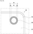
- FIG. 7 is a partial cross-sectional view of a display panel 431 with an area C of FIG. 6A enlarged according to various embodiments of the disclosure.
- the display panel 431 includes a substrate layer 431a, an intermediate layer 431b laminated on the substrate layer 431a, and an encapsulation (encap) layer 431c laminated on the intermediate layer 431b.
- the display panel 431 includes a plurality of pixels, each of which may include a first sub-pixel area (pixel red (Pr)), a second sub-pixel area (pixel green (Pg)), and a third sub-pixel area (pixel blue (Pb)).
- the area in which the plurality of pixels are disposed may include the active area of the display panel 431.
- the display panel 431 may include a first pixel electrode 4311a, a second pixel electrode 4311b, and a third pixel electrode 4311c being disposed on the substrate layer 431a to correspond to the first sub-pixel area (Pr), the second sub-pixel area (Pg), and the third sub-pixel area (Pb) in the intermediate layer 431b.
- the display panel 431 may include a first organic material layer 4312a, a second organic material layer 4312b, and a third organic material layer 4312c respectively disposed on upper portions of the first to third pixel electrodes 4311a, 4311b, and 4311c, respectively, in the intermediate layer 431b.
- the first to third sub-pixel areas may be partitioned by a pixel defining layer 4314 of, for example, an insulation material, and an opposite electrode 4313 is commonly disposed on the first to third organic material layers 4312a, 4312b, and 4312c.
- the first to third pixel electrodes 4311a, 4311b, and 4311c may be reflective electrodes including reflective layers.
- the reflective layer may include, for example, and without limitation, at least any one selected from the group including silver (Ag), magnesium (Mg), aluminum (Al), platinum (Pt), palladium (Pd), gold (Au), nickel (Ni), neodymium (Nd), iridium (Ir), chrome (Cr), or the like, and on the reflective layer, a transparent or semi-transparent electrode layer formed, for example, and without limitation, by at least any one selected from the group including indium tin oxide (ITO), indium zinc oxide (IZO), zinc oxide (ZnO), indium oxide (In2O3), indium gallium oxide (IGO), aluminum zinc oxide (AZO), or the like, may be further disposed.
- a transparent or semi-transparent electrode layer formed, for example, and without limitation, by at least any one selected from the group including indium tin oxide (ITO), indium zinc oxide (IZO), zinc oxide (ZnO), indium oxide (In2O3), indium gallium oxide (IGO
- each of the first to third organic material layers 4312a, 4312b, and 4312c may include an organic light-emitting layer emitting light of a first color, a second color, and a third color.
- the organic light-emitting layer may be disposed between a pair of common layers vertically laminated.
- one common layer may include a hole injection layer (HIL) and/or a hole transport layer (HTL).
- the other common layer may include an electron transport layer (ETL) and/ or an electron injection layer (EIL).
- the common layers are not limited thereto, but may further include various functional layers while including the organic light-emitting layer.
- the above-described first to third colors may be red, green, and blue, respectively.
- the first to third colors are not limited thereto, but other various color combinations may be used in addition to combinations of red, green, and blue if they can emit a white light.
- the opposite electrode 4313 may include a transparent or semi-transparent electrode, and may include, for example, and without limitation, one or more materials selected from silver (Ag), aluminum (Al), magnesium (Mg), lithium (Li), calcium (Ca), copper (Cu), LiF/Ca, LiF/Al, MgAg, CaAg, or the like, and may be formed of a thin film having a thickness of several to several tens of nanometers (nm).
- the light emitted from the first to third organic light-emitting layers included in the first to third organic material layers 4312a, 4312b, and 4312c may be emitted in the direction of the opposite electrode 4313 directly or after being reflected by the first to third pixel electrodes 4311a, 4311b, and 4311c.
- the substrate layer 431a may include electrical connection members electrically connected to the first to third pixel electrodes 4311a, 4311b, and 4311c, respectively.
- the electrical connection member may include, for example, and without limitation, a thin film transistor (TFT), a low-temperature passivation transistor (LTPS), or the like.
- the encap layer 431c may be disposed on the upper portion of the opposite electrode 4313 for the protection thereof.
- the display panel 431 includes the light blocking member 460 disposed in the intermediate layer 431b between the substrate layer 431a and the encap layer 431c in the blocking area (e.g., blocking area DS of FIG. 6A ).
- the first to third pixel electrodes 4311a, 4311b, and 4311c, the first to third organic material layers 4312a, 4312b, and 4312c, or the opposite electrode 4313 may not be disposed in the intermediate layer 431b.
- the intermediate layer 431b may include only a fourth pixel electrode 4311d that is substantially the same as the first to third pixel electrodes 4311a, 4311b, and 4311c.
- the light blocking member 460 may include an organic material or sealant of an opaque (black) material formed together when the first to third organic material layers 4312a, 4312b, and 4312c are formed.
- the light blocking member 460 may be replaced by the first to third pixel electrodes 4311a, 4311b, and 4311c disposed on the upper portion of the substrate 431a with a high disposition density on the intermediate layer 431b.
- the light blocking member 460 may be separately disposed or printed using an opaque material (ink or resin).
- the light blocking member 460 may be formed using the existing opaque constituent element (electrode or wiring) inside the display.
- FIGS. 8 and 9 are partial cross-sectional views of an electronic device including light blocking members 461 and 462 disposed on a display according to various embodiments of the disclosure, not forming part of the claimed invention.
- the light blocking member 461 may be disposed between the display panel 431 and the POL 432. According to an embodiment, the light blocking member 461 may be disposed on the upper surface of the display panel 431 or the rear surface of the POL 432.
- the light blocking member 462 may be disposed between the display panel 431 and the subsidiary material layer 440. According to an embodiment, the light blocking member 462 may be disposed on the rear surface of the display panel 431 or the upper surface of the subsidiary material layer 444.
- the size of the light transmission region of the light blocking member 461 and 462 may be determined in accordance with the separation distance from the camera module 500 and/or the predetermined viewing angle of the camera module 500.
- the light blocking member 461 and 462 may include a light blocking material, such as, for example, and without limitation, a black printed layer, a black matrix (BM), an opaque tape member, or the like.
- the light blocking member 461 and 462 may be disposed to at least partly overlap the opening 4321 as seen from above the electronic device 300.
- the light blocking member 461 and 462 may be disposed between various layers.
- the light blocking member may be disposed between the adhesive member 410 and the POL 432.
- the light blocking member 461 and 462 may be disposed to at least partly overlap each other in at least two areas between the display panel 431 and the POL 432, between the display panel 431 and the subsidiary material layer 440, inside the display panel 431, or between the adhesive member 410 and the POL 432.
- FIG. 10 is a partial cross-sectional view of an electronic device 300 according to various embodiments of the disclosure, not forming part of the claimed invention.
- the light blocking member may be disposed or shaped so that a separate member is not added, and at least one of elements 441, 442, 443, and 444 of the subsidiary material layer 440 disposed on the rear surface of the display panel 431 may serve as the light blocking member.
- the subsidiary material layer 440 at least a part of the shading layer 441 of the opaque material facing the display panel 431 may be used as the light blocking member.
- the openings e.g., openings 4421, 4431, and 4441 of FIG.
- the opening 4411 of the shading layer 441 may be formed in the shape of the light transmission region (e.g., light transmission region AD of FIG. 6A ) corresponding to the camera module 500.
- the light blocking member may be formed through at least two layers of the subsidiary material layers 440.
- an electronic device e.g., electronic device 300 of FIG. 5
- a lens housing e.g., lens housing 520 of FIG.
- the display includes: a display panel (e.g., display panel 431 of FIG. 5 ) and a light blocking member (light blocking member 460 of FIG. 6A ) comprising a light blocking material, the light blocking member including a light transmission region (e.g., light transmission region AD of FIG. 6A ) and being disposed inside of the display panel, the light transmission region overlapping at least parts of the plurality of lenses as viewed from above the display.
- a display panel e.g., display panel 431 of FIG. 5
- a light blocking member comprising a light blocking material
- the light blocking member including a light transmission region (e.g., light transmission region AD of FIG. 6A ) and being disposed inside of the display panel, the light transmission region overlapping at least parts of the plurality of lenses as viewed from above the display.
- the display panel includes a substrate layer; an intermediate layer including a plurality of pixel electrodes laminated on an upper portion of the substrate layer, organic light-emitting layers disposed on the plurality of pixel electrodes, respectively, and an opposite electrode disposed on upper portions of the organic light-emitting layers; and an encapsulation layer disposed on an upper portion of the intermediate layer, wherein the light blocking member is disposed in the intermediate layer.
- the light blocking member may include an organic material having reflectivity of about 99% or more with respect to light flowing into the light blocking member.
- the size of the light transmission region of the light blocking member may be determined based on a viewing angle of the camera module.
- an area overlapping the light transmission region of the display panel may not include the organic light-emitting layers as viewed from above the display.
- the electrodes may not be disposed in an area overlapping the light transmission region of the display panel as viewed from above the display.
- a disposition density of the plurality of electrodes and/or the organic light-emitting layers may be configured to be lower than a disposition density of the neighboring display area in an area overlapping the light transmission region of the display panel as viewed from above the display.
- the display may include a polarizing member (POL) including a polarizer laminated on an upper portion of the display panel.
- POL polarizing member
- the polarizing member may include an opening corresponding to the light transmission region as viewed from above the display.
- the display may include at least one subsidiary material layer laminated on a lower portion of the display panel.
- the at least one subsidiary material layer may include an opening corresponding to the light transmission region as viewed from above the display.
- the camera module may be at least partially disposed in the opening.
- the at least one subsidiary material layer may include at least one polymer layer disposed on a rear surface of the display panel, a functional member comprising a heat dissipating material layer disposed under the at least one polymer layer, and a conductive plate disposed under the functional member layer.
- the light transmission region may be formed through the opening having the same center as centers of the plurality of lenses on the at least one polymer layer.
- the at least one polymer layer may include a shading layer of an opaque material.
Landscapes
- Engineering & Computer Science (AREA)
- Signal Processing (AREA)
- Physics & Mathematics (AREA)
- Optics & Photonics (AREA)
- Microelectronics & Electronic Packaging (AREA)
- Multimedia (AREA)
- General Physics & Mathematics (AREA)
- Computer Networks & Wireless Communication (AREA)
- Geometry (AREA)
- Devices For Indicating Variable Information By Combining Individual Elements (AREA)
- Chemical & Material Sciences (AREA)
- Inorganic Chemistry (AREA)
- Life Sciences & Earth Sciences (AREA)
- Sustainable Development (AREA)
Claims (10)
- Elektronische Vorrichtung (100, 300), umfassend:ein Gehäuse (110, 310);eine Anzeige (101, 400), die in einem Innenraum (3001) des Gehäuses so angeordnet ist, dass sie von einer Außenseite aus betrachtbar ist, und einen Anzeigebereich beinhaltet; undein Kameramodul (105, 500), das unter der Anzeige angeordnet ist, dabei mindestens einen Teil des Anzeigebereichs überlappt und keine Blendenstruktur beinhaltet,wobei das Kameramodul beinhaltet:ein Objektivgehäuse (520);eine Vielzahl von Objektiven (530), die auf dem Objektivgehäuse angeordnet sind; undeinen Bildsensor (540), der unter der Vielzahl von Objektiven angeordnet ist,wobei die Anzeige beinhaltet:eine Anzeigetafel (431), undein Lichtblockierungselement (460, 461, 462), das im Inneren der Anzeigetafel angeordnet ist, wobei das Lichtblockierungselement eine Lichtdurchgangsregion (AD) beinhaltet, die Lichtdurchgangsregion mindestens Teile der Vielzahl von Objektiven überlappt, wie von oberhalb der Anzeige betrachtet, wobei die Anzeigetafel umfasst:eine Substratschicht (431a);eine Zwischenschicht (431b) einschließlich einer Vielzahl von Pixelelektroden (4311a, 4311b, 4311c), die auf einem oberen Abschnitt der Substratschicht laminiert sind, organischer lichtemittierender Schichten (4312a, 4312b, 4312c), die jeweils auf der Vielzahl von Pixelelektroden angeordnet sind, und einer gegenüberliegenden Elektrode (4313), die auf oberen Abschnitten der organischen lichtemittierenden Schichten angeordnet ist; undeine Verkapselungsschicht (431c), die auf einem oberen Abschnitt der Zwischenschicht angeordnet ist, undwobei das Lichtblockierungselement in der Zwischenschicht direkt zwischen der Substratschicht und der Verkapselungsschicht angeordnet ist und an die organischen lichtemittierenden Schichten und die gegenüberliegende Elektrode der Zwischenschicht in einer Richtung parallel zu dem oberen Abschnitt der Substratschicht angrenzt.
- Elektronische Vorrichtung (100, 300) nach Anspruch 1, wobei das Lichtblockierungselement (460, 461, 462) ein organisches Material mit einer Reflektivität von etwa 99 % oder mehr in Bezug auf in das Lichtblockierungselement einströmendes Licht umfasst.
- Elektronische Vorrichtung (100, 300) nach Anspruch 1, wobei eine Größe der Lichtdurchgangsregion (AD) des Lichtblockierungselements (460, 461, 462) basierend auf einem Betrachtungswinkel des Kameramoduls (105, 500) bestimmt wird.
- Elektronische Vorrichtung (100, 300) nach Anspruch 1, wobei ein Bereich, der die Lichtdurchgangsregion (AD) der Anzeigetafel (431) überlappt, nicht die organischen lichtemittierenden Schichten (4312a, 4312b, 4312c) beinhaltet, wie von oberhalb der Anzeige (101, 400) betrachtet.
- Elektronische Vorrichtung (100, 300) nach Anspruch 1, wobei die Elektroden (4311a, 4311b, 4311c) nicht in einem Bereich angeordnet sind, der die Lichtdurchgangsregion (AD) der Anzeigetafel (431) überlappt, wie von oberhalb der Anzeige (101, 400) betrachtet.
- Elektronische Vorrichtung (100, 300) nach Anspruch 1, wobei eine Dispositionsdichte der Vielzahl von Elektroden (4311a, 4311b, 4311c) und/oder der organischen lichtemittierenden Schichten (4312a, 4312b, 4312c) weniger ist als eine Dispositionsdichte eines benachbarten Anzeigebereichs in einem Bereich, der die Lichtdurchgangsregion (AD) der Anzeigetafel (431) überlappt, wie von oberhalb der Anzeige (101, 400) betrachtet.
- Elektronische Vorrichtung (100, 300) nach Anspruch 1, wobei die Anzeige (101, 400) ein Polarisationselement (432) umfasst, das einen Polarisator umfasst, der auf einem oberen Abschnitt der Anzeigetafel (431) laminiert ist.
- Elektronische Vorrichtung (100, 300) nach Anspruch 7, wobei das Polarisationselement (432) eine Öffnung (4321) beinhaltet, die der Lichtdurchgangsregion (AD) entspricht, wie von oberhalb der Anzeige (101, 400) betrachtet.
- Elektronische Vorrichtung (100, 300) nach Anspruch 1, wobei die Anzeige (101, 400) mindestens eine zusätzliche Materialschicht (440) umfasst, die auf einem unteren Abschnitt der Anzeigetafel (431) laminiert ist.
- Elektronische Vorrichtung (100, 300) nach Anspruch 9, wobei die mindestens eine zusätzliche Materialschicht (440) eine Öffnung (4411) beinhaltet, die der Lichtdurchgangsregion (AD) entspricht, wie von oberhalb der Anzeige (101, 400) betrachtet.
Applications Claiming Priority (2)
| Application Number | Priority Date | Filing Date | Title |
|---|---|---|---|
| KR1020190110637A KR102713286B1 (ko) | 2019-09-06 | 2019-09-06 | 카메라 모듈을 포함하는 전자 장치 |
| PCT/KR2020/012039 WO2021045593A1 (en) | 2019-09-06 | 2020-09-07 | Electronic device including camera module |
Publications (3)
| Publication Number | Publication Date |
|---|---|
| EP3987758A1 EP3987758A1 (de) | 2022-04-27 |
| EP3987758A4 EP3987758A4 (de) | 2022-08-24 |
| EP3987758B1 true EP3987758B1 (de) | 2025-03-05 |
Family
ID=74851421
Family Applications (1)
| Application Number | Title | Priority Date | Filing Date |
|---|---|---|---|
| EP20860351.4A Active EP3987758B1 (de) | 2019-09-06 | 2020-09-07 | Elektronische vorrichtung mit kameramodul |
Country Status (4)
| Country | Link |
|---|---|
| US (1) | US11930686B2 (de) |
| EP (1) | EP3987758B1 (de) |
| KR (1) | KR102713286B1 (de) |
| WO (1) | WO2021045593A1 (de) |
Families Citing this family (9)
| Publication number | Priority date | Publication date | Assignee | Title |
|---|---|---|---|---|
| CN110784635B (zh) * | 2019-11-18 | 2021-05-18 | 维沃移动通信有限公司 | 电子设备 |
| JP2024521239A (ja) | 2021-04-05 | 2024-05-29 | サムスン エレクトロニクス カンパニー リミテッド | カメラモジュールを含む電子装置 |
| KR102850002B1 (ko) * | 2021-04-19 | 2025-08-26 | 삼성전자주식회사 | 난반사 구조의 디스플레이를 포함하는 전자 장치 |
| TWI809386B (zh) * | 2021-05-06 | 2023-07-21 | 金佶科技股份有限公司 | 取像裝置 |
| CN113327519A (zh) * | 2021-06-23 | 2021-08-31 | 京东方科技集团股份有限公司 | 显示模组及显示装置 |
| CN215835423U (zh) * | 2021-08-18 | 2022-02-15 | 荣耀终端有限公司 | 电子设备 |
| US12192613B2 (en) * | 2022-05-19 | 2025-01-07 | Dell Products L.P. | Advanced indicator system with colorful e-ink layer for embedded camera display |
| KR20240018818A (ko) * | 2022-08-03 | 2024-02-14 | 엘지디스플레이 주식회사 | 표시 장치 |
| US20240103352A1 (en) * | 2022-09-23 | 2024-03-28 | Apple Inc. | Co-Design of a Camera Module and a Display |
Family Cites Families (16)
| Publication number | Priority date | Publication date | Assignee | Title |
|---|---|---|---|---|
| US6414337B1 (en) | 2000-11-10 | 2002-07-02 | Three-Five Systems, Inc. | Aperture frame for liquid crystal display device |
| KR102031654B1 (ko) * | 2012-05-23 | 2019-10-15 | 삼성디스플레이 주식회사 | 윈도우 구조물, 그 제조 방법, 윈도우 구조물을 포함하는 카메라가 탑재된 전자 장치 및 그 제조 방법 |
| KR102524754B1 (ko) * | 2015-09-09 | 2023-04-21 | 엘지디스플레이 주식회사 | 표시 장치 |
| KR102501111B1 (ko) | 2015-12-28 | 2023-02-16 | 엘지디스플레이 주식회사 | 카메라 모듈 일체형 액정 표시 장치 및 그 제조 방법 |
| KR20170111827A (ko) * | 2016-03-29 | 2017-10-12 | 삼성전자주식회사 | 디스플레이 및 카메라를 포함하는 전자 장치 |
| JP6807223B2 (ja) | 2016-11-28 | 2021-01-06 | 株式会社ジャパンディスプレイ | 表示装置 |
| CN107241466B (zh) * | 2017-05-04 | 2020-01-31 | Oppo广东移动通信有限公司 | 显示装置及移动终端 |
| WO2018216545A1 (ja) * | 2017-05-22 | 2018-11-29 | シャープ株式会社 | 表示デバイス |
| KR20190000522A (ko) * | 2017-06-23 | 2019-01-03 | 삼성전자주식회사 | 복수의 전극을 연결하는 도전성 배선 및 노이즈 신호를 차폐하기 위한 도전 영역을 포함하는 도전층이 형성된 터치 패널 및 그것을 포함하는 전자 장치 |
| KR102372809B1 (ko) * | 2017-07-04 | 2022-03-15 | 삼성전자주식회사 | 틸팅 구조를 갖는 이미징 센서 어셈블리 및 그것을 포함하는 전자 장치 |
| CN109427853B (zh) * | 2017-09-05 | 2023-05-30 | 乐金显示有限公司 | 包括指纹扫描器的显示装置 |
| US10620665B2 (en) * | 2018-02-05 | 2020-04-14 | Guangdong Oppo Mobile Telecommunications Corp., Lt | Terminal display assembly and mobile terminal |
| CN110112200A (zh) * | 2019-05-21 | 2019-08-09 | 武汉天马微电子有限公司 | 显示面板和显示装置 |
| CN110062082B (zh) | 2019-05-24 | 2024-05-17 | Oppo广东移动通信有限公司 | 一种显示屏及终端设备 |
| CN110149470B (zh) * | 2019-06-28 | 2024-05-31 | Oppo广东移动通信有限公司 | 电子设备 |
| KR102664694B1 (ko) * | 2019-08-16 | 2024-05-09 | 삼성전자 주식회사 | 카메라 모듈을 포함하는 전자 장치 |
-
2019
- 2019-09-06 KR KR1020190110637A patent/KR102713286B1/ko active Active
-
2020
- 2020-09-07 EP EP20860351.4A patent/EP3987758B1/de active Active
- 2020-09-07 WO PCT/KR2020/012039 patent/WO2021045593A1/en not_active Ceased
- 2020-09-08 US US17/014,325 patent/US11930686B2/en active Active
Also Published As
| Publication number | Publication date |
|---|---|
| US11930686B2 (en) | 2024-03-12 |
| US20210074780A1 (en) | 2021-03-11 |
| EP3987758A1 (de) | 2022-04-27 |
| EP3987758A4 (de) | 2022-08-24 |
| KR20210029431A (ko) | 2021-03-16 |
| WO2021045593A1 (en) | 2021-03-11 |
| KR102713286B1 (ko) | 2024-10-04 |
Similar Documents
| Publication | Publication Date | Title |
|---|---|---|
| EP3987758B1 (de) | Elektronische vorrichtung mit kameramodul | |
| CN111800559B (zh) | 电子装置 | |
| EP4005192B1 (de) | Elektronische vorrichtung mit anzeige und kameravorrichtung | |
| US11503749B2 (en) | Display including shielding member arranged to cover at least part of display driving circuit, and electronic device including same | |
| US11552133B2 (en) | Electronic device including display and camera | |
| ES2743037T3 (es) | Pantalla de visualización, montaje de la pantalla de visualización y terminal | |
| US11178320B2 (en) | Electronic device including electronic component disposed through display | |
| EP3996359B1 (de) | Elektronische vorrichtung mit kameramodul | |
| US12141409B2 (en) | Electronic device including digitizer | |
| US12169423B2 (en) | Flexible display module including shielding structure and waterproof structure and electronic device including the same | |
| US20190377925A1 (en) | Display device with integrated sensor opening | |
| US10855823B2 (en) | Terminal | |
| US20230050153A1 (en) | Electronic device including under display camera and display included in the same | |
| KR20230149626A (ko) | Udc를 포함한 전자 장치 | |
| EP4290577A1 (de) | Elektronische vorrichtung mit anzeige | |
| EP4369891B1 (de) | Elektronische vorrichtung mit udc | |
| US20230345779A1 (en) | Electronic device including under display camera | |
| KR20240029681A (ko) | 표시 장치 | |
| CN117694034A (zh) | 包括显示器下相机的电子装置和电子装置中包括的显示器 | |
| KR20210017101A (ko) | 디스플레이를 포함하는 전자 장치 |
Legal Events
| Date | Code | Title | Description |
|---|---|---|---|
| STAA | Information on the status of an ep patent application or granted ep patent |
Free format text: STATUS: THE INTERNATIONAL PUBLICATION HAS BEEN MADE |
|
| PUAI | Public reference made under article 153(3) epc to a published international application that has entered the european phase |
Free format text: ORIGINAL CODE: 0009012 |
|
| STAA | Information on the status of an ep patent application or granted ep patent |
Free format text: STATUS: REQUEST FOR EXAMINATION WAS MADE |
|
| 17P | Request for examination filed |
Effective date: 20220118 |
|
| AK | Designated contracting states |
Kind code of ref document: A1 Designated state(s): AL AT BE BG CH CY CZ DE DK EE ES FI FR GB GR HR HU IE IS IT LI LT LU LV MC MK MT NL NO PL PT RO RS SE SI SK SM TR |
|
| A4 | Supplementary search report drawn up and despatched |
Effective date: 20220721 |
|
| RIC1 | Information provided on ipc code assigned before grant |
Ipc: H01L 27/32 20060101ALI20220715BHEP Ipc: H01L 51/52 20060101ALI20220715BHEP Ipc: H04N 5/225 20060101ALI20220715BHEP Ipc: H04M 1/02 20060101AFI20220715BHEP |
|
| DAV | Request for validation of the european patent (deleted) | ||
| DAX | Request for extension of the european patent (deleted) | ||
| REG | Reference to a national code |
Ref country code: DE Ref legal event code: R079 Free format text: PREVIOUS MAIN CLASS: H04M0001020000 Ipc: H10K0059650000 Ref country code: DE Ref legal event code: R079 Ref document number: 602020047383 Country of ref document: DE Free format text: PREVIOUS MAIN CLASS: H04M0001020000 Ipc: H10K0059650000 |
|
| GRAP | Despatch of communication of intention to grant a patent |
Free format text: ORIGINAL CODE: EPIDOSNIGR1 |
|
| STAA | Information on the status of an ep patent application or granted ep patent |
Free format text: STATUS: GRANT OF PATENT IS INTENDED |
|
| RIC1 | Information provided on ipc code assigned before grant |
Ipc: H10K 50/844 20230101ALI20240917BHEP Ipc: H10K 50/86 20230101ALI20240917BHEP Ipc: H10K 59/12 20230101ALI20240917BHEP Ipc: H10K 59/80 20230101ALI20240917BHEP Ipc: H10K 59/65 20230101AFI20240917BHEP |
|
| INTG | Intention to grant announced |
Effective date: 20241014 |
|
| GRAS | Grant fee paid |
Free format text: ORIGINAL CODE: EPIDOSNIGR3 |
|
| GRAA | (expected) grant |
Free format text: ORIGINAL CODE: 0009210 |
|
| STAA | Information on the status of an ep patent application or granted ep patent |
Free format text: STATUS: THE PATENT HAS BEEN GRANTED |
|
| AK | Designated contracting states |
Kind code of ref document: B1 Designated state(s): AL AT BE BG CH CY CZ DE DK EE ES FI FR GB GR HR HU IE IS IT LI LT LU LV MC MK MT NL NO PL PT RO RS SE SI SK SM TR |
|
| REG | Reference to a national code |
Ref country code: GB Ref legal event code: FG4D |
|
| REG | Reference to a national code |
Ref country code: CH Ref legal event code: EP |
|
| REG | Reference to a national code |
Ref country code: DE Ref legal event code: R096 Ref document number: 602020047383 Country of ref document: DE |
|
| REG | Reference to a national code |
Ref country code: IE Ref legal event code: FG4D |
|
| PG25 | Lapsed in a contracting state [announced via postgrant information from national office to epo] |
Ref country code: RS Free format text: LAPSE BECAUSE OF FAILURE TO SUBMIT A TRANSLATION OF THE DESCRIPTION OR TO PAY THE FEE WITHIN THE PRESCRIBED TIME-LIMIT Effective date: 20250605 |
|
| PG25 | Lapsed in a contracting state [announced via postgrant information from national office to epo] |
Ref country code: FI Free format text: LAPSE BECAUSE OF FAILURE TO SUBMIT A TRANSLATION OF THE DESCRIPTION OR TO PAY THE FEE WITHIN THE PRESCRIBED TIME-LIMIT Effective date: 20250305 |
|
| REG | Reference to a national code |
Ref country code: NL Ref legal event code: MP Effective date: 20250305 |
|
| PG25 | Lapsed in a contracting state [announced via postgrant information from national office to epo] |
Ref country code: ES Free format text: LAPSE BECAUSE OF FAILURE TO SUBMIT A TRANSLATION OF THE DESCRIPTION OR TO PAY THE FEE WITHIN THE PRESCRIBED TIME-LIMIT Effective date: 20250305 |
|
| REG | Reference to a national code |
Ref country code: LT Ref legal event code: MG9D |
|
| PG25 | Lapsed in a contracting state [announced via postgrant information from national office to epo] |
Ref country code: NO Free format text: LAPSE BECAUSE OF FAILURE TO SUBMIT A TRANSLATION OF THE DESCRIPTION OR TO PAY THE FEE WITHIN THE PRESCRIBED TIME-LIMIT Effective date: 20250605 |
|
| PG25 | Lapsed in a contracting state [announced via postgrant information from national office to epo] |
Ref country code: HR Free format text: LAPSE BECAUSE OF FAILURE TO SUBMIT A TRANSLATION OF THE DESCRIPTION OR TO PAY THE FEE WITHIN THE PRESCRIBED TIME-LIMIT Effective date: 20250305 |
|
| PG25 | Lapsed in a contracting state [announced via postgrant information from national office to epo] |
Ref country code: LV Free format text: LAPSE BECAUSE OF FAILURE TO SUBMIT A TRANSLATION OF THE DESCRIPTION OR TO PAY THE FEE WITHIN THE PRESCRIBED TIME-LIMIT Effective date: 20250305 |
|
| PG25 | Lapsed in a contracting state [announced via postgrant information from national office to epo] |
Ref country code: GR Free format text: LAPSE BECAUSE OF FAILURE TO SUBMIT A TRANSLATION OF THE DESCRIPTION OR TO PAY THE FEE WITHIN THE PRESCRIBED TIME-LIMIT Effective date: 20250606 Ref country code: BG Free format text: LAPSE BECAUSE OF FAILURE TO SUBMIT A TRANSLATION OF THE DESCRIPTION OR TO PAY THE FEE WITHIN THE PRESCRIBED TIME-LIMIT Effective date: 20250305 |
|
| REG | Reference to a national code |
Ref country code: AT Ref legal event code: MK05 Ref document number: 1774188 Country of ref document: AT Kind code of ref document: T Effective date: 20250305 |
|
| PG25 | Lapsed in a contracting state [announced via postgrant information from national office to epo] |
Ref country code: NL Free format text: LAPSE BECAUSE OF FAILURE TO SUBMIT A TRANSLATION OF THE DESCRIPTION OR TO PAY THE FEE WITHIN THE PRESCRIBED TIME-LIMIT Effective date: 20250305 |
|
| PG25 | Lapsed in a contracting state [announced via postgrant information from national office to epo] |
Ref country code: SE Free format text: LAPSE BECAUSE OF FAILURE TO SUBMIT A TRANSLATION OF THE DESCRIPTION OR TO PAY THE FEE WITHIN THE PRESCRIBED TIME-LIMIT Effective date: 20250305 |
|
| PG25 | Lapsed in a contracting state [announced via postgrant information from national office to epo] |
Ref country code: SM Free format text: LAPSE BECAUSE OF FAILURE TO SUBMIT A TRANSLATION OF THE DESCRIPTION OR TO PAY THE FEE WITHIN THE PRESCRIBED TIME-LIMIT Effective date: 20250305 |
|
| PG25 | Lapsed in a contracting state [announced via postgrant information from national office to epo] |
Ref country code: PT Free format text: LAPSE BECAUSE OF FAILURE TO SUBMIT A TRANSLATION OF THE DESCRIPTION OR TO PAY THE FEE WITHIN THE PRESCRIBED TIME-LIMIT Effective date: 20250707 |
|
| PGFP | Annual fee paid to national office [announced via postgrant information from national office to epo] |
Ref country code: DE Payment date: 20250820 Year of fee payment: 6 |
|
| PG25 | Lapsed in a contracting state [announced via postgrant information from national office to epo] |
Ref country code: PL Free format text: LAPSE BECAUSE OF FAILURE TO SUBMIT A TRANSLATION OF THE DESCRIPTION OR TO PAY THE FEE WITHIN THE PRESCRIBED TIME-LIMIT Effective date: 20250305 Ref country code: IT Free format text: LAPSE BECAUSE OF FAILURE TO SUBMIT A TRANSLATION OF THE DESCRIPTION OR TO PAY THE FEE WITHIN THE PRESCRIBED TIME-LIMIT Effective date: 20250305 |
|
| PG25 | Lapsed in a contracting state [announced via postgrant information from national office to epo] |
Ref country code: AT Free format text: LAPSE BECAUSE OF FAILURE TO SUBMIT A TRANSLATION OF THE DESCRIPTION OR TO PAY THE FEE WITHIN THE PRESCRIBED TIME-LIMIT Effective date: 20250305 |
|
| PG25 | Lapsed in a contracting state [announced via postgrant information from national office to epo] |
Ref country code: CZ Free format text: LAPSE BECAUSE OF FAILURE TO SUBMIT A TRANSLATION OF THE DESCRIPTION OR TO PAY THE FEE WITHIN THE PRESCRIBED TIME-LIMIT Effective date: 20250305 Ref country code: EE Free format text: LAPSE BECAUSE OF FAILURE TO SUBMIT A TRANSLATION OF THE DESCRIPTION OR TO PAY THE FEE WITHIN THE PRESCRIBED TIME-LIMIT Effective date: 20250305 |
|
| PG25 | Lapsed in a contracting state [announced via postgrant information from national office to epo] |
Ref country code: RO Free format text: LAPSE BECAUSE OF FAILURE TO SUBMIT A TRANSLATION OF THE DESCRIPTION OR TO PAY THE FEE WITHIN THE PRESCRIBED TIME-LIMIT Effective date: 20250305 |
|
| PG25 | Lapsed in a contracting state [announced via postgrant information from national office to epo] |
Ref country code: SK Free format text: LAPSE BECAUSE OF FAILURE TO SUBMIT A TRANSLATION OF THE DESCRIPTION OR TO PAY THE FEE WITHIN THE PRESCRIBED TIME-LIMIT Effective date: 20250305 |
|
| PG25 | Lapsed in a contracting state [announced via postgrant information from national office to epo] |
Ref country code: IS Free format text: LAPSE BECAUSE OF FAILURE TO SUBMIT A TRANSLATION OF THE DESCRIPTION OR TO PAY THE FEE WITHIN THE PRESCRIBED TIME-LIMIT Effective date: 20250705 |