EP3981764A1 - Composé à structure cyclique de type benzotriazole et élément électroluminescent organique - Google Patents
Composé à structure cyclique de type benzotriazole et élément électroluminescent organique Download PDFInfo
- Publication number
- EP3981764A1 EP3981764A1 EP20818227.9A EP20818227A EP3981764A1 EP 3981764 A1 EP3981764 A1 EP 3981764A1 EP 20818227 A EP20818227 A EP 20818227A EP 3981764 A1 EP3981764 A1 EP 3981764A1
- Authority
- EP
- European Patent Office
- Prior art keywords
- group
- compound
- ring structure
- organic
- benzotriazole ring
- Prior art date
- Legal status (The legal status is an assumption and is not a legal conclusion. Google has not performed a legal analysis and makes no representation as to the accuracy of the status listed.)
- Withdrawn
Links
- 150000001875 compounds Chemical class 0.000 title claims abstract description 166
- 125000003354 benzotriazolyl group Chemical group N1N=NC2=C1C=CC=C2* 0.000 title claims abstract description 71
- 238000005401 electroluminescence Methods 0.000 title claims description 8
- 230000000903 blocking effect Effects 0.000 claims abstract description 46
- 238000002347 injection Methods 0.000 claims abstract description 36
- 239000007924 injection Substances 0.000 claims abstract description 36
- 239000010410 layer Substances 0.000 claims description 135
- -1 triphenylsilyl group Chemical group 0.000 claims description 43
- 125000001424 substituent group Chemical group 0.000 claims description 35
- 125000004432 carbon atom Chemical group C* 0.000 claims description 29
- 125000002029 aromatic hydrocarbon group Chemical group 0.000 claims description 26
- 125000004435 hydrogen atom Chemical group [H]* 0.000 claims description 21
- 125000006615 aromatic heterocyclic group Chemical group 0.000 claims description 20
- 239000012044 organic layer Substances 0.000 claims description 20
- 125000003342 alkenyl group Chemical group 0.000 claims description 6
- 125000003545 alkoxy group Chemical group 0.000 claims description 6
- 125000000217 alkyl group Chemical group 0.000 claims description 6
- 125000000753 cycloalkyl group Chemical group 0.000 claims description 6
- 125000000000 cycloalkoxy group Chemical group 0.000 claims description 5
- 229910052801 chlorine Inorganic materials 0.000 claims description 3
- 125000001309 chloro group Chemical group Cl* 0.000 claims description 3
- 125000004093 cyano group Chemical group *C#N 0.000 claims description 3
- 229910052805 deuterium Inorganic materials 0.000 claims description 3
- 125000004431 deuterium atom Chemical group 0.000 claims description 3
- 229910052731 fluorine Inorganic materials 0.000 claims description 3
- 125000001153 fluoro group Chemical group F* 0.000 claims description 3
- 125000000449 nitro group Chemical group [O-][N+](*)=O 0.000 claims description 3
- 125000000026 trimethylsilyl group Chemical group [H]C([H])([H])[Si]([*])(C([H])([H])[H])C([H])([H])[H] 0.000 claims description 3
- ASUOLLHGALPRFK-UHFFFAOYSA-N phenylphosphonoylbenzene Chemical group C=1C=CC=CC=1P(=O)C1=CC=CC=C1 ASUOLLHGALPRFK-UHFFFAOYSA-N 0.000 claims description 2
- 239000000463 material Substances 0.000 abstract description 100
- 239000010409 thin film Substances 0.000 abstract description 19
- 229910052751 metal Inorganic materials 0.000 abstract description 7
- 239000002184 metal Substances 0.000 abstract description 7
- 150000002894 organic compounds Chemical class 0.000 abstract description 4
- 125000004433 nitrogen atom Chemical group N* 0.000 abstract description 2
- 230000002194 synthesizing effect Effects 0.000 abstract 1
- 238000007740 vapor deposition Methods 0.000 description 59
- 239000000843 powder Substances 0.000 description 31
- OKKJLVBELUTLKV-UHFFFAOYSA-N Methanol Chemical compound OC OKKJLVBELUTLKV-UHFFFAOYSA-N 0.000 description 30
- HEDRZPFGACZZDS-MICDWDOJSA-N Trichloro(2H)methane Chemical compound [2H]C(Cl)(Cl)Cl HEDRZPFGACZZDS-MICDWDOJSA-N 0.000 description 30
- 239000000203 mixture Substances 0.000 description 28
- 239000012043 crude product Substances 0.000 description 27
- CYPYTURSJDMMMP-WVCUSYJESA-N (1e,4e)-1,5-diphenylpenta-1,4-dien-3-one;palladium Chemical compound [Pd].[Pd].C=1C=CC=CC=1\C=C\C(=O)\C=C\C1=CC=CC=C1.C=1C=CC=CC=1\C=C\C(=O)\C=C\C1=CC=CC=C1.C=1C=CC=CC=1\C=C\C(=O)\C=C\C1=CC=CC=C1 CYPYTURSJDMMMP-WVCUSYJESA-N 0.000 description 26
- LWIHDJKSTIGBAC-UHFFFAOYSA-K tripotassium phosphate Chemical compound [K+].[K+].[K+].[O-]P([O-])([O-])=O LWIHDJKSTIGBAC-UHFFFAOYSA-K 0.000 description 26
- 229940125782 compound 2 Drugs 0.000 description 19
- 238000005259 measurement Methods 0.000 description 19
- 239000010408 film Substances 0.000 description 18
- 238000005481 NMR spectroscopy Methods 0.000 description 16
- 239000012046 mixed solvent Substances 0.000 description 16
- 238000005160 1H NMR spectroscopy Methods 0.000 description 15
- 229910052739 hydrogen Inorganic materials 0.000 description 15
- 239000001257 hydrogen Substances 0.000 description 15
- 238000010992 reflux Methods 0.000 description 15
- 238000010586 diagram Methods 0.000 description 14
- RYHBNJHYFVUHQT-UHFFFAOYSA-N 1,4-Dioxane Chemical compound C1COCCO1 RYHBNJHYFVUHQT-UHFFFAOYSA-N 0.000 description 13
- 230000015572 biosynthetic process Effects 0.000 description 13
- 238000006243 chemical reaction Methods 0.000 description 13
- MVPPADPHJFYWMZ-UHFFFAOYSA-N chlorobenzene Chemical compound ClC1=CC=CC=C1 MVPPADPHJFYWMZ-UHFFFAOYSA-N 0.000 description 13
- 238000003786 synthesis reaction Methods 0.000 description 13
- WLPUWLXVBWGYMZ-UHFFFAOYSA-N tricyclohexylphosphine Chemical compound C1CCCCC1P(C1CCCCC1)C1CCCCC1 WLPUWLXVBWGYMZ-UHFFFAOYSA-N 0.000 description 13
- 229910000404 tripotassium phosphate Inorganic materials 0.000 description 13
- 235000019798 tripotassium phosphate Nutrition 0.000 description 13
- 239000006185 dispersion Substances 0.000 description 12
- 239000000126 substance Substances 0.000 description 12
- 238000005406 washing Methods 0.000 description 12
- 238000001914 filtration Methods 0.000 description 11
- 238000001953 recrystallisation Methods 0.000 description 11
- 239000002904 solvent Substances 0.000 description 11
- CSCPPACGZOOCGX-UHFFFAOYSA-N Acetone Chemical compound CC(C)=O CSCPPACGZOOCGX-UHFFFAOYSA-N 0.000 description 10
- 230000000052 comparative effect Effects 0.000 description 10
- 230000005525 hole transport Effects 0.000 description 10
- 238000002156 mixing Methods 0.000 description 10
- XEKOWRVHYACXOJ-UHFFFAOYSA-N Ethyl acetate Chemical compound CCOC(C)=O XEKOWRVHYACXOJ-UHFFFAOYSA-N 0.000 description 9
- 238000000034 method Methods 0.000 description 8
- YXFVVABEGXRONW-UHFFFAOYSA-N Toluene Chemical compound CC1=CC=CC=C1 YXFVVABEGXRONW-UHFFFAOYSA-N 0.000 description 7
- 230000009477 glass transition Effects 0.000 description 7
- 239000000758 substrate Substances 0.000 description 7
- 238000007641 inkjet printing Methods 0.000 description 6
- 238000004528 spin coating Methods 0.000 description 6
- YJLIKUSWRSEPSM-WGQQHEPDSA-N (2r,3r,4s,5r)-2-[6-amino-8-[(4-phenylphenyl)methylamino]purin-9-yl]-5-(hydroxymethyl)oxolane-3,4-diol Chemical compound C=1C=C(C=2C=CC=CC=2)C=CC=1CNC1=NC=2C(N)=NC=NC=2N1[C@@H]1O[C@H](CO)[C@@H](O)[C@H]1O YJLIKUSWRSEPSM-WGQQHEPDSA-N 0.000 description 5
- HUWSZNZAROKDRZ-RRLWZMAJSA-N (3r,4r)-3-azaniumyl-5-[[(2s,3r)-1-[(2s)-2,3-dicarboxypyrrolidin-1-yl]-3-methyl-1-oxopentan-2-yl]amino]-5-oxo-4-sulfanylpentane-1-sulfonate Chemical compound OS(=O)(=O)CC[C@@H](N)[C@@H](S)C(=O)N[C@@H]([C@H](C)CC)C(=O)N1CCC(C(O)=O)[C@H]1C(O)=O HUWSZNZAROKDRZ-RRLWZMAJSA-N 0.000 description 5
- PYRKKGOKRMZEIT-UHFFFAOYSA-N 2-[6-(2-cyclopropylethoxy)-9-(2-hydroxy-2-methylpropyl)-1h-phenanthro[9,10-d]imidazol-2-yl]-5-fluorobenzene-1,3-dicarbonitrile Chemical compound C1=C2C3=CC(CC(C)(O)C)=CC=C3C=3NC(C=4C(=CC(F)=CC=4C#N)C#N)=NC=3C2=CC=C1OCCC1CC1 PYRKKGOKRMZEIT-UHFFFAOYSA-N 0.000 description 5
- 125000000609 carbazolyl group Chemical group C1(=CC=CC=2C3=CC=CC=C3NC12)* 0.000 description 5
- 238000002425 crystallisation Methods 0.000 description 5
- 230000008025 crystallization Effects 0.000 description 5
- 230000003111 delayed effect Effects 0.000 description 5
- 238000002844 melting Methods 0.000 description 5
- 230000008018 melting Effects 0.000 description 5
- 125000001997 phenyl group Chemical group [H]C1=C([H])C([H])=C(*)C([H])=C1[H] 0.000 description 5
- 239000002356 single layer Substances 0.000 description 5
- TVIVIEFSHFOWTE-UHFFFAOYSA-K tri(quinolin-8-yloxy)alumane Chemical compound [Al+3].C1=CN=C2C([O-])=CC=CC2=C1.C1=CN=C2C([O-])=CC=CC2=C1.C1=CN=C2C([O-])=CC=CC2=C1 TVIVIEFSHFOWTE-UHFFFAOYSA-K 0.000 description 5
- ZVFQEOPUXVPSLB-UHFFFAOYSA-N 3-(4-tert-butylphenyl)-4-phenyl-5-(4-phenylphenyl)-1,2,4-triazole Chemical compound C1=CC(C(C)(C)C)=CC=C1C(N1C=2C=CC=CC=2)=NN=C1C1=CC=C(C=2C=CC=CC=2)C=C1 ZVFQEOPUXVPSLB-UHFFFAOYSA-N 0.000 description 4
- IJGRMHOSHXDMSA-UHFFFAOYSA-N Atomic nitrogen Chemical compound N#N IJGRMHOSHXDMSA-UHFFFAOYSA-N 0.000 description 4
- LFQSCWFLJHTTHZ-UHFFFAOYSA-N Ethanol Chemical compound CCO LFQSCWFLJHTTHZ-UHFFFAOYSA-N 0.000 description 4
- 239000012964 benzotriazole Substances 0.000 description 4
- 150000004696 coordination complex Chemical class 0.000 description 4
- 229910001873 dinitrogen Inorganic materials 0.000 description 4
- PQXKHYXIUOZZFA-UHFFFAOYSA-M lithium fluoride Chemical compound [Li+].[F-] PQXKHYXIUOZZFA-UHFFFAOYSA-M 0.000 description 4
- LPOIGVZLNWEGJG-UHFFFAOYSA-N n-benzyl-5-(4-methylpiperazin-1-yl)-2-nitroaniline Chemical compound C1CN(C)CCN1C1=CC=C([N+]([O-])=O)C(NCC=2C=CC=CC=2)=C1 LPOIGVZLNWEGJG-UHFFFAOYSA-N 0.000 description 4
- HXITXNWTGFUOAU-UHFFFAOYSA-N phenylboronic acid Chemical compound OB(O)C1=CC=CC=C1 HXITXNWTGFUOAU-UHFFFAOYSA-N 0.000 description 4
- BWHMMNNQKKPAPP-UHFFFAOYSA-L potassium carbonate Chemical compound [K+].[K+].[O-]C([O-])=O BWHMMNNQKKPAPP-UHFFFAOYSA-L 0.000 description 4
- 150000004322 quinolinols Chemical class 0.000 description 4
- RFFLAFLAYFXFSW-UHFFFAOYSA-N 1,2-dichlorobenzene Chemical compound ClC1=CC=CC=C1Cl RFFLAFLAYFXFSW-UHFFFAOYSA-N 0.000 description 3
- UQGDIRDLIFFOHN-UHFFFAOYSA-N 4-[4-(4,4,5,5-tetramethyl-1,3,2-dioxaborolan-2-yl)phenyl]benzonitrile Chemical compound O1C(C)(C)C(C)(C)OB1C1=CC=C(C=2C=CC(=CC=2)C#N)C=C1 UQGDIRDLIFFOHN-UHFFFAOYSA-N 0.000 description 3
- BIBQPQJMLLEYJZ-UHFFFAOYSA-N 5-chloro-2-(4-phenanthren-9-ylphenyl)-6-phenylbenzotriazole Chemical compound C1=CC=C(C=C1)C2=CC3=NN(N=C3C=C2Cl)C4=CC=C(C=C4)C5=CC6=CC=CC=C6C7=CC=CC=C75 BIBQPQJMLLEYJZ-UHFFFAOYSA-N 0.000 description 3
- YMWUJEATGCHHMB-UHFFFAOYSA-N Dichloromethane Chemical compound ClCCl YMWUJEATGCHHMB-UHFFFAOYSA-N 0.000 description 3
- KFZMGEQAYNKOFK-UHFFFAOYSA-N Isopropanol Chemical compound CC(C)O KFZMGEQAYNKOFK-UHFFFAOYSA-N 0.000 description 3
- IMNFDUFMRHMDMM-UHFFFAOYSA-N N-Heptane Chemical compound CCCCCCC IMNFDUFMRHMDMM-UHFFFAOYSA-N 0.000 description 3
- 229910052782 aluminium Inorganic materials 0.000 description 3
- XAGFODPZIPBFFR-UHFFFAOYSA-N aluminium Chemical compound [Al] XAGFODPZIPBFFR-UHFFFAOYSA-N 0.000 description 3
- 150000001454 anthracenes Chemical class 0.000 description 3
- 150000001555 benzenes Chemical group 0.000 description 3
- 150000001716 carbazoles Chemical class 0.000 description 3
- 239000002019 doping agent Substances 0.000 description 3
- 239000007772 electrode material Substances 0.000 description 3
- 238000000605 extraction Methods 0.000 description 3
- 239000011521 glass Substances 0.000 description 3
- 150000002391 heterocyclic compounds Chemical class 0.000 description 3
- 125000001041 indolyl group Chemical group 0.000 description 3
- 239000007788 liquid Substances 0.000 description 3
- 125000001570 methylene group Chemical group [H]C([H])([*:1])[*:2] 0.000 description 3
- 125000004430 oxygen atom Chemical group O* 0.000 description 3
- 125000002080 perylenyl group Chemical group C1(=CC=C2C=CC=C3C4=CC=CC5=CC=CC(C1=C23)=C45)* 0.000 description 3
- 230000000704 physical effect Effects 0.000 description 3
- 238000000746 purification Methods 0.000 description 3
- 125000001567 quinoxalinyl group Chemical group N1=C(C=NC2=CC=CC=C12)* 0.000 description 3
- 238000005215 recombination Methods 0.000 description 3
- 230000006798 recombination Effects 0.000 description 3
- 238000000926 separation method Methods 0.000 description 3
- 229910052717 sulfur Inorganic materials 0.000 description 3
- 125000004434 sulfur atom Chemical group 0.000 description 3
- 125000006617 triphenylamine group Chemical group 0.000 description 3
- OCJBOOLMMGQPQU-UHFFFAOYSA-N 1,4-dichlorobenzene Chemical compound ClC1=CC=C(Cl)C=C1 OCJBOOLMMGQPQU-UHFFFAOYSA-N 0.000 description 2
- 125000001637 1-naphthyl group Chemical group [H]C1=C([H])C([H])=C2C(*)=C([H])C([H])=C([H])C2=C1[H] 0.000 description 2
- FFRBMBIXVSCUFS-UHFFFAOYSA-N 2,4-dinitro-1-naphthol Chemical compound C1=CC=C2C(O)=C([N+]([O-])=O)C=C([N+]([O-])=O)C2=C1 FFRBMBIXVSCUFS-UHFFFAOYSA-N 0.000 description 2
- BPNHEQSZUPTYDT-UHFFFAOYSA-N 2-(4-chlorophenyl)-5-phenanthren-9-ylbenzotriazole Chemical compound C1=CC=C2C(=C1)C=C(C3=CC=CC=C23)C4=CC5=NN(N=C5C=C4)C6=CC=C(C=C6)Cl BPNHEQSZUPTYDT-UHFFFAOYSA-N 0.000 description 2
- 125000003903 2-propenyl group Chemical group [H]C([*])([H])C([H])=C([H])[H] 0.000 description 2
- FIGCPRGSKLLGPL-UHFFFAOYSA-N 4-[4-[2-(4-phenanthren-9-ylphenyl)-6-phenylbenzotriazol-5-yl]phenyl]benzonitrile Chemical compound N#CC(C=C1)=CC=C1C(C=C1)=CC=C1C1=CC2=NN(C(C=C3)=CC=C3C3=CC(C=CC=C4)=C4C4=CC=CC=C34)N=C2C=C1C1=CC=CC=C1 FIGCPRGSKLLGPL-UHFFFAOYSA-N 0.000 description 2
- KRHQVQPLLAQOCR-UHFFFAOYSA-N 4-[4-[2-(4-phenanthren-9-ylphenyl)benzotriazol-5-yl]naphthalen-1-yl]benzonitrile Chemical compound N#CC(C=C1)=CC=C1C1=CC=C(C2=CC3=NN(C(C=C4)=CC=C4C4=CC(C=CC=C5)=C5C5=CC=CC=C45)N=C3C=C2)C2=CC=CC=C12 KRHQVQPLLAQOCR-UHFFFAOYSA-N 0.000 description 2
- PJUBCZHTLGJGSI-UHFFFAOYSA-N 4-[4-[4-(4,4,5,5-tetramethyl-1,3,2-dioxaborolan-2-yl)naphthalen-1-yl]phenyl]benzonitrile Chemical compound CC1(C)OB(OC1(C)C)C1=CC=C(C2=CC=C(C=C2)C2=CC=C(C=C2)C#N)C2=CC=CC=C12 PJUBCZHTLGJGSI-UHFFFAOYSA-N 0.000 description 2
- UXWAHKSCEOBNOG-UHFFFAOYSA-N 4-[4-[4-[4-(5,6-diphenylbenzotriazol-2-yl)phenyl]naphthalen-1-yl]phenyl]benzonitrile Chemical compound N#CC(C=C1)=CC=C1C(C=C1)=CC=C1C1=CC=C(C(C=C2)=CC=C2N2N=C(C=C(C3=CC=CC=C3)C(C3=CC=CC=C3)=C3)C3=N2)C2=CC=CC=C12 UXWAHKSCEOBNOG-UHFFFAOYSA-N 0.000 description 2
- AKAOSQIBAPIYHR-UHFFFAOYSA-N 4-[4-[4-[4-(5-phenanthren-9-ylbenzotriazol-2-yl)phenyl]naphthalen-1-yl]phenyl]benzonitrile Chemical compound N#CC(C=C1)=CC=C1C(C=C1)=CC=C1C1=CC=C(C(C=C2)=CC=C2N2N=C(C=C(C=C3)C4=CC(C=CC=C5)=C5C5=CC=CC=C45)C3=N2)C2=CC=CC=C12 AKAOSQIBAPIYHR-UHFFFAOYSA-N 0.000 description 2
- CFCWRKACXNISKS-UHFFFAOYSA-N 4-[4-[6-phenyl-2-[4-(4-pyridin-3-ylphenyl)phenyl]benzotriazol-5-yl]phenyl]benzonitrile Chemical compound N#CC(C=C1)=CC=C1C(C=C1)=CC=C1C1=CC2=NN(C(C=C3)=CC=C3C(C=C3)=CC=C3C3=CC=CN=C3)N=C2C=C1C1=CC=CC=C1 CFCWRKACXNISKS-UHFFFAOYSA-N 0.000 description 2
- AWXGSYPUMWKTBR-UHFFFAOYSA-N 4-carbazol-9-yl-n,n-bis(4-carbazol-9-ylphenyl)aniline Chemical compound C12=CC=CC=C2C2=CC=CC=C2N1C1=CC=C(N(C=2C=CC(=CC=2)N2C3=CC=CC=C3C3=CC=CC=C32)C=2C=CC(=CC=2)N2C3=CC=CC=C3C3=CC=CC=C32)C=C1 AWXGSYPUMWKTBR-UHFFFAOYSA-N 0.000 description 2
- JVAIPTLAMXVLJO-UHFFFAOYSA-N 5-chloro-2-(4-phenanthren-9-ylphenyl)benzotriazole Chemical compound C1=CC=C2C(=C1)C=C(C3=CC=CC=C23)C4=CC=C(C=C4)N5N=C6C=CC(=CC6=N5)Cl JVAIPTLAMXVLJO-UHFFFAOYSA-N 0.000 description 2
- VFUDMQLBKNMONU-UHFFFAOYSA-N 9-[4-(4-carbazol-9-ylphenyl)phenyl]carbazole Chemical group C12=CC=CC=C2C2=CC=CC=C2N1C1=CC=C(C=2C=CC(=CC=2)N2C3=CC=CC=C3C3=CC=CC=C32)C=C1 VFUDMQLBKNMONU-UHFFFAOYSA-N 0.000 description 2
- 101000837344 Homo sapiens T-cell leukemia translocation-altered gene protein Proteins 0.000 description 2
- 229920001609 Poly(3,4-ethylenedioxythiophene) Polymers 0.000 description 2
- VYPSYNLAJGMNEJ-UHFFFAOYSA-N Silicium dioxide Chemical compound O=[Si]=O VYPSYNLAJGMNEJ-UHFFFAOYSA-N 0.000 description 2
- 102100028692 T-cell leukemia translocation-altered gene protein Human genes 0.000 description 2
- 125000003670 adamantan-2-yl group Chemical group [H]C1([H])C(C2([H])[H])([H])C([H])([H])C3([H])C([*])([H])C1([H])C([H])([H])C2([H])C3([H])[H] 0.000 description 2
- 125000003277 amino group Chemical group 0.000 description 2
- 125000002178 anthracenyl group Chemical group C1(=CC=CC2=CC3=CC=CC=C3C=C12)* 0.000 description 2
- 239000007864 aqueous solution Substances 0.000 description 2
- HFACYLZERDEVSX-UHFFFAOYSA-N benzidine Chemical class C1=CC(N)=CC=C1C1=CC=C(N)C=C1 HFACYLZERDEVSX-UHFFFAOYSA-N 0.000 description 2
- 150000001556 benzimidazoles Chemical class 0.000 description 2
- 125000003785 benzimidazolyl group Chemical group N1=C(NC2=C1C=CC=C2)* 0.000 description 2
- 125000000499 benzofuranyl group Chemical group O1C(=CC2=C1C=CC=C2)* 0.000 description 2
- 125000001164 benzothiazolyl group Chemical group S1C(=NC2=C1C=CC=C2)* 0.000 description 2
- 125000004196 benzothienyl group Chemical group S1C(=CC2=C1C=CC=C2)* 0.000 description 2
- 125000004541 benzoxazolyl group Chemical group O1C(=NC2=C1C=CC=C2)* 0.000 description 2
- UFVXQDWNSAGPHN-UHFFFAOYSA-K bis[(2-methylquinolin-8-yl)oxy]-(4-phenylphenoxy)alumane Chemical compound [Al+3].C1=CC=C([O-])C2=NC(C)=CC=C21.C1=CC=C([O-])C2=NC(C)=CC=C21.C1=CC([O-])=CC=C1C1=CC=CC=C1 UFVXQDWNSAGPHN-UHFFFAOYSA-K 0.000 description 2
- 229910052792 caesium Inorganic materials 0.000 description 2
- TVFDJXOCXUVLDH-UHFFFAOYSA-N caesium atom Chemical compound [Cs] TVFDJXOCXUVLDH-UHFFFAOYSA-N 0.000 description 2
- XJHCXCQVJFPJIK-UHFFFAOYSA-M caesium fluoride Chemical compound [F-].[Cs+] XJHCXCQVJFPJIK-UHFFFAOYSA-M 0.000 description 2
- 239000011575 calcium Substances 0.000 description 2
- 125000004623 carbolinyl group Chemical group 0.000 description 2
- 230000015556 catabolic process Effects 0.000 description 2
- 238000004440 column chromatography Methods 0.000 description 2
- 125000000113 cyclohexyl group Chemical group [H]C1([H])C([H])([H])C([H])([H])C([H])(*)C([H])([H])C1([H])[H] 0.000 description 2
- 125000001511 cyclopentyl group Chemical group [H]C1([H])C([H])([H])C([H])([H])C([H])(*)C1([H])[H] 0.000 description 2
- 238000006731 degradation reaction Methods 0.000 description 2
- 238000000151 deposition Methods 0.000 description 2
- 125000004988 dibenzothienyl group Chemical group C1(=CC=CC=2SC3=C(C21)C=CC=C3)* 0.000 description 2
- 229940117389 dichlorobenzene Drugs 0.000 description 2
- 125000001301 ethoxy group Chemical group [H]C([H])([H])C([H])([H])O* 0.000 description 2
- 125000001495 ethyl group Chemical group [H]C([H])([H])C([H])([H])* 0.000 description 2
- 125000003914 fluoranthenyl group Chemical group C1(=CC=C2C=CC=C3C4=CC=CC=C4C1=C23)* 0.000 description 2
- 125000003983 fluorenyl group Chemical group C1(=CC=CC=2C3=CC=CC=C3CC12)* 0.000 description 2
- 125000002541 furyl group Chemical group 0.000 description 2
- 125000005842 heteroatom Chemical group 0.000 description 2
- 125000003454 indenyl group Chemical group C1(C=CC2=CC=CC=C12)* 0.000 description 2
- 125000005956 isoquinolyl group Chemical group 0.000 description 2
- 125000002496 methyl group Chemical group [H]C([H])([H])* 0.000 description 2
- 125000001624 naphthyl group Chemical group 0.000 description 2
- 239000011368 organic material Substances 0.000 description 2
- 150000007978 oxazole derivatives Chemical class 0.000 description 2
- NFHFRUOZVGFOOS-UHFFFAOYSA-N palladium;triphenylphosphane Chemical compound [Pd].C1=CC=CC=C1P(C=1C=CC=CC=1)C1=CC=CC=C1.C1=CC=CC=C1P(C=1C=CC=CC=1)C1=CC=CC=C1.C1=CC=CC=C1P(C=1C=CC=CC=1)C1=CC=CC=C1.C1=CC=CC=C1P(C=1C=CC=CC=1)C1=CC=CC=C1 NFHFRUOZVGFOOS-UHFFFAOYSA-N 0.000 description 2
- JCDAUYWOHOLVMH-UHFFFAOYSA-N phenanthren-9-ylboronic acid Chemical compound C1=CC=C2C(B(O)O)=CC3=CC=CC=C3C2=C1 JCDAUYWOHOLVMH-UHFFFAOYSA-N 0.000 description 2
- 125000001792 phenanthrenyl group Chemical group C1(=CC=CC=2C3=CC=CC=C3C=CC12)* 0.000 description 2
- BASFCYQUMIYNBI-UHFFFAOYSA-N platinum Chemical compound [Pt] BASFCYQUMIYNBI-UHFFFAOYSA-N 0.000 description 2
- 229920001467 poly(styrenesulfonates) Polymers 0.000 description 2
- 239000002861 polymer material Substances 0.000 description 2
- 229910000027 potassium carbonate Inorganic materials 0.000 description 2
- 125000003226 pyrazolyl group Chemical group 0.000 description 2
- 125000001725 pyrenyl group Chemical group 0.000 description 2
- 125000004076 pyridyl group Chemical group 0.000 description 2
- 125000000714 pyrimidinyl group Chemical group 0.000 description 2
- 125000000168 pyrrolyl group Chemical group 0.000 description 2
- 125000005493 quinolyl group Chemical group 0.000 description 2
- 239000000741 silica gel Substances 0.000 description 2
- 229910002027 silica gel Inorganic materials 0.000 description 2
- 239000000243 solution Substances 0.000 description 2
- 238000003756 stirring Methods 0.000 description 2
- 125000001544 thienyl group Chemical group 0.000 description 2
- 150000003918 triazines Chemical class 0.000 description 2
- 125000004306 triazinyl group Chemical group 0.000 description 2
- DETFWTCLAIIJRZ-UHFFFAOYSA-N triphenyl-(4-triphenylsilylphenyl)silane Chemical compound C1=CC=CC=C1[Si](C=1C=CC(=CC=1)[Si](C=1C=CC=CC=1)(C=1C=CC=CC=1)C=1C=CC=CC=1)(C=1C=CC=CC=1)C1=CC=CC=C1 DETFWTCLAIIJRZ-UHFFFAOYSA-N 0.000 description 2
- 125000003960 triphenylenyl group Chemical group C1(=CC=CC=2C3=CC=CC=C3C3=CC=CC=C3C12)* 0.000 description 2
- 125000000391 vinyl group Chemical group [H]C([*])=C([H])[H] 0.000 description 2
- CEBAHYWORUOILU-UHFFFAOYSA-N (4-cyanophenyl)boronic acid Chemical compound OB(O)C1=CC=C(C#N)C=C1 CEBAHYWORUOILU-UHFFFAOYSA-N 0.000 description 1
- PXLYGWXKAVCTPX-UHFFFAOYSA-N 1,2,3,4,5,6-hexamethylidenecyclohexane Chemical class C=C1C(=C)C(=C)C(=C)C(=C)C1=C PXLYGWXKAVCTPX-UHFFFAOYSA-N 0.000 description 1
- 125000004958 1,4-naphthylene group Chemical group 0.000 description 1
- 125000001140 1,4-phenylene group Chemical group [H]C1=C([H])C([*:2])=C([H])C([H])=C1[*:1] 0.000 description 1
- XNCMQRWVMWLODV-UHFFFAOYSA-N 1-phenylbenzimidazole Chemical compound C1=NC2=CC=CC=C2N1C1=CC=CC=C1 XNCMQRWVMWLODV-UHFFFAOYSA-N 0.000 description 1
- ZABORCXHTNWZRV-UHFFFAOYSA-N 10-[4-(4,6-diphenyl-1,3,5-triazin-2-yl)phenyl]phenoxazine Chemical compound O1C2=CC=CC=C2N(C2=CC=C(C=C2)C2=NC(=NC(=N2)C2=CC=CC=C2)C2=CC=CC=C2)C2=C1C=CC=C2 ZABORCXHTNWZRV-UHFFFAOYSA-N 0.000 description 1
- IVCGJOSPVGENCT-UHFFFAOYSA-N 1h-pyrrolo[2,3-f]quinoline Chemical class N1=CC=CC2=C(NC=C3)C3=CC=C21 IVCGJOSPVGENCT-UHFFFAOYSA-N 0.000 description 1
- PRWATGACIORDEL-UHFFFAOYSA-N 2,4,5,6-tetra(carbazol-9-yl)benzene-1,3-dicarbonitrile Chemical compound C12=CC=CC=C2C2=CC=CC=C2N1C1=C(C#N)C(N2C3=CC=CC=C3C3=CC=CC=C32)=C(N2C3=CC=CC=C3C3=CC=CC=C32)C(N2C3=CC=CC=C3C3=CC=CC=C32)=C1C#N PRWATGACIORDEL-UHFFFAOYSA-N 0.000 description 1
- STTGYIUESPWXOW-UHFFFAOYSA-N 2,9-dimethyl-4,7-diphenyl-1,10-phenanthroline Chemical compound C=12C=CC3=C(C=4C=CC=CC=4)C=C(C)N=C3C2=NC(C)=CC=1C1=CC=CC=C1 STTGYIUESPWXOW-UHFFFAOYSA-N 0.000 description 1
- JREDOTHRSPLSHA-UHFFFAOYSA-N 2-(4-bromophenyl)-5,6-dichlorobenzotriazole Chemical compound C1=CC(=CC=C1N2N=C3C=C(C(=CC3=N2)Cl)Cl)Br JREDOTHRSPLSHA-UHFFFAOYSA-N 0.000 description 1
- XPLXXJOOPFZQCF-UHFFFAOYSA-N 2-(4-bromophenyl)-5-chloro-6-phenylbenzotriazole Chemical compound C1=CC=C(C=C1)C2=CC3=NN(N=C3C=C2Cl)C4=CC=C(C=C4)Br XPLXXJOOPFZQCF-UHFFFAOYSA-N 0.000 description 1
- RIKNNBBGYSDYAX-UHFFFAOYSA-N 2-[1-[2-(4-methyl-n-(4-methylphenyl)anilino)phenyl]cyclohexyl]-n,n-bis(4-methylphenyl)aniline Chemical compound C1=CC(C)=CC=C1N(C=1C(=CC=CC=1)C1(CCCCC1)C=1C(=CC=CC=1)N(C=1C=CC(C)=CC=1)C=1C=CC(C)=CC=1)C1=CC=C(C)C=C1 RIKNNBBGYSDYAX-UHFFFAOYSA-N 0.000 description 1
- GEQBRULPNIVQPP-UHFFFAOYSA-N 2-[3,5-bis(1-phenylbenzimidazol-2-yl)phenyl]-1-phenylbenzimidazole Chemical compound C1=CC=CC=C1N1C2=CC=CC=C2N=C1C1=CC(C=2N(C3=CC=CC=C3N=2)C=2C=CC=CC=2)=CC(C=2N(C3=CC=CC=C3N=2)C=2C=CC=CC=2)=C1 GEQBRULPNIVQPP-UHFFFAOYSA-N 0.000 description 1
- 125000004974 2-butenyl group Chemical group C(C=CC)* 0.000 description 1
- RKVIAZWOECXCCM-UHFFFAOYSA-N 2-carbazol-9-yl-n,n-diphenylaniline Chemical compound C1=CC=CC=C1N(C=1C(=CC=CC=1)N1C2=CC=CC=C2C2=CC=CC=C21)C1=CC=CC=C1 RKVIAZWOECXCCM-UHFFFAOYSA-N 0.000 description 1
- NSMJMUQZRGZMQC-UHFFFAOYSA-N 2-naphthalen-1-yl-1H-imidazo[4,5-f][1,10]phenanthroline Chemical compound C12=CC=CN=C2C2=NC=CC=C2C2=C1NC(C=1C3=CC=CC=C3C=CC=1)=N2 NSMJMUQZRGZMQC-UHFFFAOYSA-N 0.000 description 1
- WXNYCQRAJCGMGJ-UHFFFAOYSA-N 2-phenyl-n-(2-phenylphenyl)-n-[4-[4-(2-phenyl-n-(2-phenylphenyl)anilino)phenyl]phenyl]aniline Chemical compound C1=CC=CC=C1C1=CC=CC=C1N(C=1C(=CC=CC=1)C=1C=CC=CC=1)C1=CC=C(C=2C=CC(=CC=2)N(C=2C(=CC=CC=2)C=2C=CC=CC=2)C=2C(=CC=CC=2)C=2C=CC=CC=2)C=C1 WXNYCQRAJCGMGJ-UHFFFAOYSA-N 0.000 description 1
- VQGHOUODWALEFC-UHFFFAOYSA-N 2-phenylpyridine Chemical compound C1=CC=CC=C1C1=CC=CC=N1 VQGHOUODWALEFC-UHFFFAOYSA-N 0.000 description 1
- GOLORTLGFDVFDW-UHFFFAOYSA-N 3-(1h-benzimidazol-2-yl)-7-(diethylamino)chromen-2-one Chemical compound C1=CC=C2NC(C3=CC4=CC=C(C=C4OC3=O)N(CC)CC)=NC2=C1 GOLORTLGFDVFDW-UHFFFAOYSA-N 0.000 description 1
- OGGKVJMNFFSDEV-UHFFFAOYSA-N 3-methyl-n-[4-[4-(n-(3-methylphenyl)anilino)phenyl]phenyl]-n-phenylaniline Chemical compound CC1=CC=CC(N(C=2C=CC=CC=2)C=2C=CC(=CC=2)C=2C=CC(=CC=2)N(C=2C=CC=CC=2)C=2C=C(C)C=CC=2)=C1 OGGKVJMNFFSDEV-UHFFFAOYSA-N 0.000 description 1
- IEEFDELXVINKRV-UHFFFAOYSA-N 4-[4-[4-[4-(5,6-dichlorobenzotriazol-2-yl)phenyl]naphthalen-1-yl]phenyl]benzonitrile Chemical compound C1=CC=C2C(=C1)C(=CC=C2C3=CC=C(C=C3)N4N=C5C=C(C(=CC5=N4)Cl)Cl)C6=CC=C(C=C6)C7=CC=C(C=C7)C#N IEEFDELXVINKRV-UHFFFAOYSA-N 0.000 description 1
- ZOKIJILZFXPFTO-UHFFFAOYSA-N 4-methyl-n-[4-[1-[4-(4-methyl-n-(4-methylphenyl)anilino)phenyl]cyclohexyl]phenyl]-n-(4-methylphenyl)aniline Chemical compound C1=CC(C)=CC=C1N(C=1C=CC(=CC=1)C1(CCCCC1)C=1C=CC(=CC=1)N(C=1C=CC(C)=CC=1)C=1C=CC(C)=CC=1)C1=CC=C(C)C=C1 ZOKIJILZFXPFTO-UHFFFAOYSA-N 0.000 description 1
- PXNJSUCVQARLKO-UHFFFAOYSA-N 5-chloro-6-phenyl-2-[4-(4-pyridin-3-ylphenyl)phenyl]benzotriazole Chemical compound C1=CC=C(C=C1)C2=CC3=NN(N=C3C=C2Cl)C4=CC=C(C=C4)C5=CC=C(C=C5)C6=CN=CC=C6 PXNJSUCVQARLKO-UHFFFAOYSA-N 0.000 description 1
- ZCYVEMRRCGMTRW-UHFFFAOYSA-N 7553-56-2 Chemical group [I] ZCYVEMRRCGMTRW-UHFFFAOYSA-N 0.000 description 1
- MZYDBGLUVPLRKR-UHFFFAOYSA-N 9-(3-carbazol-9-ylphenyl)carbazole Chemical compound C12=CC=CC=C2C2=CC=CC=C2N1C1=CC(N2C3=CC=CC=C3C3=CC=CC=C32)=CC=C1 MZYDBGLUVPLRKR-UHFFFAOYSA-N 0.000 description 1
- FOUNKDBOYUMWNP-UHFFFAOYSA-N 9-[4-[2-(4-carbazol-9-ylphenyl)-2-adamantyl]phenyl]carbazole Chemical compound C12=CC=CC=C2C2=CC=CC=C2N1C(C=C1)=CC=C1C1(C=2C=CC(=CC=2)N2C3=CC=CC=C3C3=CC=CC=C32)C(C2)CC3CC1CC2C3 FOUNKDBOYUMWNP-UHFFFAOYSA-N 0.000 description 1
- GFEWJHOBOWFNRV-UHFFFAOYSA-N 9-[4-[9-(4-carbazol-9-ylphenyl)fluoren-9-yl]phenyl]carbazole Chemical compound C12=CC=CC=C2C2=CC=CC=C2N1C(C=C1)=CC=C1C1(C=2C=CC(=CC=2)N2C3=CC=CC=C3C3=CC=CC=C32)C2=CC=CC=C2C2=CC=CC=C12 GFEWJHOBOWFNRV-UHFFFAOYSA-N 0.000 description 1
- 229910001316 Ag alloy Inorganic materials 0.000 description 1
- WKBOTKDWSSQWDR-UHFFFAOYSA-N Bromine atom Chemical group [Br] WKBOTKDWSSQWDR-UHFFFAOYSA-N 0.000 description 1
- OYPRJOBELJOOCE-UHFFFAOYSA-N Calcium Chemical compound [Ca] OYPRJOBELJOOCE-UHFFFAOYSA-N 0.000 description 1
- OKTJSMMVPCPJKN-UHFFFAOYSA-N Carbon Chemical class [C] OKTJSMMVPCPJKN-UHFFFAOYSA-N 0.000 description 1
- 241000284156 Clerodendrum quadriloculare Species 0.000 description 1
- 229910000846 In alloy Inorganic materials 0.000 description 1
- 229910000861 Mg alloy Inorganic materials 0.000 description 1
- CBENFWSGALASAD-UHFFFAOYSA-N Ozone Chemical compound [O-][O+]=O CBENFWSGALASAD-UHFFFAOYSA-N 0.000 description 1
- NRCMAYZCPIVABH-UHFFFAOYSA-N Quinacridone Chemical compound N1C2=CC=CC=C2C(=O)C2=C1C=C1C(=O)C3=CC=CC=C3NC1=C2 NRCMAYZCPIVABH-UHFFFAOYSA-N 0.000 description 1
- 229910052772 Samarium Inorganic materials 0.000 description 1
- 239000007983 Tris buffer Substances 0.000 description 1
- 229910052769 Ytterbium Inorganic materials 0.000 description 1
- FUHDUDFIRJUPIV-UHFFFAOYSA-N [4-[9-(4-carbazol-9-ylphenyl)fluoren-9-yl]phenyl]-triphenylsilane Chemical compound C1=CC=CC=C1[Si](C=1C=CC(=CC=1)C1(C2=CC=CC=C2C2=CC=CC=C21)C=1C=CC(=CC=1)N1C2=CC=CC=C2C2=CC=CC=C21)(C=1C=CC=CC=1)C1=CC=CC=C1 FUHDUDFIRJUPIV-UHFFFAOYSA-N 0.000 description 1
- JZXXUZWBECTQIC-UHFFFAOYSA-N [Li].C1=CC=CC2=NC(O)=CC=C21 Chemical compound [Li].C1=CC=CC2=NC(O)=CC=C21 JZXXUZWBECTQIC-UHFFFAOYSA-N 0.000 description 1
- JHYLKGDXMUDNEO-UHFFFAOYSA-N [Mg].[In] Chemical compound [Mg].[In] JHYLKGDXMUDNEO-UHFFFAOYSA-N 0.000 description 1
- CUJRVFIICFDLGR-UHFFFAOYSA-N acetylacetonate Chemical compound CC(=O)[CH-]C(C)=O CUJRVFIICFDLGR-UHFFFAOYSA-N 0.000 description 1
- 125000000641 acridinyl group Chemical group C1(=CC=CC2=NC3=CC=CC=C3C=C12)* 0.000 description 1
- 239000003463 adsorbent Substances 0.000 description 1
- 229910052783 alkali metal Inorganic materials 0.000 description 1
- 229910052784 alkaline earth metal Inorganic materials 0.000 description 1
- 229910045601 alloy Inorganic materials 0.000 description 1
- 239000000956 alloy Substances 0.000 description 1
- SNAAJJQQZSMGQD-UHFFFAOYSA-N aluminum magnesium Chemical compound [Mg].[Al] SNAAJJQQZSMGQD-UHFFFAOYSA-N 0.000 description 1
- 125000002102 aryl alkyloxo group Chemical group 0.000 description 1
- 125000003118 aryl group Chemical group 0.000 description 1
- 125000004104 aryloxy group Chemical group 0.000 description 1
- 150000001562 benzopyrans Chemical class 0.000 description 1
- 125000000051 benzyloxy group Chemical group [H]C1=C([H])C([H])=C(C([H])=C1[H])C([H])([H])O* 0.000 description 1
- 229910052791 calcium Inorganic materials 0.000 description 1
- 150000001718 carbodiimides Chemical class 0.000 description 1
- ORFOPKXBNMVMKC-DWVKKRMSSA-N ceftazidime Chemical compound S([C@@H]1[C@@H](C(N1C=1C([O-])=O)=O)NC(=O)\C(=N/OC(C)(C)C(O)=O)C=2N=C(N)SC=2)CC=1C[N+]1=CC=CC=C1 ORFOPKXBNMVMKC-DWVKKRMSSA-N 0.000 description 1
- 239000004927 clay Substances 0.000 description 1
- 239000011248 coating agent Substances 0.000 description 1
- 238000000576 coating method Methods 0.000 description 1
- 239000012141 concentrate Substances 0.000 description 1
- 239000000470 constituent Substances 0.000 description 1
- 125000003113 cycloheptyloxy group Chemical group C1(CCCCCC1)O* 0.000 description 1
- 125000002933 cyclohexyloxy group Chemical group C1(CCCCC1)O* 0.000 description 1
- 125000004410 cyclooctyloxy group Chemical group C1(CCCCCCC1)O* 0.000 description 1
- 125000001887 cyclopentyloxy group Chemical group C1(CCCC1)O* 0.000 description 1
- 239000003480 eluent Substances 0.000 description 1
- 239000007850 fluorescent dye Substances 0.000 description 1
- PCHJSUWPFVWCPO-UHFFFAOYSA-N gold Chemical compound [Au] PCHJSUWPFVWCPO-UHFFFAOYSA-N 0.000 description 1
- 229910052737 gold Inorganic materials 0.000 description 1
- 239000010931 gold Substances 0.000 description 1
- 125000005843 halogen group Chemical group 0.000 description 1
- RBTKNAXYKSUFRK-UHFFFAOYSA-N heliogen blue Chemical compound [Cu].[N-]1C2=C(C=CC=C3)C3=C1N=C([N-]1)C3=CC=CC=C3C1=NC([N-]1)=C(C=CC=C3)C3=C1N=C([N-]1)C3=CC=CC=C3C1=N2 RBTKNAXYKSUFRK-UHFFFAOYSA-N 0.000 description 1
- 125000001072 heteroaryl group Chemical group 0.000 description 1
- 230000002779 inactivation Effects 0.000 description 1
- 229910052740 iodine Inorganic materials 0.000 description 1
- 229910052741 iridium Inorganic materials 0.000 description 1
- GKOZUEZYRPOHIO-UHFFFAOYSA-N iridium atom Chemical compound [Ir] GKOZUEZYRPOHIO-UHFFFAOYSA-N 0.000 description 1
- 125000000959 isobutyl group Chemical group [H]C([H])([H])C([H])(C([H])([H])[H])C([H])([H])* 0.000 description 1
- 125000001972 isopentyl group Chemical group [H]C([H])([H])C([H])(C([H])([H])[H])C([H])([H])C([H])([H])* 0.000 description 1
- 125000000555 isopropenyl group Chemical group [H]\C([H])=C(\*)C([H])([H])[H] 0.000 description 1
- 125000001449 isopropyl group Chemical group [H]C([H])([H])C([H])(*)C([H])([H])[H] 0.000 description 1
- 239000004973 liquid crystal related substance Substances 0.000 description 1
- ORUIBWPALBXDOA-UHFFFAOYSA-L magnesium fluoride Chemical compound [F-].[F-].[Mg+2] ORUIBWPALBXDOA-UHFFFAOYSA-L 0.000 description 1
- 229910001635 magnesium fluoride Inorganic materials 0.000 description 1
- SJCKRGFTWFGHGZ-UHFFFAOYSA-N magnesium silver Chemical compound [Mg].[Ag] SJCKRGFTWFGHGZ-UHFFFAOYSA-N 0.000 description 1
- 238000005297 material degradation process Methods 0.000 description 1
- 229910044991 metal oxide Inorganic materials 0.000 description 1
- 150000004706 metal oxides Chemical class 0.000 description 1
- IBHBKWKFFTZAHE-UHFFFAOYSA-N n-[4-[4-(n-naphthalen-1-ylanilino)phenyl]phenyl]-n-phenylnaphthalen-1-amine Chemical compound C1=CC=CC=C1N(C=1C2=CC=CC=C2C=CC=1)C1=CC=C(C=2C=CC(=CC=2)N(C=2C=CC=CC=2)C=2C3=CC=CC=C3C=CC=2)C=C1 IBHBKWKFFTZAHE-UHFFFAOYSA-N 0.000 description 1
- 125000004108 n-butyl group Chemical group [H]C([H])([H])C([H])([H])C([H])([H])C([H])([H])* 0.000 description 1
- 125000001298 n-hexoxy group Chemical group [H]C([H])([H])C([H])([H])C([H])([H])C([H])([H])C([H])([H])C([H])([H])O* 0.000 description 1
- 125000001280 n-hexyl group Chemical group C(CCCCC)* 0.000 description 1
- 125000003935 n-pentoxy group Chemical group [H]C([H])([H])C([H])([H])C([H])([H])C([H])([H])C([H])([H])O* 0.000 description 1
- 125000000740 n-pentyl group Chemical group [H]C([H])([H])C([H])([H])C([H])([H])C([H])([H])C([H])([H])* 0.000 description 1
- 125000004123 n-propyl group Chemical group [H]C([H])([H])C([H])([H])C([H])([H])* 0.000 description 1
- HUMMCEUVDBVXTQ-UHFFFAOYSA-N naphthalen-1-ylboronic acid Chemical compound C1=CC=C2C(B(O)O)=CC=CC2=C1 HUMMCEUVDBVXTQ-UHFFFAOYSA-N 0.000 description 1
- 125000004593 naphthyridinyl group Chemical group N1=C(C=CC2=CC=CN=C12)* 0.000 description 1
- 125000001971 neopentyl group Chemical group [H]C([*])([H])C(C([H])([H])[H])(C([H])([H])[H])C([H])([H])[H] 0.000 description 1
- 150000004866 oxadiazoles Chemical class 0.000 description 1
- TWNQGVIAIRXVLR-UHFFFAOYSA-N oxo(oxoalumanyloxy)alumane Chemical compound O=[Al]O[Al]=O TWNQGVIAIRXVLR-UHFFFAOYSA-N 0.000 description 1
- CSHWQDPOILHKBI-UHFFFAOYSA-N peryrene Natural products C1=CC(C2=CC=CC=3C2=C2C=CC=3)=C3C2=CC=CC3=C1 CSHWQDPOILHKBI-UHFFFAOYSA-N 0.000 description 1
- XEXYATIPBLUGSF-UHFFFAOYSA-N phenanthro[9,10-b]pyridine-2,3,4,5,6,7-hexacarbonitrile Chemical group N1=C(C#N)C(C#N)=C(C#N)C2=C(C(C#N)=C(C(C#N)=C3)C#N)C3=C(C=CC=C3)C3=C21 XEXYATIPBLUGSF-UHFFFAOYSA-N 0.000 description 1
- 150000005041 phenanthrolines Chemical class 0.000 description 1
- 125000004625 phenanthrolinyl group Chemical group N1=C(C=CC2=CC=C3C=CC=NC3=C12)* 0.000 description 1
- 229910052697 platinum Inorganic materials 0.000 description 1
- 229920000553 poly(phenylenevinylene) Polymers 0.000 description 1
- 229920000642 polymer Polymers 0.000 description 1
- 230000002035 prolonged effect Effects 0.000 description 1
- 125000002572 propoxy group Chemical group [*]OC([H])([H])C(C([H])([H])[H])([H])[H] 0.000 description 1
- 125000001436 propyl group Chemical group [H]C([*])([H])C([H])([H])C([H])([H])[H] 0.000 description 1
- 150000003220 pyrenes Chemical class 0.000 description 1
- 150000003222 pyridines Chemical class 0.000 description 1
- 238000010791 quenching Methods 0.000 description 1
- 230000000171 quenching effect Effects 0.000 description 1
- 229910052761 rare earth metal Inorganic materials 0.000 description 1
- 150000002910 rare earth metals Chemical class 0.000 description 1
- PYWVYCXTNDRMGF-UHFFFAOYSA-N rhodamine B Chemical class [Cl-].C=12C=CC(=[N+](CC)CC)C=C2OC2=CC(N(CC)CC)=CC=C2C=1C1=CC=CC=C1C(O)=O PYWVYCXTNDRMGF-UHFFFAOYSA-N 0.000 description 1
- YYMBJDOZVAITBP-UHFFFAOYSA-N rubrene Chemical compound C1=CC=CC=C1C(C1=C(C=2C=CC=CC=2)C2=CC=CC=C2C(C=2C=CC=CC=2)=C11)=C(C=CC=C2)C2=C1C1=CC=CC=C1 YYMBJDOZVAITBP-UHFFFAOYSA-N 0.000 description 1
- KZUNJOHGWZRPMI-UHFFFAOYSA-N samarium atom Chemical compound [Sm] KZUNJOHGWZRPMI-UHFFFAOYSA-N 0.000 description 1
- 150000003967 siloles Chemical class 0.000 description 1
- 125000003808 silyl group Chemical group [H][Si]([H])([H])[*] 0.000 description 1
- 239000007787 solid Substances 0.000 description 1
- 238000001179 sorption measurement Methods 0.000 description 1
- 229910052712 strontium Inorganic materials 0.000 description 1
- CIOAGBVUUVVLOB-UHFFFAOYSA-N strontium atom Chemical compound [Sr] CIOAGBVUUVVLOB-UHFFFAOYSA-N 0.000 description 1
- 238000000859 sublimation Methods 0.000 description 1
- 230000008022 sublimation Effects 0.000 description 1
- 229940042055 systemic antimycotics triazole derivative Drugs 0.000 description 1
- 125000000999 tert-butyl group Chemical group [H]C([H])([H])C(*)(C([H])([H])[H])C([H])([H])[H] 0.000 description 1
- 238000005979 thermal decomposition reaction Methods 0.000 description 1
- 150000004867 thiadiazoles Chemical class 0.000 description 1
- 150000007979 thiazole derivatives Chemical class 0.000 description 1
- 125000005259 triarylamine group Chemical group 0.000 description 1
- 150000003852 triazoles Chemical class 0.000 description 1
- 238000004506 ultrasonic cleaning Methods 0.000 description 1
- NAWDYIZEMPQZHO-UHFFFAOYSA-N ytterbium Chemical compound [Yb] NAWDYIZEMPQZHO-UHFFFAOYSA-N 0.000 description 1
Images


Classifications
-
- C—CHEMISTRY; METALLURGY
- C07—ORGANIC CHEMISTRY
- C07D—HETEROCYCLIC COMPOUNDS
- C07D249/00—Heterocyclic compounds containing five-membered rings having three nitrogen atoms as the only ring hetero atoms
- C07D249/16—Heterocyclic compounds containing five-membered rings having three nitrogen atoms as the only ring hetero atoms condensed with carbocyclic rings or ring systems
- C07D249/18—Benzotriazoles
- C07D249/20—Benzotriazoles with aryl radicals directly attached in position 2
-
- C—CHEMISTRY; METALLURGY
- C07—ORGANIC CHEMISTRY
- C07D—HETEROCYCLIC COMPOUNDS
- C07D401/00—Heterocyclic compounds containing two or more hetero rings, having nitrogen atoms as the only ring hetero atoms, at least one ring being a six-membered ring with only one nitrogen atom
- C07D401/02—Heterocyclic compounds containing two or more hetero rings, having nitrogen atoms as the only ring hetero atoms, at least one ring being a six-membered ring with only one nitrogen atom containing two hetero rings
- C07D401/10—Heterocyclic compounds containing two or more hetero rings, having nitrogen atoms as the only ring hetero atoms, at least one ring being a six-membered ring with only one nitrogen atom containing two hetero rings linked by a carbon chain containing aromatic rings
-
- C—CHEMISTRY; METALLURGY
- C07—ORGANIC CHEMISTRY
- C07D—HETEROCYCLIC COMPOUNDS
- C07D519/00—Heterocyclic compounds containing more than one system of two or more relevant hetero rings condensed among themselves or condensed with a common carbocyclic ring system not provided for in groups C07D453/00 or C07D455/00
-
- C—CHEMISTRY; METALLURGY
- C09—DYES; PAINTS; POLISHES; NATURAL RESINS; ADHESIVES; COMPOSITIONS NOT OTHERWISE PROVIDED FOR; APPLICATIONS OF MATERIALS NOT OTHERWISE PROVIDED FOR
- C09K—MATERIALS FOR MISCELLANEOUS APPLICATIONS, NOT PROVIDED FOR ELSEWHERE
- C09K11/00—Luminescent, e.g. electroluminescent, chemiluminescent materials
- C09K11/06—Luminescent, e.g. electroluminescent, chemiluminescent materials containing organic luminescent materials
-
- H—ELECTRICITY
- H10—SEMICONDUCTOR DEVICES; ELECTRIC SOLID-STATE DEVICES NOT OTHERWISE PROVIDED FOR
- H10K—ORGANIC ELECTRIC SOLID-STATE DEVICES
- H10K50/00—Organic light-emitting devices
- H10K50/10—OLEDs or polymer light-emitting diodes [PLED]
- H10K50/11—OLEDs or polymer light-emitting diodes [PLED] characterised by the electroluminescent [EL] layers
-
- H—ELECTRICITY
- H10—SEMICONDUCTOR DEVICES; ELECTRIC SOLID-STATE DEVICES NOT OTHERWISE PROVIDED FOR
- H10K—ORGANIC ELECTRIC SOLID-STATE DEVICES
- H10K50/00—Organic light-emitting devices
- H10K50/10—OLEDs or polymer light-emitting diodes [PLED]
- H10K50/14—Carrier transporting layers
- H10K50/16—Electron transporting layers
-
- H—ELECTRICITY
- H10—SEMICONDUCTOR DEVICES; ELECTRIC SOLID-STATE DEVICES NOT OTHERWISE PROVIDED FOR
- H10K—ORGANIC ELECTRIC SOLID-STATE DEVICES
- H10K50/00—Organic light-emitting devices
- H10K50/10—OLEDs or polymer light-emitting diodes [PLED]
- H10K50/17—Carrier injection layers
- H10K50/171—Electron injection layers
-
- H—ELECTRICITY
- H10—SEMICONDUCTOR DEVICES; ELECTRIC SOLID-STATE DEVICES NOT OTHERWISE PROVIDED FOR
- H10K—ORGANIC ELECTRIC SOLID-STATE DEVICES
- H10K85/00—Organic materials used in the body or electrodes of devices covered by this subclass
- H10K85/60—Organic compounds having low molecular weight
- H10K85/615—Polycyclic condensed aromatic hydrocarbons, e.g. anthracene
- H10K85/622—Polycyclic condensed aromatic hydrocarbons, e.g. anthracene containing four rings, e.g. pyrene
-
- H—ELECTRICITY
- H10—SEMICONDUCTOR DEVICES; ELECTRIC SOLID-STATE DEVICES NOT OTHERWISE PROVIDED FOR
- H10K—ORGANIC ELECTRIC SOLID-STATE DEVICES
- H10K85/00—Organic materials used in the body or electrodes of devices covered by this subclass
- H10K85/60—Organic compounds having low molecular weight
- H10K85/615—Polycyclic condensed aromatic hydrocarbons, e.g. anthracene
- H10K85/626—Polycyclic condensed aromatic hydrocarbons, e.g. anthracene containing more than one polycyclic condensed aromatic rings, e.g. bis-anthracene
-
- H—ELECTRICITY
- H10—SEMICONDUCTOR DEVICES; ELECTRIC SOLID-STATE DEVICES NOT OTHERWISE PROVIDED FOR
- H10K—ORGANIC ELECTRIC SOLID-STATE DEVICES
- H10K85/00—Organic materials used in the body or electrodes of devices covered by this subclass
- H10K85/60—Organic compounds having low molecular weight
- H10K85/649—Aromatic compounds comprising a hetero atom
- H10K85/654—Aromatic compounds comprising a hetero atom comprising only nitrogen as heteroatom
-
- H—ELECTRICITY
- H10—SEMICONDUCTOR DEVICES; ELECTRIC SOLID-STATE DEVICES NOT OTHERWISE PROVIDED FOR
- H10K—ORGANIC ELECTRIC SOLID-STATE DEVICES
- H10K85/00—Organic materials used in the body or electrodes of devices covered by this subclass
- H10K85/60—Organic compounds having low molecular weight
- H10K85/649—Aromatic compounds comprising a hetero atom
- H10K85/657—Polycyclic condensed heteroaromatic hydrocarbons
- H10K85/6572—Polycyclic condensed heteroaromatic hydrocarbons comprising only nitrogen in the heteroaromatic polycondensed ring system, e.g. phenanthroline or carbazole
-
- H—ELECTRICITY
- H10—SEMICONDUCTOR DEVICES; ELECTRIC SOLID-STATE DEVICES NOT OTHERWISE PROVIDED FOR
- H10K—ORGANIC ELECTRIC SOLID-STATE DEVICES
- H10K85/00—Organic materials used in the body or electrodes of devices covered by this subclass
- H10K85/60—Organic compounds having low molecular weight
- H10K85/649—Aromatic compounds comprising a hetero atom
- H10K85/657—Polycyclic condensed heteroaromatic hydrocarbons
- H10K85/6574—Polycyclic condensed heteroaromatic hydrocarbons comprising only oxygen in the heteroaromatic polycondensed ring system, e.g. cumarine dyes
-
- H—ELECTRICITY
- H10—SEMICONDUCTOR DEVICES; ELECTRIC SOLID-STATE DEVICES NOT OTHERWISE PROVIDED FOR
- H10K—ORGANIC ELECTRIC SOLID-STATE DEVICES
- H10K85/00—Organic materials used in the body or electrodes of devices covered by this subclass
- H10K85/60—Organic compounds having low molecular weight
- H10K85/649—Aromatic compounds comprising a hetero atom
- H10K85/657—Polycyclic condensed heteroaromatic hydrocarbons
- H10K85/6576—Polycyclic condensed heteroaromatic hydrocarbons comprising only sulfur in the heteroaromatic polycondensed ring system, e.g. benzothiophene
-
- C—CHEMISTRY; METALLURGY
- C09—DYES; PAINTS; POLISHES; NATURAL RESINS; ADHESIVES; COMPOSITIONS NOT OTHERWISE PROVIDED FOR; APPLICATIONS OF MATERIALS NOT OTHERWISE PROVIDED FOR
- C09K—MATERIALS FOR MISCELLANEOUS APPLICATIONS, NOT PROVIDED FOR ELSEWHERE
- C09K2211/00—Chemical nature of organic luminescent or tenebrescent compounds
- C09K2211/10—Non-macromolecular compounds
- C09K2211/1018—Heterocyclic compounds
- C09K2211/1025—Heterocyclic compounds characterised by ligands
- C09K2211/1059—Heterocyclic compounds characterised by ligands containing three nitrogen atoms as heteroatoms
-
- H—ELECTRICITY
- H10—SEMICONDUCTOR DEVICES; ELECTRIC SOLID-STATE DEVICES NOT OTHERWISE PROVIDED FOR
- H10K—ORGANIC ELECTRIC SOLID-STATE DEVICES
- H10K2101/00—Properties of the organic materials covered by group H10K85/00
- H10K2101/10—Triplet emission
-
- H—ELECTRICITY
- H10—SEMICONDUCTOR DEVICES; ELECTRIC SOLID-STATE DEVICES NOT OTHERWISE PROVIDED FOR
- H10K—ORGANIC ELECTRIC SOLID-STATE DEVICES
- H10K50/00—Organic light-emitting devices
- H10K50/10—OLEDs or polymer light-emitting diodes [PLED]
- H10K50/14—Carrier transporting layers
- H10K50/16—Electron transporting layers
- H10K50/165—Electron transporting layers comprising dopants
-
- H—ELECTRICITY
- H10—SEMICONDUCTOR DEVICES; ELECTRIC SOLID-STATE DEVICES NOT OTHERWISE PROVIDED FOR
- H10K—ORGANIC ELECTRIC SOLID-STATE DEVICES
- H10K50/00—Organic light-emitting devices
- H10K50/10—OLEDs or polymer light-emitting diodes [PLED]
- H10K50/18—Carrier blocking layers
-
- H—ELECTRICITY
- H10—SEMICONDUCTOR DEVICES; ELECTRIC SOLID-STATE DEVICES NOT OTHERWISE PROVIDED FOR
- H10K—ORGANIC ELECTRIC SOLID-STATE DEVICES
- H10K71/00—Manufacture or treatment specially adapted for the organic devices covered by this subclass
Definitions
- the present invention relates to a compound suitable for an organic electroluminescence device (abbreviated hereinbelow as "organic EL device”) which is a self-luminous light-emitting device suitable for various display devices, and to such an organic EL device. More specifically, the present invention relates to a compound having a benzotriazole ring structure, and to an organic EL device employing the compound.
- organic EL device organic electroluminescence device
- Organic EL devices which are self-luminous light-emitting devices, are brighter, have better visibility, and are capable of clearer display compared to liquid crystal devices. Therefore, organic EL devices have been actively researched.
- C. W. Tang et al. of Eastman Kodak Company developed a device having a multilayer structure wherein various roles for light emission were allotted respectively to different materials, thereby achieving practical utilization of organic EL devices using organic materials. They developed a laminate including a layer of a fluorescent substance capable of transporting electrons and a layer of an organic substance capable of transporting holes. Injecting both charges into the fluorescent substance layer causes emission of light, achieving a high luminance of 1,000 cd/m 2 or higher at a voltage of 10 V or less (see, for example, Patent Literatures 1 and 2).
- Non-Patent Literature 1 An electroluminescent device wherein an anode, a hole injection layer, a hole transport layer, a light-emitting layer, an electron transport layer, an electron injection layer, and a cathode are formed sequentially on a substrate, achieving high efficiency and high durability (see, for example, Non-Patent Literature 1).
- Non-Patent Literature 2 To further improve luminous efficiency, attempts have been made to employ triplet excitons. Also, the use of phosphorescent compounds has been investigated (see, for example, Non-Patent Literature 2).
- a light-emitting layer can be prepared by doping a charge-transporting compound, typically called a "host material", with a fluorescent compound, a phosphorescent compound, or a material emitting delayed fluorescence.
- a charge-transporting compound typically called a "host material”
- a fluorescent compound typically called a fluorescent compound
- a phosphorescent compound typically called a fluorescent compound
- the material's heat resistance and amorphous properties are also important. With a material having poor heat resistance, thermal decomposition and material degradation occur, even at low temperatures caused by heat produced when the device is driven. With a material having poor amorphous properties, a thin film undergoes crystallization in a short time, resulting in device degradation. Thus, the material to be used requires high heat resistance and good amorphous properties.
- a typical light-emitting material is tris(8-hydroxyquinoline) aluminum (abbreviated hereinbelow as Alq3), which is typically used also as an electron-transporting material.
- Alq3 tris(8-hydroxyquinoline) aluminum
- Alq3 has low electron mobility, and has insufficient hole blocking capability as its work function is 5.6 eV.
- TAZ 3-(4-biphenylyl)-4-phenyl-5-(4-t-butylphenyl)-1,2,4-triazole
- TAZ has a high work function of 6.6 eV and high hole blocking capability, and is thus used for an electron-transporting hole blocking layer to be layered on the cathode side of a fluorescent light-emitting layer or phosphorescent light-emitting layer produced by vacuum vapor deposition or coating, thus contributing to high efficiency of the organic EL device (see, for example, Non-Patent Literature 4).
- Non-Patent Literature 5 Unfortunately, low electron transportability is a major issue for TAZ, and it is necessary to produce an organic EL device by using TAZ in combination with an electron-transporting material having higher electron transportability (see, for example, Non-Patent Literature 5).
- BCP Bathocuproine
- Tg glass transition point
- An objective of the present invention is to provide, as a material for highly efficient, highly durable organic EL devices, an organic compound having excellent properties, such as excellent electron injection capability and transportability, hole blocking capability, and high stability in a thin-film state, and also to provide a highly efficient, highly durable organic EL device by using this compound.
- Examples of physical properties to be possessed by an organic compound provided by the present invention may include (1) good electron injection capability, (2) high electron mobility, (3) excellent hole blocking capability, (4) stability in a thin-film state, and (5) excellent heat resistance.
- Examples of physical properties to be possessed by an organic EL device provided by the present invention may include (1) high luminous efficiency and power efficiency, (2) low emission start voltage, (3) low practical driving voltage, and (4) long lifetime.
- Inventors focused on the fact that a benzotriazole ring structure, which has electron affinity, contains nitrogen atoms having the ability to coordinate with a metal, and also has excellent heat resistance. Inventors designed and chemically synthesized various compounds having a benzotriazole ring structure, prototyped various organic EL devices using those compounds, and diligently assessed the properties of those devices, to thus accomplish the present invention.
- R may be the same or different from one another, and each represents a group represented by structural formula (b-1) as below, a hydrogen atom, a deuterium atom, a fluorine atom, a chlorine atom, a cyano group, a nitro group, a trimethylsilyl group, a triphenylsilyl group, a diphenylphosphinyl group, a diphenylphosphine oxide group, a substituted or unsubstituted aromatic hydrocarbon group, a substituted or unsubstituted aromatic heterocyclic group, a substituted or unsubstituted fused polycyclic aromatic group, a linear or branched alkyl group having 1 to 6 carbon atoms and optionally having a substituent, a cycloalkyl group having 5 to 10 carbon atoms and optionally having a substituent, a linear or branched alkenyl group having 2 to 6 carbon atoms and optionally having a substituent,
- the present invention is also a compound having a benzotriazole ring structure as set forth in clause (1), represented by general formula (a-2) as below.
- the present invention is also a compound having a benzotriazole ring structure as set forth in clause (2), represented by general formula (a-3) as below.
- the present invention is also a compound having a benzotriazole ring structure as set forth in clause (2), represented by general formula (a-4) as below.
- the present invention is also a compound having a benzotriazole ring structure as set forth in clause (2), represented by general formula (a-5) as below.
- the present invention is also a compound having a benzotriazole ring structure as set forth in clause (5), represented by general formula (a-6) as below.
- the present invention is also a compound having a benzotriazole ring structure as set forth in clause (5), represented by general formula (a-7) as below.
- the present invention is also a compound having a benzotriazole ring structure as set forth in clauses (1) to (7), wherein n in the structural formula (b-1) is the integer 1.
- the present invention is also a compound having a benzotriazole ring structure as set forth in clauses (1) to (7), wherein L 2 in the structural formula (b-1) is a substituted or unsubstituted aromatic hydrocarbon group.
- the present invention is also an organic electroluminescence device comprising:
- the present invention is also an organic EL device as set forth in clause (10), wherein the organic layer including a benzotriazole ring structure is an electron transport layer.
- the present invention is also an organic EL device as set forth in clause (10), wherein the organic layer including a benzotriazole ring structure is a hole blocking layer.
- the present invention is also an organic EL device as set forth in clause (10), wherein the organic layer including a benzotriazole ring structure is a light-emitting layer.
- the present invention is also an organic EL device as set forth in clause (10), wherein the organic layer including a benzotriazole ring structure is an electron injection layer.
- aromatic hydrocarbon group in the "substituted or unsubstituted aromatic hydrocarbon group", "substituted or unsubstituted aromatic heterocyclic group” or “substituted or unsubstituted fused polycyclic aromatic group” as represented by R in the general formula (a-1) may include a phenyl group, a biphenylyl group, a terphenylyl group, a naphthyl group, an anthracenyl group, a phenanthrenyl group, a fluorenyl group, a spirobifluorenyl group, an indenyl group, a pyrenyl group, a perylenyl group, a fluoranthenyl group, a triphenylenyl group, a pyridyl group, a pyrimidinyl group, a triaziny
- substituted aromatic hydrocarbon group may include: a deuterium atom; a cyano group; a nitro group; halogen atoms, such as a fluorine atom, a chlorine atom, a bromine atom, or an iodine atom; silyl groups, such as a trimethylsilyl group, triphenylsilyl group, etc.; linear or branched alkyl groups having 1 to 6 carbon atoms, such as a methyl group, an ethyl group, a propyl group, etc.; linear or branched alkyloxy groups having 1 to 6 carbon atoms, such as a methyloxy group, an ethyloxy group, a propyloxy group, etc.; alkenyl groups, such as
- substituents may further be substituted by any of the substituents given as examples above. Further, the aforementioned substituent(s) and the substituted benzene ring, or a plurality of substituents substituting the same benzene ring, may be bonded to each other via a single bond, a substituted or unsubstituted methylene group, an oxygen atom, or a sulfur atom, to form a ring.
- the aforementioned substituent(s) and the substituted benzene ring, or a plurality of substituents substituting the same benzene ring, may be bonded to each other via a single bond, a substituted or unsubstituted methylene group, a substituted or unsubstituted amino group, an oxygen atom, or a sulfur atom, to form a ring.
- Examples of the "substituent" in the "linear or branched alkyl group having 1 to 6 carbon atoms and optionally having a substituent", "cycloalkyl group having 5 to 10 carbon atoms and optionally having a substituent", or “linear or branched alkenyl group having 2 to 6 carbon atoms and optionally having a substituent” as represented by R in the general formula (a-1) may include the aforementioned examples given for the "substituent" in the "substituted aromatic hydrocarbon group", “substituted aromatic heterocyclic group” or “substituted fused polycyclic aromatic group” as represented by R in the general formula (a-1), and they may take similar forms/configurations as those described above.
- the aforementioned substituent(s) and the substituted benzene ring, or a plurality of substituents substituting the same benzene ring, may be bonded to each other via a single bond, a substituted or unsubstituted methylene group, a substituted or unsubstituted amino group, an oxygen atom, or a sulfur atom, to form a ring.
- Examples of the "substituent" in the "linear or branched alkyloxy group having 1 to 6 carbon atoms and optionally having a substituent” or “cycloalkyloxy group having 5 to 10 carbon atoms and optionally having a substituent” as represented by R in the general formula (a-1) may include the aforementioned examples given for the "substituent” in the "substituted aromatic hydrocarbon group", “substituted aromatic heterocyclic group” or “substituted fused polycyclic aromatic group” as represented by R in the general formula (a-1), and they may take similar forms/configurations as those described above.
- Examples of the "aromatic hydrocarbon group”, “aromatic heterocyclic group”, or “fused polycyclic aromatic group” in the "substituted or unsubstituted aromatic hydrocarbon group", “substituted or unsubstituted aromatic heterocyclic group” or “substituted or unsubstituted fused polycyclic aromatic group” as represented by L 1 and L 2 in the structural formula (b-1) may include the aforementioned examples given for the "aromatic hydrocarbon group”, “aromatic heterocyclic group” or “fused polycyclic aromatic group” in the "substituted or unsubstituted aromatic hydrocarbon group", “substituted or unsubstituted aromatic heterocyclic group” or “substituted or unsubstituted fused polycyclic aromatic group” as represented by R in the general formula (a-1), and they may take similar forms/configurations as those described above.
- Examples of the "substituent" in the "substituted aromatic hydrocarbon group", “substituted aromatic heterocyclic group” or “substituted fused polycyclic aromatic group” as represented by L 1 and L 2 in the structural formula (b-1) may include the aforementioned examples given for the "substituent” in the "substituted aromatic hydrocarbon group", “substituted aromatic heterocyclic group” or “substituted fused polycyclic aromatic group” as represented by R in the general formula (a-1), and they may take similar forms/configurations as those described above.
- the compound having a benzotriazole ring structure represented by the aforementioned general formula (a-1), which is suitably usable for an organic EL device according to the present invention, can be used as a constituent material of an electron injection layer, an electron transport layer, or a hole blocking layer of the organic EL device.
- the compound having a benzotriazole ring structure represented by the aforementioned general formula (a-1) is a compound having high electron mobility and is thus preferable as a material for an electron injection layer or an electron transport layer.
- organic EL devices By using a material for organic EL devices that has excellent properties such as electron injection capability and transportability, thin-film stability and durability, electron-transporting efficiency from the electron transport layer to the light-emitting layer can be improved to thereby improve luminous efficiency, the driving voltage can be reduced and thereby durability can be improved, compared to conventional organic EL devices, and thus, an organic EL device having high efficiency, a low driving voltage, and long lifetime can be achieved.
- the compound having a benzotriazole ring structure of the present invention has various properties, such as (1) good electron injection capability, (2) high electron mobility, (3) excellent hole blocking capability, (4) stability in a thin-film state, and (5) excellent heat resistance.
- the organic EL device of the present invention has various properties, such as (6) high luminous efficiency, (7) a low emission start voltage, (8) a low practical driving voltage, and (9) a long lifetime.
- the compound having a benzotriazole ring structure of the present invention has high electron injection capability and mobility.
- an organic EL device having an electron injection layer and/or electron transport layer produced by using the present compound as an electron-injecting material and/or electron-transporting material is improved in electron-transporting efficiency to the light-emitting layer and is thus improved in luminous efficiency, and also has a reduced driving voltage and is thereby improved in durability.
- the compound having a benzotriazole ring structure of the present invention is characterized by having excellent hole blocking capability and electron transportability, being stable in a thin-film state, and being capable of confining excitons produced in the light-emitting layer.
- an organic EL device having a hole blocking layer produced by using the present compound as a hole blocking material has a higher probability of hole-electron recombination, is reduced in thermal inactivation, and thus has high luminous efficiency. Further, the organic EL device is reduced in driving voltage and improved in current resistance, and thereby improved in maximum light emission luminance.
- the compound having a benzotriazole ring structure of the present invention has excellent electron transportability and a wide band gap.
- a dopant e.g., a fluorescent substance, a phosphorescent substance, or a delayed fluorescent substance
- the driving voltage is reduced, and luminous efficiency is improved.
- the compound having a benzotriazole ring structure of the present invention is useful as a material for an electron injection layer, an electron transport layer, a hole blocking layer, or a light-emitting layer of an organic EL device, and can improve luminous efficiency, driving voltage, and durability of conventional organic EL devices.
- the compound having a benzotriazole ring structure of the present invention is a compound represented by one of the general formulas (a-1) to (a-7), but from the viewpoint of electron injection capability and transportability, a compound represented by the general formula (a-3), and more preferably a compound represented by the following general formula (a-3a) or general formula (a-3b), is preferable.
- R may be the same or different from one another, and each represents a hydrogen atom, a substituted or unsubstituted aromatic hydrocarbon group, a substituted or unsubstituted aromatic heterocyclic group, or a substituted or unsubstituted fused polycyclic aromatic group, wherein the two Rs are never both hydrogen atoms.
- R may be the same or different from one another, and each represents a hydrogen atom, a substituted or unsubstituted aromatic hydrocarbon group, a substituted or unsubstituted aromatic heterocyclic group, or a substituted or unsubstituted fused polycyclic aromatic group, wherein the two Rs are never both hydrogen atoms.
- L 1 in the general formulas (a-3a) and (a-3b) is a single bond or a 1,4-naphthylene group
- L 2 is a 1,4-phenylene group or a 4,4'-biphenylylene group.
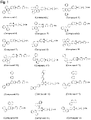
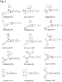
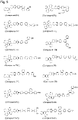
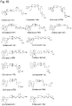
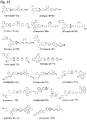
- Figs. 1 to 13 illustrate concrete examples of preferred compounds among compounds having a benzotriazole ring structure represented by the general formulas (a-1) to (a-7) that may be suitably used for the organic EL device of the present invention. Note, however, that the compounds are not limited to the illustrated compounds.
- the compounds having a benzotriazole ring structure of the present invention are novel compounds. These compounds can be synthesized according to a known method as described below, for example (see, for example, Patent Literatures 3 and 5).
- the compound having a benzotriazole ring structure represented by one of general formulas (a-1) to (a-7) can be purified by such techniques as column chromatography purification, adsorption purification with silica gel, activated carbon, activated clay, etc., recrystallization or crystallization using a solvent, sublimation purification, or the like.
- Compound identification can be achieved by NMR analysis.
- Physical properties to be measured preferably include such values as the melting point, glass transition point (Tg), work function, or the like.
- the melting point serves as an index of vapor deposition characteristics.
- the glass transition point (Tg) serves as an index of stability in a thin-film state.
- the work function serves as an index of hole transportability and hole blocking capability.
- the melting point and glass transition point (Tg) can be measured, for example, with a high-sensitivity differential scanning calorimeter (DSC3100SA from Bruker AXS) using a powder.
- DSC3100SA high-sensitivity differential scanning calorimeter
- the work function can be found, for example, with an ionization potential measurement device (PYS-202 from Sumitomo Heavy Industries, Ltd.) by preparing a 100-nm thin film on an ITO substrate.
- PYS-202 ionization potential measurement device
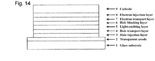
- a structure of the organic EL device of the present invention may, for example, sequentially include, on a substrate, an anode, a hole injection layer, a hole transport layer, a light-emitting layer, an electron transport layer, an electron injection layer, and a cathode.
- an electron blocking layer may be provided between the hole transport layer and the light-emitting layer, or a hole blocking layer may be provided between the light-emitting layer and the electron transport layer.
- a single organic layer may have functions of several layers; for example, a single organic layer may have functions of the hole injection layer and the hole transport layer, or functions of the electron injection layer and the electron transport layer.
- anode in the organic EL device of the present invention it is possible to use an electrode material having a large work function, such as ITO or gold.
- an electrode material having a large work function such as ITO or gold.
- the material for the hole injection layer in the organic EL device of the present invention it is possible to use: a porphyrin compound typified by copper phthalocyanine; a starburst triphenylamine derivative; an arylamine compound including, in its molecule, two or more triphenylamine structures or carbazolyl structures which are linked by a single bond or a divalent group containing no hetero atom; an acceptor heterocyclic compound such as hexacyanoazatriphenylene; or a coating-type polymer material.
- These materials can form thin films by known methods, such as vapor deposition, spin coating, ink-jetting, etc.
- a benzidine derivative such as N,N'-diphenyl-N,N'-di(m-tolyl)-benzidine (abbreviated hereinbelow as "TPD"), N,N'-diphenyl-N,N'-di( ⁇ -naphthyl)-benzidine (abbreviated hereinbelow as "NPD”), N,N,N',N'-tetrabiphenylylbenzidine, etc., or 1,1-bis[(di-4-tolylamino)phenyl]cyclohexane (abbreviated hereinbelow as "TAPC”), or an arylamine compound including, in its molecule, two or more triphenylamine structures or carbazolyl structures which are linked by a single bond or a divalent group containing no hetero atom.
- TPD N,N'-diphenyl-N,N'-di(m-tolyl)-benzidine
- NPD N,N'-dip
- These materials may each be formed into a film singly, or may be mixed with other materials and formed into a film, and each may be used as a single layer. It is possible to form a laminate structure constituted by layers each formed singly by the respective materials, or a laminate structure constituted by layers formed by mixing a plurality of materials, or a laminate structure constituted by layers each formed singly by the respective materials and layers formed by mixing a plurality of materials.
- a coating-type polymer material such as poly(3,4-ethylenedioxythiophene) (abbreviated hereinbelow as “PEDOT”)/poly(styrene sulfonate) (abbreviated hereinbelow as “PSS”).
- PEDOT poly(3,4-ethylenedioxythiophene)
- PSS poly(styrene sulfonate)
- These materials can form thin films by known methods, such as vapor deposition, spin coating, ink-jetting, etc.
- the hole injection layer and the hole transport layer it is possible to use: a material ordinarily used for such layers and p-doped with trisbromophenylamine hexachloroantimonate or a radialene derivative (see, for example, Patent Literature 6); or a polymer compound having, as a partial structure thereof, a benzidine derivative structure such as TPD.
- a compound having an electron blocking action such as: a carbazole derivative, such as 4,4',4"-tri(N-carbazolyl)triphenylamine (abbreviated hereinbelow as "TCTA”), 9,9-bis[4-(carbazol-9-yl)phenyl]fluorene, 1,3-bis(carbazol-9-yl)benzene (abbreviated hereinbelow as "mCP”), 2,2-bis(4-carbazol-9-ylphenyl)adamantane (abbreviated hereinbelow as "Ad-Cz”), etc.; or a compound containing a triarylamine structure and a triphenylsilyl group typified by 9-[4-(carbazol-9-yl)phenyl]-9-[4-(triphenylsilyl)phenyl]-9H-fluorene, etc.
- TCTA 4,4',4"-tri(N-carbazolyl)triphenyl
- These materials may each be formed into a film singly, or may be mixed with other materials and formed into a film, and each may be used as a single layer. It is possible to form a laminate structure constituted by layers each formed singly by the respective materials, or a laminate structure constituted by layers formed by mixing a plurality of materials, or a laminate structure constituted by layers each formed singly by the respective materials and layers formed by mixing a plurality of materials. These materials can form thin films by known methods, such as vapor deposition, spin coating, ink-jetting, etc.
- the material for the light-emitting layer in the organic EL device of the present invention it is possible to use, other than the compound having a benzotriazole ring structure of the present invention, one of various metal complexes such as a metal complex of a quinolinol derivative, e.g., Alq 3 , an anthracene derivative, a bisstyrylbenzene derivative, a pyrene derivative, an oxazole derivative, a poly(para-phenylene vinylene) derivative, etc.
- the light-emitting layer may be constituted by a host material and a dopant material.
- an anthracene derivative may preferably be used, and also, in addition to such light-emitting materials as the compound having a benzotriazole ring structure of the present invention, it is possible to use, for example, a heterocyclic compound having an indole ring as a partial structure of a fused ring, a heterocyclic compound having a carbazole ring as a partial structure of a fused ring, a carbazole derivative, a thiazole derivative, a benzimidazole derivative, a polydialkylfluorene derivative, etc.
- the dopant material it is possible to use quinacridone, coumarin, rubrene, perylene, a derivative of the above, a benzopyran derivative, a rhodamine derivative, an aminostyryl derivative, etc.
- These materials may each be formed into a film singly, or may be mixed with other materials and formed into a film, and each may be used as a single layer. It is possible to form a laminate structure constituted by layers each formed singly by the respective materials, or a laminate structure constituted by layers formed by mixing a plurality of materials, or a laminate structure constituted by layers each formed singly by the respective materials and layers formed by mixing a plurality of materials.
- a phosphorescent substance for the light-emitting material.
- a phosphorescent substance such as a metal complex of iridium, platinum, etc. Examples may include green phosphorescent substances such as Ir(ppy) 3 etc., blue phosphorescent substances such as FIrpic, FIr6, etc., and red phosphorescent substances such as Btp 2 Ir(acac) etc.
- a carbazole derivative such as 4,4'-di(N-carbazolyl) biphenyl (abbreviated hereinbelow as "CBP"), TCTA, mCP, etc., as well as the compound having a benzotriazole ring structure of the present invention.
- CBP 4,4'-di(N-carbazolyl) biphenyl
- TCTA 4,4'-di(N-carbazolyl) biphenyl
- mCP mCP
- TPBI p-bis(triphenylsilyl)benzene
- UH2 p-bis(triphenylsilyl)benzene
- TPBI 2,2',2"-(1,3,5-phenylene)-tris(1-phenyl-1H-benzimidazole)
- doping of the host material(s) with a phosphorescent light-emitting material is preferably performed by co-vapor deposition within a range of 1 to 30 wt.% with respect to the entire light-emitting layer.
- the light-emitting material it is possible to use a material emitting delayed fluorescence, e.g., PIC-TRZ, CC2TA, PXZ-TRZ, a CDCB derivative such as 4CzIPN, etc. (see, for example, Non-Patent Literature 3).
- a material emitting delayed fluorescence e.g., PIC-TRZ, CC2TA, PXZ-TRZ, a CDCB derivative such as 4CzIPN, etc.
- the material for the hole blocking layer in the organic EL device of the present invention it is possible to use, other than the compound having a benzotriazole ring structure of the present invention, a compound having a hole blocking action, with examples including phenanthroline derivatives such as BCP, metal complexes of a quinolinol derivative such as BAlq, various rare-earth complexes, oxazole derivatives, triazole derivatives, triazine derivatives, etc. These materials may also serve as materials for the electron transport layer.
- These materials may each be formed into a film singly, or may be mixed with other materials and formed into a film, and each may be used as a single layer. It is possible to form a laminate structure constituted by layers each formed singly by the respective materials, or a laminate structure constituted by layers formed by mixing a plurality of materials, or a laminate structure constituted by layers each formed singly by the respective materials and layers formed by mixing a plurality of materials. These materials can form thin films by known methods, such as vapor deposition, spin coating, ink-jetting, etc.
- a metal complex of a quinolinol derivative such as Alq 3 , BAlq, etc., one of various metal complexes, a triazole derivative, a triazine derivative, an oxadiazole derivative, a pyridine derivative, a benzimidazole derivative, a thiadiazole derivative, an anthracene derivative, a carbodiimide derivative, a quinoxaline derivative, a pyridoindole derivative, a phenanthroline derivative, a silole derivative, etc.
- a quinolinol derivative such as Alq 3 , BAlq, etc.
- These materials may each be formed into a film singly, or may be mixed with other materials and formed into a film, and each may be used as a single layer. It is possible to form a laminate structure constituted by layers each formed singly by the respective materials, or a laminate structure constituted by layers formed by mixing a plurality of materials, or a laminate structure constituted by layers each formed singly by the respective materials and layers formed by mixing a plurality of materials. These materials can form thin films by known methods, such as vapor deposition, spin coating, ink-jetting, etc.
- an alkali metal salt such as lithium fluoride, cesium fluoride, etc., an alkaline-earth metal salt such as magnesium fluoride etc., a metal complex of a quinolinol derivative such as quinolinol lithium etc., a metal oxide such as aluminum oxide etc., or a metal such as ytterbium (Yb), samarium (Sm), calcium (Ca), strontium (Sr), cesium (Cs), etc.
- the electron injection layer may, however, be omitted by suitable selection of the electron transport layer and the cathode.
- the electron injection layer and the electron transport layer it is possible to use a material ordinarily used for such layers and n-doped with a metal such as cesium etc.
- an electrode material having a low work function such as aluminum etc., or an alloy having an even lower work function, such as magnesium silver alloy, magnesium indium alloy, aluminum magnesium alloy, etc., may be used as the electrode material.
- a reaction vessel was charged with 9.0 g of 2-(4-chloro-phenyl)-5-(9,9'-spirobi[9H]fluoren-2-yl)-2H-benzotriazole, 2.9 g of 4-cyano-phenylboronic acid, 0.5 g of tris(dibenzylideneacetone) dipalladium(0), 0.2 g of tricyclohexyl phosphine, and 10.5 g of tripotassium phosphate, and the mixture was stirred under reflux overnight in a mixed solvent of 1,4-dioxane and H 2 O.
- a reaction vessel was charged with 20.0 g of 2-(4-bromophenyl)-5,6-dichloro-benzotriazole, 18.7 g of 4'-(4,4,5,5-tetramethyl-[1,3,2]dioxaborolan-2-yl)biphenyl-4-carbonitrile, 210 mL of toluene, and 70 mL of ethanol, followed by an aqueous solution made by dissolving, in advance, 9.7 g of potassium carbonate in 70 mL of H 2 O, and was aerated with nitrogen gas for 30 minutes under ultrasonic irradiation.
- the structure of the obtained golden-yellow powder was identified by NMR.
- a reaction vessel was charged with 5.0 g of 2-(4-cyano-[1,1',4',1"]terphenyl-4"-yl)-5,6-dichloro-benzotriazole, 6.2 g of 1-naphthaleneboronic acid, 0.5 g of tris(dibenzylideneacetone)dipalladium(0), 0.6 g of tricyclohexylphosphine, and 14.4 g of tripotassium phosphate, and the mixture was stirred under reflux overnight in a mixed solvent of 1,4-dioxane and H 2 O. After the mixture was allowed to cool, H 2 O was added into the system, and a crude product was obtained by dispersion washing and filtration.
- a reaction vessel was charged with 13.1 g of 5-chloro-2-(4"-cyano-[1,1';4',1"]terphenyl-4-yl)-6-phenyl-2H-benzotriazole, 12.6 g of 9-phenanthreneboronic acid, 1.5 g of tris(dibenzylideneacetone)dipalladium(0), 1.5 g of tricyclohexylphosphine, and 23.0 g of tripotassium phosphate, and the mixture was stirred under reflux overnight in a mixed solvent of 1,4-dioxane and H 2 O. After the mixture was allowed to cool, methanol was added into the system, and a crude product was obtained by dispersion washing and filtration.
- a reaction vessel was charged with 5.6 g of 2-(4-chloro-phenyl)-5-(phenanthren-9-yl)-2H-benzotriazole, 6.2 g of 4'- ⁇ 4-(4,4,5,5-tetramethyl-[1,3,2]dioxaborolan-2-yl)-naphthalen-1-yl ⁇ -biphenyl-4-carbonitrile, 0.4 g of tris(dibenzylideneacetone)dipalladium(0), 0.4 g of tricyclohexylphosphine, and 5.9 g of tripotassium phosphate, and the mixture was stirred under reflux overnight in a mixed solvent of 1,4-dioxane and H 2 O.
- the structure of the obtained pale-yellow powder was identified by NMR.
- a reaction vessel was charged with 26.0 g of 2-(4-bromophenyl)-5-chloro-6-phenyl-benzotriazole, 15.8 g of 9-phenanthreneboronic acid, 180 mL of toluene, and 45 mL of ethanol, followed by an aqueous solution made by dissolving, in advance, 11.2 g of potassium carbonate in 40 mL of H 2 O, and was aerated with nitrogen gas for 30 minutes under ultrasonic irradiation. To the solution aerated with nitrogen gas was added 1.6 g of tetrakistriphenylphosphine palladium, and the mixture was stirred overnight while being heated to reflux.
- the structure of the obtained white powder was identified by NMR.
- a reaction vessel was charged with 10.0 g of 2-(4-chloro-phenyl)-5-(phenanthren-9-yl)-2H-benzotriazole, 9.9 g of 4-(4,4,5,5-tetramethyl-[1,3,2]dioxaborolan-2-yl)-[1,1';4',1"]terphenyl-4"-carbonitrile, 0.7 g of tris(dibenzylideneacetone)dipalladium(0), 0.7 g of tricyclohexylphosphine, and 10.5 g of tripotassium phosphate, and the mixture was stirred under reflux overnight in a mixed solvent of 1,4-dioxane and H 2 O.
- a reaction vessel was charged with 9.0 g of 2-(4-chloro-phenyl)-5-(9,9'-spirobi[9H]fluoren-2-yl)-2H-benzotriazole, 6.5 g of 4- ⁇ 4-(4,4,5,5-tetramethyl-[1,3,2]dioxaborolan-2-yl)-naphthalen-1-yl ⁇ -phenyl-carbonitrile, 0.3 g of tris(dibenzylideneacetone)dipalladium(0), 0.2 g of tricyclohexylphosphine, and 7.0 g of tripotassium phosphate, and the mixture was stirred under reflux overnight in a mixed solvent of 1,4-dioxane and H 2 O.
- the structure of the obtained white powder was identified by NMR.
- a reaction vessel was charged with 12.0 g of 5,6-dichloro-2-[4- ⁇ 4-(4'-cyano-biphenyl-4-yl)-naphthalen-1-yl ⁇ -phenyl]-2H-benzotriazole, 7.7 g of phenylboronic acid, 1.0 g of tris(dibenzylideneacetone)dipalladium(0), 1.2 g of tricyclohexylphosphine, and 26.9 g of tripotassium phosphate, and the mixture was stirred under reflux overnight in a mixed solvent of 1,4-dioxane and H 2 O.
- the structure of the obtained white powder was identified by NMR.
- a reaction vessel was charged with 11.0 g of 5-chloro-2- ⁇ 4-(phenanthren-9-yl)-phenyl ⁇ -2H-benzotriazole, 10.1 g of 4- ⁇ 4-(4,4,5,5-tetramethyl-[1,3,2]dioxaborolan-2-yl)-naphthalen-1-yl ⁇ -phenyl-carbonitrile, 0.7 g of tris(dibenzylideneacetone)dipalladium(0), 0.8 g of tricyclohexylphosphine, and 11.5 g of tripotassium phosphate, and the mixture was stirred under reflux overnight in a mixed solvent of 1,4-dioxane and H 2 O.
- the structure of the obtained pale-yellow powder was identified by NMR.
- a reaction vessel was charged with 10.0 g of 5-chloro-2- ⁇ 4-(phenanthren-9-yl)-phenyl ⁇ -2H-benzotriazole, 11.2 g of 4'- ⁇ 4-(4,4,5,5-tetramethyl-[1,3,2]dioxaborolan-2-yl)-naphthalen-1-yl ⁇ -biphenyl-4-carbonitrile, 0.7 g of tris(dibenzylideneacetone)dipalladium(0), 0.7 g of tricyclohexylphosphine, and 10.5 g of tripotassium phosphate, and the mixture was stirred under reflux overnight in a mixed solvent of 1,4-dioxane and H 2 O.
- a reaction vessel was charged with 13.0 g of 5-chloro-2- ⁇ 4-(phenanthren-9-yl)-phenyl ⁇ -6-phenyl-2H-benzotriazole, 8.6 g of 4-(4,4,5,5-tetramethyl-[1,3,2]dioxaborolan-2-yl)-[1,1';4',1"]terphenyl-4"-carbonitrile, 0.7 g of tris(dibenzylideneacetone)dipalladium(0), 0.8 g of tricyclohexylphosphine, and 11.5 g of tripotassium phosphate, and the mixture was stirred under reflux overnight in a mixed solvent of 1,4-dioxane and H 2 O.
- a reaction vessel was charged with 12.0 g of 5-chloro-6-phenyl-2-(4'-pyridine-3-yl-biphenyl-4-yl)-2H-benzotriazole, 8.4 g of 4'-(4,4,5,5-tetramethyl-[1,3,2]dioxaborolan-2-yl)biphenyl-4-carbonitrile, 0.7 g of tris(dibenzylideneacetone)dipalladium(0), 0.7 g of tricyclohexylphosphine, and 11.1 g of tripotassium phosphate, and the mixture was stirred under reflux overnight in a mixed solvent of 1,4-dioxane and H 2 O.
- the structure of the obtained white powder was identified by NMR.
- a 100-nm-thick vapor deposition film was formed on an ITO substrate by using each of the compounds having a benzotriazole ring structure synthesized respectively in Examples 1 to 13, and the work function was measured using an ionization potential measurement device (PYS-202 from Sumitomo Heavy Industries, Ltd.). The measurement results are collectively shown in Table 2.
- an organic EL device was prepared by vapor-depositing a hole injection layer 3, a hole transport layer 4, a light-emitting layer 5, a hole blocking layer 6, an electron transport layer 7, an electron injection layer 8, and a cathode (aluminum electrode) 9 in this order onto a glass substrate 1 having formed thereon an ITO electrode as a transparent anode 2 in advance.
- a glass substrate 1 having formed thereon a 50-nm-thick ITO film as a transparent anode 2 was subjected to ultrasonic cleaning in isopropyl alcohol for 20 minutes, and then dried for 10 minutes on a hot plate heated to 200°C. Then, after UV ozone treatment for 15 minutes, the glass substrate having the ITO was mounted to a vacuum vapor deposition apparatus, in which the pressure was reduced to 0.001 Pa or lower.
- a hole injection layer 3 was formed as the film of 10 nm thickness so as to cover the transparent anode 2, by performing binary vapor deposition of an electron acceptor (Acceptor-1) having the following structural formula and a compound (HTM-1) having the following structural formula at a rate at which the vapor deposition rate ratio between Acceptor-1 and HTM-1 was 3:97.
- an electron acceptor (Acceptor-1) having the following structural formula
- HTM-1 compound having the following structural formula
- the compound (HTM-1) having the following structural formula was formed as a hole transport layer 4 having a film thickness of 60 nm.
- a light-emitting layer 5 was formed so that the film thickness was 20 nm, by performing binary vapor deposition of a compound (EMD-1) having the following structural formula and a compound (EMH-1) having the following structural formula at a rate at which the vapor deposition rate ratio between EMD-1 and EMH-1 was 5:95.
- a hole blocking layer- cum- electron transport layer 6, 7 was formed by performing binary vapor deposition of the compound of Example 1 (Compound-2) and a compound (ETM-1) having the following structural formula at a rate at which the vapor deposition rate ratio between Compound-2 and ETM-1 was 50:50, to the film thickness of 30nm.
- lithium fluoride was formed as an electron injection layer 8 having a film thickness of 1 nm.
- a cathode 9 was formed by vapor-depositing aluminum to a thickness of 100 nm.
- An organic EL device was produced according to the same conditions in Example 16, except that, the compound (Compound-40) of Example 2 was used instead of the compound (Compound-2) of Example 1 as the material for the hole blocking layer- cum- electron transport layer 6, 7, and binary vapor deposition was performed at a vapor deposition rate at which the vapor deposition rate ratio between Compound-40 and ETM-1 was 50:50.
- Properties of the produced organic EL device were measured in the atmosphere at atmospheric temperature. Measurement results of light emission properties when a direct-current voltage was applied to the produced organic EL device are collectively shown in Table 3.
- An organic EL device was produced according to the same conditions in Example 16, except that, the compound (Compound-44) of Example 3 was used instead of the compound (Compound-2) of Example 1 as the material for the hole blocking layer- cum- electron transport layer 6, 7, and binary vapor deposition was performed at a vapor deposition rate at which the vapor deposition rate ratio between Compound-44 and ETM-1 was 50:50.
- Properties of the produced organic EL device were measured in the atmosphere at atmospheric temperature. Measurement results of light emission properties when a direct-current voltage was applied to the produced organic EL device are collectively shown in Table 3.
- An organic EL device was produced according to the same conditions in Example 16, except that, the compound (Compound-48) of Example 4 was used instead of the compound (Compound-2) of Example 1 as the material for the hole blocking layer- cum- electron transport layer 6, 7, and binary vapor deposition was performed at a vapor deposition rate at which the vapor deposition rate ratio between Compound-48 and ETM-1 was 50:50.
- Properties of the produced organic EL device were measured in the atmosphere at atmospheric temperature. Measurement results of light emission properties when a direct-current voltage was applied to the produced organic EL device are collectively shown in Table 3.
- An organic EL device was produced according to the same conditions in Example 16, except that, the compound (Compound-78) of Example 5 was used instead of the compound (Compound-2) of Example 1 as the material for the hole blocking layer- cum- electron transport layer 6, 7, and binary vapor deposition was performed at a vapor deposition rate at which the vapor deposition rate ratio between Compound-78 and ETM-1 was 50:50.
- Properties of the produced organic EL device were measured in the atmosphere at atmospheric temperature. Measurement results of light emission properties when a direct-current voltage was applied to the produced organic EL device are collectively shown in Table 3.
- An organic EL device was produced according to the same conditions in Example 16, except that, the compound (Compound-104) of Example 6 was used instead of the compound (Compound-2) of Example 1 as the material for the hole blocking layer- cum- electron transport layer 6, 7, and binary vapor deposition was performed at a vapor deposition rate at which the vapor deposition rate ratio between Compound-104 and ETM-1 was 50:50.
- Properties of the produced organic EL device were measured in the atmosphere at atmospheric temperature. Measurement results of light emission properties when a direct-current voltage was applied to the produced organic EL device are collectively shown in Table 3.
- An organic EL device was produced according to the same conditions in Example 16 , except that, the compound (Compound-141) of Example 7 was used instead of the compound (Compound-2) of Example 1 as the material for the hole blocking layer- cum- electron transport layer 6, 7, and binary vapor deposition was performed at a vapor deposition rate at which the vapor deposition rate ratio between Compound-141 and ETM-1 was 50:50.
- Properties of the produced organic EL device were measured in the atmosphere at atmospheric temperature. Measurement results of light emission properties when a direct-current voltage was applied to the produced organic EL device are collectively shown in Table 3.
- An organic EL device was produced according to the same conditions in Example 16, except that, the compound (Compound-155) of Example 8 was used instead of the compound (Compound-2) of Example 1 as the material for the hole blocking layer- cum- electron transport layer 6, 7, and binary vapor deposition was performed at a vapor deposition rate at which the vapor deposition rate ratio between Compound-155 and ETM-1 was 50:50.
- Properties of the produced organic EL device were measured in the atmosphere at atmospheric temperature. Measurement results of light emission properties when a direct-current voltage was applied to the produced organic EL device are collectively shown in Table 3.
- An organic EL device was produced according to the same conditions in Example 16, except that, the compound (Compound-164) of Example 9 was used instead of the compound (Compound-2) of Example 1 as the material for the hole blocking layer- cum- electron transport layer 6, 7, and binary vapor deposition was performed at a vapor deposition rate at which the vapor deposition rate ratio between Compound-164 and ETM-1 was 50:50.
- Properties of the produced organic EL device were measured in the atmosphere at atmospheric temperature. Measurement results of light emission properties when a direct-current voltage was applied to the produced organic EL device are collectively shown in Table 3.
- An organic EL device was produced according to the same conditions in Example 16, except that, the compound (Compound-172) of Example 10 was used instead of the compound (Compound-2) of Example 1 as the material for the hole blocking layer- cum- electron transport layer 6, 7, and binary vapor deposition was performed at a vapor deposition rate at which the vapor deposition rate ratio between Compound-172 and ETM-1 was 50:50.
- Properties of the produced organic EL device were measured in the atmosphere at atmospheric temperature. Measurement results of light emission properties when a direct-current voltage was applied to the produced organic EL device are collectively shown in Table 3.
- An organic EL device was produced according to the same conditions in Example 16, except that, the compound (Compound-184) of Example 11 was used instead of the compound (Compound-2) of Example 1 as the material for the hole blocking layer- cum- electron transport layer 6, 7, and binary vapor deposition was performed at a vapor deposition rate at which the vapor deposition rate ratio between Compound-184 and ETM-1 was 50:50.
- Properties of the produced organic EL device were measured in the atmosphere at atmospheric temperature. Measurement results of light emission properties when a direct-current voltage was applied to the produced organic EL device are collectively shown in Table 3.
- An organic EL device was produced according to the same conditions in Example 16 , except that, the compound (Compound-189) of Example 12 was used instead of the compound (Compound-2) of Example 1 as the material for the hole blocking layer- cum- electron transport layer 6, 7, and binary vapor deposition was performed at a vapor deposition rate at which the vapor deposition rate ratio between Compound-189 and ETM-1 was 50:50.
- Properties of the produced organic EL device were measured in the atmosphere at atmospheric temperature. Measurement results of light emission properties when a direct-current voltage was applied to the produced organic EL device are collectively shown in Table 3.
- An organic EL device was produced according to the same conditions in Example 16, except that, the compound (Compound-201) of Example 13 was used instead of the compound (Compound-2) of Example 1 as the material for the hole blocking layer- cum- electron transport layer 6, 7, and binary vapor deposition was performed at a vapor deposition rate at which the vapor deposition rate ratio between Compound-201 and ETM-1 was 50:50.
- Properties of the produced organic EL device were measured in the atmosphere at atmospheric temperature. Measurement results of light emission properties when a direct-current voltage was applied to the produced organic EL device are collectively shown in Table 3.
- Comparative Example 1 For comparison, an organic EL device was produced according to the same conditions in Example 16, except that, a compound (ETM-2) having the following structural formula (see, for example, Patent Literature 7) was used instead of the compound (Compound-2) of Example 1 as the material for the hole blocking layer- cum- electron transport layer 6, 7, and binary vapor deposition was performed at a vapor deposition rate at which the vapor deposition rate ratio between ETM-2 and ETM-1 was 50:50.
- Properties of the produced organic EL device were measured in the atmosphere at atmospheric temperature. Measurement results of light emission properties when a direct-current voltage was applied to the produced organic EL device are collectively shown in Table 3.
- Comparative Example 2 For comparison, an organic EL device was produced according to the same conditions in Example 16, except that, a compound (ETM-3) having the following structural formula (see, for example, Patent Literature 8) was used instead of the compound (Compound-2) of Example 1 as the material for the hole blocking layer- cum- electron transport layer 6, 7, and binary vapor deposition was performed at a vapor deposition rate at which the vapor deposition rate ratio between ETM-3 and ETM-1 was 50:50.
- Properties of the produced organic EL device were measured in the atmosphere at atmospheric temperature. Measurement results of light emission properties when a direct-current voltage was applied to the produced organic EL device are collectively shown in Table 3.
- Device life was measured using the organic EL devices produced in Examples 16 to 28 and Comparative Examples 1 and 2. The results are collectively shown in Table 3. Device life was measured as following, constant current driving was performed with the light emission luminance at the start of light emission (i.e., initial luminance) being 2000 cd/m 2 , and then the time for the light emission luminance attenuating to 1900 cd/m 2 (95% attenuation: the equivalent of 95% of the initial luminance, that considering to be 100%) was measured.
- the organic EL devices of Comparative Examples 1 and 2 had a power efficiency of 5.16 to 6.62 lm/W
- the organic EL devices of Comparative Examples 1 and 2 had a device life (95% attenuation) of 165 to 203 hours
- the organic EL devices according to the present invention excelled in luminous efficiency and power efficiency, compared to devices using compounds ETM-2 and ETM-3 having the structural formulas shown above, and it could achieve organic EL devices with a long lifetime.
- Compounds having a specific benzotriazole ring structure according to the present invention have good electron injection capability and excellent hole blocking capability and are stable in a thin film state and are thus excellent for organic EL devices.
- organic EL devices By producing organic EL devices using these compounds, high efficiency can be achieved, driving voltage can be reduced, and durability can be improved also. For example, application can be expanded to home electrical appliances and lightings.
Applications Claiming Priority (2)
| Application Number | Priority Date | Filing Date | Title |
|---|---|---|---|
| JP2019106028 | 2019-06-06 | ||
| PCT/JP2020/021845 WO2020246484A1 (fr) | 2019-06-06 | 2020-06-02 | Composé à structure cyclique de type benzotriazole et élément électroluminescent organique |
Publications (1)
| Publication Number | Publication Date |
|---|---|
| EP3981764A1 true EP3981764A1 (fr) | 2022-04-13 |
Family
ID=73653186
Family Applications (1)
| Application Number | Title | Priority Date | Filing Date |
|---|---|---|---|
| EP20818227.9A Withdrawn EP3981764A1 (fr) | 2019-06-06 | 2020-06-02 | Composé à structure cyclique de type benzotriazole et élément électroluminescent organique |
Country Status (7)
| Country | Link |
|---|---|
| US (1) | US20220220083A1 (fr) |
| EP (1) | EP3981764A1 (fr) |
| JP (1) | JPWO2020246484A1 (fr) |
| KR (1) | KR20220018474A (fr) |
| CN (1) | CN113795481A (fr) |
| TW (1) | TW202106668A (fr) |
| WO (1) | WO2020246484A1 (fr) |
Families Citing this family (1)
| Publication number | Priority date | Publication date | Assignee | Title |
|---|---|---|---|---|
| CN116249360B (zh) * | 2022-12-30 | 2023-11-14 | 深圳职业技术学院 | 一种有机太阳能电池及其制备方法 |
Family Cites Families (12)
| Publication number | Priority date | Publication date | Assignee | Title |
|---|---|---|---|---|
| US2972611A (en) * | 1961-02-21 | Irrttnrpsrumttuiatotvt stttkvnf | ||
| CH562227A5 (fr) * | 1971-05-26 | 1975-05-30 | Sandoz Ag | |
| US5869199A (en) | 1993-03-26 | 1999-02-09 | Sumitomo Electric Industries, Ltd. | Organic electroluminescent elements comprising triazoles |
| DE69412567T2 (de) | 1993-11-01 | 1999-02-04 | Hodogaya Chemical Co Ltd | Aminverbindung und sie enthaltende Elektrolumineszenzvorrichtung |
| EP0666298A3 (fr) | 1994-02-08 | 1995-11-15 | Tdk Corp | Elément organique électroluminescent et composé utilisé. |
| KR100691543B1 (ko) | 2002-01-18 | 2007-03-09 | 주식회사 엘지화학 | 새로운 전자 수송용 물질 및 이를 이용한 유기 발광 소자 |
| US20080027226A1 (en) | 2003-12-05 | 2008-01-31 | Jonathan Rogers | Electroluminescent Device |
| KR101288557B1 (ko) | 2008-12-24 | 2013-07-22 | 제일모직주식회사 | 신규한 유기광전소자용 화합물 및 이를 포함하는 유기광전소자 |
| KR20120051598A (ko) * | 2010-11-12 | 2012-05-22 | 주식회사 엘지화학 | 신규한 화합물 및 이를 이용한 유기 전자 소자 |
| KR102083691B1 (ko) * | 2011-10-14 | 2020-03-02 | 호도가야 가가쿠 고교 가부시키가이샤 | 신규 벤조트리아졸 유도체 및 그 유도체가 사용되는 유기 전계 발광 소자 |
| EP2684932B8 (fr) | 2012-07-09 | 2016-12-21 | Hodogaya Chemical Co., Ltd. | Matériau de matrice dopé avec une composé mesomeric radialène |
| JP6701498B2 (ja) * | 2016-07-20 | 2020-05-27 | エルジー・ケム・リミテッド | 新規なヘテロ環式化合物およびこれを利用した有機発光素子 |
-
2020
- 2020-06-02 JP JP2021524865A patent/JPWO2020246484A1/ja active Pending
- 2020-06-02 WO PCT/JP2020/021845 patent/WO2020246484A1/fr active Application Filing
- 2020-06-02 EP EP20818227.9A patent/EP3981764A1/fr not_active Withdrawn
- 2020-06-02 CN CN202080033772.9A patent/CN113795481A/zh active Pending
- 2020-06-02 US US17/609,097 patent/US20220220083A1/en active Pending
- 2020-06-02 KR KR1020217034861A patent/KR20220018474A/ko unknown
- 2020-06-04 TW TW109118757A patent/TW202106668A/zh unknown
Also Published As
| Publication number | Publication date |
|---|---|
| WO2020246484A1 (fr) | 2020-12-10 |
| TW202106668A (zh) | 2021-02-16 |
| US20220220083A1 (en) | 2022-07-14 |
| CN113795481A (zh) | 2021-12-14 |
| KR20220018474A (ko) | 2022-02-15 |
| JPWO2020246484A1 (fr) | 2020-12-10 |
Similar Documents
| Publication | Publication Date | Title |
|---|---|---|
| EP3156402A1 (fr) | Dérivé de pyrimidine et élément électroluminescent organique | |
| EP3664173B1 (fr) | Élément électroluminescent organique contenant un composé présentant une structure cyclique de benzoazole | |
| JP7227141B2 (ja) | 有機エレクトロルミネッセンス素子 | |
| EP3925958A1 (fr) | Composé possédant une structure cyclique de benzoazole, et élément électroluminescent organique | |
| JP7394050B2 (ja) | ベンゾイミダゾール環構造を有する化合物および有機エレクトロルミネッセンス素子 | |
| EP4112613A1 (fr) | Composé arylamine et dispositif électronique l'utilisant | |
| JP7369714B2 (ja) | アザベンゾオキサゾール環構造を有する化合物および有機エレクトロルミネッセンス素子 | |
| EP3981764A1 (fr) | Composé à structure cyclique de type benzotriazole et élément électroluminescent organique | |
| EP4230615A1 (fr) | Composé arylamine, élément électroluminescent organique et dispositif électronique | |
| JP7406500B2 (ja) | ピリミジン環構造を有する化合物および有機エレクトロルミネッセンス素子 | |
| JP7159173B2 (ja) | ピリミジン環構造を有する化合物および有機エレクトロルミネッセンス素子 | |
| EP4095124A1 (fr) | Composé arylamine et élément électroluminescent organique | |
| WO2019039402A1 (fr) | Composé ayant une structure cyclique d'indéobenzoazole, et élément électroluminescent organique |
Legal Events
| Date | Code | Title | Description |
|---|---|---|---|
| STAA | Information on the status of an ep patent application or granted ep patent |
Free format text: STATUS: THE INTERNATIONAL PUBLICATION HAS BEEN MADE |
|
| PUAI | Public reference made under article 153(3) epc to a published international application that has entered the european phase |
Free format text: ORIGINAL CODE: 0009012 |
|
| STAA | Information on the status of an ep patent application or granted ep patent |
Free format text: STATUS: REQUEST FOR EXAMINATION WAS MADE |
|
| 17P | Request for examination filed |
Effective date: 20211025 |
|
| AK | Designated contracting states |
Kind code of ref document: A1 Designated state(s): AL AT BE BG CH CY CZ DE DK EE ES FI FR GB GR HR HU IE IS IT LI LT LU LV MC MK MT NL NO PL PT RO RS SE SI SK SM TR |
|
| DAV | Request for validation of the european patent (deleted) | ||
| DAX | Request for extension of the european patent (deleted) | ||
| STAA | Information on the status of an ep patent application or granted ep patent |
Free format text: STATUS: THE APPLICATION HAS BEEN WITHDRAWN |
|
| 18W | Application withdrawn |
Effective date: 20230302 |