EP3972130A1 - Wafer-level surface acoustic wave filter and packaging method - Google Patents
Wafer-level surface acoustic wave filter and packaging method Download PDFInfo
- Publication number
- EP3972130A1 EP3972130A1 EP21802176.4A EP21802176A EP3972130A1 EP 3972130 A1 EP3972130 A1 EP 3972130A1 EP 21802176 A EP21802176 A EP 21802176A EP 3972130 A1 EP3972130 A1 EP 3972130A1
- Authority
- EP
- European Patent Office
- Prior art keywords
- layer
- material layer
- cover plate
- thin film
- piezoelectric thin
- Prior art date
- Legal status (The legal status is an assumption and is not a legal conclusion. Google has not performed a legal analysis and makes no representation as to the accuracy of the status listed.)
- Withdrawn
Links
Images



Classifications
-
- H—ELECTRICITY
- H03—ELECTRONIC CIRCUITRY
- H03H—IMPEDANCE NETWORKS, e.g. RESONANT CIRCUITS; RESONATORS
- H03H9/00—Networks comprising electromechanical or electro-acoustic elements; Electromechanical resonators
- H03H9/02—Details
- H03H9/05—Holders or supports
- H03H9/10—Mounting in enclosures
- H03H9/1064—Mounting in enclosures for surface acoustic wave [SAW] devices
-
- H—ELECTRICITY
- H03—ELECTRONIC CIRCUITRY
- H03H—IMPEDANCE NETWORKS, e.g. RESONANT CIRCUITS; RESONATORS
- H03H9/00—Networks comprising electromechanical or electro-acoustic elements; Electromechanical resonators
- H03H9/02—Details
- H03H9/05—Holders or supports
- H03H9/10—Mounting in enclosures
- H03H9/1064—Mounting in enclosures for surface acoustic wave [SAW] devices
- H03H9/1092—Mounting in enclosures for surface acoustic wave [SAW] devices the enclosure being defined by a cover cap mounted on an element forming part of the surface acoustic wave [SAW] device on the side of the IDT's
-
- H—ELECTRICITY
- H03—ELECTRONIC CIRCUITRY
- H03H—IMPEDANCE NETWORKS, e.g. RESONANT CIRCUITS; RESONATORS
- H03H3/00—Apparatus or processes specially adapted for the manufacture of impedance networks, resonating circuits, resonators
- H03H3/007—Apparatus or processes specially adapted for the manufacture of impedance networks, resonating circuits, resonators for the manufacture of electromechanical resonators or networks
- H03H3/08—Apparatus or processes specially adapted for the manufacture of impedance networks, resonating circuits, resonators for the manufacture of electromechanical resonators or networks for the manufacture of resonators or networks using surface acoustic waves
-
- H—ELECTRICITY
- H03—ELECTRONIC CIRCUITRY
- H03H—IMPEDANCE NETWORKS, e.g. RESONANT CIRCUITS; RESONATORS
- H03H9/00—Networks comprising electromechanical or electro-acoustic elements; Electromechanical resonators
- H03H9/02—Details
- H03H9/02535—Details of surface acoustic wave devices
- H03H9/02543—Characteristics of substrate, e.g. cutting angles
- H03H9/02574—Characteristics of substrate, e.g. cutting angles of combined substrates, multilayered substrates, piezoelectrical layers on not-piezoelectrical substrate
-
- H—ELECTRICITY
- H03—ELECTRONIC CIRCUITRY
- H03H—IMPEDANCE NETWORKS, e.g. RESONANT CIRCUITS; RESONATORS
- H03H9/00—Networks comprising electromechanical or electro-acoustic elements; Electromechanical resonators
- H03H9/02—Details
- H03H9/02535—Details of surface acoustic wave devices
- H03H9/02818—Means for compensation or elimination of undesirable effects
- H03H9/02834—Means for compensation or elimination of undesirable effects of temperature influence
-
- H—ELECTRICITY
- H03—ELECTRONIC CIRCUITRY
- H03H—IMPEDANCE NETWORKS, e.g. RESONANT CIRCUITS; RESONATORS
- H03H9/00—Networks comprising electromechanical or electro-acoustic elements; Electromechanical resonators
- H03H9/02—Details
- H03H9/05—Holders or supports
- H03H9/058—Holders or supports for surface acoustic wave devices
- H03H9/059—Holders or supports for surface acoustic wave devices consisting of mounting pads or bumps
-
- H—ELECTRICITY
- H03—ELECTRONIC CIRCUITRY
- H03H—IMPEDANCE NETWORKS, e.g. RESONANT CIRCUITS; RESONATORS
- H03H9/00—Networks comprising electromechanical or electro-acoustic elements; Electromechanical resonators
- H03H9/02—Details
- H03H9/05—Holders or supports
- H03H9/10—Mounting in enclosures
- H03H9/1064—Mounting in enclosures for surface acoustic wave [SAW] devices
- H03H9/1071—Mounting in enclosures for surface acoustic wave [SAW] devices the enclosure being defined by a frame built on a substrate and a cap, the frame having no mechanical contact with the SAW device
-
- H—ELECTRICITY
- H03—ELECTRONIC CIRCUITRY
- H03H—IMPEDANCE NETWORKS, e.g. RESONANT CIRCUITS; RESONATORS
- H03H9/00—Networks comprising electromechanical or electro-acoustic elements; Electromechanical resonators
- H03H9/15—Constructional features of resonators consisting of piezoelectric or electrostrictive material
-
- H—ELECTRICITY
- H03—ELECTRONIC CIRCUITRY
- H03H—IMPEDANCE NETWORKS, e.g. RESONANT CIRCUITS; RESONATORS
- H03H9/00—Networks comprising electromechanical or electro-acoustic elements; Electromechanical resonators
- H03H9/46—Filters
- H03H9/64—Filters using surface acoustic waves
-
- H—ELECTRICITY
- H03—ELECTRONIC CIRCUITRY
- H03H—IMPEDANCE NETWORKS, e.g. RESONANT CIRCUITS; RESONATORS
- H03H9/00—Networks comprising electromechanical or electro-acoustic elements; Electromechanical resonators
- H03H9/46—Filters
- H03H9/64—Filters using surface acoustic waves
- H03H9/6423—Means for obtaining a particular transfer characteristic
-
- H—ELECTRICITY
- H10—SEMICONDUCTOR DEVICES; ELECTRIC SOLID-STATE DEVICES NOT OTHERWISE PROVIDED FOR
- H10W—GENERIC PACKAGES, INTERCONNECTIONS, CONNECTORS OR OTHER CONSTRUCTIONAL DETAILS OF DEVICES COVERED BY CLASS H10
- H10W70/00—Package substrates; Interposers; Redistribution layers [RDL]
- H10W70/60—Insulating or insulated package substrates; Interposers; Redistribution layers
- H10W70/62—Insulating or insulated package substrates; Interposers; Redistribution layers characterised by their interconnections
- H10W70/63—Vias, e.g. via plugs
- H10W70/635—Through-vias
-
- H—ELECTRICITY
- H10—SEMICONDUCTOR DEVICES; ELECTRIC SOLID-STATE DEVICES NOT OTHERWISE PROVIDED FOR
- H10W—GENERIC PACKAGES, INTERCONNECTIONS, CONNECTORS OR OTHER CONSTRUCTIONAL DETAILS OF DEVICES COVERED BY CLASS H10
- H10W90/00—Package configurations
- H10W90/701—Package configurations characterised by the relative positions of pads or connectors relative to package parts
Definitions
- Embodiments of the present application relate to the technical field of semiconductor, and in particular, to a wafer level surface acoustic wave filter and a package method.
- a surface acoustic wave filter has characteristics of high working frequency, wide band pass, good frequency selection characteristics, small size and light weight, and it can use the same production process as an integrated circuit, with easy manufacture, low cost, and good consistent frequency characteristics, and therefore, it is widely used in various electronic devices.
- CA Carrier Aggregation
- QAM Quadrature Amplitude Modulation
- the number of RF front-end components has not only increased substantially, but also increasingly stringent technical requirements have been put forward for the performance of filter components, for example, it is required to have better temperature stability and a smaller package size, in order to be highly integrated with an active device such as a power amplifier and an RF switch in the RF front-end. Therefore, how to design a filter component with smaller size and higher stability is an urgent problem to be solved.
- Embodiments of the present application provide a wafer level surface acoustic wave filter and a package method, which can effectively improve the temperature stability of the surface acoustic wave filter and reduce the size of the surface acoustic wave filter.
- a wafer level surface acoustic wave filter including: a wafer, an electrode layer, a supporting wall and a cover plate; where the wafer includes a substrate layer and a piezoelectric thin film layer, and the substrate layer and the piezoelectric thin film layer are combined together by wafer bonding therebetween.
- the electrode layer is arranged on a surface of the piezoelectric thin film layer, the supporting wall is located between the piezoelectric thin film layer and the cover plate, and the supporting wall surrounds between the piezoelectric thin film layer and the cover plate to form a sealed cavity.
- the cover plate includes at least a first material layer, and the first material layer uses the same material as the substrate layer.
- a ratio of a thickness of the piezoelectric thin film layer to a thickness of the wafer is less than a preset threshold.
- a value of the preset threshold is 0.1.
- the cover plate includes at least two material layers, and a thickness of each material layer is related to a temperature expansion coefficient of each material layer.
- the cover plate includes the first material layer and a second material layer, the first material layer and the second material layer are combined together by wafer bonding therebetween; the second material layer is located on a side of the cover plate close to the sealed cavity; and the second material layer uses the same material as the piezoelectric thin film layer.
- the cover plate includes the first material layer, a second material layer and a third material layer; the third material layer is located between the first material layer and the second material layer, and the first material layer and the second material layer are combined together by using the third material layer; the second material layer is located on a side of the cover plate close to the sealed cavity; and the second material layer uses the same material as the piezoelectric thin film layer.
- a material used for the third material layer is an organic binder.
- the electrode layer includes an interdigital electrode and a thickened electrode, and the thickened electrode is distributed in at least one of following positions of the interdigital electrode: an input position, an output position, and an earthing position.
- solder ball penetrates the cover plate and the supporting wall in a through silicon via (TSV) manner and then electrically contacts the electrode layer; or, the solder ball is electrically connected with the electrode layer in a redistribution layer (RDL) manner.
- TSV through silicon via
- RDL redistribution layer
- the piezoelectric thin film layer is made from at least one of following materials: lithium tantalate LiTaO 3 and lithium niobate LiNbO 3 .
- the substrate layer is made from at least one of following materials: silicon Si and sapphire.
- embodiments of the present application provide a package method for a wafer level surface acoustic wave filter, including:
- a ratio of a thickness of the piezoelectric thin film layer to a thickness of the wafer is less than a preset threshold.
- a value of the preset threshold is 0.1.
- the cover plate includes at least two material layers, and a thickness of each material layer is related to a temperature expansion coefficient of each material layer.
- the cover plate includes the first material layer and a second material layer, the first material layer and the second material layer are combined together by wafer bonding therebetween, and the second material layer uses the same material as the piezoelectric thin film layer.
- the cover plate includes the first material layer, a second material layer and a third material layer; the third material layer is located between the first material layer and the second material layer, and the first material layer and the second material layer are combined together by using the third material layer; and the second material layer uses the same material as the piezoelectric thin film layer.
- the package method further includes: forming a via hole which penetrates the cover plate and the supporting wall in a through silicon via (TSV) manner at a preset position of the cover plate, and implanting a solder ball in the via hole by electroplating, the solder ball electrically contacting the electrode layer.
- TSV through silicon via
- Embodiments of the present application provide a wafer level surface acoustic wave filter and a package method
- the surface acoustic wave filter includes a wafer, an electrode layer, a supporting wall and a cover plate; where, the wafer includes a substrate layer and a piezoelectric thin film layer combined together by wafer bonding, the electrode layer is arranged on a surface of the piezoelectric thin film layer, the supporting wall is located between the piezoelectric thin film layer and the cover plate, and the supporting wall surrounds between the piezoelectric thin film layer and the cover plate to form a sealed cavity; the cover plate includes at least a first material layer, which uses the same material as the substrate layer.
- the size of the surface acoustic wave filter can be effectively reduced; the substrate layer and the piezoelectric thin film layer are combined together by wafer bonding, the performance of the surface acoustic wave filter based on this type of wafer is less affected by temperature; and the cover plate uses the same or similar material as the wafer, which can enhance the reliability and temperature stability of a device.
- the package of existing surface acoustic wave filters is mostly completed by etching substrate material of chips, which is difficult to process, and it is difficult to meet the current requirements for the size and stability of surface acoustic wave filters.
- an embodiment of the present application provides a wafer level surface acoustic wave filter
- the use of wafer level package can effectively reduce the size of the surface acoustic wave filter, which can be suitable for packaging RF front-end module; additionally, the substrate layer and the piezoelectric thin film layer are combined together by wafer bonding, which can improve the temperature stability of the surface acoustic wave filter; and, the cover plate uses the same or similar material as the substrate layer, thereby further enhancing the reliability of the surface acoustic wave filter, and reducing the influence of temperature changes on the surface acoustic wave filter.
- the present application is described in detail through the following examples.
- FIG. 1 is a schematic top view of a package structure of a wafer level surface acoustic wave filter in an embodiment of the present application.
- a package structure 100 of the abovementioned surface acoustic wave filter includes a number of solder balls 101.
- the package structure can be applied to the wafer-level package of the surface acoustic wave filter, so as to achieve the protection of a working surface of the surface acoustic wave filter and the extraction of electrodes.
- a number of surface acoustic wave filter components can be obtained by cutting.
- FIG. 2 is a schematic sectional view I of a package structure of a surface acoustic wave filter taken along a section line AB shown in FIG. 1 .
- the section shown in FIG. 2 can be considered as a schematic view of a cross-sectional structure of a surface acoustic wave filter.
- the surface acoustic wave filter includes a wafer, an electrode layer, a supporting wall 205 and a cover plate.
- the abovementioned wafer includes a substrate layer 201 and a piezoelectric thin film layer 202, and the substrate layer 201 and the piezoelectric thin film layer 202 are combined together by wafer bonding therebetween. Since a thickness of the piezoelectric thin film layer 202 is less than a preset threshold, the temperature expansion coefficient of the wafer after bonding is close to the temperature expansion coefficient of the substrate layer 201.
- each material layer of the surface acoustic wave filter shown in FIG. 2 is only for exemplary illustration, and does not represent an actual thickness.
- a way of wafer bonding means that two mirror-polished homogenous or heterogeneous wafers are closely combined through chemical and physical action. After the wafers are bonded, atoms at the interface are subjected to external forces to react, so as to form covalent bonds for combining together, so that a bonding interface reaches a specific bonding strength.
- the use of wafer bonding way is conducive to achieving a low temperature drift and improving the power tolerance performance of the surface acoustic wave filter.
- the abovementioned electrode layer includes an interdigital electrode 203 and a thickened electrode 204, and the thickened electrode 204 is distributed in at least one of following positions of the interdigital electrode 203: an input position, an output position, and an earthing position.
- the abovementioned interdigital electrode 203 is arranged on a surface of the piezoelectric thin film layer 202.
- the interdigital electrode 203 and the thickened electrode 204 can be formed on the surface of the piezoelectric thin film layer 102 by photoetching method.
- the supporting wall 205 is located between the piezoelectric thin film layer 202 and the cover plate, and the supporting wall 205 surrounds between the piezoelectric thin film layer 202 and the cover plate to form a sealed cavity 207.
- the cover plate can include only one layer of material, i.e., a first material layer 206, and the first material layer 206 uses the same material as the substrate layer 201.
- the substrate layer 201 can be made from silicon Si and sapphire, etc., with a thickness of 30 ⁇ 150 ⁇ .
- the piezoelectric thin film layer 202 can be made from film material with piezoelectric performance, such as lithium tantalate LiTaO 3 and lithium niobate LiNbO 3 , etc., with a thickness of 0.05 ⁇ 15 ⁇ .
- the substrate layer 201 and the piezoelectric thin film layer 202 can be a combination of the following materials: LiTaO 3 and Si, LiNbO 3 and Si, LiTaO 3 and sapphire, LiNbO 3 and sapphire.
- the electrode layer can be made from aluminum, copper, gold, aluminum-copper alloy, etc., with a thickness of 6% ⁇ 15% ⁇ , where ⁇ is a wavelength of a surface acoustic wave.
- the supporting wall 205 can be made from viscous materials, which can surround the electrode layer.
- a ratio of a thickness of the piezoelectric thin film layer to that of the wafer is less than a preset threshold.
- a ratio of the thickness of the piezoelectric thin film layer to that of the wafer is less than 0.1.
- the LiTaO 3 or LiNbO 3 used in the piezoelectric thin film layer 202 has a relatively large temperature expansion coefficient
- a formed filter device has a relatively large frequency drift.
- the frequency drift of the filter device can be effectively reduced.
- the thickness of the piezoelectric thin film layer 202 can be set below 20 um, and the thickness of the substrate layer 201 can be set at about 230 um.
- the piezoelectric thin film layer 202 is relatively thin, and has a relatively small contribution to the temperature expansion coefficient of the entire wafer, thus, only a single layer of material same as a substrate material can be used to make the cover plate, so that the temperature expansion coefficient of the cover plate can be close to the temperature expansion coefficient of the wafer.
- the temperature when the temperature changes, it can prevent deformation of the cover plate and the wafer in different magnitudes due to a large difference between the temperature expansion coefficient of the cover plate and the temperature expansion coefficient of the wafer, which damages the sealed cavity 207. It reduces the influence of temperature changes on the surface acoustic wave filter, thereby effectively enhancing the reliability of the surface acoustic wave filter.
- the use of wafer level package can effectively reduce the size of the surface acoustic wave filter, which can be suitable for the application in packaging RF front-end module; additionally, the substrate layer and the piezoelectric thin film layer are combined together by wafer bonding, thus the performance of the surface acoustic wave filter based on this type of wafer is less affected by temperature; and the cover plate uses the same material as the substrate layer, thereby also enhancing the overall reliability of the surface acoustic wave filter, and further reducing the influence of temperature changes on the surface acoustic wave filter.
- the abovementioned cover plate includes at least two material layers, the thickness of each material layer can be flexibly set according to the temperature expansion coefficient of each material layer, so as to reduce the influence of external temperature changes on the entire surface acoustic wave filter.
- FIG. 3 is a schematic sectional view II of a package structure of a surface acoustic wave filter taken along a section line AB shown in FIG. 1 .
- the section shown in FIG. 3 can be considered as a schematic view of a cross-sectional structure of a surface acoustic wave filter.
- the surface acoustic wave filter includes a wafer, an electrode layer, a supporting wall 205 and a cover plate.
- the abovementioned wafer includes a substrate layer 201 and a piezoelectric thin film layer 202, and the substrate layer 201 and the piezoelectric thin film layer 202 are combined together by wafer bonding therebetween.
- each material layer of the surface acoustic wave filter shown in FIG. 3 is only for exemplary illustration, and does not represent an actual thickness.
- the abovementioned electrode layer includes an interdigital electrode 203 and a thickened electrode 204, and the thickened electrode 204 is distributed in at least one of following positions of the interdigital electrode 203: an input position, an output position, and an earthing position.
- the interdigital electrode 203 is arranged on a surface of the piezoelectric thin film layer 202.
- the supporting wall 205 is located between the piezoelectric thin film layer 202 and the cover plate, and the supporting wall 205 surrounds between the piezoelectric thin film layer 202 and the cover plate to form a sealed cavity 207.
- the abovementioned cover plate includes two layers of materials, i.e., a first material layer 206 and a second material layer 301, and the first material layer 206 and the second material layer 301 are combined together by wafer bonding therebetween.
- the second material layer 301 is located on a side of the cover plate close to the sealed cavity 208, and the first material layer 206 uses the same material as the substrate layer 201, and the second material layer 301 uses the same material as the piezoelectric thin film layer 202.
- the material used for the cover plate is the same as the material used for the wafer, that is, the temperature expansion coefficient of the cover plate can be equal to or very close to the temperature expansion coefficient of the wafer.
- the temperature expansion coefficient of the cover plate can be equal to or very close to the temperature expansion coefficient of the wafer.
- FIG. 4 is a schematic sectional view III of a package structure of a surface acoustic wave filter taken along a section line AB shown in FIG. 1 .
- the section shown in FIG. 4 can be considered as a schematic view of a cross-sectional structure of a surface acoustic wave filter.
- the surface acoustic wave filter includes a wafer, an electrode layer, a supporting wall 205 and a cover plate.
- the abovementioned wafer includes a substrate layer 201 and a piezoelectric thin film layer 202, and the substrate layer 201 and the piezoelectric thin film layer 202 are combined together by wafer bonding therebetween.
- each material layer of the surface acoustic wave filter shown in FIG. 4 is only for exemplary illustration, and does not represent an actual thickness.
- the abovementioned electrode layer includes an interdigital electrode 203 and a thickened electrode 204, and the thickened electrode 204 is distributed in at least one of following positions of the interdigital electrode 203: an input position, an output position, and an earthing position.
- the interdigital electrode 203 is arranged on a surface of the piezoelectric thin film layer 202.
- the supporting wall 205 is located between the piezoelectric thin film layer 202 and the cover plate, and the supporting wall 205 surrounds between the piezoelectric thin film layer 202 and the cover plate to form a sealed cavity 207.
- the abovementioned cover plate includes three layers of materials, i.e., a first material layer 206, a second material layer 301 and a third material layer 401.
- the third material layer 401 is located between the first material layer 206 and the second material layer 301, and the first material layer 206 and the second material layer 301 are combined together by using the third material layer 401.
- the second material layer 301 is located on a side of the cover plate close to the sealed cavity 208; and the first material layer 206 uses the same material as the substrate layer 201, the second material layer 301 uses the same material as the piezoelectric thin film layer 202.
- a material used for the third material layer 401 is an organic binder.
- the thickness of the above three layers of materials can be adjusted and combined flexibly, so as to achieve a temperature expansion coefficient close to that of the bonded wafer.
- the temperature when the temperature changes, it can also prevent the damage to the sealed cavity 207 due to a large difference between the temperature expansion coefficient of the cover plate and the temperature expansion coefficient of the wafer. It reduces the influence of temperature changes on such package structure, thereby effectively enhancing the reliability of the surface acoustic wave filter.
- FIG. 5 is a structural schematic view of an electrode layer within a surface acoustic wave filter in an embodiment of the present application.
- the electrode layer includes interdigital electrodes 203 and a thickened electrode 204, both sides of the interdigital electrodes 203 include reflection gratings 501, the bus bar of the interdigital electrodes 203 is a bus bar 502, and the bus bar of the reflection gratings 501 is a bus bar 503.
- the thickened electrode 204 is distributed on a surface of the bus bar 502.
- the bus bars of the interdigital electrodes 203 as ports are reciprocal.
- the solder ball 101 penetrates the cover plate and the supporting wall 205 in the TSV manner and then electrically contacts the electrode layer.
- the solder ball 101 is electrically connected with the electrode layer in the RDL manner.
- FIG. 6 is a schematic sectional view IV of a package structure of a surface acoustic wave filter taken along a section line AB shown in FIG. 1 .
- the cover plate only includes one layer of material, i.e., the first material layer 206.
- the abovementioned surface acoustic wave filter further includes: a first insulating layer 601, a metal wiring layer 602, and a second insulating layer 603.
- the first insulating layer 601 covers a surface of the first material layer 206, the metal wiring layer 602 is arranged on the first insulating layer 601, and the metal wiring layer 602 is in electrical contact with the abovementioned electrode layer;
- the second insulating layer 603 covers the metal wiring layer 602 and the first insulating layer 601, and the second insulating layer 603 has at least one opening, where the abovementioned metal wiring layer 602 can be exposed at each opening, and the solder balls 101 are filled in each opening and are in electrical contact with the abovementioned metal wiring layer 602.
- solder balls 101 can be also in electrical contact with the electrode layer in the RDL manner as shown in FIG. 6 .
- FIG. 7 is a transversely sectional view of a surface acoustic wave filter in an embodiment of the present application.
- 701 represents metal wirings
- 702 represents a resonator
- 202 represents a piezoelectric thin film layer
- 203 represents an interdigital electrode
- 204 represents a thickened electrode
- 205 represents a supporting wall
- 101 represents a solder ball.
- the interdigital electrode 203 and the thickened electrode 204 utilize the solder balls 101 to achieve the electrical connection with external devices.
- wiring manner shown in FIG. 7 is only for exemplary illustration, and the purpose is to better understand the embodiments of the present application, and does not represent actual wiring manners such as routing or connection.
- FIG. 8 is a schematic flow diagram I of a package method for a wafer level surface acoustic wave filter in an embodiment of the present application, where the method includes:
- a via hole which penetrates the cover plate and the supporting wall is formed in a through silicon via (TSV) manner at a preset position of the cover plate; and a solder ball is implanted in the via hole by electroplating, the solder ball electrically contacts the electrode layer.
- TSV through silicon via
- a ratio of a thickness of the piezoelectric thin film layer to that of the wafer is less than a preset threshold.
- a value of the preset threshold is 0.1.
- the piezoelectric thin film layer 202 is relatively thin, and has a relatively small contribution to the temperature expansion coefficient of the entire wafer, thus, only a single layer of material same as a substrate material can be used to make the cover plate, so that the temperature expansion coefficient of the cover plate can be close to the temperature expansion coefficient of the wafer.
- the temperature when the temperature changes, it can prevent deformation of the cover plate and the wafer in different magnitudes due to a large difference between the temperature expansion coefficient of the cover plate and the temperature expansion coefficient of the wafer, which damages the sealed cavity 207. It reduces the influence of temperature changes on the surface acoustic wave filter, thereby effectively enhancing the reliability of the surface acoustic wave filter.
- the package method for a wafer level surface acoustic wave filter uses wafer level package, which can effectively reduce the size of the surface acoustic wave filter; additionally, since the substrate layer and the piezoelectric thin film layer are combined together by wafer bonding, the performance of the surface acoustic wave filter based on this type of wafer is less affected by temperature; meanwhile, the cover plate uses the same material as the substrate material, so that the temperature expansion coefficient of the cover plate can be the same as the temperature expansion coefficient of the wafer. As a result, when the temperature changes, it can prevent the damage to the sealed cavity due to a large difference between the temperature expansion coefficient of the cover plate and the temperature expansion coefficient of the wafer. It reduces the influence of temperature changes on the surface acoustic wave filter, thereby effectively enhancing the reliability of the surface acoustic wave filter.
- the abovementioned cover plate includes at least two material layers, and a thickness of each material layer is related to a temperature expansion coefficient of each material layer.
- FIG. 9 is a schematic flow diagram II of a package method for a wafer level surface acoustic wave filter in an embodiment of the present application, where the method includes:
- the material used for the cover plate is the same as the material used for the wafer, that is, the temperature expansion coefficient of the cover plate can be equal to or very close to the temperature expansion coefficient of the wafer.
- the temperature expansion coefficient of the cover plate can be equal to or very close to the temperature expansion coefficient of the wafer.
- FIG. 10 is a schematic flow diagram III of a package method for a wafer level surface acoustic wave filter in an embodiment of the present application, where the method includes:
- the thickness of the above three layers of materials can be adjusted and combined flexibly, so as to achieve a temperature expansion coefficient close to that of the bonded wafer.
- the temperature when the temperature changes, it can also prevent the damage to the sealed cavity due to a large difference between the temperature expansion coefficient of the cover plate and the temperature expansion coefficient of the wafer. It reduces the influence of temperature changes on such package structure, thereby effectively enhancing the temperature stability of the surface acoustic wave filter.
Landscapes
- Physics & Mathematics (AREA)
- Acoustics & Sound (AREA)
- Engineering & Computer Science (AREA)
- Manufacturing & Machinery (AREA)
- Surface Acoustic Wave Elements And Circuit Networks Thereof (AREA)
Abstract
Description
- This application claims priority to
Chinese Patent Application No. 202010787875.6, filed with China National Intellectual Property Administration on August 07, 2020 - Embodiments of the present application relate to the technical field of semiconductor, and in particular, to a wafer level surface acoustic wave filter and a package method.
- A surface acoustic wave filter has characteristics of high working frequency, wide band pass, good frequency selection characteristics, small size and light weight, and it can use the same production process as an integrated circuit, with easy manufacture, low cost, and good consistent frequency characteristics, and therefore, it is widely used in various electronic devices.
- At present, with the application of 5G core technologies, such as Carrier Aggregation (abbreviated as CA), Massive MIMO, and Quadrature Amplitude Modulation (abbreviated as QAM), the number of RF front-end components has not only increased substantially, but also increasingly stringent technical requirements have been put forward for the performance of filter components, for example, it is required to have better temperature stability and a smaller package size, in order to be highly integrated with an active device such as a power amplifier and an RF switch in the RF front-end. Therefore, how to design a filter component with smaller size and higher stability is an urgent problem to be solved.
- Embodiments of the present application provide a wafer level surface acoustic wave filter and a package method, which can effectively improve the temperature stability of the surface acoustic wave filter and reduce the size of the surface acoustic wave filter.
- In a first aspect, embodiments of the present application provide a wafer level surface acoustic wave filter, including: a wafer, an electrode layer, a supporting wall and a cover plate; where the wafer includes a substrate layer and a piezoelectric thin film layer, and the substrate layer and the piezoelectric thin film layer are combined together by wafer bonding therebetween.
- The electrode layer is arranged on a surface of the piezoelectric thin film layer, the supporting wall is located between the piezoelectric thin film layer and the cover plate, and the supporting wall surrounds between the piezoelectric thin film layer and the cover plate to form a sealed cavity.
- The cover plate includes at least a first material layer, and the first material layer uses the same material as the substrate layer.
- In a feasible implementation, a ratio of a thickness of the piezoelectric thin film layer to a thickness of the wafer is less than a preset threshold.
- In a feasible implementation, a value of the preset threshold is 0.1.
- In a feasible implementation, the cover plate includes at least two material layers, and a thickness of each material layer is related to a temperature expansion coefficient of each material layer.
- In a feasible implementation, the cover plate includes the first material layer and a second material layer, the first material layer and the second material layer are combined together by wafer bonding therebetween; the second material layer is located on a side of the cover plate close to the sealed cavity; and the second material layer uses the same material as the piezoelectric thin film layer.
- In a feasible implementation, the cover plate includes the first material layer, a second material layer and a third material layer; the third material layer is located between the first material layer and the second material layer, and the first material layer and the second material layer are combined together by using the third material layer; the second material layer is located on a side of the cover plate close to the sealed cavity; and the second material layer uses the same material as the piezoelectric thin film layer.
- In a feasible implementation, a material used for the third material layer is an organic binder.
- In a feasible implementation, the electrode layer includes an interdigital electrode and a thickened electrode, and the thickened electrode is distributed in at least one of following positions of the interdigital electrode: an input position, an output position, and an earthing position.
- In a feasible implementation, at least one solder ball is further included, the solder ball penetrates the cover plate and the supporting wall in a through silicon via (TSV) manner and then electrically contacts the electrode layer; or, the solder ball is electrically connected with the electrode layer in a redistribution layer (RDL) manner.
- In a feasible implementation, the piezoelectric thin film layer is made from at least one of following materials: lithium tantalate LiTaO3 and lithium niobate LiNbO3.
- In a feasible implementation, the substrate layer is made from at least one of following materials: silicon Si and sapphire.
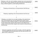
- In a second aspect, embodiments of the present application provide a package method for a wafer level surface acoustic wave filter, including:
- obtaining a wafer, where the wafer includes a substrate layer and a piezoelectric thin film layer, and the substrate layer and the piezoelectric thin film layer are combined together by wafer bonding therebetween;
- preparing an electrode layer on the piezoelectric thin film layer;
- preparing a supporting wall on the piezoelectric thin film layer;
- obtaining a cover plate, where the cover plate includes at least a first material layer, and the first material layer uses the same material as the substrate layer;
- sealing the supporting wall and the cover plate, so that the supporting wall surrounds between the piezoelectric thin film layer and the cover plate to form a sealed cavity.
- In a feasible implementation, a ratio of a thickness of the piezoelectric thin film layer to a thickness of the wafer is less than a preset threshold.
- In a feasible implementation, a value of the preset threshold is 0.1.
- In a feasible implementation, the cover plate includes at least two material layers, and a thickness of each material layer is related to a temperature expansion coefficient of each material layer.
- In a feasible implementation, the cover plate includes the first material layer and a second material layer, the first material layer and the second material layer are combined together by wafer bonding therebetween, and the second material layer uses the same material as the piezoelectric thin film layer.
- In a feasible implementation, the cover plate includes the first material layer, a second material layer and a third material layer; the third material layer is located between the first material layer and the second material layer, and the first material layer and the second material layer are combined together by using the third material layer; and the second material layer uses the same material as the piezoelectric thin film layer.
- In a feasible implementation, the package method further includes:
forming a via hole which penetrates the cover plate and the supporting wall in a through silicon via (TSV) manner at a preset position of the cover plate, and implanting a solder ball in the via hole by electroplating, the solder ball electrically contacting the electrode layer. - Embodiments of the present application provide a wafer level surface acoustic wave filter and a package method, the surface acoustic wave filter includes a wafer, an electrode layer, a supporting wall and a cover plate; where, the wafer includes a substrate layer and a piezoelectric thin film layer combined together by wafer bonding, the electrode layer is arranged on a surface of the piezoelectric thin film layer, the supporting wall is located between the piezoelectric thin film layer and the cover plate, and the supporting wall surrounds between the piezoelectric thin film layer and the cover plate to form a sealed cavity; the cover plate includes at least a first material layer, which uses the same material as the substrate layer. In the embodiments of the present application, through the use of wafer level package, the size of the surface acoustic wave filter can be effectively reduced; the substrate layer and the piezoelectric thin film layer are combined together by wafer bonding, the performance of the surface acoustic wave filter based on this type of wafer is less affected by temperature; and the cover plate uses the same or similar material as the wafer, which can enhance the reliability and temperature stability of a device.
- In order to illustrate technical solutions in the embodiments of the present application or the prior art more clearly, the following will briefly introduce drawings that need to be used in the description of the embodiments of the present application or the prior art. Obviously, the drawings in the following description are some embodiments of the present application, and for those skilled in the art, other drawings can be obtained based on these drawings without creative work.
-
FIG. 1 is a schematic top view of a package structure of a wafer level surface acoustic wave filter in an embodiment of the present application; -
FIG. 2 is a schematic sectional view I of a package structure of a surface acoustic wave filter taken along a section line AB shown inFIG. 1 ; -
FIG. 3 is a schematic sectional view II of a package structure of a surface acoustic wave filter taken along a section line AB shown inFIG. 1 ; -
FIG. 4 is a schematic sectional view III of a package structure of a surface acoustic wave filter taken along a section line AB shown inFIG. 1 ; -
FIG. 5 is a structural schematic view of an electrode layer within a surface acoustic wave filter in an embodiment of the present application; -
FIG. 6 is a schematic sectional view IV of a package structure of a surface acoustic wave filter taken along a section line AB shown inFIG. 1 ; -
FIG. 7 is a transversely sectional view of a wafer level surface acoustic wave filter in an embodiment of the present application; -
FIG. 8 is a schematic flow diagram I of a package method for a wafer level surface acoustic wave filter in an embodiment of the present application; -
FIG. 9 is a schematic flow diagram II of a package method for a wafer level surface acoustic wave filter in an embodiment of the present application; and -
FIG. 10 is a schematic flow diagram III of a package method for a wafer level surface acoustic wave filter in an embodiment of the present application. - In order to make the objective, technical solutions and advantages of the present application more clear, the technical solutions in embodiments of the present application are described clearly and completely in combination with the accompanying drawings in the embodiments of the present application hereinafter. Obviously, the described embodiments are a part of the embodiments of the present application, but not all of the embodiments. Based on the embodiments in the present application, all other embodiments obtained by those skilled in the art without creative work shall fall within the protection scope of the present application.
- The package of existing surface acoustic wave filters is mostly completed by etching substrate material of chips, which is difficult to process, and it is difficult to meet the current requirements for the size and stability of surface acoustic wave filters.
- In order to solve the above problem, an embodiment of the present application provides a wafer level surface acoustic wave filter, the use of wafer level package can effectively reduce the size of the surface acoustic wave filter, which can be suitable for packaging RF front-end module; additionally, the substrate layer and the piezoelectric thin film layer are combined together by wafer bonding, which can improve the temperature stability of the surface acoustic wave filter; and, the cover plate uses the same or similar material as the substrate layer, thereby further enhancing the reliability of the surface acoustic wave filter, and reducing the influence of temperature changes on the surface acoustic wave filter. The present application is described in detail through the following examples.
- Referring to
FIG. 1, FIG. 1 is a schematic top view of a package structure of a wafer level surface acoustic wave filter in an embodiment of the present application. InFIG. 1 , apackage structure 100 of the abovementioned surface acoustic wave filter includes a number ofsolder balls 101. The package structure can be applied to the wafer-level package of the surface acoustic wave filter, so as to achieve the protection of a working surface of the surface acoustic wave filter and the extraction of electrodes. - In this case, after the package structure shown in
FIG. 1 is packaged, a number of surface acoustic wave filter components can be obtained by cutting. - Referring to
FIG. 2, FIG. 2 is a schematic sectional view I of a package structure of a surface acoustic wave filter taken along a section line AB shown inFIG. 1 . In this case, the section shown inFIG. 2 can be considered as a schematic view of a cross-sectional structure of a surface acoustic wave filter. - In
FIG. 2 , the surface acoustic wave filter includes a wafer, an electrode layer, a supportingwall 205 and a cover plate. In this case, the abovementioned wafer includes asubstrate layer 201 and a piezoelectricthin film layer 202, and thesubstrate layer 201 and the piezoelectricthin film layer 202 are combined together by wafer bonding therebetween. Since a thickness of the piezoelectricthin film layer 202 is less than a preset threshold, the temperature expansion coefficient of the wafer after bonding is close to the temperature expansion coefficient of thesubstrate layer 201. - It should be noted that the thickness of each material layer of the surface acoustic wave filter shown in
FIG. 2 is only for exemplary illustration, and does not represent an actual thickness. - In this case, a way of wafer bonding means that two mirror-polished homogenous or heterogeneous wafers are closely combined through chemical and physical action. After the wafers are bonded, atoms at the interface are subjected to external forces to react, so as to form covalent bonds for combining together, so that a bonding interface reaches a specific bonding strength. In the present embodiment, the use of wafer bonding way is conducive to achieving a low temperature drift and improving the power tolerance performance of the surface acoustic wave filter.
- The abovementioned electrode layer includes an
interdigital electrode 203 and a thickenedelectrode 204, and the thickenedelectrode 204 is distributed in at least one of following positions of the interdigital electrode 203: an input position, an output position, and an earthing position. - In this case, the abovementioned
interdigital electrode 203 is arranged on a surface of the piezoelectricthin film layer 202. Optionally, theinterdigital electrode 203 and the thickenedelectrode 204 can be formed on the surface of the piezoelectric thin film layer 102 by photoetching method. - The supporting
wall 205 is located between the piezoelectricthin film layer 202 and the cover plate, and the supportingwall 205 surrounds between the piezoelectricthin film layer 202 and the cover plate to form a sealedcavity 207. - In this case, the cover plate can include only one layer of material, i.e., a
first material layer 206, and thefirst material layer 206 uses the same material as thesubstrate layer 201. - Optionally, the
substrate layer 201 can be made from silicon Si and sapphire, etc., with a thickness of 30λ∼150λ. - Optionally, the piezoelectric
thin film layer 202 can be made from film material with piezoelectric performance, such as lithium tantalate LiTaO3 and lithium niobate LiNbO3, etc., with a thickness of 0.05λ∼15λ. - Exemplarily, the
substrate layer 201 and the piezoelectricthin film layer 202 can be a combination of the following materials:
LiTaO3 and Si, LiNbO3 and Si, LiTaO3 and sapphire, LiNbO3 and sapphire. - Optionally, the electrode layer can be made from aluminum, copper, gold, aluminum-copper alloy, etc., with a thickness of 6%λ∼15%λ, where λ is a wavelength of a surface acoustic wave.
- Optionally, the supporting
wall 205 can be made from viscous materials, which can surround the electrode layer. - In this case, a ratio of a thickness of the piezoelectric thin film layer to that of the wafer is less than a preset threshold. For example, a ratio of the thickness of the piezoelectric thin film layer to that of the wafer is less than 0.1.
- It will be appreciated that, since the LiTaO3 or LiNbO3 used in the piezoelectric
thin film layer 202 has a relatively large temperature expansion coefficient, when the temperature changes, a formed filter device has a relatively large frequency drift. In the embodiment of the present application, by reducing the thickness of the piezoelectric thin film layer and combining with onesubstrate layer 201 with a relatively small temperature expansion coefficient, the frequency drift of the filter device can be effectively reduced. - Exemplarily, the thickness of the piezoelectric
thin film layer 202 can be set below 20 um, and the thickness of thesubstrate layer 201 can be set at about 230 um. - It will be appreciated that, in the embodiment of the present application, the piezoelectric
thin film layer 202 is relatively thin, and has a relatively small contribution to the temperature expansion coefficient of the entire wafer, thus, only a single layer of material same as a substrate material can be used to make the cover plate, so that the temperature expansion coefficient of the cover plate can be close to the temperature expansion coefficient of the wafer. As a result, when the temperature changes, it can prevent deformation of the cover plate and the wafer in different magnitudes due to a large difference between the temperature expansion coefficient of the cover plate and the temperature expansion coefficient of the wafer, which damages the sealedcavity 207. It reduces the influence of temperature changes on the surface acoustic wave filter, thereby effectively enhancing the reliability of the surface acoustic wave filter. - In the embodiment of the present application, the use of wafer level package can effectively reduce the size of the surface acoustic wave filter, which can be suitable for the application in packaging RF front-end module; additionally, the substrate layer and the piezoelectric thin film layer are combined together by wafer bonding, thus the performance of the surface acoustic wave filter based on this type of wafer is less affected by temperature; and the cover plate uses the same material as the substrate layer, thereby also enhancing the overall reliability of the surface acoustic wave filter, and further reducing the influence of temperature changes on the surface acoustic wave filter.
- Based on the contents described in the above embodiment, in another embodiment of the present application, the abovementioned cover plate includes at least two material layers, the thickness of each material layer can be flexibly set according to the temperature expansion coefficient of each material layer, so as to reduce the influence of external temperature changes on the entire surface acoustic wave filter.
- Referring to
FIG. 3, FIG. 3 is a schematic sectional view II of a package structure of a surface acoustic wave filter taken along a section line AB shown inFIG. 1 . In this case, the section shown inFIG. 3 can be considered as a schematic view of a cross-sectional structure of a surface acoustic wave filter. - In
FIG. 3 , the surface acoustic wave filter includes a wafer, an electrode layer, a supportingwall 205 and a cover plate. In this case, the abovementioned wafer includes asubstrate layer 201 and a piezoelectricthin film layer 202, and thesubstrate layer 201 and the piezoelectricthin film layer 202 are combined together by wafer bonding therebetween. - It should be noted that the thickness of each material layer of the surface acoustic wave filter shown in
FIG. 3 is only for exemplary illustration, and does not represent an actual thickness. - The abovementioned electrode layer includes an
interdigital electrode 203 and a thickenedelectrode 204, and the thickenedelectrode 204 is distributed in at least one of following positions of the interdigital electrode 203: an input position, an output position, and an earthing position. In this case, theinterdigital electrode 203 is arranged on a surface of the piezoelectricthin film layer 202. - The supporting
wall 205 is located between the piezoelectricthin film layer 202 and the cover plate, and the supportingwall 205 surrounds between the piezoelectricthin film layer 202 and the cover plate to form a sealedcavity 207. - The abovementioned cover plate includes two layers of materials, i.e., a
first material layer 206 and asecond material layer 301, and thefirst material layer 206 and thesecond material layer 301 are combined together by wafer bonding therebetween. - In this case, the
second material layer 301 is located on a side of the cover plate close to the sealed cavity 208, and thefirst material layer 206 uses the same material as thesubstrate layer 201, and thesecond material layer 301 uses the same material as the piezoelectricthin film layer 202. - It will be appreciated that, in the embodiment of the present application, the material used for the cover plate is the same as the material used for the wafer, that is, the temperature expansion coefficient of the cover plate can be equal to or very close to the temperature expansion coefficient of the wafer. As a result, when the temperature changes, it can prevent the damage to the sealed
cavity 207 due to a large difference between the temperature expansion coefficient of the cover plate and the temperature expansion coefficient of the wafer. It eliminates the influence of temperature changes on such package structure, thereby more effectively enhancing the reliability of the surface acoustic wave filter. - Based on the contents described in the above embodiment, referring to
FIG. 4, FIG. 4 is a schematic sectional view III of a package structure of a surface acoustic wave filter taken along a section line AB shown inFIG. 1 . In this case, the section shown inFIG. 4 can be considered as a schematic view of a cross-sectional structure of a surface acoustic wave filter. - In
FIG. 4 , the surface acoustic wave filter includes a wafer, an electrode layer, a supportingwall 205 and a cover plate. In this case, the abovementioned wafer includes asubstrate layer 201 and a piezoelectricthin film layer 202, and thesubstrate layer 201 and the piezoelectricthin film layer 202 are combined together by wafer bonding therebetween. - It should be noted that the thickness of each material layer of the surface acoustic wave filter shown in
FIG. 4 is only for exemplary illustration, and does not represent an actual thickness. - The abovementioned electrode layer includes an
interdigital electrode 203 and a thickenedelectrode 204, and the thickenedelectrode 204 is distributed in at least one of following positions of the interdigital electrode 203: an input position, an output position, and an earthing position. In this case, theinterdigital electrode 203 is arranged on a surface of the piezoelectricthin film layer 202. - The supporting
wall 205 is located between the piezoelectricthin film layer 202 and the cover plate, and the supportingwall 205 surrounds between the piezoelectricthin film layer 202 and the cover plate to form a sealedcavity 207. - The abovementioned cover plate includes three layers of materials, i.e., a
first material layer 206, asecond material layer 301 and a third material layer 401. In this case, the third material layer 401 is located between thefirst material layer 206 and thesecond material layer 301, and thefirst material layer 206 and thesecond material layer 301 are combined together by using the third material layer 401. - In this case, the
second material layer 301 is located on a side of the cover plate close to the sealed cavity 208; and thefirst material layer 206 uses the same material as thesubstrate layer 201, thesecond material layer 301 uses the same material as the piezoelectricthin film layer 202. - Optionally, a material used for the third material layer 401 is an organic binder.
- In the embodiment of the present application, the thickness of the above three layers of materials can be adjusted and combined flexibly, so as to achieve a temperature expansion coefficient close to that of the bonded wafer. As a result, when the temperature changes, it can also prevent the damage to the sealed
cavity 207 due to a large difference between the temperature expansion coefficient of the cover plate and the temperature expansion coefficient of the wafer. It reduces the influence of temperature changes on such package structure, thereby effectively enhancing the reliability of the surface acoustic wave filter. - Based on the contents described in the above embodiment, referring to
FIG. 5, FIG. 5 is a structural schematic view of an electrode layer within a surface acoustic wave filter in an embodiment of the present application. - In
FIG. 5 , the electrode layer includesinterdigital electrodes 203 and a thickenedelectrode 204, both sides of theinterdigital electrodes 203 includereflection gratings 501, the bus bar of theinterdigital electrodes 203 is abus bar 502, and the bus bar of thereflection gratings 501 is abus bar 503. The thickenedelectrode 204 is distributed on a surface of thebus bar 502. - Since the abovementioned electrode layer has a symmetrical structure, the bus bars of the
interdigital electrodes 203 as ports are reciprocal. - Furthermore, in a feasible implementation of the present application, the
solder ball 101 penetrates the cover plate and the supportingwall 205 in the TSV manner and then electrically contacts the electrode layer. - In another feasible implementation of the present application, the
solder ball 101 is electrically connected with the electrode layer in the RDL manner. - In order to better understand the present application, referring to
FIG. 6, FIG. 6 is a schematic sectional view IV of a package structure of a surface acoustic wave filter taken along a section line AB shown inFIG. 1 . - In
FIG. 6 , assuming that the cover plate only includes one layer of material, i.e., thefirst material layer 206. In this case, when thesolder ball 101 is electrically connected with the electrode layer in the RDL manner, the abovementioned surface acoustic wave filter further includes: a first insulatinglayer 601, ametal wiring layer 602, and a second insulatinglayer 603. - In this case, the first insulating
layer 601 covers a surface of thefirst material layer 206, themetal wiring layer 602 is arranged on the first insulatinglayer 601, and themetal wiring layer 602 is in electrical contact with the abovementioned electrode layer; the second insulatinglayer 603 covers themetal wiring layer 602 and the first insulatinglayer 601, and the second insulatinglayer 603 has at least one opening, where the abovementionedmetal wiring layer 602 can be exposed at each opening, and thesolder balls 101 are filled in each opening and are in electrical contact with the abovementionedmetal wiring layer 602. - It will be appreciated that, in
FIG. 2 to FIG. 4 thesolder balls 101 can be also in electrical contact with the electrode layer in the RDL manner as shown inFIG. 6 . - Furthermore, referring to
FIG. 7, FIG. 7 is a transversely sectional view of a surface acoustic wave filter in an embodiment of the present application. - In
FIG. 7 , 701 represents metal wirings, 702 represents a resonator, 202 represents a piezoelectric thin film layer, 203 represents an interdigital electrode, 204 represents a thickened electrode, 205 represents a supporting wall, and 101 represents a solder ball. Theinterdigital electrode 203 and the thickenedelectrode 204 utilize thesolder balls 101 to achieve the electrical connection with external devices. - It will be appreciated that, the wiring manner shown in
FIG. 7 is only for exemplary illustration, and the purpose is to better understand the embodiments of the present application, and does not represent actual wiring manners such as routing or connection. - Furthermore, based on the contents described in the above embodiment, an embodiment of the present application further provides a package method for a wafer level surface acoustic wave filter. Referring to
FIG. 8, FIG. 8 is a schematic flow diagram I of a package method for a wafer level surface acoustic wave filter in an embodiment of the present application, where the method includes: - S801: obtaining a wafer, where the wafer includes a substrate layer and a piezoelectric thin film layer, and the substrate layer and the piezoelectric thin film layer are combined together by wafer bonding therebetween;
- S802: preparing an electrode layer on the piezoelectric thin film layer;
- S803: preparing a supporting wall on the piezoelectric thin film layer;
- S804: obtaining a cover plate, where the cover plate includes a first material layer, and the first material layer uses the same material as the substrate layer;
- S805: sealing the supporting wall and the cover plate, so that the supporting wall surrounds between the piezoelectric thin film layer and the cover plate to form a sealed cavity.
- In this case, a via hole which penetrates the cover plate and the supporting wall is formed in a through silicon via (TSV) manner at a preset position of the cover plate; and a solder ball is implanted in the via hole by electroplating, the solder ball electrically contacts the electrode layer.
- In a feasible implementation, a ratio of a thickness of the piezoelectric thin film layer to that of the wafer is less than a preset threshold. Optionally, a value of the preset threshold is 0.1.
- It will be appreciated that, in the embodiment of the present application, the piezoelectric
thin film layer 202 is relatively thin, and has a relatively small contribution to the temperature expansion coefficient of the entire wafer, thus, only a single layer of material same as a substrate material can be used to make the cover plate, so that the temperature expansion coefficient of the cover plate can be close to the temperature expansion coefficient of the wafer. As a result, when the temperature changes, it can prevent deformation of the cover plate and the wafer in different magnitudes due to a large difference between the temperature expansion coefficient of the cover plate and the temperature expansion coefficient of the wafer, which damages the sealedcavity 207. It reduces the influence of temperature changes on the surface acoustic wave filter, thereby effectively enhancing the reliability of the surface acoustic wave filter. - The package method for a wafer level surface acoustic wave filter provided by the embodiment of the present application uses wafer level package, which can effectively reduce the size of the surface acoustic wave filter; additionally, since the substrate layer and the piezoelectric thin film layer are combined together by wafer bonding, the performance of the surface acoustic wave filter based on this type of wafer is less affected by temperature; meanwhile, the cover plate uses the same material as the substrate material, so that the temperature expansion coefficient of the cover plate can be the same as the temperature expansion coefficient of the wafer. As a result, when the temperature changes, it can prevent the damage to the sealed cavity due to a large difference between the temperature expansion coefficient of the cover plate and the temperature expansion coefficient of the wafer. It reduces the influence of temperature changes on the surface acoustic wave filter, thereby effectively enhancing the reliability of the surface acoustic wave filter.
- Based on the contents described in the above embodiment, in another embodiment of the present application, the abovementioned cover plate includes at least two material layers, and a thickness of each material layer is related to a temperature expansion coefficient of each material layer.
- Referring to
FIG. 9, FIG. 9 is a schematic flow diagram II of a package method for a wafer level surface acoustic wave filter in an embodiment of the present application, where the method includes: - S901: obtaining a wafer, where the wafer includes a substrate layer and a piezoelectric thin film layer, and the substrate layer and the piezoelectric thin film layer are combined together by wafer bonding therebetween;
- S902: preparing an electrode layer on the piezoelectric thin film layer;
- S903: preparing a supporting wall on the piezoelectric thin film layer;
- S904: obtaining a cover plate, where the cover plate includes a first material layer and a second material layer, the first material layer and the second material layer are combined together by wafer bonding therebetween, the first material layer uses the same material as the substrate layer, and the second material layer uses the same material as the piezoelectric thin film layer;
- S905: sealing the supporting wall and the cover plate, so that the supporting wall surrounds between the piezoelectric thin film layer and the cover plate to form a sealed cavity.
- In the package method for a wafer level surface acoustic wave filter provided by the embodiment of the present application, the material used for the cover plate is the same as the material used for the wafer, that is, the temperature expansion coefficient of the cover plate can be equal to or very close to the temperature expansion coefficient of the wafer. As a result, when the temperature changes, it can prevent the damage to the sealed cavity due to a large difference between the temperature expansion coefficient of the cover plate and the temperature expansion coefficient of the wafer. It eliminates the influence of temperature changes on such package structure, thereby more effectively enhancing the temperature stability of the surface acoustic wave filter.
- Based on the contents described in the above embodiment, in yet another embodiment of the present application, referring to
FIG. 10, FIG. 10 is a schematic flow diagram III of a package method for a wafer level surface acoustic wave filter in an embodiment of the present application, where the method includes: - S1001: obtaining a wafer, where the wafer includes a substrate layer and a piezoelectric thin film layer, and the substrate layer and the piezoelectric thin film layer are combined together by wafer bonding therebetween;
- S1002: preparing an electrode layer on the piezoelectric thin film layer;
- S1003: preparing a supporting wall on the piezoelectric thin film layer;
- S1004: obtaining a cover plate, where the cover plate includes a first material layer, a second material layer and a third material layer; the first material layer and the second material layer are combined together by using the third material layer; the first material layer uses the same material as the substrate layer, and the second material layer uses the same material as the piezoelectric thin film layer;
- S1005: sealing the supporting wall and the cover plate, so that the supporting wall surrounds between the piezoelectric thin film layer and the cover plate to form a sealed cavity.
- In the package method for a wafer level surface acoustic wave filter provided by the embodiment of the present application, the thickness of the above three layers of materials can be adjusted and combined flexibly, so as to achieve a temperature expansion coefficient close to that of the bonded wafer. As a result, when the temperature changes, it can also prevent the damage to the sealed cavity due to a large difference between the temperature expansion coefficient of the cover plate and the temperature expansion coefficient of the wafer. It reduces the influence of temperature changes on such package structure, thereby effectively enhancing the temperature stability of the surface acoustic wave filter.
- The above embodiments are only used to illustrate the technical solutions of the present application, but not to limit them. Although the present application has been described in detail with reference to the above embodiments, those skilled in the art should understand that they can still make modifications to the technical solutions recorded in the above embodiments, or equivalent substitutions to some or all of the technical features therein, and these modifications or substitutions do not make the essential of the corresponding technical solutions depart from the scope of the technical solutions in the embodiments according to the present application.
Claims (18)
- A wafer level surface acoustic wave filter, comprising: a wafer, an electrode layer, a supporting wall and a cover plate; wherein the wafer comprises a substrate layer and a piezoelectric thin film layer, and the substrate layer and the piezoelectric thin film layer are combined together by wafer bonding therebetween;the electrode layer is arranged on a surface of the piezoelectric thin film layer, the supporting wall is located between the piezoelectric thin film layer and the cover plate, and the supporting wall surrounds between the piezoelectric thin film layer and the cover plate to form a sealed cavity;the cover plate comprises at least a first material layer, and the first material layer uses the same material as the substrate layer.
- The wafer level surface acoustic wave filter according to claim 1, wherein a ratio of a thickness of the piezoelectric thin film layer to a thickness of the wafer is less than a preset threshold.
- The wafer level surface acoustic wave filter according to claim 2, wherein a value of the preset threshold is 0.1.
- The wafer level surface acoustic wave filter according to claim 1, wherein the cover plate comprises at least two material layers, and a thickness of each material layer is related to a temperature expansion coefficient of each material layer.
- The wafer level surface acoustic wave filter according to claim 4, wherein the cover plate comprises the first material layer and a second material layer, the first material layer and the second material layer are combined together by wafer bonding therebetween;the second material layer is located on a side of the cover plate close to the sealed cavity; andthe second material layer uses the same material as the piezoelectric thin film layer.
- The wafer level surface acoustic wave filter according to claim 4, wherein the cover plate comprises the first material layer, a second material layer and a third material layer; the third material layer is located between the first material layer and the second material layer, and the first material layer and the second material layer are combined together by using the third material layer;the second material layer is located on a side of the cover plate close to the sealed cavity; andthe second material layer uses the same material as the piezoelectric thin film layer.
- The wafer level surface acoustic wave filter according to claim 6, wherein a material used for the third material layer is an organic binder.
- The wafer level surface acoustic wave filter according to claim 1, wherein the electrode layer comprises an interdigital electrode and a thickened electrode, and the thickened electrode is distributed in at least one of following positions of the interdigital electrode: an input position, an output position, and an earthing position.
- The wafer level surface acoustic wave filter according to claim 8, further comprising at least one solder ball, the solder ball penetrates the cover plate and the supporting wall in a through silicon via (TSV) manner and then electrically contacts the electrode layer;
or, the solder ball is electrically connected with the electrode layer in a redistribution layer (RDL) manner. - The wafer level surface acoustic wave filter according to any one of claims 1-9, wherein the piezoelectric thin film layer is made from at least one of following materials: lithium tantalate LiTaO3 and lithium niobate LiNbO3.
- The wafer level surface acoustic wave filter according to any one of claims 1-9, wherein the substrate layer is made from at least one of following materials: silicon Si and sapphire.
- A package method for a wafer level surface acoustic wave filter, comprising:obtaining a wafer, the wafer comprising a substrate layer and a piezoelectric thin film layer, and the substrate layer and the piezoelectric thin film layer being combined together by wafer bonding therebetween;preparing an electrode layer on the piezoelectric thin film layer;preparing a supporting wall on the piezoelectric thin film layer;obtaining a cover plate, the cover plate comprising at least a first material layer, the first material layer using the same material as the substrate layer; andsealing the supporting wall and the cover plate, so that the supporting wall surrounds between the piezoelectric thin film layer and the cover plate to form a sealed cavity.
- The package method according to claim 12, wherein a ratio of a thickness of the piezoelectric thin film layer to a thickness of the wafer is less than a preset threshold.
- The package method according to claim 13, wherein a value of the preset threshold is 0.1.
- The package method according to claim 12, wherein the cover plate comprises at least two material layers, and a thickness of each material layer is related to a temperature expansion coefficient of each material layer.
- The package method according to claim 15, wherein the cover plate comprises the first material layer and a second material layer, the first material layer and the second material layer are combined together by wafer bonding therebetween, and the second material layer uses the same material as the piezoelectric thin film layer.
- The package method according to claim 15, wherein the cover plate comprises the first material layer, a second material layer and a third material layer; the third material layer is located between the first material layer and the second material layer, and the first material layer and the second material layer are combined together by using the third material layer; and the second material layer uses the same material as the piezoelectric thin film layer.
- The package method according to claim 12, further comprising:
forming a via hole which penetrates the cover plate and the supporting wall in a through silicon via (TSV) manner at a preset position of the cover plate, and implanting a solder ball in the via hole by electroplating, the solder ball electrically contacting the electrode layer.
Applications Claiming Priority (2)
| Application Number | Priority Date | Filing Date | Title |
|---|---|---|---|
| CN202010787875.6A CN111786647B (en) | 2020-08-07 | 2020-08-07 | Wafer-level surface acoustic wave filter and packaging method |
| PCT/CN2021/098266 WO2022028080A1 (en) | 2020-08-07 | 2021-06-04 | Wafer-level surface acoustic wave filter and packaging method |
Publications (2)
| Publication Number | Publication Date |
|---|---|
| EP3972130A1 true EP3972130A1 (en) | 2022-03-23 |
| EP3972130A4 EP3972130A4 (en) | 2022-09-07 |
Family
ID=72766008
Family Applications (1)
| Application Number | Title | Priority Date | Filing Date |
|---|---|---|---|
| EP21802176.4A Withdrawn EP3972130A4 (en) | 2020-08-07 | 2021-06-04 | PADDLE LEVEL SURFACE ACOUSTIC WAVE FILTER AND CONDITIONING METHOD |
Country Status (7)
| Country | Link |
|---|---|
| US (1) | US11632095B2 (en) |
| EP (1) | EP3972130A4 (en) |
| JP (1) | JP7449315B2 (en) |
| KR (1) | KR102843095B1 (en) |
| CN (1) | CN111786647B (en) |
| TW (1) | TWI797704B (en) |
| WO (1) | WO2022028080A1 (en) |
Families Citing this family (21)
| Publication number | Priority date | Publication date | Assignee | Title |
|---|---|---|---|---|
| CN111786647B (en) * | 2020-08-07 | 2021-06-15 | 展讯通信(上海)有限公司 | Wafer-level surface acoustic wave filter and packaging method |
| CN112697262B (en) * | 2020-12-08 | 2023-06-27 | 联合微电子中心有限责任公司 | Hydrophone and method for manufacturing same |
| CN113054942A (en) * | 2021-03-11 | 2021-06-29 | 展讯通信(上海)有限公司 | Surface acoustic wave filter and packaging method |
| CN113436999A (en) * | 2021-07-06 | 2021-09-24 | 电子科技大学 | Wafer temperature field measuring device based on surface acoustic wave sensing technology |
| CN113783546A (en) * | 2021-07-09 | 2021-12-10 | 无锡市好达电子股份有限公司 | A chip-level packaged sound meter device and its preparation method |
| CN113539986A (en) * | 2021-07-19 | 2021-10-22 | 天通瑞宏科技有限公司 | A wafer level packaging structure |
| CN115276595A (en) * | 2022-07-04 | 2022-11-01 | 深圳市汇芯通信技术有限公司 | Surface acoustic wave filter, surface acoustic wave resonator, and method of manufacturing the same |
| CN115051667B (en) * | 2022-08-12 | 2022-11-01 | 深圳新声半导体有限公司 | Method for wafer-level packaging of surface acoustic wave filter and surface acoustic wave filter |
| US12587155B2 (en) * | 2022-09-16 | 2026-03-24 | Shenzhen Newsonic Technology Co., Ltd. | Manufacturing method of surface acoustic wave filter with back electrode of piezoelectric layer |
| US12074586B2 (en) * | 2022-09-16 | 2024-08-27 | Shenzhen Newsonic Technologies Co., Ltd. | Structure and manufacturing method of surface acoustic wave filter with back electrode of piezoelectric layer |
| CN115567025A (en) * | 2022-10-20 | 2023-01-03 | 中北大学 | Multilayer structure spurious response free SH type surface acoustic wave filter |
| CN115833785A (en) * | 2022-12-16 | 2023-03-21 | 深圳飞骧科技股份有限公司 | Wafer-level surface acoustic wave filter and radio frequency module chip |
| CN115987245B (en) * | 2022-12-16 | 2026-04-28 | 深圳飞骧科技股份有限公司 | Wafer-level surface acoustic wave filter and RF module chip |
| CN116232263B (en) * | 2023-02-10 | 2025-07-29 | 深圳飞骧科技股份有限公司 | Packaging method, packaging structure and radio frequency module of duplexer wafer level |
| CN116155229B (en) * | 2023-02-17 | 2023-11-28 | 北京超材信息科技有限公司 | Surface acoustic wave device and method of manufacturing the same |
| US20240371711A1 (en) * | 2023-05-05 | 2024-11-07 | Advanced Semiconductor Engineering, Inc. | Package structure |
| CN117728791B (en) * | 2023-06-30 | 2025-02-18 | 荣耀终端有限公司 | Filter, filter manufacturing process and electronic equipment |
| CN117833847A (en) * | 2024-01-05 | 2024-04-05 | 唯捷创芯(天津)电子技术股份有限公司 | Filter and packaging method thereof |
| CN117713741B (en) * | 2024-02-04 | 2024-06-25 | 深圳新声半导体有限公司 | Film surface acoustic wave filter and manufacturing method thereof |
| CN120729216A (en) * | 2024-03-27 | 2025-09-30 | 华为技术有限公司 | Wafer-level packaging structure, manufacturing method thereof, radio frequency component and electronic equipment |
| CN118740096B (en) * | 2024-07-18 | 2025-02-11 | 深圳新声半导体有限公司 | A surface acoustic wave wafer-level structure and manufacturing method thereof, and electronic equipment |
Family Cites Families (40)
| Publication number | Priority date | Publication date | Assignee | Title |
|---|---|---|---|---|
| US7230512B1 (en) * | 2003-08-19 | 2007-06-12 | Triquint, Inc. | Wafer-level surface acoustic wave filter package with temperature-compensating characteristics |
| JP2006197554A (en) * | 2004-12-17 | 2006-07-27 | Seiko Epson Corp | Surface acoustic wave device and manufacturing method thereof, IC card, portable electronic device |
| DE102005026243B4 (en) * | 2005-06-07 | 2018-04-05 | Snaptrack, Inc. | Electrical component and manufacturing method |
| JP4760222B2 (en) * | 2005-08-26 | 2011-08-31 | セイコーエプソン株式会社 | Surface acoustic wave device |
| JP4289399B2 (en) * | 2006-06-22 | 2009-07-01 | セイコーエプソン株式会社 | Acoustic wave device and method of manufacturing acoustic wave device |
| US8476809B2 (en) * | 2008-04-29 | 2013-07-02 | Sand 9, Inc. | Microelectromechanical systems (MEMS) resonators and related apparatus and methods |
| WO2010114602A1 (en) * | 2009-03-31 | 2010-10-07 | Sand9, Inc. | Integration of piezoelectric materials with substrates |
| US9048811B2 (en) * | 2009-03-31 | 2015-06-02 | Sand 9, Inc. | Integration of piezoelectric materials with substrates |
| JP5056837B2 (en) * | 2009-12-21 | 2012-10-24 | 株式会社村田製作所 | Method for manufacturing piezoelectric device |
| US8836449B2 (en) * | 2010-08-27 | 2014-09-16 | Wei Pang | Vertically integrated module in a wafer level package |
| CN202103092U (en) * | 2010-11-29 | 2012-01-04 | 上海蓝宝光电材料有限公司 | Efficient and high voltage bond-type LED chip structure with electrodes on side walls |
| JP5999833B2 (en) * | 2011-06-08 | 2016-09-28 | 日本電波工業株式会社 | Crystal device |
| WO2014034326A1 (en) * | 2012-08-29 | 2014-03-06 | 株式会社村田製作所 | Elastic wave apparatus |
| CN103117724B (en) * | 2013-01-09 | 2016-12-28 | 宁波大学 | Piezoelectric resonator |
| JP6385648B2 (en) * | 2013-05-14 | 2018-09-05 | 太陽誘電株式会社 | Acoustic wave device and method of manufacturing acoustic wave device |
| JP6464735B2 (en) * | 2014-12-25 | 2019-02-06 | 株式会社村田製作所 | Elastic wave device and manufacturing method thereof |
| JP6397352B2 (en) * | 2015-02-19 | 2018-09-26 | 太陽誘電株式会社 | Elastic wave device |
| US10574203B2 (en) * | 2015-07-28 | 2020-02-25 | Qorvo Us, Inc. | Bonded wafers and surface acoustic wave devices using same |
| JP2017135230A (en) * | 2016-01-27 | 2017-08-03 | ルネサスエレクトロニクス株式会社 | Semiconductor device and manufacturing method of the same |
| JP6509147B2 (en) * | 2016-02-29 | 2019-05-08 | 太陽誘電株式会社 | Electronic device |
| CN106301283A (en) * | 2016-11-07 | 2017-01-04 | 无锡吉迈微电子有限公司 | The encapsulating structure of SAW filter and manufacture method |
| CN206195735U (en) | 2016-11-07 | 2017-05-24 | 无锡吉迈微电子有限公司 | Encapsulation structure of sound surface wave filter |
| US10439587B2 (en) * | 2016-12-02 | 2019-10-08 | Skyworks Solutions, Inc. | Methods of manufacturing electronic devices formed in a cavity |
| JP6696917B2 (en) * | 2017-01-18 | 2020-05-20 | 信越化学工業株式会社 | Manufacturing method of composite substrate |
| US11031919B2 (en) * | 2017-03-31 | 2021-06-08 | Kyocera Corporation | Elastic wave device, duplexer, and communication device |
| CN110771035B (en) * | 2017-06-21 | 2023-08-08 | 株式会社村田制作所 | Elastic wave device |
| CN107493086B (en) * | 2017-09-04 | 2023-08-15 | 杭州左蓝微电子技术有限公司 | Temperature-compensated surface acoustic wave resonator and preparation method thereof |
| CN107919862B (en) * | 2017-12-28 | 2024-08-06 | 中电科芯片技术(集团)有限公司 | Surface acoustic wave device airtight wafer-level packaging structure and process |
| CN108233890A (en) * | 2018-01-09 | 2018-06-29 | 华天科技(昆山)电子有限公司 | FBAR filter packages structure and packaging method |
| US20190221607A1 (en) | 2018-01-14 | 2019-07-18 | Innovative Micro Technology | Microfabricated device with piezoelectric substrate and method of manufacture |
| US10630259B2 (en) * | 2018-02-05 | 2020-04-21 | Zhuhai Crystal Resonance Technologies Co., Ltd. | Single crystal piezoelectric RF resonators and filters with improved cavity definition |
| CN108155287A (en) * | 2018-02-11 | 2018-06-12 | 海宁市瑞宏科技有限公司 | A kind of wafer scale SAWF encapsulating structures with resisting temperature impact effect |
| TWI677951B (en) | 2018-11-09 | 2019-11-21 | 恆勁科技股份有限公司 | Surface acoustic wave filter packaging structure and manufacturing method thereof |
| CN111326482A (en) | 2018-12-13 | 2020-06-23 | 中芯集成电路(宁波)有限公司 | Packaging structure of surface acoustic wave device and wafer-level packaging method thereof |
| CN110247639B (en) * | 2019-07-01 | 2024-05-07 | 中电科技德清华莹电子有限公司 | Radio frequency surface acoustic wave filter chip and manufacturing process |
| CN110995189A (en) * | 2019-10-28 | 2020-04-10 | 武汉大学 | Lattice structure filter and preparation method thereof |
| CN110993570B (en) * | 2019-12-20 | 2024-09-13 | 苏州科阳光电科技有限公司 | Wafer-level packaging structure and packaging method |
| CN111147040A (en) * | 2019-12-23 | 2020-05-12 | 河源市众拓光电科技有限公司 | A kind of air gap type thin film bulk acoustic wave resonator and preparation method thereof |
| CN111313861B (en) * | 2020-02-25 | 2024-03-08 | 绍兴中芯集成电路制造股份有限公司 | Surface acoustic wave resonator and method of forming the same |
| CN111786647B (en) * | 2020-08-07 | 2021-06-15 | 展讯通信(上海)有限公司 | Wafer-level surface acoustic wave filter and packaging method |
-
2020
- 2020-08-07 CN CN202010787875.6A patent/CN111786647B/en active Active
-
2021
- 2021-06-04 WO PCT/CN2021/098266 patent/WO2022028080A1/en not_active Ceased
- 2021-06-04 JP JP2021571562A patent/JP7449315B2/en active Active
- 2021-06-04 EP EP21802176.4A patent/EP3972130A4/en not_active Withdrawn
- 2021-06-04 KR KR1020217039300A patent/KR102843095B1/en active Active
- 2021-08-05 TW TW110128907A patent/TWI797704B/en active
- 2021-12-07 US US17/544,124 patent/US11632095B2/en active Active
Also Published As
| Publication number | Publication date |
|---|---|
| CN111786647A (en) | 2020-10-16 |
| TWI797704B (en) | 2023-04-01 |
| KR102843095B1 (en) | 2025-08-05 |
| JP7449315B2 (en) | 2024-03-13 |
| JP2022546753A (en) | 2022-11-08 |
| US11632095B2 (en) | 2023-04-18 |
| TW202220380A (en) | 2022-05-16 |
| US20220094328A1 (en) | 2022-03-24 |
| CN111786647B (en) | 2021-06-15 |
| KR20220019098A (en) | 2022-02-15 |
| EP3972130A4 (en) | 2022-09-07 |
| WO2022028080A1 (en) | 2022-02-10 |
Similar Documents
| Publication | Publication Date | Title |
|---|---|---|
| US11632095B2 (en) | Wafer level surface acoustic wave filter and package method | |
| JP5861771B2 (en) | Elastic wave device and manufacturing method thereof | |
| WO2022188272A1 (en) | Surface acoustic wave filter and packaging method | |
| JP5154516B2 (en) | Solar cell module and method for manufacturing solar cell module | |
| CN111052606B (en) | Elastic wave device and elastic wave module including the elastic wave device | |
| KR20150068495A (en) | Wafer level packaging using flip chip mounting | |
| KR20040110979A (en) | Surface acoustic wave device and method of producing the same | |
| US20230134889A1 (en) | Stacked die transversely-excited film bulk acoustic resonator (xbar) filters | |
| JP2004274574A (en) | Surface acoustic wave device and method of manufacturing the same | |
| KR20200000058A (en) | Surface acoustic wave device package and method of manufacturing the same | |
| CN110098130A (en) | A kind of system-in-a-package method and packaging | |
| US12562716B2 (en) | Single substrate multiplexer | |
| WO2021135013A1 (en) | Semiconductor structure having stacked units and manufacturing method therefor, and electronic device | |
| CN114792751B (en) | Vibration device and method for manufacturing vibration device | |
| JPH1032223A (en) | Semiconductor device | |
| US6495398B1 (en) | Wafer-scale package for surface acoustic wave circuit and method of manufacturing the same | |
| WO2020249467A1 (en) | Electric component, electric device and method for manufacturing a plurality of electric components | |
| US6639150B1 (en) | Hermetic package for surface acoustic wave device having exposed device substrate contacts and method of manufacturing the same | |
| CN110800101A (en) | electronics module | |
| KR20050061372A (en) | Semiconductor device, method for manufacturing the same, circuit board and electronic apparatus | |
| CN109802031B (en) | Packaging method and structure of surface acoustic wave device | |
| CN116260420A (en) | Resonator, forming method thereof, filter and electronic equipment | |
| JP2022500952A (en) | Packaging structure of air gap type semiconductor device and its manufacturing method | |
| JP2012186633A (en) | Electronic component and manufacturing method thereof | |
| CN121461926A (en) | Filter, method for forming the same, and electronic device |
Legal Events
| Date | Code | Title | Description |
|---|---|---|---|
| STAA | Information on the status of an ep patent application or granted ep patent |
Free format text: STATUS: UNKNOWN |
|
| STAA | Information on the status of an ep patent application or granted ep patent |
Free format text: STATUS: THE INTERNATIONAL PUBLICATION HAS BEEN MADE |
|
| PUAI | Public reference made under article 153(3) epc to a published international application that has entered the european phase |
Free format text: ORIGINAL CODE: 0009012 |
|
| STAA | Information on the status of an ep patent application or granted ep patent |
Free format text: STATUS: REQUEST FOR EXAMINATION WAS MADE |
|
| 17P | Request for examination filed |
Effective date: 20211125 |
|
| AK | Designated contracting states |
Kind code of ref document: A1 Designated state(s): AL AT BE BG CH CY CZ DE DK EE ES FI FR GB GR HR HU IE IS IT LI LT LU LV MC MK MT NL NO PL PT RO RS SE SI SK SM TR |
|
| A4 | Supplementary search report drawn up and despatched |
Effective date: 20220805 |
|
| RIC1 | Information provided on ipc code assigned before grant |
Ipc: H03H 3/08 20060101ALI20220801BHEP Ipc: H03H 9/02 20060101ALI20220801BHEP Ipc: H03H 9/10 20060101AFI20220801BHEP |
|
| DAV | Request for validation of the european patent (deleted) | ||
| DAX | Request for extension of the european patent (deleted) | ||
| STAA | Information on the status of an ep patent application or granted ep patent |
Free format text: STATUS: THE APPLICATION HAS BEEN WITHDRAWN |
|
| 18W | Application withdrawn |
Effective date: 20250617 |