EP3971994A1 - Photovoltaic module, backsheet of photovoltaic module, and method for manufacturing photovoltaic module - Google Patents
Photovoltaic module, backsheet of photovoltaic module, and method for manufacturing photovoltaic module Download PDFInfo
- Publication number
- EP3971994A1 EP3971994A1 EP20931723.9A EP20931723A EP3971994A1 EP 3971994 A1 EP3971994 A1 EP 3971994A1 EP 20931723 A EP20931723 A EP 20931723A EP 3971994 A1 EP3971994 A1 EP 3971994A1
- Authority
- EP
- European Patent Office
- Prior art keywords
- thermally conductive
- layer
- conductive layer
- back sheet
- photovoltaic module
- Prior art date
- Legal status (The legal status is an assumption and is not a legal conclusion. Google has not performed a legal analysis and makes no representation as to the accuracy of the status listed.)
- Granted
Links
- 238000004519 manufacturing process Methods 0.000 title claims abstract description 70
- 238000000034 method Methods 0.000 title claims description 11
- 239000010410 layer Substances 0.000 claims description 727
- 239000002245 particle Substances 0.000 claims description 50
- 238000010030 laminating Methods 0.000 claims description 36
- 230000004888 barrier function Effects 0.000 claims description 33
- 230000007704 transition Effects 0.000 claims description 33
- YCKRFDGAMUMZLT-UHFFFAOYSA-N Fluorine atom Chemical compound [F] YCKRFDGAMUMZLT-UHFFFAOYSA-N 0.000 claims description 24
- 239000011737 fluorine Substances 0.000 claims description 24
- 229910052731 fluorine Inorganic materials 0.000 claims description 24
- 238000000576 coating method Methods 0.000 claims description 18
- 229910052782 aluminium Inorganic materials 0.000 claims description 17
- XAGFODPZIPBFFR-UHFFFAOYSA-N aluminium Chemical group [Al] XAGFODPZIPBFFR-UHFFFAOYSA-N 0.000 claims description 17
- 239000011248 coating agent Substances 0.000 claims description 17
- 239000001023 inorganic pigment Substances 0.000 claims description 16
- 239000002952 polymeric resin Substances 0.000 claims description 13
- 229920003002 synthetic resin Polymers 0.000 claims description 13
- RYGMFSIKBFXOCR-UHFFFAOYSA-N Copper Chemical compound [Cu] RYGMFSIKBFXOCR-UHFFFAOYSA-N 0.000 claims description 9
- 239000004020 conductor Substances 0.000 claims description 8
- 238000001035 drying Methods 0.000 claims description 8
- 239000011888 foil Substances 0.000 claims description 8
- 239000011521 glass Substances 0.000 claims description 7
- VTYYLEPIZMXCLO-UHFFFAOYSA-L Calcium carbonate Chemical compound [Ca+2].[O-]C([O-])=O VTYYLEPIZMXCLO-UHFFFAOYSA-L 0.000 claims description 6
- UQSXHKLRYXJYBZ-UHFFFAOYSA-N Iron oxide Chemical compound [Fe]=O UQSXHKLRYXJYBZ-UHFFFAOYSA-N 0.000 claims description 6
- PXHVJJICTQNCMI-UHFFFAOYSA-N Nickel Chemical compound [Ni] PXHVJJICTQNCMI-UHFFFAOYSA-N 0.000 claims description 6
- VYPSYNLAJGMNEJ-UHFFFAOYSA-N Silicium dioxide Chemical compound O=[Si]=O VYPSYNLAJGMNEJ-UHFFFAOYSA-N 0.000 claims description 6
- GWEVSGVZZGPLCZ-UHFFFAOYSA-N Titan oxide Chemical compound O=[Ti]=O GWEVSGVZZGPLCZ-UHFFFAOYSA-N 0.000 claims description 6
- XLOMVQKBTHCTTD-UHFFFAOYSA-N Zinc monoxide Chemical compound [Zn]=O XLOMVQKBTHCTTD-UHFFFAOYSA-N 0.000 claims description 6
- ADCOVFLJGNWWNZ-UHFFFAOYSA-N antimony trioxide Chemical compound O=[Sb]O[Sb]=O ADCOVFLJGNWWNZ-UHFFFAOYSA-N 0.000 claims description 6
- TZCXTZWJZNENPQ-UHFFFAOYSA-L barium sulfate Chemical compound [Ba+2].[O-]S([O-])(=O)=O TZCXTZWJZNENPQ-UHFFFAOYSA-L 0.000 claims description 6
- OSGAYBCDTDRGGQ-UHFFFAOYSA-L calcium sulfate Chemical compound [Ca+2].[O-]S([O-])(=O)=O OSGAYBCDTDRGGQ-UHFFFAOYSA-L 0.000 claims description 6
- 238000004891 communication Methods 0.000 claims description 6
- 229910052802 copper Inorganic materials 0.000 claims description 6
- 239000010949 copper Substances 0.000 claims description 6
- 239000000463 material Substances 0.000 claims description 6
- 239000011241 protective layer Substances 0.000 claims description 6
- 238000005507 spraying Methods 0.000 claims description 6
- BQCADISMDOOEFD-UHFFFAOYSA-N Silver Chemical compound [Ag] BQCADISMDOOEFD-UHFFFAOYSA-N 0.000 claims description 5
- PCHJSUWPFVWCPO-UHFFFAOYSA-N gold Chemical compound [Au] PCHJSUWPFVWCPO-UHFFFAOYSA-N 0.000 claims description 5
- 229910052737 gold Inorganic materials 0.000 claims description 5
- 239000010931 gold Substances 0.000 claims description 5
- 238000007650 screen-printing Methods 0.000 claims description 5
- 229910052709 silver Inorganic materials 0.000 claims description 5
- 239000004332 silver Substances 0.000 claims description 5
- 229920000178 Acrylic resin Polymers 0.000 claims description 4
- 239000004925 Acrylic resin Substances 0.000 claims description 4
- 229910052580 B4C Inorganic materials 0.000 claims description 4
- 229920003180 amino resin Polymers 0.000 claims description 4
- 238000000889 atomisation Methods 0.000 claims description 4
- INAHAJYZKVIDIZ-UHFFFAOYSA-N boron carbide Chemical compound B12B3B4C32B41 INAHAJYZKVIDIZ-UHFFFAOYSA-N 0.000 claims description 4
- PMHQVHHXPFUNSP-UHFFFAOYSA-M copper(1+);methylsulfanylmethane;bromide Chemical compound Br[Cu].CSC PMHQVHHXPFUNSP-UHFFFAOYSA-M 0.000 claims description 4
- 239000003822 epoxy resin Substances 0.000 claims description 4
- 229920000647 polyepoxide Polymers 0.000 claims description 4
- 229910010271 silicon carbide Inorganic materials 0.000 claims description 4
- HBMJWWWQQXIZIP-UHFFFAOYSA-N silicon carbide Chemical compound [Si+]#[C-] HBMJWWWQQXIZIP-UHFFFAOYSA-N 0.000 claims description 4
- 238000004528 spin coating Methods 0.000 claims description 4
- ATJFFYVFTNAWJD-UHFFFAOYSA-N Tin Chemical compound [Sn] ATJFFYVFTNAWJD-UHFFFAOYSA-N 0.000 claims description 3
- MCMNRKCIXSYSNV-UHFFFAOYSA-N ZrO2 Inorganic materials O=[Zr]=O MCMNRKCIXSYSNV-UHFFFAOYSA-N 0.000 claims description 3
- 229920013822 aminosilicone Polymers 0.000 claims description 3
- 229910000019 calcium carbonate Inorganic materials 0.000 claims description 3
- 239000011889 copper foil Substances 0.000 claims description 3
- FPAFDBFIGPHWGO-UHFFFAOYSA-N dioxosilane;oxomagnesium;hydrate Chemical compound O.[Mg]=O.[Mg]=O.[Mg]=O.O=[Si]=O.O=[Si]=O.O=[Si]=O.O=[Si]=O FPAFDBFIGPHWGO-UHFFFAOYSA-N 0.000 claims description 3
- 238000001125 extrusion Methods 0.000 claims description 3
- ZLNQQNXFFQJAID-UHFFFAOYSA-L magnesium carbonate Chemical compound [Mg+2].[O-]C([O-])=O ZLNQQNXFFQJAID-UHFFFAOYSA-L 0.000 claims description 3
- 239000001095 magnesium carbonate Substances 0.000 claims description 3
- 229910000021 magnesium carbonate Inorganic materials 0.000 claims description 3
- 239000000395 magnesium oxide Substances 0.000 claims description 3
- CPLXHLVBOLITMK-UHFFFAOYSA-N magnesium oxide Inorganic materials [Mg]=O CPLXHLVBOLITMK-UHFFFAOYSA-N 0.000 claims description 3
- AXZKOIWUVFPNLO-UHFFFAOYSA-N magnesium;oxygen(2-) Chemical compound [O-2].[Mg+2] AXZKOIWUVFPNLO-UHFFFAOYSA-N 0.000 claims description 3
- 239000010445 mica Substances 0.000 claims description 3
- 229910052618 mica group Inorganic materials 0.000 claims description 3
- 229910052759 nickel Inorganic materials 0.000 claims description 3
- TWNQGVIAIRXVLR-UHFFFAOYSA-N oxo(oxoalumanyloxy)alumane Chemical compound O=[Al]O[Al]=O TWNQGVIAIRXVLR-UHFFFAOYSA-N 0.000 claims description 3
- RVTZCBVAJQQJTK-UHFFFAOYSA-N oxygen(2-);zirconium(4+) Chemical compound [O-2].[O-2].[Zr+4] RVTZCBVAJQQJTK-UHFFFAOYSA-N 0.000 claims description 3
- 239000000377 silicon dioxide Substances 0.000 claims description 3
- 235000012239 silicon dioxide Nutrition 0.000 claims description 3
- 239000004408 titanium dioxide Substances 0.000 claims description 3
- 239000011787 zinc oxide Substances 0.000 claims description 3
- 238000010248 power generation Methods 0.000 abstract description 12
- 239000002904 solvent Substances 0.000 description 16
- 239000005038 ethylene vinyl acetate Substances 0.000 description 13
- 229920001200 poly(ethylene-vinyl acetate) Polymers 0.000 description 13
- DQXBYHZEEUGOBF-UHFFFAOYSA-N but-3-enoic acid;ethene Chemical compound C=C.OC(=O)CC=C DQXBYHZEEUGOBF-UHFFFAOYSA-N 0.000 description 12
- -1 POE Polymers 0.000 description 9
- 239000003795 chemical substances by application Substances 0.000 description 8
- 229920005989 resin Polymers 0.000 description 6
- 239000011347 resin Substances 0.000 description 6
- 229920000139 polyethylene terephthalate Polymers 0.000 description 5
- 239000005020 polyethylene terephthalate Substances 0.000 description 5
- QLZJUIZVJLSNDD-UHFFFAOYSA-N 2-(2-methylidenebutanoyloxy)ethyl 2-methylidenebutanoate Chemical compound CCC(=C)C(=O)OCCOC(=O)C(=C)CC QLZJUIZVJLSNDD-UHFFFAOYSA-N 0.000 description 4
- VSKJLJHPAFKHBX-UHFFFAOYSA-N 2-methylbuta-1,3-diene;styrene Chemical compound CC(=C)C=C.C=CC1=CC=CC=C1.C=CC1=CC=CC=C1 VSKJLJHPAFKHBX-UHFFFAOYSA-N 0.000 description 4
- RTZKZFJDLAIYFH-UHFFFAOYSA-N Diethyl ether Chemical compound CCOCC RTZKZFJDLAIYFH-UHFFFAOYSA-N 0.000 description 4
- 239000004743 Polypropylene Substances 0.000 description 4
- 239000011230 binding agent Substances 0.000 description 4
- FACXGONDLDSNOE-UHFFFAOYSA-N buta-1,3-diene;styrene Chemical compound C=CC=C.C=CC1=CC=CC=C1.C=CC1=CC=CC=C1 FACXGONDLDSNOE-UHFFFAOYSA-N 0.000 description 4
- 230000000694 effects Effects 0.000 description 4
- 229920006226 ethylene-acrylic acid Polymers 0.000 description 4
- 229920006244 ethylene-ethyl acrylate Polymers 0.000 description 4
- 239000005042 ethylene-ethyl acrylate Substances 0.000 description 4
- 238000012423 maintenance Methods 0.000 description 4
- 239000000203 mixture Substances 0.000 description 4
- 229920000468 styrene butadiene styrene block copolymer Polymers 0.000 description 4
- UHOVQNZJYSORNB-UHFFFAOYSA-N Benzene Chemical compound C1=CC=CC=C1 UHOVQNZJYSORNB-UHFFFAOYSA-N 0.000 description 3
- LYCAIKOWRPUZTN-UHFFFAOYSA-N Ethylene glycol Chemical compound OCCO LYCAIKOWRPUZTN-UHFFFAOYSA-N 0.000 description 3
- 239000003054 catalyst Substances 0.000 description 3
- 229910052751 metal Inorganic materials 0.000 description 3
- 239000002184 metal Substances 0.000 description 3
- 229920002635 polyurethane Polymers 0.000 description 3
- 239000004814 polyurethane Substances 0.000 description 3
- 229920002620 polyvinyl fluoride Polymers 0.000 description 3
- 150000003839 salts Chemical class 0.000 description 3
- LFQSCWFLJHTTHZ-UHFFFAOYSA-N Ethanol Chemical compound CCO LFQSCWFLJHTTHZ-UHFFFAOYSA-N 0.000 description 2
- 239000002033 PVDF binder Substances 0.000 description 2
- 230000015572 biosynthetic process Effects 0.000 description 2
- 238000007865 diluting Methods 0.000 description 2
- NBVXSUQYWXRMNV-UHFFFAOYSA-N fluoromethane Chemical compound FC NBVXSUQYWXRMNV-UHFFFAOYSA-N 0.000 description 2
- WGCNASOHLSPBMP-UHFFFAOYSA-N hydroxyacetaldehyde Natural products OCC=O WGCNASOHLSPBMP-UHFFFAOYSA-N 0.000 description 2
- 238000005286 illumination Methods 0.000 description 2
- 229910017053 inorganic salt Inorganic materials 0.000 description 2
- 150000002576 ketones Chemical class 0.000 description 2
- 229920001684 low density polyethylene Polymers 0.000 description 2
- 239000004702 low-density polyethylene Substances 0.000 description 2
- 229920000620 organic polymer Polymers 0.000 description 2
- 239000002861 polymer material Substances 0.000 description 2
- 238000012546 transfer Methods 0.000 description 2
- KXGFMDJXCMQABM-UHFFFAOYSA-N 2-methoxy-6-methylphenol Chemical compound [CH]OC1=CC=CC([CH])=C1O KXGFMDJXCMQABM-UHFFFAOYSA-N 0.000 description 1
- NIXOWILDQLNWCW-UHFFFAOYSA-M Acrylate Chemical compound [O-]C(=O)C=C NIXOWILDQLNWCW-UHFFFAOYSA-M 0.000 description 1
- 239000004215 Carbon black (E152) Substances 0.000 description 1
- 239000004693 Polybenzimidazole Substances 0.000 description 1
- 239000004698 Polyethylene Substances 0.000 description 1
- 239000004642 Polyimide Substances 0.000 description 1
- 239000004793 Polystyrene Substances 0.000 description 1
- BLRPTPMANUNPDV-UHFFFAOYSA-N Silane Chemical compound [SiH4] BLRPTPMANUNPDV-UHFFFAOYSA-N 0.000 description 1
- XUIMIQQOPSSXEZ-UHFFFAOYSA-N Silicon Chemical compound [Si] XUIMIQQOPSSXEZ-UHFFFAOYSA-N 0.000 description 1
- 229920001807 Urea-formaldehyde Polymers 0.000 description 1
- UGZICOVULPINFH-UHFFFAOYSA-N acetic acid;butanoic acid Chemical compound CC(O)=O.CCCC(O)=O UGZICOVULPINFH-UHFFFAOYSA-N 0.000 description 1
- 239000002253 acid Chemical class 0.000 description 1
- GZCGUPFRVQAUEE-SLPGGIOYSA-N aldehydo-D-glucose Chemical compound OC[C@@H](O)[C@@H](O)[C@H](O)[C@@H](O)C=O GZCGUPFRVQAUEE-SLPGGIOYSA-N 0.000 description 1
- 125000001931 aliphatic group Chemical group 0.000 description 1
- 239000003513 alkali Chemical class 0.000 description 1
- 150000001447 alkali salts Chemical class 0.000 description 1
- 150000004703 alkoxides Chemical class 0.000 description 1
- 229920000180 alkyd Polymers 0.000 description 1
- 229910045601 alloy Inorganic materials 0.000 description 1
- 239000000956 alloy Substances 0.000 description 1
- 150000001412 amines Chemical class 0.000 description 1
- 150000003863 ammonium salts Chemical class 0.000 description 1
- 239000012753 anti-shrinkage agent Substances 0.000 description 1
- 239000003963 antioxidant agent Substances 0.000 description 1
- 230000003078 antioxidant effect Effects 0.000 description 1
- 239000002216 antistatic agent Substances 0.000 description 1
- 150000004945 aromatic hydrocarbons Chemical class 0.000 description 1
- 239000012298 atmosphere Substances 0.000 description 1
- 230000005540 biological transmission Effects 0.000 description 1
- 229920005549 butyl rubber Polymers 0.000 description 1
- 239000003153 chemical reaction reagent Substances 0.000 description 1
- 150000008280 chlorinated hydrocarbons Chemical class 0.000 description 1
- 239000000084 colloidal system Substances 0.000 description 1
- 239000002131 composite material Substances 0.000 description 1
- 239000013530 defoamer Substances 0.000 description 1
- 239000002274 desiccant Substances 0.000 description 1
- MTHSVFCYNBDYFN-UHFFFAOYSA-N diethylene glycol Chemical compound OCCOCCO MTHSVFCYNBDYFN-UHFFFAOYSA-N 0.000 description 1
- 239000002270 dispersing agent Substances 0.000 description 1
- 239000006185 dispersion Substances 0.000 description 1
- 229920001971 elastomer Polymers 0.000 description 1
- 239000000806 elastomer Substances 0.000 description 1
- 239000003995 emulsifying agent Substances 0.000 description 1
- 230000002708 enhancing effect Effects 0.000 description 1
- QHZOMAXECYYXGP-UHFFFAOYSA-N ethene;prop-2-enoic acid Chemical compound C=C.OC(=O)C=C QHZOMAXECYYXGP-UHFFFAOYSA-N 0.000 description 1
- JBTWLSYIZRCDFO-UHFFFAOYSA-N ethyl methyl carbonate Chemical compound CCOC(=O)OC JBTWLSYIZRCDFO-UHFFFAOYSA-N 0.000 description 1
- 239000000835 fiber Substances 0.000 description 1
- 239000012760 heat stabilizer Substances 0.000 description 1
- 239000012943 hotmelt Substances 0.000 description 1
- 229930195733 hydrocarbon Natural products 0.000 description 1
- 239000003112 inhibitor Substances 0.000 description 1
- 239000012948 isocyanate Substances 0.000 description 1
- 150000002513 isocyanates Chemical class 0.000 description 1
- 239000004611 light stabiliser Substances 0.000 description 1
- 230000007774 longterm Effects 0.000 description 1
- 239000000314 lubricant Substances 0.000 description 1
- 238000002844 melting Methods 0.000 description 1
- 230000008018 melting Effects 0.000 description 1
- 239000002923 metal particle Substances 0.000 description 1
- 150000007522 mineralic acids Chemical class 0.000 description 1
- 150000007524 organic acids Chemical class 0.000 description 1
- 239000003960 organic solvent Substances 0.000 description 1
- 150000002902 organometallic compounds Chemical class 0.000 description 1
- 238000013021 overheating Methods 0.000 description 1
- CMOAHYOGLLEOGO-UHFFFAOYSA-N oxozirconium;dihydrochloride Chemical compound Cl.Cl.[Zr]=O CMOAHYOGLLEOGO-UHFFFAOYSA-N 0.000 description 1
- 229920006280 packaging film Polymers 0.000 description 1
- 239000012785 packaging film Substances 0.000 description 1
- 239000003208 petroleum Substances 0.000 description 1
- 229920001568 phenolic resin Polymers 0.000 description 1
- 239000005011 phenolic resin Substances 0.000 description 1
- 229920002480 polybenzimidazole Polymers 0.000 description 1
- 229920001721 polyimide Polymers 0.000 description 1
- 239000005056 polyisocyanate Substances 0.000 description 1
- 229920001228 polyisocyanate Polymers 0.000 description 1
- 238000006116 polymerization reaction Methods 0.000 description 1
- 229920000098 polyolefin Polymers 0.000 description 1
- 229920001155 polypropylene Polymers 0.000 description 1
- 229920002223 polystyrene Polymers 0.000 description 1
- 239000011118 polyvinyl acetate Substances 0.000 description 1
- 229920002689 polyvinyl acetate Polymers 0.000 description 1
- 229920002981 polyvinylidene fluoride Polymers 0.000 description 1
- 230000005855 radiation Effects 0.000 description 1
- 229910000077 silane Inorganic materials 0.000 description 1
- 229910052710 silicon Inorganic materials 0.000 description 1
- 239000010703 silicon Substances 0.000 description 1
- 238000005245 sintering Methods 0.000 description 1
- 229910000679 solder Inorganic materials 0.000 description 1
- 239000000758 substrate Substances 0.000 description 1
- 150000003505 terpenes Chemical class 0.000 description 1
- 235000007586 terpenes Nutrition 0.000 description 1
- 239000002562 thickening agent Substances 0.000 description 1
- 239000010936 titanium Substances 0.000 description 1
- 229920001567 vinyl ester resin Polymers 0.000 description 1
- XLYOFNOQVPJJNP-UHFFFAOYSA-N water Substances O XLYOFNOQVPJJNP-UHFFFAOYSA-N 0.000 description 1
- 238000003466 welding Methods 0.000 description 1
- 239000012463 white pigment Substances 0.000 description 1
- ONDPHDOFVYQSGI-UHFFFAOYSA-N zinc nitrate Inorganic materials [Zn+2].[O-][N+]([O-])=O.[O-][N+]([O-])=O ONDPHDOFVYQSGI-UHFFFAOYSA-N 0.000 description 1
Images


Classifications
-
- H—ELECTRICITY
- H01—ELECTRIC ELEMENTS
- H01L—SEMICONDUCTOR DEVICES NOT COVERED BY CLASS H10
- H01L31/00—Semiconductor devices sensitive to infrared radiation, light, electromagnetic radiation of shorter wavelength or corpuscular radiation and specially adapted either for the conversion of the energy of such radiation into electrical energy or for the control of electrical energy by such radiation; Processes or apparatus specially adapted for the manufacture or treatment thereof or of parts thereof; Details thereof
- H01L31/04—Semiconductor devices sensitive to infrared radiation, light, electromagnetic radiation of shorter wavelength or corpuscular radiation and specially adapted either for the conversion of the energy of such radiation into electrical energy or for the control of electrical energy by such radiation; Processes or apparatus specially adapted for the manufacture or treatment thereof or of parts thereof; Details thereof adapted as photovoltaic [PV] conversion devices
- H01L31/052—Cooling means directly associated or integrated with the PV cell, e.g. integrated Peltier elements for active cooling or heat sinks directly associated with the PV cells
-
- H—ELECTRICITY
- H01—ELECTRIC ELEMENTS
- H01L—SEMICONDUCTOR DEVICES NOT COVERED BY CLASS H10
- H01L31/00—Semiconductor devices sensitive to infrared radiation, light, electromagnetic radiation of shorter wavelength or corpuscular radiation and specially adapted either for the conversion of the energy of such radiation into electrical energy or for the control of electrical energy by such radiation; Processes or apparatus specially adapted for the manufacture or treatment thereof or of parts thereof; Details thereof
- H01L31/04—Semiconductor devices sensitive to infrared radiation, light, electromagnetic radiation of shorter wavelength or corpuscular radiation and specially adapted either for the conversion of the energy of such radiation into electrical energy or for the control of electrical energy by such radiation; Processes or apparatus specially adapted for the manufacture or treatment thereof or of parts thereof; Details thereof adapted as photovoltaic [PV] conversion devices
- H01L31/042—PV modules or arrays of single PV cells
- H01L31/048—Encapsulation of modules
- H01L31/049—Protective back sheets
-
- H—ELECTRICITY
- H01—ELECTRIC ELEMENTS
- H01L—SEMICONDUCTOR DEVICES NOT COVERED BY CLASS H10
- H01L31/00—Semiconductor devices sensitive to infrared radiation, light, electromagnetic radiation of shorter wavelength or corpuscular radiation and specially adapted either for the conversion of the energy of such radiation into electrical energy or for the control of electrical energy by such radiation; Processes or apparatus specially adapted for the manufacture or treatment thereof or of parts thereof; Details thereof
- H01L31/04—Semiconductor devices sensitive to infrared radiation, light, electromagnetic radiation of shorter wavelength or corpuscular radiation and specially adapted either for the conversion of the energy of such radiation into electrical energy or for the control of electrical energy by such radiation; Processes or apparatus specially adapted for the manufacture or treatment thereof or of parts thereof; Details thereof adapted as photovoltaic [PV] conversion devices
- H01L31/042—PV modules or arrays of single PV cells
- H01L31/0445—PV modules or arrays of single PV cells including thin film solar cells, e.g. single thin film a-Si, CIS or CdTe solar cells
- H01L31/046—PV modules composed of a plurality of thin film solar cells deposited on the same substrate
-
- H—ELECTRICITY
- H01—ELECTRIC ELEMENTS
- H01L—SEMICONDUCTOR DEVICES NOT COVERED BY CLASS H10
- H01L31/00—Semiconductor devices sensitive to infrared radiation, light, electromagnetic radiation of shorter wavelength or corpuscular radiation and specially adapted either for the conversion of the energy of such radiation into electrical energy or for the control of electrical energy by such radiation; Processes or apparatus specially adapted for the manufacture or treatment thereof or of parts thereof; Details thereof
- H01L31/04—Semiconductor devices sensitive to infrared radiation, light, electromagnetic radiation of shorter wavelength or corpuscular radiation and specially adapted either for the conversion of the energy of such radiation into electrical energy or for the control of electrical energy by such radiation; Processes or apparatus specially adapted for the manufacture or treatment thereof or of parts thereof; Details thereof adapted as photovoltaic [PV] conversion devices
- H01L31/042—PV modules or arrays of single PV cells
- H01L31/048—Encapsulation of modules
-
- H—ELECTRICITY
- H01—ELECTRIC ELEMENTS
- H01L—SEMICONDUCTOR DEVICES NOT COVERED BY CLASS H10
- H01L31/00—Semiconductor devices sensitive to infrared radiation, light, electromagnetic radiation of shorter wavelength or corpuscular radiation and specially adapted either for the conversion of the energy of such radiation into electrical energy or for the control of electrical energy by such radiation; Processes or apparatus specially adapted for the manufacture or treatment thereof or of parts thereof; Details thereof
- H01L31/18—Processes or apparatus specially adapted for the manufacture or treatment of these devices or of parts thereof
-
- H—ELECTRICITY
- H02—GENERATION; CONVERSION OR DISTRIBUTION OF ELECTRIC POWER
- H02S—GENERATION OF ELECTRIC POWER BY CONVERSION OF INFRARED RADIATION, VISIBLE LIGHT OR ULTRAVIOLET LIGHT, e.g. USING PHOTOVOLTAIC [PV] MODULES
- H02S40/00—Components or accessories in combination with PV modules, not provided for in groups H02S10/00 - H02S30/00
- H02S40/40—Thermal components
- H02S40/42—Cooling means
-
- Y—GENERAL TAGGING OF NEW TECHNOLOGICAL DEVELOPMENTS; GENERAL TAGGING OF CROSS-SECTIONAL TECHNOLOGIES SPANNING OVER SEVERAL SECTIONS OF THE IPC; TECHNICAL SUBJECTS COVERED BY FORMER USPC CROSS-REFERENCE ART COLLECTIONS [XRACs] AND DIGESTS
- Y02—TECHNOLOGIES OR APPLICATIONS FOR MITIGATION OR ADAPTATION AGAINST CLIMATE CHANGE
- Y02E—REDUCTION OF GREENHOUSE GAS [GHG] EMISSIONS, RELATED TO ENERGY GENERATION, TRANSMISSION OR DISTRIBUTION
- Y02E10/00—Energy generation through renewable energy sources
- Y02E10/50—Photovoltaic [PV] energy
-
- Y—GENERAL TAGGING OF NEW TECHNOLOGICAL DEVELOPMENTS; GENERAL TAGGING OF CROSS-SECTIONAL TECHNOLOGIES SPANNING OVER SEVERAL SECTIONS OF THE IPC; TECHNICAL SUBJECTS COVERED BY FORMER USPC CROSS-REFERENCE ART COLLECTIONS [XRACs] AND DIGESTS
- Y02—TECHNOLOGIES OR APPLICATIONS FOR MITIGATION OR ADAPTATION AGAINST CLIMATE CHANGE
- Y02P—CLIMATE CHANGE MITIGATION TECHNOLOGIES IN THE PRODUCTION OR PROCESSING OF GOODS
- Y02P70/00—Climate change mitigation technologies in the production process for final industrial or consumer products
- Y02P70/50—Manufacturing or production processes characterised by the final manufactured product
Abstract
Description
- The present application claims priority of the
Chinese Patent Application No. 202010712100.2 filed on July 22, 2020 Chinese Patent Application No. 202010818096.8 filed on August 14, 2020 Chinese Patent Application No. 202010818105.3 filed on August 14, 2020 - The present disclosure relates to a photovoltaic module, a back sheet of a photovoltaic module and a manufacturing method of a photovoltaic module.
- The hot spot effect of a photovoltaic module refers to the phenomenon that under certain conditions, the shielded battery cells in the series branch serve as a load, consuming the energy generated by other illuminated battery cells, and the shielded battery cells will heat up. The hot spot temperature can reach above 170 Celsius degrees.
- The hot spot effect of the photovoltaic module will cause great harm. The shielded battery cells will consume part or all of the energy generated by the illuminated battery cells to generate heat, which will reduce the output power, and seriously, may permanently damage the battery cells or even burn the battery cells. Therefore, reducing the hot spot temperature of the photovoltaic module is an urgent problem to be solved.
- An aspect of the present disclosure provides a photovoltaic module, which includes a battery layer and a thermally conductive layer. The battery layer includes a plurality of battery cells, and the plurality of battery cells are arranged in an array and configured to receive light and generate power. The thermally conductive layer is formed of or contains a thermally conductive material, and is in thermal communication with the battery layer. The thermally conductive layer is in a mesh shape and includes a skeleton section and a hollow section surrounded by the skeleton section. In a thickness direction of the photovoltaic module, at least a part of the skeleton section overlaps with a gap between adjacent battery cells, and the hollow section overlaps with the plurality of battery cells.
- Another aspect of the present disclosure provides a back sheet of a photovoltaic module, which includes a thermally conductive layer. The thermally conductive layer is in a mesh shape and includes a skeleton section and a hollow section surrounded by the skeleton section.
- Another aspect of the present disclosure provides a manufacturing method of a photovoltaic module, which includes: providing a transparent front sheet; providing a back sheet; providing a thermally conductive layer, wherein the thermally conductive layer is in a mesh shape and includes a skeleton section and a hollow section surrounded by the skeleton section; and providing a battery layer, which includes a plurality of battery cells, between the front sheet and the back sheet, wherein the plurality of battery cells are arranged in an array, so that in a thickness direction of the photovoltaic module, at least a part of the skeleton section overlaps with a gap between adjacent battery cells, and the hollow section overlaps with plurality of battery cells.
-
-
FIG. 1 shows a plan view, of a photovoltaic module according to an embodiment of the present disclosure viewed from one side; -
FIG. 2 shows a plan view of the photovoltaic module inFIG. 1 viewed from the other side; -
FIG. 3 shows a cross-sectional view of the photovoltaic module inFIG. 1 ; -
FIG. 4 shows a plan view of a thermally conductive layer of the photovoltaic module inFIG. 1 ; -
FIG. 5 shows a plan view of a back sheet of the photovoltaic module inFIG. 1 ; -
FIG. 6 shows a cross-sectional view of a thermally conductive layer bonding layer and a skeleton section of a thermally conductive layer according to an embodiment of the present disclosure; -
FIG. 7 shows a cross-sectional view of a thermally conductive layer bonding layer and a skeleton section of a thermally conductive layer according to another embodiment of the present disclosure; -
FIG. 8 shows a plan view of a thermally conductive layer according to another embodiment of the present disclosure; -
FIG. 9 shows a plan view of a thermally conductive layer according to another embodiment of the present disclosure; -
FIG. 10 shows a plan view of a thermally conductive layer according to another embodiment of the present disclosure; -
FIG. 11 shows a cross-sectional view of a photovoltaic module according to another embodiment of the present disclosure; -
FIG. 12 shows a cross-sectional view of a photovoltaic module according to another embodiment of the present disclosure; -
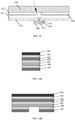
FIGS. 13A-13C show cross-sectional views of a back sheet of a photovoltaic module according to another embodiment of the present disclosure; -
FIGS. 14A-14B show cross-sectional views of a back sheet of a photovoltaic module according to another embodiment of the present disclosure; -
FIG. 15 shows a cross-sectional view of a back sheet of a photovoltaic module according to another embodiment of the present disclosure; -
FIG. 16 shows a cross-sectional view of a back sheet of a photovoltaic module according to another embodiment of the present disclosure; -
FIG. 17 shows a cross-sectional view of a back sheet of a photovoltaic module according to another embodiment of the present disclosure; -
FIG. 18 shows a cross-sectional view of a back sheet of a photovoltaic module according to another embodiment of the present disclosure; -
FIG. 19 shows a cross-sectional view of a back sheet of a photovoltaic module according to another embodiment of the present disclosure; -
FIG. 20 shows a cross-sectional view of a back sheet of a photovoltaic module according to another embodiment of the present disclosure; -
FIG. 21 shows a cross-sectional view of a back sheet of a photovoltaic module according to another embodiment of the present disclosure; -
FIG. 22 shows a cross-sectional view of a photovoltaic module according to another embodiment of the present disclosure; -
FIG. 23 shows a plan view of a thermally conductive layer inFIG. 22 ; -
FIG. 24 shows a cross-sectional view of a photovoltaic module according to another embodiment of the present disclosure; -
FIG. 25 shows a cross-sectional view of a photovoltaic module according to another embodiment of the present disclosure; -
FIG. 26 shows a cross-sectional view of a double-sided battery cell. - The photovoltaic module is usually plate-like or sheet-like, which substantially extend in a plane and have a certain thickness. In order to describe the photovoltaic module according to the present disclosure conveniently and clearly, the direction perpendicular to the plane in which the photovoltaic module extends is defined as the "thickness direction". In this specification, the "thermal communication" or "thermal connection" relationship between one component and another component includes not only the heat transfer relationship formed by the contact between the one component and the another component, but also the case in which an intermediate component is arranged between the one component and the another component and the heat of the one component is transferred to the another component. And the heat transfer includes not only heat conduction, but also heat radiation, heat convection, etc.
- The photovoltaic module generally includes a back sheet and a battery layer disposed on the back sheet. In the battery layer, a plurality of battery cells are arranged in an array. The battery cells can be single-sided battery cells or double-sided battery cells. The single-sided battery cell is a battery cell that can receive light from one side only and convert the light into electric power. The double-sided battery cell is a battery cell that can receive light from both sides and convert the light into electric power. The photovoltaic module including double-sided battery cells can not only receive direct sunlight from one side (i.e., the front side) to convert it into electric power, but also receive, from the other side (i.e., the back side), light such as reflected light or scattered light from the ground, thereby improving the power generation efficiency of the photovoltaic module. For example,
FIG. 26 shows a cross-sectional view of a double-sided battery cell. As shown in the figure, the double-sided battery cell includes a metalfront electrode 141, a frontanti-reflection film 142, a boron-dopedemission layer 143, an n-type silicon layer 144, a phosphorus-doped back surface field (BSF)layer 145, a backanti-reflection film 146 and ametal back electrode 147. And the battery cell can also have other configurations, without being limited in the present disclosure. - As mentioned above, hot spots that damage the photovoltaic module may occur in the photovoltaic module, and it is necessary to reduce the temperature of the photovoltaic module when hot spots occur, so as to improve the reliability of the photovoltaic module.
- A photovoltaic module uses a heat-dissipating aluminum back sheet structure to dissipate heat from the photovoltaic module. However, because the aluminum is opaque, when the photovoltaic module employs double-sided battery cells, the shielding of the aluminum layer will affect the power generation of the double-sided battery cells on its back side in the photovoltaic module.
- The photovoltaic module according to at least one embodiment of the present disclosure has a thermally conductive layer in a mesh shape, and the thermally conductive layer is in thermal communication with the battery layer and includes a skeleton section and a hollow section surrounded by the skeleton section. The skeleton section is made of or contains a thermally conductive material. In the thickness direction of the photovoltaic module, at least a part of the skeleton section of the thermally conductive layer overlaps with the gap between adjacent battery cells, and the hollow section of the thermally conductive layer overlaps with the battery cells. That is, at least a part of the skeleton section extends along the gap between adjacent battery cells, and the hollow section is provided at the battery cells. Therefore, on the one hand, heat generated by the battery cells can be conducted along the skeleton section of the thermally conductive layer, and on the other hand, light (such as reflected light and scattered light from the ground) can be allowed to pass through the hollow section of the thermally conductive layer from one side (back side) of the photovoltaic module to the other side (front side) of the photovoltaic module to be received by the back side of the battery cells, thereby reducing the influence on the illumination quantity of the back side of the photovoltaic module. While ensuring the back side power generation of the photovoltaic module which generates power on its both sides, the heat at the hot spot of the photovoltaic module is transferred out in time, and the temperature of the photovoltaic cell where the hot spot is formed is suppressed. Therefore, while ensuring the power generation efficiency of the photovoltaic module, the stability of the photovoltaic module is improved.
- It should be noted that the photovoltaic module according to some embodiments of the present disclosure is described by specially taking double-sided battery cells as an example, but the present disclosure is not limited thereto.
-
FIG. 1 shows a plan view of a photovoltaic module according to an embodiment of the present disclosure viewed from one side (front side),FIG. 2 shows a plan view of the photovoltaic module inFIG. 1 viewed from the other side (back side),FIG. 3 shows a cross-sectional view of the photovoltaic module inFIG. 1 ,FIG. 4 shows a plan view of a thermallyconductive layer 130 of the photovoltaic module inFIG. 1 , andFIG. 5 shows a plan view of aback sheet 110 of the photovoltaic module inFIG. 1 . InFIG. 1 , in order to clearly show theback sheet 110 and the thermallyconductive layer 130 disposed thereon, only theback sheet 110, the thermallyconductive layer 130 and thebattery layer 140 are shown (taking one battery cell in the battery layer as an example), and other components are omitted. InFIG. 2 , only thebattery layer 140 and the thermallyconductive layer 130 are shown, and other components are omitted. - As shown in
FIGS. 1-5 , the photovoltaic module according to an embodiment of the present disclosure includes aback sheet 110, a thermallyconductive layer 130 disposed on theback sheet 110, abattery layer 140 including a plurality of battery cells and disposed on the thermallyconductive layer 130, and afront sheet 150 covering thebattery layer 140. Thebattery layer 140 is bonded to thefront sheet 150 through asecond bonding layer 122 and is bonded to theback sheet 110 through afirst bonding layer 121, thus the photovoltaic module being packaged. The thermallyconductive layer 130 is bonded to theback sheet 110 through a thermally conductivelayer bonding layer 131. - For example, the
back sheet 110 and thefront sheet 150 can be glass plates, etc., or theback sheet 110 can be made of any other material, such as a high molecular polymer material. The high molecular polymer material can form, for example, an insulating barrier layer, a fluorine-containing weather-resistant layer, a third bonding layer or a bonding transition layer, etc. For example, thefirst bonding layer 121 and thesecond bonding layer 122 can be EVA (ethylene vinyl acetate) or POE (polyethylene-octene elastomer), etc. - The thermally
conductive layer 130 is in a mesh shape, and includes askeleton section 130a and ahollow section 130b surrounded by theskeleton section 130a, and theskeleton section 130a is formed of or contains a thermally conductive material. As shown inFIG. 3 , in the thickness direction of the photovoltaic module, at least a part of theskeleton section 130a overlaps with the gap between the battery cells and covers the edge portions of adjacent battery cells, so as to form thermal communication with the battery cells, while thehollow section 130b overlaps with the battery cells. In an embodiment, thehollow section 130b is filled with thefirst bonding layer 121. - On the one hand, when hot spots occur, the temperature of the battery cells with hot spots is, for example, above 105 Celsius degrees, while the temperature of the surrounding battery cells is usually, for example, at about 60 Celsius degrees. Due to the existence of temperature gradient, the heat will diffuse from the high temperature zone at the hot spots to the low temperature zone through the
skeleton section 130a of the thermallyconductive layer 130 in a heat conduction manner, thereby reducing the temperature at the hot spots. - On the other hand, light can pass through the
hollow section 130b of the thermallyconductive layer 130 and transmit through the photovoltaic module, so as to reduce the influence on the illumination quantity on the back side of the photovoltaic module, thereby ensuring the back side power generation of the photovoltaic module. - In the present embodiment, the
skeleton section 130a of the thermallyconductive layer 130 includes a plurality of first strip-shaped thermally conductive portions 132 extending in a first direction (up and down directions inFIGS. 1, 2 and4 ) and a plurality of second strip-shaped thermally conductive portions 133 extending in a second direction (left and right directions inFIGS. 1, 2 and4 ) perpendicular to the first direction, and the first strip-shaped thermally conductive portions 132 and the second strip-shaped thermally conductive portions 133 form a mesh shape. As shown inFIGS. 3-4 , in the thickness direction of the photovoltaic module, the first strip-shaped thermally conductive portion 132 or the second strip-shaped thermally conductive portion 133 of the thermallyconductive layer 130 overlaps with the gap between adjacent battery cells. That is, the first strip-shaped thermally conductive portion 132 and the second strip-shaped thermally conductive portion 133 are arranged to extend along the gap between adjacent battery cells, while thehollow portion 130b of the thermallyconductive layer 130 formed between the first strip-shaped thermally conductive portions 132 and the second strip-shaped thermally conductive portions 133 overlaps with the battery cells in the thickness direction. Therefore, the thermallyconductive layer 130 can conduct the heat at the battery cells, and reduce the influence on the light transmission through the photovoltaic module and the influence on the back side power generation efficiency of the photovoltaic module. - As shown in
FIG. 3 , in the present embodiment, in order to better conduct the heat at the battery cells of thebattery layer 140, the first strip-shaped thermally conductive portions 132 and the second strip-shaped thermally conductive portions 133 of the thermallyconductive layer 130 can be arranged to overlap with the edges of adjacent battery cells. However, those skilled in the art can understand that in other embodiments, the first strip-shaped thermally conductive portions 132 and the second strip-shaped thermally conductive portions 133 may not overlap with the edges of adjacent battery cells. - In some embodiments, in order to ensure a good heat conduction effect, the thickness of the thermally
conductive layer 130 can be in the range of 0.01-1 mm. In addition, the widths of the first strip-shaped thermally conductive portions 132 and the widths of the second strip-shaped thermally conductive portions 133 can be in the range of 5-50 mm. - In addition, the thermally
conductive layer 130 is further configured to be capable of reflecting light. Therefore, as shown inFIG. 3 , the light incident onto the thermallyconductive layer 130 can be reflected and then be incident onto the front side of the battery cells via, for example, the reflection of the back surface of thefront sheet 150, thereby enhancing the front side power generation efficiency of the photovoltaic module. For example, the thermallyconductive layer 130 is configured to be able to reflect at least 50%, at least 60%, at least 70%, at least 80% or at least 90% of light incident thereon. - For example, the thermally
conductive layer 130 can be made of a thermally conductive material, such as aluminum foil, copper foil, etc. In order to enhance the reflective performance of the thermallyconductive layer 130, the thermallyconductive layer 130 can be plated with tin or nickel. -
FIG. 6 shows a cross-sectional view of theskeleton section 130a of the thermallyconductive layer 130 and the thermally conductivelayer bonding layer 131 according to an embodiment of the present disclosure. The thermally conductivelayer bonding layer 131 is disposed between theback sheet 110 and the thermallyconductive layer 130. As shown inFIG. 6 , the thermally conductive layer 130 (specifically, theskeleton section 130a thereof) is bonded to theback sheet 110 through the thermally conductivelayer bonding layer 131. The surface of theskeleton section 130a of the thermallyconductive layer 130 facing thebattery layer 140 can be a planar surface.FIG. 7 shows a cross-sectional view of theskeleton section 130a of the thermallyconductive layer 130 and the thermally conductivelayer bonding layer 131 according to another embodiment of the present disclosure. As shown inFIG. 7 , the surface of theskeleton section 130a of the thermallyconductive layer 130 facing thebattery layer 140 can also be serrated, which serves as a prism to better reflect light to the battery cells of thebattery layer 140 and thereby increase the power generation efficiency of the front side of the photovoltaic module. - For example, the thermally conductive
layer bonding layer 131 can include EVA, POE, EAA, EEA (ethylene-ethyl acrylate), PP (polypropylene), SIS (styrene-isoprene-styrene), SBS (styrene-butadiene-styrene), etc. For example, the thermally conductivelayer bonding layer 131 can be EVA, POE or PP, which can be pressed onto theback sheet 110 at high temperature. Or, the thermally conductivelayer bonding layer 131 can be a blend resin of EVA, EAA (ethylene acrylic acid) and SIS, which can be pressed onto theback sheet 110 at high temperature. For example, such thermally conductivelayer bonding layer 131 can be hot-pressed together with thefirst bonding layer 121 and thesecond bonding layer 122 to form a photovoltaic module. Or, the thermally conductivelayer bonding layer 131 can be a blend resin of EVA, EEA and SBS, which can be pressed onto theback sheet 110 at low temperature or normal temperature. The present disclosure is not limited to these cases. - A manufacturing method for manufacturing, for example, the photovoltaic module as shown in
FIG. 3 , can include: S11, providing a back sheet; S12, laminating a thermally conductive layer on the back sheet; and S13, laminating a battery layer, which includes a plurality of battery cells, on the thermally conductive layer. The thermally conductive layer is in a mesh shape and includes a skeleton section and a hollow section surrounded by the skeleton section. The plurality of battery cells are arranged in an array. In the thickness direction of the photovoltaic module, at least a part of the skeleton section overlaps with the gap between adjacent battery cells, and the hollow section overlaps with the battery cells. - The thermally
conductive layer 130 in the embodiment shown inFIGS. 1-5 can be formed by various ways. In one embodiment, the first strip-shaped thermally conductive portions 132 and the second strip-shaped thermally conductive portions 133 are respectively bonded onto theback sheet 110, so as to form a thermally conductive layer. For example, a rolled strip of aluminum foil can be unfolded and attached to theback sheet 110 to form a first strip-shaped thermally conductive portion 132, and then a rolled strip of aluminum foil can be unfolded and attached to theback sheet 110 to form a second strip-shaped thermally conductive portion 133; the first strip-shaped thermally conductive portion 132 and the second strip-shaped thermally conductive portion 133 intersects with each other to form a mesh pattern, thereby forming askeleton section 130a of the thermallyconductive layer 130, while the section surrounded by the first strip-shaped thermally conductive portion 132 and the second strip-shaped thermally conductive portion 133 forms ahollow section 130b of the thermallyconductive layer 130. For example, the first strip-shaped thermally conductive portion 132 and the second strip-shaped thermally conductive portion 133 can have the same width. Therefore, the first strip-shaped thermally conductive portion 132 and the second strip-shaped thermally conductive portion 133 can be formed by using the same rolled strip, thus reducing the cost and facilitating the manufacturing. The first strip-shaped thermally conductive portion 132 and the second strip-shaped thermally conductive portion 133 may have different widths as needed. - In another embodiment, the pattern composed of the
skeleton section 130a and thehollow section 130b of the thermallyconductive layer 130 can also be formed by stamping a sheet material. However, the present invention is not limited to these cases, and the thermally conductive layer can also be formed on theback sheet 110 by other means such as screen printing, coating, spray coating, sintering, etc. - The thermally
conductive layer 130 shown inFIG. 4 has a rectangular mesh pattern, but the present disclosure is not limited thereto.FIGS. 8-10 show plan views of the thermallyconductive layer 130 according to other embodiments of the present disclosure. As shown inFIG. 8 , the thermallyconductive layer 130 is in a cross-and-saltire-shaped mesh pattern. As shown inFIG. 9 , the thermallyconductive layer 130 is in a honeycomb mesh pattern. As shown inFIG. 10 , the thermallyconductive layer 130 is in a grid-like mesh pattern. In the patterns as shown inFIGS. 8-10 , askeleton section 130a overlapping with the battery cells is added on the basis of the first strip-shaped thermally conductive portions 132 and the second strip-shaped thermally conductive portions 133 as shown inFIG. 4 . The rectangular mesh pattern shown inFIG. 4 has less influence on the back side power generation efficiency of the photovoltaic module, while the overlapping area between the thermallyconductive layer 130 and the battery cells shown inFIGS. 8-10 is larger, so that the thermally conductive efficiency is higher. The specific pattern of the thermallyconductive layer 130 can be designed according to different needs. - The thermally
conductive layer 130 shown inFIG. 10 is in a grid-like mesh pattern, the light shielding region where theskeleton section 130a overlaps with the battery cells includes a plurality of sub-strip-shaped thermallyconductive portions 134, and the plurality of sub-strip-shaped thermallyconductive portions 134 preferably overlap with the main grids of the battery cells. As the plurality of sub-strip-shaped thermallyconductive portions 134 overlap with the main grids of the battery cells, they can quickly conduct the heat at the main grid, thereby minimizing the melting phenomenon of solder at the main grids caused by local overheating. Here, the main grid is a bus line connected with the fine grids (e.g., the front electrode and the back electrode of the battery cell) to collect current from the fine grids. - The photovoltaic module can also have other laminated structures.
-
FIG. 11 shows a cross-sectional view of a photovoltaic module according to another embodiment of the present disclosure. As shown inFIG. 11 , the photovoltaic module includes aback sheet 210, afirst bonding layer 221 disposed on a first surface of theback sheet 210, abattery layer 240 including a plurality of battery cells and disposed on thefirst bonding layer 221, asecond bonding layer 222 covering thebattery layer 240, afront sheet 250 disposed on thesecond bonding layer 222, and a thermallyconductive layer 230 disposed on a second surface of theback sheet 210 opposite to the first surface of theback sheet 210. The thermallyconductive layer 230 is bonded to theback sheet 210 through a thermally conductivelayer bonding layer 231. In order to increase the thermally conductive efficiency of the thermallyconductive layer 230, in the thickness direction, the skeleton section of the thermallyconductive layer 230 overlaps with the edge of the battery cell adjacent thereto. Optionally, because the thermallyconductive layer 230 is exposed to the atmosphere, in order to protect the thermallyconductive layer 230, afluororesin layer 260 serving as a protective layer can be disposed, for example, by spraying, on a side of the thermallyconductive layer 230 away from theback sheet 210. -
FIG. 12 shows a cross-sectional view of a photovoltaic module according to another embodiment of the present disclosure. As shown inFIG. 12 , the photovoltaic module includes aback sheet 310, afirst bonding layer 321 disposed on a first surface of theback sheet 310, abattery layer 340 including a plurality of battery cells and disposed on thefirst bonding layer 321, asecond bonding layer 322 covering thebattery layer 340, afront sheet 350 disposed on thesecond bonding layer 322, and a thermallyconductive layer 330 disposed on a second surface of theback sheet 310 opposite to the first surface of theback sheet 310. The thermallyconductive layer 330 is bonded to theback sheet 310 through a thermally conductivelayer bonding layer 331. In order to increase the thermally conductive efficiency of the thermallyconductive layer 330, in the thickness direction, the skeleton section of the thermallyconductive layer 330 overlaps with the edge of the battery cell adjacent thereto. Different from the photovoltaic module shown inFIG. 11 , in order to protect the thermallyconductive layer 330, a fluorine-containing weather-resistant layer 380 serving as a protective layer can be disposed on a side of the thermallyconductive layer 330 away from theback sheet 310, and the fluorine-containing weather-resistant layer 380 is attached to the thermallyconductive layer 330 through afourth bonding layer 370. For example, thefourth bonding layer 370 can be polyurethane, EVA, POE, PP, or blend resin of EVA, EAA and SIS, or blend resin of EVA, EEA and SBS. - A manufacturing method for manufacturing, for example, the photovoltaic modules as shown in
FIG. 11 andFIG. 12 can include: S21, providing a back sheet; S22, laminating a battery layer on a first side of the back sheet; and S23, laminating a thermally conductive layer on a second side of the back sheet opposite to the first side of the back sheet. The battery cells are arranged in an array. The thermally conductive layer is in a mesh shape and includes a skeleton section and a hollow section surrounded by the skeleton section. In the thickness direction of the photovoltaic module, at least a part of the skeleton section overlaps with the gap between adjacent battery cells, and the hollow section overlaps with the battery cells. -
FIGS. 13A-21 respectively show cross-sectional views of a back sheet of a photovoltaic module according to another embodiment of the present disclosure. As shown inFIGS. 13A-21 , the thermally conductive layer can also be compounded into the back sheet instead of being disposed on the back sheet independently of the back sheet. In the embodiment shown inFIGS. 13A-21 , the thermally conductive layer in the back sheet is in a mesh shape, and the battery layer including a plurality of battery cells is disposed on the back sheet. At least a part of the skeleton section of the thermally conductive layer overlaps with the gap between adjacent battery cells and the edge of the battery cell adjacent thereto in the thickness direction, while the hollow section of the thermally conductive layer overlaps with the battery cells in the thickness direction. - As shown in
FIG. 13A , in an example, the back sheet can sequentially include a thermallyconductive layer 407, a firstthird bonding layer 406, a fluorine-containing weather-resistant layer 405, a secondthird bonding layer 404, an insulatingbarrier layer 403, a thirdthird bonding layer 402 and abonding transition layer 401, which are stacked. For example, the battery layer can be attached to thebonding transition layer 401 through a first bonding layer (e.g., thefirst bonding layer 121 as shown inFIG. 3 ). The bonding transition layer is disposed at the outermost side of the back sheet, here, at the outer side of the thirdthird bonding layer 402, and this is helpful to enhance the bonding force of the first bonding layer to the back sheet, so that the back sheet and the battery layer are more firmly bonded together. As shown inFIG. 13B andFIG. 13C , because the thermallyconductive layer 407 is in a mesh shape and includes a skeleton section and a hollow section, the hollow section can be filled with air (seeFIG. 13B ) or be filled with the firstthird bonding layer 406 adjacent thereto (seeFIG. 13C ). - As shown in
FIG. 14A , in another example, the back sheet can sequentially include a fluorine-containing weather-resistant layer 507, a firstthird bonding layer 506, an insulatingbarrier layer 505, a secondthird bonding layer 504, a thermallyconductive layer 503, a thirdthird bonding layer 502 and abonding transition layer 501, which are stacked. For example, the battery layer can be attached to thebonding transition layer 501 through a first bonding layer (e.g., thefirst bonding layer 121 as shown inFIG. 3 ). As shown inFIG. 14B , because the thermallyconductive layer 503 is in a mesh shape and includes a skeleton section and a hollow section, the hollow section can be filled with the thirdthird bonding layer 502 adjacent thereto and/or the secondthird bonding layer 504 adjacent thereto. - As shown in
FIG. 15 , in another example, the back sheet can sequentially include a fluorine-containing weather-resistant layer 607, a firstthird bonding layer 606, a thermallyconductive layer 605, a secondthird bonding layer 604, an insulatingbarrier layer 603, a thirdthird bonding layer 602 and abonding transition layer 601, which are stacked. For example, the battery layer can be attached to thebonding transition layer 601 through a first bonding layer (e.g., thefirst bonding layer 121 as shown inFIG. 3 ). - As shown in
FIG. 16 , in another example, the back sheet can sequentially include a fluorine-containing weather-resistant layer 706, a firstthird bonding layer 705, an insulatingbarrier layer 704, a secondthird bonding layer 703, a thermally conductive layer 702 and abonding transition layer 701, which are stacked. For example, the battery layer can be attached to thebonding transition layer 701 through a first bonding layer (e.g., thefirst bonding layer 121 as shown inFIG. 3 ). The bonding transition layer is disposed at the outermost side of the back sheet, here, at the outer side of the thermally conductive layer 702, and this is helpful to enhance the bonding force of the first bonding layer to the back sheet, so that the back sheet and the battery layer are more firmly bonded together. - As shown in
FIG. 17 , in another example, the back sheet can sequentially include a fluorine-containing weather-resistant layer 806, a firstthird bonding layer 805, a thermallyconductive layer 804, a secondthird bonding layer 803, an insulating barrier layer 802 and abonding transition layer 801, which are stacked. For example, the battery layer can be attached to thebonding transition layer 801 through a first bonding layer (e.g., thefirst bonding layer 121 shown inFIG. 3 ). The bonding transition layer is arranged at the outermost side of the back sheet, here, at the outer side of the insulating barrier layer 802, and this is helpful to enhance the bonding force of the first bonding layer to the back sheet, so that the back sheet and the battery layer are more firmly bonded together. - As shown in
FIG. 18 , in another example, the back sheet can sequentially include a thermallyconductive layer 906, a firstthird bonding layer 905, a fluorine-containing weather-resistant layer 904, a secondthird bonding layer 903, an insulatingbarrier layer 902 and abonding transition layer 901, which are stacked. For example, the battery layer can be attached to thebonding transition layer 901 through a first bonding layer (e.g., thefirst bonding layer 121 as shown inFIG. 3 ). - As shown in
FIG. 19 , in another example, the back sheet can sequentially include a fluorine-containing weather-resistant layer 1005, a thermallyconductive layer 1004, athird bonding layer 1003, an insulatingbarrier layer 1002 and abonding transition layer 1001, which are stacked. For example, the battery layer can be attached to thebonding transition layer 1001 through a first bonding layer (e.g., thefirst bonding layer 121 as shown inFIG. 3 ). - As shown in
FIG. 20 , in another example, the back sheet can sequentially include a fluorine-containing weather-resistant layer 1105, an insulatingbarrier layer 1104, athird bonding layer 1103, a thermallyconductive layer 1102 and abonding transition layer 1101, which are stacked. For example, the battery layer can be attached to thebonding transition layer 1101 through a first bonding layer (e.g., thefirst bonding layer 121 as shown inFIG. 3 ). - As shown in
FIG. 21 , in another example, the back sheet can sequentially include a thermallyconductive layer 1205, athird bonding layer 1204, a fluorine-containing weather-resistant layer 1203, an insulatingbarrier layer 1202 and abonding transition layer 1201, which are stacked. For example, the battery layer can be attached to thebonding transition layer 1201 through a first bonding layer (e.g., thefirst bonding layer 121 as shown inFIG. 3 ). - In the examples shown in
FIGS. 19-21 , the back sheet adopts a five-layer structure. While ensuring other performances of the back sheet, the back sheet has fewer layers and is thin as a whole, and therefore, the thermallyconductive layers - For example, the fluorine-containing weather-resistant layer can be a fluorine film, such as PVDF (polyvinylidene fluoride) film, TEDLAR (registered trademark) film (polyvinyl fluoride film), fluorocarbon resin, etc. For example, the third bonding layer in the back sheet can be polyurethane, etc. For example, the insulating barrier layer can be PET (polyethylene terephthalate), etc. For example, the bonding transition layer can be EVA, POE, LDPE (Low Density Polyethylene), PVDF film, TEDLAR film (e.g., as shown in
FIGS. 13A-15 ), or can be fluororesin, such as fluorocarbon resin (e.g., as shown inFIGS. 16-21 ), etc. - A manufacturing method for manufacturing, for example, the photovoltaic modules as shown in
FIG. 13 andFIG. 21 can include: S31, providing a back sheet; and S32, laminating battery cells in an array on the back sheet. The thermally conductive layer is in a mesh shape and includes a skeleton section and a hollow section surrounded by the skeleton section, and in the thickness direction of the photovoltaic module, at least a part of the skeleton section overlaps with the gap between adjacent battery cells, and the hollow section overlaps with the battery cells. The step S31 of providing the back sheet includes, for example, laminating the thermally conductive layer with at least one selected from the group consisting of the insulating barrier layer, the fluorine-containing weather-resistant layer and the bonding transition layer to form the back sheet. According to the present embodiment, the thermally conductive layer can be formed together with the back sheet in the manufacturing process of the back sheet, thus reducing the manufacturing cost. - In the examples as shown in
FIGS. 13A-21 , the thermallyconductive layers FIGS. 13A-21 , the thermallyconductive layers conductive layers conductive layers - It should be understood by those skilled in the art that the structure of the back sheet, such as those shown in
FIGS. 13A-21 , can also be applied to the thermally conductive layer with other patterns, and are not limited to the thermally conductive layer in the mesh shape, and for example, can be applied to a thermally conductive layer without the hollow section but with a complete surface, such as the thermally conductive layer as shown inFIG. 23 to be described below. - The photovoltaic module according to another embodiment of the present disclosure includes a back sheet, a thermally conductive layer, a battery layer and a front sheet. For example, in an example, similar to the photovoltaic module shown in
FIG. 3 (but not including the thermal conductive layer bonding layer 131), the photovoltaic module can include a back sheet, a thermal conductive layer disposed on the back sheet, a battery layer including a plurality of battery cells and disposed on the thermal conductive layer, and a front sheet covering the battery layer. For example, in another example, similar to the photovoltaic modules shown inFIGS. 11-12 (but not including the thermally conductive layer bonding layers 231 and 331) andFIGS. 22 and24 to be described below, the photovoltaic module can include a back sheet, a battery layer including a plurality of battery cells and disposed on the back sheet, a front sheet covering the battery layer, and a thermally conductive layer disposed on a side of the back sheet away from the battery layer. For example, the thermally conductive layer is in a mesh shape and includes a skeleton section and a hollow section surrounded by the skeleton section, and in the thickness direction of the photovoltaic module, at least a part of the skeleton section overlaps with the gap between adjacent battery cells, and the hollow section overlaps with the battery cells. - In the present embodiment, the thermally conductive layer is a thermally conductive film layer bonded to a surface of the back sheet, and the thermally conductive film layer includes thermally conductive particles and a white inorganic pigment. The thermally conductive particles in the thermally conductive film layer provide the thermally conductive film layer a good thermally conductive characteristic, so as to conduct out the heat of the battery layer at the hot spot in time. The white inorganic pigment in the thermally conductive film layer provides the thermally conductive layer a good reflective characteristic, so as to reflect light incident on the thermally conductive layer to the battery cells, thereby increasing the power generation efficiency of the photovoltaic module.
- For example, the thermally conductive particles can include one or more selected from the group consisting of silicon carbide, aluminum nitride and boron carbide. In addition, the thermally conductive particles can also include one or more selected from the group consisting of aluminum particles, silver particles, copper particles and gold particles.
- For example, the white inorganic pigment can include one or more selected from the group consisting of lithopone, titanium dioxide, talcum powder, lead white, mica, calcium carbonate, calcium sulfate, zinc oxide, antimony trioxide, magnesium oxide, magnesium carbonate, iron oxide, silicon dioxide, zirconium dioxide, barium sulfate and aluminum oxide.
- In addition, the thermally conductive layer can further include a binder, an assistant or a catalyst.
- The binder is used to firmly attach the thermally conductive layer to the back sheet, such as a glass back sheet. The binder can include an organic polymer, or a colloid formed from organic salt, inorganic salt or organometallic compound. For example, the organic salt can be an alkoxide of Ti(OR)4 or Si(OR)4, or Pb(CH3COO)2. For example, the inorganic salt can be Zn(NO3)2 or zirconium oxychloride. For example, the organic polymer can include phenolic resin, urea-formaldehyde resin, epoxy resin, polyvinyl acetate, polyethylene-ethyl vinyl ester, acrylate, polystyrene, alkyd resin, polyurethane, polyisocyanate, acrylate diester, silane, polybenzimidazole, polyimide or butyl rubber.
- The assistant is used to improve the stability of the thermally conductive film layer and other characteristics thereof. For example, the assistant can be one or more selected from the group consisting of emulsifier, dispersant, polymerization inhibitor, rheological agent, anti-settling agent, desiccant, anti-scaling agent, anti-shrinkage agent, anti-scratch agent, antioxidant, lubricant, release agent, heat stabilizer, light stabilizer, antistatic agent, anti-wear agent, thickener and defoamer. The catalyst can be one or more selected from the group consisting of inorganic acid, organic acid, alkali, acid salt, basic salt and organic ammonium salt.
- The white inorganic pigment and the thermally conductive particles are mixed with reagents and solvents, such as the binder, the assistant and the catalyst, etc., so as to prepare a thermally conductive layer preform. The thermally conductive layer preform is coated on the back sheet by screen printing, roll coating, spray coating, draw coating, spin coating, slit method (a coating method of extruding the solution along the die gap and transferring it to a moving substrate), ultrasonic atomization, or any combination thereof. Then, the thermally conductive layer preform is dried at a suitable temperature to form a back sheet attached with the thermally conductive layer. For example, the drying temperature can be, for example, in the range of 0-800 Celsius degrees, or in the range of 0-60 Celsius degrees. Here, the back sheet can include a glass layer. For example, the solvent can be water, petroleum solvent, benzene solvent, terpene solvent, alcohol solvent, ether solvent, ketone solvent, ester solvent, chlorinated hydrocarbon solvent, nitro hydrocarbon solvent or amine solvent.
- The thermally conductive film layer can be attached to the back sheet by coating, so it is convenient to manufacture and low in cost, and the manufacturing process of the thermally conductive layer can be combined into the manufacturing process of the back sheet, thus being convenient for management.
- In the above embodiments, the thermally conductive layer is in a mesh shape. In some other embodiments, the photovoltaic module includes a back sheet, a thermally conductive layer, a battery layer and a front sheet, and the thermally conductive layer can be disposed, for example, substantially over the entire surface of the back sheet. Similar to the above embodiments, the thermally conductive layer is a thermally conductive film layer bonded to substantially the entire surface of the back sheet, and the thermally conductive film layer includes thermally conductive particles and a white inorganic pigment. The thermally conductive particles in the thermally conductive film layer provide the thermally conductive film layer a good thermally conductive characteristic, so as to conduct out the heat of the battery layer at the hot spot in time. The white inorganic pigment in the thermally conductive film layer provides the thermally conductive layer a good reflective characteristic, so as to reflect light incident on the thermally conductive layer to the battery cells, thereby increasing the power generation efficiency of the photovoltaic module. Other aspects of the thermally conductive layer can be configured as those in the above embodiments.
-
FIG. 22 shows a cross-sectional view of a photovoltaic module according to another embodiment of the present disclosure. As shown inFIG. 22 , the photovoltaic module includes a laminated structure and a thermallyconductive layer 130. The laminated structure includes afront sheet 150, afirst bonding layer 122, abattery layer 140, asecond bonding layer 121 and aback sheet 110. Thebattery layer 140 includes a plurality of battery cells arranged in an array and configured to receive light and generate power. Thebattery layer 140 is bonded to thefront sheet 150 through thefirst bonding layer 122 and to theback sheet 110 through thesecond bonding layer 121, and then the laminated structure is formed by laminating thefront sheet 150, thefirst bonding layer 122, thebattery layer 140, thesecond bonding layer 121 and theback sheet 110. The thermallyconductive layer 130 is formed on the surface of theback sheet 110 on a side away from thebattery layer 140. Therefore, the thermallyconductive layer 130 can be formed on the outer surface of the laminated structure after the laminated structure is formed. Therefore, the forming step of the thermallyconductive layer 130 can be conveniently and economically combined with the existing manufacturing line. In addition, after the photovoltaic module is put into use, maintenance and service (e.g., repair) of the thermallyconductive layer 130 can be convenient. - For example, the
front sheet 150 can be a transparent glass plate. Theback sheet 110 can be a glass plate, or a composite plate including, for example, an insulating barrier layer, a fluorine-containing weather-resistant layer, a third bonding layer and a bonding transition layer. - A manufacturing method for manufacturing, for example, the photovoltaic module as shown in
FIG. 22 can include: providing atransparent front sheet 150; providing aback sheet 110; providing abattery layer 140 between thefront sheet 150 and theback sheet 110; laminating a stacked structure which includes thefront sheet 150, thebattery layer 140 and theback sheet 110, so as to form a laminated structure; and after the laminating, providing a thermallyconductive layer 130 on the surface of theback sheet 110 on a side away from thebattery layer 140. - Specifically, providing the thermally
conductive layer 130 can include coating a thermally conductive layer solution containing thermally conductive particles on the surface of theback sheet 110 on a side away from thebattery layer 140; and drying the thermally conductive layer solution to form the thermallyconductive layer 130. - For example, the thermally conductive particles can include one or more selected from the group consisting of aluminum particles, silver particles, copper particles and gold particles. These metal particles have good thermal conductivity and are easy to be uniformly coated. In addition, the thermally conductive particles can also include silicon carbide, aluminum nitride, boron carbide, etc.
- In the present example, the thermally
conductive layer 130 is provided on the surface of theback sheet 110 on a side away from thebattery layer 140, and is provided after the laminating. However, it should be understood by those skilled in the art that such method of providing the thermallyconductive layer 130 can be applied to the case in which the thermallyconductive layer 130 is provided on the surface of the back sheet on a side closer to thebattery layer 140, and can be performed before the laminating. In addition, in some other examples, the thermally conductive layer solution can also include the above-mentioned white pigment, etc. - In the present example, the thermally conductive layer solution includes curing component and diluting component. The curing components can include rheological assistant, acrylic resin, amino resin, first solvent, acetate butyrate fiber solution and leveling agent. The diluting component can include second solvent and isocyanate. The rheological assistant has an alignment effect on aluminum particles, and can be, for example, ethylene-vinyl acetate copolymer dispersion or polyolefin anti-settling agent. The first solvent can be, for example, an alcohol ether organic solvent containing hydrophilic groups and lipophilic groups. The second solvent can be aliphatic, ketone, glycol, glycol ether, glycol ester or aromatic hydrocarbon solvent.
- For example, the thermally conductive layer solution can be coated on the surface of the
back sheet 110 by any one of screen printing, roll coating, spray coating, draw coating, spin coating, slit method, ultrasonic atomization, or any combination thereof. - In addition, the manufacturing method can further include: providing a
first bonding layer 122; and providing asecond bonding layer 121. And the above laminating step is to laminate a stacked structure including thefront sheet 150, thefirst bonding layer 122, thebattery layer 140, thesecond bonding layer 121 and theback sheet 110 in sequence. - In the present embodiment, the thermally conductive layer solution is directly coated on the laminated structure including the
front sheet 150, theback sheet 110 and thebattery layer 140, so as to form the thermallyconductive layer 130. Therefore, the photovoltaic module with the thermallyconductive layer 130 can be formed by directly adding a manufacturing process of the thermallyconductive layer 130 to the existing production process, so that the manufacturing process of the thermallyconductive layer 130 can be combined with the existing process conveniently and at low cost. In addition, because the thermallyconductive layer 130 is directly formed on the laminated structure instead of inside the laminated structure, it is convenient for the long-term maintenance of the photovoltaic module in the later period. Moreover, the thermallyconductive layer 130 is formed by coating the thermally conductive layer solution and drying the thermally conductive layer solution, which simplifies the manufacturing and later maintenance of the thermallyconductive layer 130 on the laminated structure, and reduces the manufacturing cost of the photovoltaic module. -
FIG. 23 shows a plan view of the thermallyconductive layer 130 inFIG. 22 . As shown inFIG. 23 , the thermallyconductive layer 130 can cover substantially the entire surface of theback sheet 110. However, the pattern of the thermallyconductive layer 130 is not limited thereto, and for example, the thermallyconductive layer 130 can be in a mesh shape. In the case where the thermallyconductive layer 130 is in a mesh shape, the cross-sectional view of the photovoltaic module is, for example, as shown inFIG. 24 . -
FIG. 25 shows a cross-sectional view of a photovoltaic module according to another embodiment of the present disclosure. As shown inFIG. 25 , different from the embodiment shown inFIG. 22 , in the present embodiment, the thermallyconductive layer 130 is bonded to the surface of theback sheet 110 on a side away from thebattery layer 140 through a thermally conductivelayer bonding layer 131. As shown inFIG. 25 , the photovoltaic module includes afront sheet 150, afirst bonding layer 122, abattery layer 140, asecond bonding layer 121, aback sheet 110, a thermally conductivelayer bonding layer 131 and a thermallyconductive layer 130. - Because the thermally conductive layer is formed on the surface of the
back sheet 110 on a side away from thebattery layer 140, maintenance and service (e.g., repair) of the thermallyconductive layer 130 can be convenient after the photovoltaic module is put into use. - The thermally
conductive layer 130 can be, for example, a sheet containing thermally conductive particles, such as a foil of aluminum, silver, gold, copper or alloys thereof. In the embodiment shown inFIG. 25 , similar to the thermallyconductive layer 130 as shown inFIG. 23 , the thermallyconductive layer 130 can cover substantially the entire surface of theback sheet 110. However, it should be understood by those skilled in the art that the thermallyconductive layer 130 can have other patterns. - In an embodiment, a manufacturing method for manufacturing, for example, the photovoltaic module as shown in
FIG. 25 can include: providing atransparent front sheet 150; providing aback sheet 110; providing abattery layer 140 between thefront sheet 150 and theback sheet 110; laminating a stacked structure which includes thefront sheet 150, thebattery layer 140 and theback sheet 110, so as to form a laminated structure; and after the laminating, providing a thermallyconductive layer 130 on the surface of theback sheet 110 on a side away from thebattery layer 140. Specifically, providing the thermally conductive layer includes: bonding the thermallyconductive layer 330 to the surface of theback sheet 110 on a side away from thebattery layer 140 through the thermally conductivelayer bonding layer 131. - For example, here, the thermally conductive
layer bonding layer 131 can be epoxy resin, acrylic resin, amino resin or silicone. Such thermally conductivelayer bonding layer 131 can bond the thermallyconductive layer 130, such as aluminum foil, to theback sheet 110 at normal temperature, which facilitates the formation of the thermallyconductive layer 130. In addition, the thermallyconductive layer 130 is formed after the laminating, and therefore, the photovoltaic module with the thermallyconductive layer 130 can be formed by directly adding a manufacturing process of the thermallyconductive layer 130 to the existing production process, so that the manufacturing process of the thermallyconductive layer 130 can be combined with the existing process conveniently and at low cost. - In an embodiment, a manufacturing method for manufacturing, for example, the photovoltaic module as shown in
FIG. 25 can include: providing atransparent front sheet 150; providing aback sheet 110; providing abattery layer 140 between thefront sheet 150 and theback sheet 110; providing a thermallyconductive layer 130; providing a thermally conductivelayer bonding layer 131 between the thermallyconductive layer 130 and the surface of theback sheet 110 away from thebattery layer 140; and laminating a stacked structure which sequentially includes thefront sheet 150, thebattery layer 140, theback sheet 110, the thermally conductivelayer bonding layer 131 and the thermallyconductive layer 130. Here, in the laminating process, the thermally conductivelayer bonding layer 131 is melted due to high temperature, and the thermallyconductive layer 130 is bonded to theback sheet 110 by hot melt welding using the thermally conductivelayer bonding layer 131. For example, here, the thermally conductivelayer bonding layer 131 can be a photovoltaic module packaging film, such as EVA or POE, or any other bonding material, as long as the laminating temperature range of the thermally conductivelayer bonding layer 131 is the same as those of the materials of thefirst bonding layer 122 and thesecond bonding layer 121 and it is convenient for being laminated together. - In addition, a
first bonding layer 122 can be provided between thefront sheet 150 and thebattery layer 140, and asecond bonding layer 121 can be provided between theback sheet 110 and thebattery layer 140, and thefirst bonding layer 122 and thesecond bonding layer 121 can be laminated simultaneously in the laminating process. - Here, the
front sheet 150, thefirst bonding layer 122, thebattery layer 140, thesecond bonding layer 121, theback sheet 110, the thermally conductive layer bonding layer 3113 and the thermallyconductive layer 130 are laminated together at the same time, so as to form a photovoltaic module, and this is helpful to simplify the manufacturing process of the photovoltaic module and reduce the manufacturing cost, and is helpful to economically and conveniently combine the formation of the thermallyconductive layer 130 with the existing manufacturing process. - This specification describes at least the following items:
- (1) A photovoltaic module, comprising:
- a battery layer, wherein the battery layer comprises a plurality of battery cells, and the plurality of battery cells are arranged in an array and configured to receive light and generate power; and
- a thermally conductive layer, wherein the thermally conductive layer is formed of a thermally conductive material or contains a thermally conductive material, and is in thermal communication with the battery layer,
- wherein the thermally conductive layer is in a mesh shape and comprises a skeleton section and a hollow section surrounded by the skeleton section; and in a thickness direction of the photovoltaic module, at least a part of the skeleton section overlaps with a gap between adjacent battery cells, and the hollow section overlaps with the plurality of battery cells.
- (2) The photovoltaic module according to item (1), further comprising a back sheet, wherein the thermally conductive layer is sandwiched between the back sheet and the battery layer.
- (3) The photovoltaic module according to item (1), further comprising a back sheet, wherein the thermally conductive layer is disposed on a side of the back sheet away from the battery layer.
- (4) The photovoltaic module according to item (2) or (3), further comprising a thermally conductive layer bonding layer, wherein the thermally conductive layer bonding layer is disposed between the back sheet and the thermally conductive layer so as to bond the thermally conductive layer to the back sheet.
- (5) The photovoltaic module according to item (2) or (3), further comprising a first bonding layer, wherein the first bonding layer is disposed between the back sheet and the battery layer so as to bond the battery layer to the back sheet.
- (6) The photovoltaic module according to any one of items (1)-(5), wherein
the skeleton section of the thermally conductive layer is configured to be capable of reflecting light. - (7) The photovoltaic module according to any one of items (1)-(6), wherein
the skeleton section of the thermally conductive layer is aluminum foil or copper foil. - (8) The photovoltaic module according to any one of items (1)-(7), wherein
the skeleton section of the thermally conductive layer is plated with tin or nickel. - (9) The photovoltaic module according to any one of items (1)-(8), wherein
a surface, facing the battery layer, of the skeleton section of the thermally conductive layer is serrated. - (10) The photovoltaic module according to any one of items (1)-(9), wherein
in the thickness direction, the at least a part of the skeleton section overlaps with an edge of the battery cell. - (11) The photovoltaic module according to any one of items (1)-(10), wherein
the skeleton section comprises a plurality of first strip-shaped thermally conductive portions extending in a first direction and a plurality of second strip-shaped thermally conductive portions extending in a second direction intersected with the first direction. - (12) The photovoltaic module according to item (11), wherein
the first direction is perpendicular to the second direction. - (13) The photovoltaic module according to item (11) or (12), wherein the first strip-shaped thermally conductive portion and the second strip-shaped thermally conductive portion have a same width.
- (14) The photovoltaic module according to any one of items (1)-(13), wherein
the thermally conductive layer is formed by stamping a sheet material. - (15) The photovoltaic module according to any one of items (1)-(14), wherein
the thermally conductive layer is in a grid-like mesh pattern, the skeleton section comprises a plurality of sub-strip-shaped thermally conductive portions overlapped with the battery cells, and the plurality of sub-strip-shaped thermally conductive portions overlap with main grids of the battery cells. - (16) The photovoltaic module according to item (3), further comprising:
a protective layer, wherein the protective layer is disposed on a side of the thermally conductive layer away from the back sheet. - (17) The photovoltaic module according to item (2) or (3), further comprising:
a front sheet, wherein the front sheet is disposed on a side of the battery layer away from the back sheet, and the battery layer is sandwiched between the back sheet and the front sheet. - (18) The photovoltaic module according to item (2) or (3), wherein the thermally conductive layer is a thermally conductive film layer bonded to a surface of the back sheet, and the thermally conductive film layer comprises a thermally conductive particle and a white inorganic pigment.
- (19) The photovoltaic module according to item (18), wherein the thermally conductive particle comprises one or more selected from a group consisting of silicon carbide, aluminum nitride and boron carbide.
- (20) The photovoltaic module according to item (18), wherein the white inorganic pigment comprises one or more selected from a group consisting of lithopone, titanium dioxide, talcum powder, lead white, mica, calcium carbonate, calcium sulfate, zinc oxide, antimony trioxide, magnesium oxide, magnesium carbonate, iron oxide, silicon dioxide, zirconium dioxide, barium sulfate and aluminum oxide.
- (21) The photovoltaic module according to any one of items (2), (3) and (18), wherein the back sheet comprises a glass layer.
- (22) The photovoltaic module according to item (2) or (3), wherein
the back sheet comprises at least one selected from a group consisting of an insulating barrier layer, a fluorine-containing weather-resistant layer, a third bonding layer and a bonding transition layer. - (23) A back sheet of a photovoltaic module, comprising:
a thermally conductive layer in a mesh shape, wherein the thermally conductive layer comprises a skeleton section and a hollow section surrounded by the skeleton section. - (24) The back sheet according to item (23), further comprising:
- a third bonding layer; and
- at least one selected from a group consisting of an insulating barrier layer, a fluorine-containing weather-resistant layer and a bonding transition layer,
- wherein the thermally conductive layer is adjacent to at least one of the third bonding layers.
- (25) The back sheet according to item (23), further comprising:
- a third bonding layer, an insulating barrier layer, a fluorine-containing weather-resistant layer and a bonding transition layer,
- wherein the thermally conductive layer is adjacent to at least one of the third bonding layers.
- (26) The back sheet according to item (23), wherein
- the back sheet comprises five layers and further comprises: a third bonding layer, an insulating barrier layer, a fluorine-containing weather-resistant layer, and a bonding transition layer at outermost; and
- the thermally conductive layer is adjacent to at least one of the third bonding layers.
- (27) The back sheet according to any one of items (24)-(26), wherein the third bonding layer extends into the hollow section of the thermally conductive layer.
- (28) The back sheet according to item (23), wherein
the thermally conductive layer comprises a polymeric resin and thermally conductive particles mixed in the polymeric resin. - (29) The back sheet according to item (28), further comprising:
- an insulating barrier layer, wherein
- the thermally conductive layer is adjacent to the insulating barrier layer, and the thermally conductive layer and the insulating barrier layer are formed together by co-extrusion.
- (30) The back sheet according to item (29), wherein
the insulating barrier layer comprises the polymeric resin, and the polymeric resin is PET. - (31) A photovoltaic module, comprising:
- a battery layer, wherein the battery layer comprises a plurality of battery cells arranged in an array; and
- the back sheet according to any one of items (23)-(30), wherein the battery layer is bonded to the back sheet through a first bonding layer.
- (32) A manufacturing method of a photovoltaic module, comprising:
- providing a back sheet;
- laminating a thermally conductive layer on the back sheet, wherein the thermally conductive layer is in a mesh shape and comprises a skeleton section and a hollow section surrounded by the skeleton section; and
- laminating a battery layer, which comprises a plurality of battery cells, on the thermally conductive layer, wherein the plurality of battery cells are arranged in an array, so that in a thickness direction of the photovoltaic module, at least a part of the skeleton section overlaps with a gap between adjacent battery cells, and the hollow section overlaps with the plurality of battery cells.
- (33) The manufacturing method of the photovoltaic module according to item (32), wherein
- the thermally conductive layer is a thermally conductive film layer bonded to a surface of the back sheet, and the thermally conductive film layer comprises a thermally conductive particle and a white inorganic pigment, and
- laminating the thermally conductive layer on the back sheet comprises:
- coating a thermally conductive layer preform, which comprises the thermally conductive particle and the white inorganic pigment, on the surface of the back sheet; and
- drying the thermally conductive layer preform to form the thermally conductive film layer.
- (34) A manufacturing method of a photovoltaic module, comprising:
- providing a back sheet;
- laminating a battery layer on a first side of the back sheet, wherein the battery layer comprises a plurality of battery cells, and the plurality of battery cells are arranged in an array; and
- laminating a thermally conductive layer on a second side of the back sheet opposite to the first side of the back sheet, wherein the thermally conductive layer is in a mesh shape and comprises a skeleton section and a hollow section surrounded by the skeleton section, and the laminating results in that in a thickness direction of the photovoltaic module, at least a part of the skeleton section overlaps with a gap between adjacent battery cells, and the hollow section overlaps with the plurality of battery cells.
- (35) The manufacturing method of the photovoltaic module according to item 34, wherein
- the thermally conductive layer is a thermally conductive film layer bonded to a surface of the back sheet, and the thermally conductive film layer comprises a thermally conductive particle and a white inorganic pigment, and
- laminating the thermally conductive layer on the second side of the back sheet opposite to the first side of the back sheet comprises:
- coating a thermally conductive layer preform, which comprises the thermally conductive particle and the white inorganic pigment, on the surface of the back sheet on the first side of the back sheet; and
- drying the thermally conductive layer preform to form the thermally conductive film layer.
- (36) A manufacturing method of a photovoltaic module, comprising:
- providing the back sheet according to any one of items (23)-(30); and
- laminating a battery layer on a bonding layer of the back sheet, wherein the battery layer comprises a plurality of battery cells, the plurality of battery cells are arranged in an array, and the laminating results in that in a thickness direction of the photovoltaic module, at least a part of the skeleton section overlaps with a gap between adjacent battery cells, and the hollow section overlaps with the battery cells.
- (37) A manufacturing method of a photovoltaic module, comprising:
- providing a transparent front sheet;
- providing a back sheet;
- providing a battery layer between the front sheet and the back sheet, wherein the battery layer comprises a plurality of battery cells, and the plurality of battery cells are arranged in an array and configured to receive light and generate power; and
- providing a thermally conductive layer on a surface of the back sheet on a side away from the battery layer.
- (38) The manufacturing method according to item (37), further comprising:
- laminating a stacked structure which comprises the front sheet, the battery layer and the back sheet, wherein
- after the laminating, the thermally conductive layer is provided.
- (39) The manufacturing method according to item (38), wherein
- providing the thermally conductive layer comprises:
- coating a thermally conductive layer solution containing thermally conductive particles on the surface of the back sheet on a side away from the battery layer; and
- drying the thermally conductive layer solution to form the thermally conductive layer on the surface of the back sheet.
- providing the thermally conductive layer comprises:
- (40) The manufacturing method according to item (39), wherein
the thermally conductive layer solution is coated on the surface of the back sheet by any one or a combination of screen printing, roll coating, spray coating, draw coating, spin coating, slit method and ultrasonic atomization. - (41) The manufacturing method according to item (39), wherein
the thermally conductive particles comprise one or more selected from a group consisting of aluminum particles, silver particles, copper particles and gold particles. - (42) The manufacturing method according to item (38), wherein
- providing the thermally conductive layer comprises:
- bonding the thermally conductive layer to the surface of the back sheet on a side away from the battery layer through a thermally conductive layer bonding layer.
- (43) The manufacturing method according to item (42), wherein:
the thermally conductive layer bonding layer is epoxy resin, acrylic resin, amino resin or silicone. - (44) The manufacturing method according to item (37), further comprising:
- providing a thermally conductive layer bonding layer between the thermally conductive layer and the surface of the back sheet;
- providing a first bonding layer between the front sheet and the battery layer;
- providing a second bonding layer between the back sheet and the battery layer; and
- laminating a stacked structure which sequentially comprises the front sheet, the first bonding layer, the battery layer, the second bonding layer, the back sheet, the thermally conductive layer bonding layer and the thermally conductive layer.
- (45) The manufacturing method according to item (44), wherein
the thermally conductive layer bonding layer is EVA or POE. - (46) The manufacturing method according to item (44) or (45), wherein
the thermally conductive layer is a sheet containing thermally conductive particles. - (47) The manufacturing method according to any one of items (37)-(46), wherein
the thermally conductive layer is provided so as to comprise a skeleton section and a hollow section surrounded by the skeleton section, and in a thickness direction of the photovoltaic module, at least a part of the skeleton section overlaps with a gap between adjacent battery cells, and the hollow section overlaps with the plurality of battery cells. - (48) The manufacturing method according to item (47), wherein
the thermally conductive layer is provided, so that the at a least part of the skeleton section overlaps with an edge of the battery cell in the thickness direction of the photovoltaic module. - (49) The manufacturing method according to item (47) or (48), wherein
the skeleton section comprises a plurality of first strip-shaped thermally conductive portions extending in a first direction and a plurality of second strip-shaped thermally conductive portions extending in a second direction intersected with the first direction. - (50) The manufacturing method according to any one of items (47)-(49), wherein
the thermally conductive layer is provided, so that the skeleton section comprises a plurality of sub-strip-shaped thermally conductive portions overlapped with the battery cells, and the plurality of sub-strip-shaped thermally conductive portions overlap with main grids of the battery cells. - (51) A photovoltaic module, manufactured by the manufacturing method according to any one of items (37)-(50).
- The scope of the present disclosure is not defined by the embodiments described above, but be determined by the appended claims and equivalents thereof.
Claims (43)
- A photovoltaic module, comprising:a battery layer, wherein the battery layer comprises a plurality of battery cells, and the plurality of battery cells are arranged in an array and configured to receive light and generate power; anda thermally conductive layer, wherein the thermally conductive layer is formed of a thermally conductive material or contains a thermally conductive material, and is in thermal communication with the battery layer,wherein the thermally conductive layer is in a mesh shape and comprises a skeleton section and a hollow section surrounded by the skeleton section; and in a thickness direction of the photovoltaic module, at least a part of the skeleton section overlaps with a gap between adjacent battery cells, and the hollow section overlaps with the plurality of battery cells.
- The photovoltaic module according to claim 1, further comprising a back sheet, wherein the thermally conductive layer is sandwiched between the back sheet and the battery layer.
- The photovoltaic module according to claim 1, further comprising a back sheet, wherein the thermally conductive layer is disposed on a side of the back sheet away from the battery layer.
- The photovoltaic module according to claim 2 or 3, further comprising a thermally conductive layer bonding layer, wherein the thermally conductive layer bonding layer is disposed between the back sheet and the thermally conductive layer so as to bond the thermally conductive layer to the back sheet.
- The photovoltaic module according to any one of claims 1-4, further comprising a first bonding layer, wherein the first bonding layer is disposed between the back sheet and the battery layer so as to bond the battery layer to the back sheet.
- The photovoltaic module according to any one of claims 1-5, wherein
the skeleton section of the thermally conductive layer is configured to be capable of reflecting light. - The photovoltaic module according to any one of claims 1-6, wherein
the skeleton section of the thermally conductive layer is aluminum foil or copper foil. - The photovoltaic module according to any one of claims 1-7, wherein
the skeleton section of the thermally conductive layer is plated with tin or nickel. - The photovoltaic module according to any one of claims 1-8, wherein
a surface, facing the battery layer, of the skeleton section of the thermally conductive layer is serrated. - The photovoltaic module according to any one of claims 1-9, wherein
in the thickness direction, the at least a part of the skeleton section overlaps with an edge of the battery cell. - The photovoltaic module according to any one of claims 1-10, wherein
the skeleton section comprises a plurality of first strip-shaped thermally conductive portions extending in a first direction and a plurality of second strip-shaped thermally conductive portions extending in a second direction intersected with the first direction. - The photovoltaic module according to claim 11, wherein
the first direction is perpendicular to the second direction. - The photovoltaic module according to claim 11 or 12, wherein the first strip-shaped thermally conductive portion and the second strip-shaped thermally conductive portion have a same width.
- The photovoltaic module according to any one of claims 1-13, wherein
the thermally conductive layer is formed by stamping a sheet material. - The photovoltaic module according to any one of claims 1-14, wherein
the thermally conductive layer is in a grid-like mesh pattern, the skeleton section comprises a plurality of sub-strip-shaped thermally conductive portions overlapped with the battery cells, and the plurality of sub-strip-shaped thermally conductive portions overlap with main grids of the battery cells. - The photovoltaic module according to claim 3, further comprising:
a protective layer, wherein the protective layer is disposed on a side of the thermally conductive layer away from the back sheet. - The photovoltaic module according to claim 2 or 3, further comprising:
a front sheet, wherein the front sheet is disposed on a side of the battery layer away from the back sheet, and the battery layer is sandwiched between the back sheet and the front sheet. - The photovoltaic module according to claim 2 or 3, wherein the thermally conductive layer is a thermally conductive film layer bonded to a surface of the back sheet, and the thermally conductive film layer comprises a thermally conductive particle and a white inorganic pigment.
- The photovoltaic module according to claim 18, wherein the thermally conductive particle comprises one or more selected from a group consisting of silicon carbide, aluminum nitride and boron carbide.
- The photovoltaic module according to claim 18, wherein the white inorganic pigment comprises one or more selected from a group consisting of lithopone, titanium dioxide, talcum powder, lead white, mica, calcium carbonate, calcium sulfate, zinc oxide, antimony trioxide, magnesium oxide, magnesium carbonate, iron oxide, silicon dioxide, zirconium dioxide, barium sulfate and aluminum oxide.
- The photovoltaic module according to any one of claims 2, 3 and 18, wherein
the back sheet comprises a glass layer. - The photovoltaic module according to claim 2 or 3, wherein
the back sheet comprises at least one selected from a group consisting of an insulating barrier layer, a fluorine-containing weather-resistant layer, a third bonding layer and a bonding transition layer. - A back sheet of a photovoltaic module, comprising:a thermally conductive layer in a mesh shape, wherein the thermally conductive layer comprises a skeleton section and a hollow section surrounded by the skeleton section.
- The back sheet according to claim 23, further comprising:a third bonding layer; andat least one selected from a group consisting of an insulating barrier layer, a fluorine-containing weather-resistant layer and a bonding transition layer,wherein the thermally conductive layer is adjacent to at least one of the third bonding layers.
- The back sheet according to claim 23, further comprising:a third bonding layer, an insulating barrier layer, a fluorine-containing weather-resistant layer and a bonding transition layer,wherein the thermally conductive layer is adjacent to at least one of the third bonding layers.
- The back sheet according to claim 23, whereinthe back sheet comprises five layers and further comprises: a third bonding layer, an insulating barrier layer, a fluorine-containing weather-resistant layer, and a bonding transition layer at outermost; andthe thermally conductive layer is adjacent to at least one of the third bonding layers.
- The back sheet according to any one of claims 24-26, wherein the third bonding layer extends into the hollow section of the thermally conductive layer.
- The back sheet according to claim 23, wherein
the thermally conductive layer comprises a polymeric resin and thermally conductive particles mixed in the polymeric resin. - The back sheet according to claim 28, further comprising:an insulating barrier layer, whereinthe thermally conductive layer is adjacent to the insulating barrier layer, and the thermally conductive layer and the insulating barrier layer are formed together by co-extrusion.
- The back sheet according to claim 29, wherein
the insulating barrier layer comprises the polymeric resin, and the polymeric resin is PET. - A photovoltaic module, comprising:a battery layer, wherein the battery layer comprises a plurality of battery cells arranged in an array; andthe back sheet according to any one of claims 23-30, wherein the battery layer is bonded to the back sheet through a first bonding layer.
- A manufacturing method of a photovoltaic module, comprising:providing a front sheet;providing a back sheet;providing a thermally conductive layer, wherein the thermally conductive layer is in a mesh shape and comprises a skeleton section and a hollow section surrounded by the skeleton section; andproviding a battery layer, which comprises a plurality of battery cells, between the front sheet and the back sheet, wherein the plurality of battery cells are arranged in an array, so that in a thickness direction of the photovoltaic module, at least a part of the skeleton section overlaps with a gap between adjacent battery cells, and the hollow section overlaps with the plurality of battery cells.
- The manufacturing method of the photovoltaic module according to claim 32, whereinthe thermally conductive layer is a thermally conductive film layer bonded to a surface of the back sheet, and the thermally conductive film layer comprises a thermally conductive particle and a white inorganic pigment, andproviding the thermally conductive layer comprises:coating a thermally conductive layer preform, which comprises the thermally conductive particle and the white inorganic pigment, on the surface of the back sheet; anddrying the thermally conductive layer preform to form the thermally conductive film layer.
- The manufacturing method according to claim 32, further comprising:laminating a stacked structure which comprises the front sheet, the battery layer and the back sheet, whereinthe thermally conductive layer is provided after the laminating.
- The manufacturing method according to claim 32, whereinproviding the thermally conductive layer comprises:coating a thermally conductive layer solution containing thermally conductive particles on a surface of the back sheet on a side away from the battery layer; anddrying the thermally conductive layer solution to form the thermally conductive layer on the surface of the back sheet.
- The manufacturing method according to claim 35, wherein
the thermally conductive layer solution is coated on the surface of the back sheet by any one or a combination of screen printing, roll coating, spray coating, draw coating, spin coating, slit method and ultrasonic atomization. - The manufacturing method according to claim 35 or 36, wherein
the thermally conductive particles comprise one or more selected from a group consisting of aluminum particles, silver particles, copper particles and gold particles. - The manufacturing method according to claim 34, wherein
providing the thermally conductive layer comprises:
bonding the thermally conductive layer to a surface of the back sheet on a side away from the battery layer through a thermally conductive layer bonding layer. - The manufacturing method according to claim 38, wherein
the thermally conductive layer bonding layer is epoxy resin, acrylic resin, amino resin or silicone. - The manufacturing method according to claim 32, further comprising:providing a thermally conductive layer bonding layer between the thermally conductive layer and the back sheet;providing a first bonding layer between the front sheet and the battery layer;providing a second bonding layer between the back sheet and the battery layer; andlaminating a stacked structure which sequentially comprises the front sheet, the first bonding layer, the battery layer, the second bonding layer, the back sheet, the thermally conductive layer bonding layer and the thermally conductive layer.
- The manufacturing method according to claim 40, wherein
the thermally conductive layer bonding layer is EVA or POE. - The manufacturing method according to claim 40 or 41, wherein
the thermally conductive layer is a sheet containing thermally conductive particles. - A manufacturing method of a photovoltaic module, comprising:providing the back sheet according to any one of claims 23-30; andlaminating a battery layer on a bonding layer of the back sheet, wherein the battery layer comprises a plurality of battery cells, the plurality of battery cells are arranged in an array, and the laminating results in that in a thickness direction of the photovoltaic module, at least a part of the skeleton section overlaps with a gap between adjacent battery cells, and the hollow section overlaps with the plurality of battery cells.
Applications Claiming Priority (4)
| Application Number | Priority Date | Filing Date | Title |
|---|---|---|---|
| CN202010712100.2A CN111816724B (en) | 2020-07-22 | 2020-07-22 | Photovoltaic module, back plate of photovoltaic module and manufacturing method of photovoltaic module |
| CN202010818096.8A CN111952393B (en) | 2020-08-14 | 2020-08-14 | Photovoltaic module, back plate of photovoltaic module and manufacturing method of photovoltaic module |
| CN202010818105.3A CN111952413B (en) | 2020-08-14 | Manufacturing method of photovoltaic module | |
| PCT/CN2020/112082 WO2022016662A1 (en) | 2020-07-22 | 2020-08-28 | Photovoltaic module, backsheet of photovoltaic module, and method for manufacturing photovoltaic module |
Publications (4)
| Publication Number | Publication Date |
|---|---|
| EP3971994A1 true EP3971994A1 (en) | 2022-03-23 |
| EP3971994A4 EP3971994A4 (en) | 2022-07-06 |
| EP3971994C0 EP3971994C0 (en) | 2023-08-02 |
| EP3971994B1 EP3971994B1 (en) | 2023-08-02 |
Family
ID=78806224
Family Applications (1)
| Application Number | Title | Priority Date | Filing Date |
|---|---|---|---|
| EP20931723.9A Active EP3971994B1 (en) | 2020-07-22 | 2020-08-28 | Photovoltaic module, backsheet of photovoltaic module, and method for manufacturing photovoltaic module |
Country Status (3)
| Country | Link |
|---|---|
| US (1) | US20220320356A1 (en) |
| EP (1) | EP3971994B1 (en) |
| WO (1) | WO2022016662A1 (en) |
Family Cites Families (16)
| Publication number | Priority date | Publication date | Assignee | Title |
|---|---|---|---|---|
| IL176619A0 (en) * | 2006-06-29 | 2006-10-31 | Zalman Schwartzman | A photovoltaic array for concentrated solar energy generator |
| US7985919B1 (en) * | 2006-08-18 | 2011-07-26 | Nanosolar, Inc. | Thermal management for photovoltaic devices |
| US20110017265A1 (en) * | 2009-07-23 | 2011-01-27 | Farrell James F | Photovoltaic module with conductive cooling and enhanced reflection |
| US9214586B2 (en) * | 2010-04-30 | 2015-12-15 | Solar Junction Corporation | Semiconductor solar cell package |
| WO2012050316A1 (en) * | 2010-10-13 | 2012-04-19 | Kim Min-Hyuk | Back sheet of a solar cell module for photovoltaic power generation |
| US9050784B2 (en) * | 2010-12-22 | 2015-06-09 | E I Du Pont De Nemours And Company | Fire resistant back-sheet for photovoltaic module |
| JP5842170B2 (en) * | 2011-06-23 | 2016-01-13 | パナソニックIpマネジメント株式会社 | Solar cell module |
| TWM441933U (en) * | 2012-01-06 | 2012-11-21 | Delsolar Co Ltd | Solar cell module |
| US9842951B2 (en) * | 2014-06-27 | 2017-12-12 | Sunpower Corporation | Encapsulants for photovoltaic modules |
| KR101461042B1 (en) * | 2014-06-27 | 2014-11-17 | 에디슨솔라이텍(주) | Roof tile type photovoltaic module with power optimizer |
| DE202015102947U1 (en) * | 2015-06-08 | 2015-07-01 | Solarworld Ag | Photovoltaic module |
| JP2017221007A (en) * | 2016-06-06 | 2017-12-14 | 大成建設株式会社 | Solar cell panel |
| CN106910790A (en) * | 2017-05-02 | 2017-06-30 | 协鑫电力设计研究有限公司 | Photovoltaic and photothermal component |
| CN107611109A (en) * | 2017-10-19 | 2018-01-19 | 镇江市鑫汉太阳能电力有限公司 | A kind of Weatherproof solar cell panel based on carborundum |
| CN110112224A (en) * | 2018-01-30 | 2019-08-09 | 3M创新有限公司 | Light redirecting films and photovoltaic module |
| WO2019150237A1 (en) * | 2018-01-30 | 2019-08-08 | 3M Innovative Properties Company | Light redirecting films and its making method and photovoltaic modules |
-
2020
- 2020-08-28 EP EP20931723.9A patent/EP3971994B1/en active Active
- 2020-08-28 WO PCT/CN2020/112082 patent/WO2022016662A1/en unknown
- 2020-08-28 US US17/614,310 patent/US20220320356A1/en active Pending
Also Published As
| Publication number | Publication date |
|---|---|
| EP3971994A4 (en) | 2022-07-06 |
| WO2022016662A1 (en) | 2022-01-27 |
| EP3971994C0 (en) | 2023-08-02 |
| EP3971994B1 (en) | 2023-08-02 |
| US20220320356A1 (en) | 2022-10-06 |
Similar Documents
| Publication | Publication Date | Title |
|---|---|---|
| CN111952393B (en) | Photovoltaic module, back plate of photovoltaic module and manufacturing method of photovoltaic module | |
| TWI462309B (en) | Photovoltaic device with a luminescent down-shifting material | |
| US20170148942A1 (en) | Solar panel and method of manufacturing such a solar panel | |
| US20140216523A1 (en) | Concentrating photovoltaic-thermal solar energy collector | |
| US20130306130A1 (en) | Solar module apparatus with edge reflection enhancement and method of making the same | |
| US9502588B2 (en) | Solar cell module | |
| JP2014207305A (en) | Solar cell module | |
| WO2022262163A1 (en) | Solar cell module and preparation method therefor | |
| JP6140563B2 (en) | Solar cell, solar cell module and installation method thereof | |
| JP2009246108A (en) | Solar cell module | |
| KR101045860B1 (en) | Solar cell panel | |
| EP3065183B1 (en) | Solar cell module | |
| EP3460857A1 (en) | Solar power generation assembly | |
| KR20150014251A (en) | Back sheet and solar cell module including the same | |
| US20170194525A1 (en) | High power solar cell module | |
| EP3971994B1 (en) | Photovoltaic module, backsheet of photovoltaic module, and method for manufacturing photovoltaic module | |
| CN111816724B (en) | Photovoltaic module, back plate of photovoltaic module and manufacturing method of photovoltaic module | |
| WO2018210283A1 (en) | Diode strip, photovoltaic device, and manufacturing method therefor | |
| JPWO2012118085A1 (en) | Method for manufacturing solar cell device | |
| CN111952413B (en) | Manufacturing method of photovoltaic module | |
| KR20130074599A (en) | A solar cell module and preparation method thereof | |
| KR20210121693A (en) | Solar Cell And Manufacturing Method Of Solar Cell Module With Designable Shingled String Structure | |
| CN108780822B (en) | Solar cell module | |
| CN113299784B (en) | Photovoltaic module and method for manufacturing photovoltaic module | |
| CN111952413A (en) | Manufacturing method of photovoltaic module |
Legal Events
| Date | Code | Title | Description |
|---|---|---|---|
| STAA | Information on the status of an ep patent application or granted ep patent |
Free format text: STATUS: UNKNOWN |
|
| STAA | Information on the status of an ep patent application or granted ep patent |
Free format text: STATUS: THE INTERNATIONAL PUBLICATION HAS BEEN MADE |
|
| PUAI | Public reference made under article 153(3) epc to a published international application that has entered the european phase |
Free format text: ORIGINAL CODE: 0009012 |
|
| STAA | Information on the status of an ep patent application or granted ep patent |
Free format text: STATUS: REQUEST FOR EXAMINATION WAS MADE |
|
| 17P | Request for examination filed |
Effective date: 20211029 |
|
| AK | Designated contracting states |
Kind code of ref document: A1 Designated state(s): AL AT BE BG CH CY CZ DE DK EE ES FI FR GB GR HR HU IE IS IT LI LT LU LV MC MK MT NL NO PL PT RO RS SE SI SK SM TR |
|
| A4 | Supplementary search report drawn up and despatched |
Effective date: 20220603 |
|
| RIC1 | Information provided on ipc code assigned before grant |
Ipc: H01L 31/18 20060101ALI20220530BHEP Ipc: H01L 31/054 20140101ALI20220530BHEP Ipc: H01L 31/049 20140101ALI20220530BHEP Ipc: H01L 31/052 20140101AFI20220530BHEP |
|
| REG | Reference to a national code |
Ref country code: DE Ref legal event code: R079 Ref document number: 602020015187 Country of ref document: DE Free format text: PREVIOUS MAIN CLASS: H01L0031052000 Ipc: H01L0031048000 Ref country code: DE Free format text: PREVIOUS MAIN CLASS: H01L0031052000 |
|
| GRAP | Despatch of communication of intention to grant a patent |
Free format text: ORIGINAL CODE: EPIDOSNIGR1 |
|
| STAA | Information on the status of an ep patent application or granted ep patent |
Free format text: STATUS: GRANT OF PATENT IS INTENDED |
|
| RIC1 | Information provided on ipc code assigned before grant |
Ipc: H02S 40/42 20140101ALI20230220BHEP Ipc: H01L 31/054 20140101ALI20230220BHEP Ipc: H01L 31/18 20060101ALI20230220BHEP Ipc: H01L 31/049 20140101ALI20230220BHEP Ipc: H01L 31/052 20060101ALI20230220BHEP Ipc: H01L 31/048 20060101AFI20230220BHEP |
|
| INTG | Intention to grant announced |
Effective date: 20230307 |
|
| GRAS | Grant fee paid |
Free format text: ORIGINAL CODE: EPIDOSNIGR3 |
|
| GRAA | (expected) grant |
Free format text: ORIGINAL CODE: 0009210 |
|
| STAA | Information on the status of an ep patent application or granted ep patent |
Free format text: STATUS: THE PATENT HAS BEEN GRANTED |
|
| AK | Designated contracting states |
Kind code of ref document: B1 Designated state(s): AL AT BE BG CH CY CZ DE DK EE ES FI FR GB GR HR HU IE IS IT LI LT LU LV MC MK MT NL NO PL PT RO RS SE SI SK SM TR |
|
| DAV | Request for validation of the european patent (deleted) | ||
| DAX | Request for extension of the european patent (deleted) | ||
| REG | Reference to a national code |
Ref country code: GB Ref legal event code: FG4D |
|
| REG | Reference to a national code |
Ref country code: CH Ref legal event code: EP |
|
| REG | Reference to a national code |
Ref country code: DE Ref legal event code: R096 Ref document number: 602020015187 Country of ref document: DE |
|
| REG | Reference to a national code |
Ref country code: IE Ref legal event code: FG4D |
|
| U01 | Request for unitary effect filed |
Effective date: 20230802 |
|
| U07 | Unitary effect registered |
Designated state(s): AT BE BG DE DK EE FI FR IT LT LU LV MT NL PT SE SI Effective date: 20230807 |
|
| U20 | Renewal fee paid [unitary effect] |
Year of fee payment: 4 Effective date: 20230803 |
|
| PG25 | Lapsed in a contracting state [announced via postgrant information from national office to epo] |
Ref country code: GR Free format text: LAPSE BECAUSE OF FAILURE TO SUBMIT A TRANSLATION OF THE DESCRIPTION OR TO PAY THE FEE WITHIN THE PRESCRIBED TIME-LIMIT Effective date: 20231103 |
|
| PG25 | Lapsed in a contracting state [announced via postgrant information from national office to epo] |
Ref country code: IS Free format text: LAPSE BECAUSE OF FAILURE TO SUBMIT A TRANSLATION OF THE DESCRIPTION OR TO PAY THE FEE WITHIN THE PRESCRIBED TIME-LIMIT Effective date: 20231202 |
|
| PG25 | Lapsed in a contracting state [announced via postgrant information from national office to epo] |
Ref country code: RS Free format text: LAPSE BECAUSE OF FAILURE TO SUBMIT A TRANSLATION OF THE DESCRIPTION OR TO PAY THE FEE WITHIN THE PRESCRIBED TIME-LIMIT Effective date: 20230802 Ref country code: NO Free format text: LAPSE BECAUSE OF FAILURE TO SUBMIT A TRANSLATION OF THE DESCRIPTION OR TO PAY THE FEE WITHIN THE PRESCRIBED TIME-LIMIT Effective date: 20231102 Ref country code: IS Free format text: LAPSE BECAUSE OF FAILURE TO SUBMIT A TRANSLATION OF THE DESCRIPTION OR TO PAY THE FEE WITHIN THE PRESCRIBED TIME-LIMIT Effective date: 20231202 Ref country code: HR Free format text: LAPSE BECAUSE OF FAILURE TO SUBMIT A TRANSLATION OF THE DESCRIPTION OR TO PAY THE FEE WITHIN THE PRESCRIBED TIME-LIMIT Effective date: 20230802 Ref country code: GR Free format text: LAPSE BECAUSE OF FAILURE TO SUBMIT A TRANSLATION OF THE DESCRIPTION OR TO PAY THE FEE WITHIN THE PRESCRIBED TIME-LIMIT Effective date: 20231103 |
|
| PG25 | Lapsed in a contracting state [announced via postgrant information from national office to epo] |
Ref country code: PL Free format text: LAPSE BECAUSE OF FAILURE TO SUBMIT A TRANSLATION OF THE DESCRIPTION OR TO PAY THE FEE WITHIN THE PRESCRIBED TIME-LIMIT Effective date: 20230802 |
|
| REG | Reference to a national code |
Ref country code: CH Ref legal event code: PL |
|
| PG25 | Lapsed in a contracting state [announced via postgrant information from national office to epo] |
Ref country code: ES Free format text: LAPSE BECAUSE OF FAILURE TO SUBMIT A TRANSLATION OF THE DESCRIPTION OR TO PAY THE FEE WITHIN THE PRESCRIBED TIME-LIMIT Effective date: 20230802 |
|
| PG25 | Lapsed in a contracting state [announced via postgrant information from national office to epo] |
Ref country code: SM Free format text: LAPSE BECAUSE OF FAILURE TO SUBMIT A TRANSLATION OF THE DESCRIPTION OR TO PAY THE FEE WITHIN THE PRESCRIBED TIME-LIMIT Effective date: 20230802 Ref country code: RO Free format text: LAPSE BECAUSE OF FAILURE TO SUBMIT A TRANSLATION OF THE DESCRIPTION OR TO PAY THE FEE WITHIN THE PRESCRIBED TIME-LIMIT Effective date: 20230802 Ref country code: ES Free format text: LAPSE BECAUSE OF FAILURE TO SUBMIT A TRANSLATION OF THE DESCRIPTION OR TO PAY THE FEE WITHIN THE PRESCRIBED TIME-LIMIT Effective date: 20230802 Ref country code: CZ Free format text: LAPSE BECAUSE OF FAILURE TO SUBMIT A TRANSLATION OF THE DESCRIPTION OR TO PAY THE FEE WITHIN THE PRESCRIBED TIME-LIMIT Effective date: 20230802 Ref country code: SK Free format text: LAPSE BECAUSE OF FAILURE TO SUBMIT A TRANSLATION OF THE DESCRIPTION OR TO PAY THE FEE WITHIN THE PRESCRIBED TIME-LIMIT Effective date: 20230802 Ref country code: CH Free format text: LAPSE BECAUSE OF NON-PAYMENT OF DUE FEES Effective date: 20230831 |