EP3971974A1 - Memory, memory substrate structure, and preparation method for memory substrate structure - Google Patents
Memory, memory substrate structure, and preparation method for memory substrate structure Download PDFInfo
- Publication number
- EP3971974A1 EP3971974A1 EP20891550.4A EP20891550A EP3971974A1 EP 3971974 A1 EP3971974 A1 EP 3971974A1 EP 20891550 A EP20891550 A EP 20891550A EP 3971974 A1 EP3971974 A1 EP 3971974A1
- Authority
- EP
- European Patent Office
- Prior art keywords
- mask layer
- substrate
- sacrificial portions
- layer
- substrate structure
- Prior art date
- Legal status (The legal status is an assumption and is not a legal conclusion. Google has not performed a legal analysis and makes no representation as to the accuracy of the status listed.)
- Granted
Links
Images
Classifications
-
- H—ELECTRICITY
- H10—SEMICONDUCTOR DEVICES; ELECTRIC SOLID-STATE DEVICES NOT OTHERWISE PROVIDED FOR
- H10B—ELECTRONIC MEMORY DEVICES
- H10B12/00—Dynamic random access memory [DRAM] devices
-
- H—ELECTRICITY
- H10—SEMICONDUCTOR DEVICES; ELECTRIC SOLID-STATE DEVICES NOT OTHERWISE PROVIDED FOR
- H10P—GENERIC PROCESSES OR APPARATUS FOR THE MANUFACTURE OR TREATMENT OF DEVICES COVERED BY CLASS H10
- H10P50/00—Etching of wafers, substrates or parts of devices
- H10P50/69—Etching of wafers, substrates or parts of devices using masks for semiconductor materials
- H10P50/691—Etching of wafers, substrates or parts of devices using masks for semiconductor materials for Group V materials or Group III-V materials
- H10P50/693—Etching of wafers, substrates or parts of devices using masks for semiconductor materials for Group V materials or Group III-V materials characterised by their size, orientation, disposition, behaviour or shape, in horizontal or vertical plane
- H10P50/695—Etching of wafers, substrates or parts of devices using masks for semiconductor materials for Group V materials or Group III-V materials characterised by their size, orientation, disposition, behaviour or shape, in horizontal or vertical plane characterised by the process involved to create the mask, e.g. lift-off masks or sidewalls or to modify the mask
-
- H—ELECTRICITY
- H10—SEMICONDUCTOR DEVICES; ELECTRIC SOLID-STATE DEVICES NOT OTHERWISE PROVIDED FOR
- H10P—GENERIC PROCESSES OR APPARATUS FOR THE MANUFACTURE OR TREATMENT OF DEVICES COVERED BY CLASS H10
- H10P50/00—Etching of wafers, substrates or parts of devices
- H10P50/73—Etching of wafers, substrates or parts of devices using masks for insulating materials
-
- H—ELECTRICITY
- H10—SEMICONDUCTOR DEVICES; ELECTRIC SOLID-STATE DEVICES NOT OTHERWISE PROVIDED FOR
- H10B—ELECTRONIC MEMORY DEVICES
- H10B12/00—Dynamic random access memory [DRAM] devices
- H10B12/30—DRAM devices comprising one-transistor - one-capacitor [1T-1C] memory cells
-
- H—ELECTRICITY
- H10—SEMICONDUCTOR DEVICES; ELECTRIC SOLID-STATE DEVICES NOT OTHERWISE PROVIDED FOR
- H10D—INORGANIC ELECTRIC SEMICONDUCTOR DEVICES
- H10D89/00—Aspects of integrated devices not covered by groups H10D84/00 - H10D88/00
- H10D89/10—Integrated device layouts
-
- H—ELECTRICITY
- H10—SEMICONDUCTOR DEVICES; ELECTRIC SOLID-STATE DEVICES NOT OTHERWISE PROVIDED FOR
- H10P—GENERIC PROCESSES OR APPARATUS FOR THE MANUFACTURE OR TREATMENT OF DEVICES COVERED BY CLASS H10
- H10P14/00—Formation of materials, e.g. in the shape of layers or pillars
- H10P14/60—Formation of materials, e.g. in the shape of layers or pillars of insulating materials
- H10P14/69—Inorganic materials
- H10P14/692—Inorganic materials composed of oxides, glassy oxides or oxide-based glasses
- H10P14/6921—Inorganic materials composed of oxides, glassy oxides or oxide-based glasses containing silicon
- H10P14/69215—Inorganic materials composed of oxides, glassy oxides or oxide-based glasses containing silicon the material being a silicon oxide, e.g. SiO2
-
- H—ELECTRICITY
- H10—SEMICONDUCTOR DEVICES; ELECTRIC SOLID-STATE DEVICES NOT OTHERWISE PROVIDED FOR
- H10P—GENERIC PROCESSES OR APPARATUS FOR THE MANUFACTURE OR TREATMENT OF DEVICES COVERED BY CLASS H10
- H10P14/00—Formation of materials, e.g. in the shape of layers or pillars
- H10P14/60—Formation of materials, e.g. in the shape of layers or pillars of insulating materials
- H10P14/69—Inorganic materials
- H10P14/694—Inorganic materials composed of nitrides
- H10P14/6943—Inorganic materials composed of nitrides containing silicon
- H10P14/69433—Inorganic materials composed of nitrides containing silicon the material being a silicon nitride not containing oxygen, e.g. SixNy or SixByNz
-
- H—ELECTRICITY
- H10—SEMICONDUCTOR DEVICES; ELECTRIC SOLID-STATE DEVICES NOT OTHERWISE PROVIDED FOR
- H10P—GENERIC PROCESSES OR APPARATUS FOR THE MANUFACTURE OR TREATMENT OF DEVICES COVERED BY CLASS H10
- H10P50/00—Etching of wafers, substrates or parts of devices
- H10P50/20—Dry etching; Plasma etching; Reactive-ion etching
- H10P50/28—Dry etching; Plasma etching; Reactive-ion etching of insulating materials
- H10P50/282—Dry etching; Plasma etching; Reactive-ion etching of insulating materials of inorganic materials
- H10P50/283—Dry etching; Plasma etching; Reactive-ion etching of insulating materials of inorganic materials by chemical means
-
- H—ELECTRICITY
- H10—SEMICONDUCTOR DEVICES; ELECTRIC SOLID-STATE DEVICES NOT OTHERWISE PROVIDED FOR
- H10B—ELECTRONIC MEMORY DEVICES
- H10B12/00—Dynamic random access memory [DRAM] devices
- H10B12/01—Manufacture or treatment
Definitions
- the present invention relates to the field of integrated circuit technologies, and in particular, to a memory, a substrate structure of the memory, and a method for preparing the substrate structure of the memory.
- a memory may include a substrate structure and a capacitor structure on the substrate structure.
- a plurality of strip patterns may first be formed on the substrate. Then, the strip patterns may be severed to form a mask layer, and the substrate may be etched using the mask layer as a mask to form active areas.
- the strip patterns are often difficult to be severed, making it difficult to form the active areas on the substrate.
- the purpose of the present disclosure is to provide a memory, a substrate structure of the memory and a method for preparing the substrate structure of the memory.
- One aspect of the present disclosure is directed to a method for preparing a substrate structure of a memory.
- the method includes providing a substrate; forming a first mask layer on a surface of the substrate, the first mask layer comprising a plurality of strip patterns extending in a same direction and spaced apart from each other; forming a first dielectric layer covering the first mask layer; patterning the first dielectric layer to form a plurality of sacrificial portions spaced apart from each other, the sacrificial portions covering the strip patterns; filling gaps between the sacrificial portions with a second dielectric material; forming, by removing the sacrificial portions while retaining the second dielectric material in the gaps, a second mask layer, with through-hole patterns exposing the strip patterns formed in areas that correspond to the sacrificial portions in the second mask layer; and performing layer-by-layer etching into the substrate by using the first mask layer and the second mask layer as masks to transfer the strip patterns and the through-hole patterns to form a plurality of active areas arranged in an array.
- patterning the first dielectric layer to form the plurality of sacrificial portions spaced apart from each other includes: forming a plurality of first through-holes distributed in an array in the first dielectric layer; and forming a plurality of second through-holes distributed in an array in the first dielectric layer.
- the first through-holes and the second through-holes may be alternately arranged in both a first direction and a second direction perpendicular to the first direction, an orthographic projection of any first through-hole on the substrate may be in contact or overlap with an orthographic projection of a neighboring second through-hole on the substrate in the first direction and the second direction.
- a portion of the first dielectric layer between any two neighboring first through-holes in a third direction may form the sacrificial portion, and a deviation angle of the third direction relative to the first direction may be ⁇ /4.
- the first through-holes and the second through-holes may have a same cross-sectional shape.
- the first through-holes and the second through-holes may be circular holes.
- the first through-holes and the second through-holes may have the same diameter.
- removing the sacrificial portions while retaining the second dielectric material in the gaps may include: etching the sacrificial portions to form the second mask layer, in which the through-hole patterns exposing the strip patterns are formed in the areas that correspond to the sacrificial portions in the second mask layer.
- an etching rate of the second dielectric material may be less than an etching rate of the sacrificial portion.
- Etching the sacrificial portions to form the second mask layer includes: etching the sacrificial portions and the second dielectric material to form the second mask layer, in which the through-hole patterns exposing the strip patterns are formed in the areas that correspond to the sacrificial portions in the second mask layer.
- the second dielectric material is silicon oxide
- a material of the sacrificial portion is silicon nitride
- etching the sacrificial portions and the second dielectric material to form the second mask layer may include: etching, by using phosphoric acid, the sacrificial portions and the second dielectric material to form the second mask layer, in which the through-hole patterns exposing the strip patterns are formed in the areas that correspond to the sacrificial portions in the second mask layer.
- the second dielectric material is silicon nitride, and a material of the sacrificial portion is silicon oxide.
- etching the sacrificial portions and the second dielectric material to form the second mask layer may include: etching, by using hydrofluoric acid, the sacrificial portions and the second dielectric material to form the second mask layer, in which the through-hole patterns exposing the strip patterns are formed in the areas that correspond to the sacrificial portions in the second mask layer.
- performing layer-by-layer etching into the substrate by using the first mask layer and the second mask layer as masks includes: etching, using the second mask layer as a mask, the first mask layer, to transfer the through-hole patterns to the first mask layer to sever the strip patterns; and etching, using the first mask layer with severed strip patterns as a mask, the substrate, to transfer the strip patterns and the through-hole patterns to the substrate to form the plurality of active areas arranged in an array.
- a distance between any two adjacent sacrificial portions is greater than a maximum size of any sacrificial portion in a direction parallel to the substrate.
- filling the gaps between the sacrificial portions with the second dielectric material includes: forming a second dielectric layer covering the sacrificial portions and the gaps between the sacrificial portions; and removing portions of the second dielectric layer outside the gaps.
- removing the portions of the second dielectric layer outside the gaps includes: removing, by using a chemical mechanical polishing process, the portions of the second dielectric layer outside the gaps.
- the substrate structure of the memory is prepared by any one of the methods for preparing a substrate structure of a memory described above.
- the memory includes any one of the substrate structures described above.
- the second mask layer is formed by removing the sacrificial portions while retaining the second dielectric material filled in the gaps between the sacrificial portions.
- the sacrificial portions may cover the strip patterns, so that through-holes exposing the strip patterns are formed in the areas that correspond to the sacrificial portions in the formed second mask layer.
- the strip patterns and the through-hole patterns can be conveniently transferred to the substrate by using the first mask layer and the second mask layer as masks to etch the substrate, so that the plurality of active areas arranged in an array can be conveniently formed.
- This exemplary implementation first provides a method for preparing a substrate structure of a memory.
- the method for preparing a substrate structure of a memory may include steps S100 through S160.
- a substrate may be provided.
- a first mask layer may be formed on a surface of the substrate.
- the first mask layer may include a plurality of strip patterns extending in a same direction and spaced apart from each other.
- step S120 a first dielectric layer covering the first mask layer may be formed.
- the first dielectric layer may be patterned to form a plurality of sacrificial portions spaced apart from each other.
- the sacrificial portions may cover the strip patterns.
- gaps between the sacrificial portions may be filled with a second dielectric material.
- a second mask layer may be formed by removing the sacrificial portions while retaining the second dielectric material in the gaps.
- Through-hole patterns exposing the strip patterns may be formed in areas that correspond to the sacrificial portions in the second mask layer.
- step S160 layer-by-layer etching, using the first mask layer and the second mask layer as masks, into the substrate may be performed.
- the etching may transfer the strip patterns and the through-hole patterns to the substrate to form a plurality of active areas arranged in an array.
- the second mask layer is formed by removing the sacrificial portions while retaining the second dielectric material filled in the gaps between the sacrificial portions.
- the sacrificial portions may cover the strip patterns, so that through-holes exposing the strip patterns may be formed in the areas that correspond to the sacrificial portions in the formed second mask layer.
- the strip patterns and the through-hole patterns may be conveniently transferred to the substrate by using the first mask layer and the second mask layer as masks, and the plurality of active areas arranged in an array may be formed.
- the substrate may be provided.
- the substrate may be a monocrystalline silicon substrate, a monocrystalline germanium substrate, or a silicon on insulator (SOI) substrate.
- SOI silicon on insulator
- the first mask layer may be formed on the surface of the substrate.
- the first mask layer may include the plurality of strip patterns extending in a same direction and spaced apart from each other.
- the material of the first mask layer is, but not limited to, silicon oxide.
- strip patterns 101 may be evenly spaced apart from each other. This specification is not limited in this regard.
- the strip patterns 101 may not be evenly spaced apart from each other.
- the strip patterns 101 may all be convex structures.
- forming the first mask layer on the surface of the substrate 1 may include: forming a first material layer on the surface of the substrate 1; and patterning the first material layer to form the first mask layer.
- the first material layer may be formed by chemical vapor deposition or atomic layer deposition. Other suitable methods may be used, and, and this specification is not limited in this regard.
- the patterning process may be a self-aligned dual patterning (SADP) process or a self-aligned quadruple patterning (SAQP) process. Other suitable processes may be used, and this specification is not limited in this regard.
- SADP self-aligned dual patterning
- SAQP self-aligned quadruple patterning
- step S120 the first dielectric layer covering the first mask layer may be formed.
- the first dielectric layer may be prepared through chemical vapor deposition or atomic layer deposition. Other suitable methods may be used, and this specification is not limited in this regard.
- the first dielectric layer may be made of silicon nitride, silicon oxynitride (SiON), and silicon carbon nitride (SiCN). But the specification is not limited in this regard.
- the first dielectric layer may be made of silicon oxide. The thickness of the first dielectric layer is not limited in this exemplary implementation.
- the first dielectric layer may be patterned to form the plurality of sacrificial portions spaced apart from each other.
- the sacrificial portions may cover the strip patterns.
- the first dielectric layer may be patterned by using a photolithography-etching-photolithography-etching process. More specifically, referring to FIG. 3 , patterning the first dielectric layer to form a plurality of sacrificial portions spaced apart from each other may include step S1301 and step S1302.
- a plurality of first through-holes may be formed in the first dielectric layer.
- the plurality of first through-holes may be distributed in an array.
- the plurality of first through-holes may be formed in the first dielectric layer by using a photolithography process. More specifically, the photolithography process includes: forming a photoresist layer on the first dielectric layer; exposing and developing the photoresist layer to form a plurality of channels; and etching the first dielectric layer by using the photoresist layer, in which the plurality of channels are formed, as a mask to form the first through-holes in areas that correspond to the channels in the first dielectric layer.
- the first through-holes 201 may be circular holes or oval holes. In some embodiments, the first through-holes 201 may be square holes, and this specification is not limited in this regard.
- a plurality of second through-holes may be formed in the first dielectric layer.
- the plurality of second through-holes may be distributed in an array.
- the second through-holes 202 may be circular holes or oval holes. In some embodiments, the second through-holes 202 may be square holes, and this specification is not limited in this regard. Preferably, the second through-holes 202 and the first through-holes 201 may have the same cross-sectional shape. For example, the second through-holes 202 and the first through-holes 201 may both be circular holes. The first through-holes 201 and the second through-holes 202 may have the same size or different sizes, and this specification is not limited in this regard.
- the first through-holes 201 and the second through-holes 202 may be alternately arranged in a first direction. That is, any first through-hole 201 may be adjacent to one second through-hole 202 in the first direction.
- the first direction may be the X direction.
- the first direction may be parallel to the substrate 1.
- an orthographic projection of any first through-hole 201 on the substrate 1 may be in contact or overlap with an orthographic projection of a neighboring second through-hole 202 on the substrate 1 in the first direction.
- the first through-holes 201 and the second through-holes 202 may be circular holes.
- an orthographic projection of any first through-hole 201 on the substrate 1 may be in contact or overlap with an orthographic projection of a neighboring second through-hole 202 on the substrate 1. That is, a distance between an axis of any first through-hole 201 and an axis of a neighboring second through-hole 202 may be less than or equal to a sum of a radius of the first through-hole 201 and a radius of the second through-hole 202. In some embodiments, the first direction may be different from an extension direction of the strip pattern 101.
- the first through-holes 201 and the second through-holes 202 may be alternately arranged in a second direction. That is, any first through-hole 201 may be adjacent to one second through-hole 202 in the second direction.
- the second direction may be the Y direction.
- the second direction may be parallel to the substrate 1 and perpendicular to the first direction.
- an orthographic projection of any first through-hole 201 on the substrate 1 may be in contact or overlap with an orthographic projection of a neighboring second through-hole 202 on the substrate 1 in the second direction.
- the first through-holes 201 and the second through-holes 202 may be circular holes.
- An orthographic projection of any first through-hole 201 on the substrate 1 may be in contact or overlap with an orthographic projection of a neighboring second through-hole 202 on the substrate 1. That is, a distance between an axis of any first through-hole 201 and an axis of a neighboring second through-hole 202 may be less than or equal to a sum of a radius of the first through-hole 201 and a radius of the second through-hole 202.
- the second direction may be different from the extension direction of the strip pattern 101.
- a portion of the first dielectric layer 2 between any first through-hole 201 and a neighboring first through-hole 201 in a third direction may form the sacrificial portion 203.
- the third direction may be the M direction.
- the third direction may be parallel to the substrate 1, and a deviation angle of the third direction relative to the first direction may be ⁇ /4. That is, an angle between the third direction and the first direction may be ⁇ /4.
- the first through-holes 201 and the second through-holes 202 may be circular holes. Diameters of the first through-holes 201 and the second through-holes 202 may each be greater than a maximum size of the sacrificial portion 203 in a direction parallel to the substrate 1.
- the third direction may be different from the extension direction of the strip pattern 101.
- step S140 the gaps between the sacrificial portions may be filled with the second dielectric material.
- an etching rate of the second dielectric material 3 may be less than an etching rate of the sacrificial portion 203.
- the second dielectric material 3 may be, but not limited to, BPSG (borophosphosilicate glass), BSG (borosilicate glass) or PSG (phosphosilicate glass).
- the second dielectric material 3 may be silicon nitride.
- filling gaps between the sacrificial portions 203 with a second dielectric material 3 may include: forming a second dielectric layer covering the sacrificial portions 203 and the gaps between the sacrificial portions 203; and removing portions of the second dielectric layer outside the gaps.
- the second dielectric layer may be formed through chemical vapor deposition or atomic layer deposition.
- the second dielectric layer may be formed by other suitable methods, and this specification is not limited in this regard.
- the portions of the second dielectric layer outside the gaps may be removed through grinding.
- the grinding may be chemical mechanical polishing.
- a portion of the first dielectric layer 2 between any first through-hole 201 and a neighboring first through-hole 201 may form the sacrificial portion 203.
- the second dielectric material 3 may be filled in the first through-holes 201 and the second through-holes 202.
- the second mask layer may be formed by removing the sacrificial portions while retaining the second dielectric material in the gaps.
- the through-hole patterns exposing the strip patterns may be formed in the areas that correspond to the sacrificial portions in the second mask layer.
- the second mask layer may be formed by etching the sacrificial portions 203. Further, the second mask layer may be formed by etching the sacrificial portion 203 and the second dielectric material 3 according to the present disclosure. The etching may be performed by using a dry etching process or a wet etching process.
- the second dielectric material 3 may be silicon oxide, and the sacrificial portion 203 may be made of silicon nitride. The sacrificial portions 203 and the second dielectric material 3 may be etched by using phosphoric acid to form the second mask layer.
- the through-hole patterns exposing the strip patterns 101 may be formed in the areas that correspond to the sacrificial portions 203 in the second mask layer.
- the second dielectric material 3 may be silicon nitride, and the material of sacrificial portion 203 is silicon oxide.
- the sacrificial portions 203 and the second dielectric material 3 may be etched by using hydrofluoric acid to form the second mask layer.
- the through-hole patterns exposing the strip patterns 101 may be formed in the areas that correspond to the sacrificial portions 203 in the second mask layer.
- the size of the through-hole pattern in a direction perpendicular to the extension direction of the strip pattern 101 may be greater than the width of the strip pattern 101. That is, the projection of the through-hole pattern on the substrate 1 may cover a projection of the strip pattern 101 on the substrate 1.
- step S160 layer-by-layer etching into the substrate may be performed using the first mask layer and the second mask layer as masks.
- the etching may transfer the strip patterns and the through-hole patterns to the substrate to form the plurality of active areas arranged in an array.
- performing layer-by-layer etching into the substrate by using the first mask layer and the second mask layer as masks may include: etching, using the second mask layer as a mask, the first mask layer, to transfer the through-hole patterns to the first mask layer to sever the strip patterns; and etching, using the first mask layer with severed strip patterns as a mask, the substrate, to transfer the strip patterns and the through-hole patterns to the substrate to form the plurality of active areas arranged in an array.
- the etching may be performed by using a dry etching process. But this specification is not limited in this regard.
- the etching may be a wet etching process,.
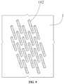
- the plurality of active areas 102 may be spaced apart from each other.
- the substrate structure of the memory may be prepared by using the method for preparing a substrate structure of a memory according to any one of the foregoing method embodiments. Therefore, the substrate structure of the memory may have the same beneficial effects which are not repeatedly described herein for the sake of conciseness.
- the memory may include the substrate structure of the memory according to the foregoing embodiments.
- the memory may further include other structures such as a capacitor structure, and this specification is not limited in this regard.
- the substrate structure included in the memory may be the same as the substrate structure in the foregoing embodiments of the substrate structure of the memory. Therefore, the substrate structure included in the memory may have the same beneficial effects as the substrate structure in the foregoing embodiments of the substrate structure of the memory, which are not repeatedly described herein for the sake of conciseness.
Landscapes
- Semiconductor Memories (AREA)
- Chemical & Material Sciences (AREA)
- Chemical Kinetics & Catalysis (AREA)
- General Chemical & Material Sciences (AREA)
- Non-Volatile Memory (AREA)
Abstract
Description
- This application claims priority to
Chinese Patent Application No.: 201911175485.7, filed on November 26, 2019 - The present invention relates to the field of integrated circuit technologies, and in particular, to a memory, a substrate structure of the memory, and a method for preparing the substrate structure of the memory.
- With the rapid development of integrated circuit technologies, memory devices are attracting more attention.
- A memory may include a substrate structure and a capacitor structure on the substrate structure. In the process of preparing the substrate structure of the memory, a plurality of strip patterns may first be formed on the substrate. Then, the strip patterns may be severed to form a mask layer, and the substrate may be etched using the mask layer as a mask to form active areas. However, the strip patterns are often difficult to be severed, making it difficult to form the active areas on the substrate.
- The information disclosed in the background part is only used to enhance the understanding of the background of the present invention, and therefore may include information that does not constitute the prior art known to a person of ordinary skill in the art.
- The purpose of the present disclosure is to provide a memory, a substrate structure of the memory and a method for preparing the substrate structure of the memory.
- One aspect of the present disclosure is directed to a method for preparing a substrate structure of a memory.
- The method includes providing a substrate; forming a first mask layer on a surface of the substrate, the first mask layer comprising a plurality of strip patterns extending in a same direction and spaced apart from each other; forming a first dielectric layer covering the first mask layer; patterning the first dielectric layer to form a plurality of sacrificial portions spaced apart from each other, the sacrificial portions covering the strip patterns; filling gaps between the sacrificial portions with a second dielectric material; forming, by removing the sacrificial portions while retaining the second dielectric material in the gaps, a second mask layer, with through-hole patterns exposing the strip patterns formed in areas that correspond to the sacrificial portions in the second mask layer; and performing layer-by-layer etching into the substrate by using the first mask layer and the second mask layer as masks to transfer the strip patterns and the through-hole patterns to form a plurality of active areas arranged in an array.
- In some embodiments of the present disclosure, patterning the first dielectric layer to form the plurality of sacrificial portions spaced apart from each other includes: forming a plurality of first through-holes distributed in an array in the first dielectric layer; and forming a plurality of second through-holes distributed in an array in the first dielectric layer.
- The first through-holes and the second through-holes may be alternately arranged in both a first direction and a second direction perpendicular to the first direction, an orthographic projection of any first through-hole on the substrate may be in contact or overlap with an orthographic projection of a neighboring second through-hole on the substrate in the first direction and the second direction. A portion of the first dielectric layer between any two neighboring first through-holes in a third direction may form the sacrificial portion, and a deviation angle of the third direction relative to the first direction may be π/4.
- In some embodiments of the present disclosure, the first through-holes and the second through-holes may have a same cross-sectional shape.
- In some embodiments of the present disclosure, the first through-holes and the second through-holes may be circular holes.
- In some embodiments of the present disclosure, the first through-holes and the second through-holes may have the same diameter.
- In some embodiments of the present disclosure, removing the sacrificial portions while retaining the second dielectric material in the gaps may include: etching the sacrificial portions to form the second mask layer, in which the through-hole patterns exposing the strip patterns are formed in the areas that correspond to the sacrificial portions in the second mask layer.
- In some embodiments of the present disclosure, an etching rate of the second dielectric material may be less than an etching rate of the sacrificial portion. Etching the sacrificial portions to form the second mask layer includes: etching the sacrificial portions and the second dielectric material to form the second mask layer, in which the through-hole patterns exposing the strip patterns are formed in the areas that correspond to the sacrificial portions in the second mask layer.
- In some embodiments of the present disclosure, the second dielectric material is silicon oxide, and a material of the sacrificial portion is silicon nitride.
- In some embodiments of the present disclosure, etching the sacrificial portions and the second dielectric material to form the second mask layer may include: etching, by using phosphoric acid, the sacrificial portions and the second dielectric material to form the second mask layer, in which the through-hole patterns exposing the strip patterns are formed in the areas that correspond to the sacrificial portions in the second mask layer.
- In some embodiments of the present disclosure, the second dielectric material is silicon nitride, and a material of the sacrificial portion is silicon oxide.
- In some embodiments of the present disclosure, etching the sacrificial portions and the second dielectric material to form the second mask layer may include: etching, by using hydrofluoric acid, the sacrificial portions and the second dielectric material to form the second mask layer, in which the through-hole patterns exposing the strip patterns are formed in the areas that correspond to the sacrificial portions in the second mask layer.
- In some embodiments of the present disclosure, performing layer-by-layer etching into the substrate by using the first mask layer and the second mask layer as masks includes: etching, using the second mask layer as a mask, the first mask layer, to transfer the through-hole patterns to the first mask layer to sever the strip patterns; and etching, using the first mask layer with severed strip patterns as a mask, the substrate, to transfer the strip patterns and the through-hole patterns to the substrate to form the plurality of active areas arranged in an array.
- In some embodiments of the present disclosure, a distance between any two adjacent sacrificial portions is greater than a maximum size of any sacrificial portion in a direction parallel to the substrate.
- In some embodiments of the present disclosure, filling the gaps between the sacrificial portions with the second dielectric material includes: forming a second dielectric layer covering the sacrificial portions and the gaps between the sacrificial portions; and removing portions of the second dielectric layer outside the gaps.
- In some embodiments of the present disclosure, removing the portions of the second dielectric layer outside the gaps includes: removing, by using a chemical mechanical polishing process, the portions of the second dielectric layer outside the gaps.
- Another aspect of the present disclosure is directed to a substrate structure of a memory. The substrate structure of the memory is prepared by any one of the methods for preparing a substrate structure of a memory described above.
- Another aspect of the present disclosure is directed to a memory. The memory includes any one of the substrate structures described above.
- According to the memory, the substrate structure of the memory, and the method for preparing the substrate structure of the memory in the present disclosure, the second mask layer is formed by removing the sacrificial portions while retaining the second dielectric material filled in the gaps between the sacrificial portions. The sacrificial portions may cover the strip patterns, so that through-holes exposing the strip patterns are formed in the areas that correspond to the sacrificial portions in the formed second mask layer. The strip patterns and the through-hole patterns can be conveniently transferred to the substrate by using the first mask layer and the second mask layer as masks to etch the substrate, so that the plurality of active areas arranged in an array can be conveniently formed.
- Other characteristics and advantages of the present disclosure will become apparent through the following detailed descriptions, or partly learned through the practice of the present invention.
- The foregoing general descriptions and the following detailed descriptions are merely examples and explanations and do not intend to limit the present invention.
- The accompanying drawings, which are incorporated into and constitute a part of the description, illustrate embodiments in accordance with the present disclosure, and are used to explain the principle of the present invention together with the description. The accompanying drawings in the following descriptions show merely some embodiments of the present invention. A person of ordinary skill in the art may still derive other accompanying drawings from these accompanying drawings without creative efforts.
-
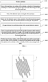
FIG. 1 is a schematic flowchart of a method for preparing a substrate structure of a memory according to an exemplary embodiment of the present disclosure. -
FIG. 2 is a schematic diagram showing a structure after step S110 of the method for preparing a substrate structure of a memory has been completed according to an exemplary embodiment of the present disclosure. -
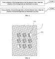
FIG. 3 is a schematic flowchart of step S130 of the method for preparing a substrate structure of a memory according to an exemplary embodiment of the present disclosure. -
FIG. 4 is a schematic diagram showing a structure after step S1301 of the method for preparing a substrate structure of a memory has been completed according to an exemplary embodiment of the present disclosure. -
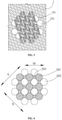
FIG. 5 is a schematic diagram showing a structure after step S1302 of the method for preparing a substrate structure of a memory has been completed according to an exemplary embodiment of the present disclosure. -
FIG. 6 is a schematic diagram of first through-holes, second through-holes, and sacrificial portions in the method for preparing a substrate structure of a memory according to an exemplary embodiment of the present disclosure. -
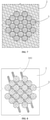
FIG. 7 is a schematic diagram showing a structure after step S140 of the method for preparing a substrate structure of a memory has been completed according to an exemplary embodiment of the present disclosure. -
FIG. 8 is a schematic diagram showing a structure after step S150 of the method for preparing a substrate structure of a memory has been completed according to an exemplary embodiment of the present disclosure. -
FIG. 9 is a schematic diagram showing a structure after step S160 of the method for preparing a substrate structure of a memory has been completed according to an exemplary embodiment of the present disclosure. - The exemplary implementations are comprehensively described with reference to the accompanying drawings. However, the example implementations can be implemented in a plurality of forms, and it should not be understood that the example implementations are limited to the example implementations described herein. On the contrary, providing these implementations makes the present invention more comprehensive and complete, and the concepts of the example implementations are comprehensively conveyed to a person skilled in the art. The described features, structures, or characteristics may be combined in one or more implementations in any proper manner. In the following descriptions, many specific details are provided to provide a full understanding of the implementations of the present invention. However, a person skilled in the art should be aware that the technical solutions in the present invention may be implemented without one or more of the specific details, or by using other methods, steps, etc. In other cases, the well-known technical solutions are not shown or described in detail in order to avoid obscuring the aspects of the present invention due to distraction.
- In addition, the accompanying drawings are merely schematic diagrams of the present invention and are not necessarily drawn to scale. Same reference signs in the figures represent same or similar parts, and therefore are not repeatedly described. Some of the block diagrams shown in the accompanying drawings are functional entities and do not necessarily correspond to physically or logically independent entities. These functional entities may be implemented in the form of software, or in one or more hardware modules or integrated circuits, or in different networks and/or processor apparatuses and/or microcontroller apparatuses.
- The terms "one", "a", and "the" are used to indicate the existence of one or more elements/components/etc. The terms "include" and "have" are used to indicate open inclusion and the existence of an element/a component/etc. in addition to the listed element/component/etc. The terms such as "first" and "second" each are merely used as a sign and constitute no limitation on the number of its object.
- This exemplary implementation first provides a method for preparing a substrate structure of a memory. Referring to
FIG. 1 , the method for preparing a substrate structure of a memory may include steps S100 through S160. - In step S100, a substrate may be provided.
- In step S110, a first mask layer may be formed on a surface of the substrate. The first mask layer may include a plurality of strip patterns extending in a same direction and spaced apart from each other.
- In step S120, a first dielectric layer covering the first mask layer may be formed.
- In step S130, the first dielectric layer may be patterned to form a plurality of sacrificial portions spaced apart from each other. The sacrificial portions may cover the strip patterns.
- In step S140, gaps between the sacrificial portions may be filled with a second dielectric material.
- In step S150, a second mask layer may be formed by removing the sacrificial portions while retaining the second dielectric material in the gaps. Through-hole patterns exposing the strip patterns may be formed in areas that correspond to the sacrificial portions in the second mask layer.
- In step S160, layer-by-layer etching, using the first mask layer and the second mask layer as masks, into the substrate may be performed. The etching may transfer the strip patterns and the through-hole patterns to the substrate to form a plurality of active areas arranged in an array.
- According to the method for preparing a substrate structure of a memory in this exemplary implementation, the second mask layer is formed by removing the sacrificial portions while retaining the second dielectric material filled in the gaps between the sacrificial portions. The sacrificial portions may cover the strip patterns, so that through-holes exposing the strip patterns may be formed in the areas that correspond to the sacrificial portions in the formed second mask layer. The strip patterns and the through-hole patterns may be conveniently transferred to the substrate by using the first mask layer and the second mask layer as masks, and the plurality of active areas arranged in an array may be formed.
- The method for preparing a substrate structure of a memory in this exemplary implementation is described below in greater details.
- In step S100, the substrate may be provided.
- The substrate may be a monocrystalline silicon substrate, a monocrystalline germanium substrate, or a silicon on insulator (SOI) substrate. The type of substrate is not specifically limited in this exemplary implementation.
- In step S110, the first mask layer may be formed on the surface of the substrate. The first mask layer may include the plurality of strip patterns extending in a same direction and spaced apart from each other.
- Referring to
FIG. 2 , the material of the first mask layer is, but not limited to, silicon oxide. In one example,strip patterns 101 may be evenly spaced apart from each other. This specification is not limited in this regard. Thestrip patterns 101 may not be evenly spaced apart from each other.
Thestrip patterns 101 may all be convex structures. In one example, forming the first mask layer on the surface of thesubstrate 1 may include: forming a first material layer on the surface of thesubstrate 1; and patterning the first material layer to form the first mask layer. The first material layer may be formed by chemical vapor deposition or atomic layer deposition. Other suitable methods may be used, and, and this specification is not limited in this regard. The patterning process may be a self-aligned dual patterning (SADP) process or a self-aligned quadruple patterning (SAQP) process. Other suitable processes may be used, and this specification is not limited in this regard. - In step S120, the first dielectric layer covering the first mask layer may be formed.
- The first dielectric layer may be prepared through chemical vapor deposition or atomic layer deposition. Other suitable methods may be used, and this specification is not limited in this regard. The first dielectric layer may be made of silicon nitride, silicon oxynitride (SiON), and silicon carbon nitride (SiCN). But the specification is not limited in this regard. The first dielectric layer may be made of silicon oxide. The thickness of the first dielectric layer is not limited in this exemplary implementation.
- In step S130, the first dielectric layer may be patterned to form the plurality of sacrificial portions spaced apart from each other. The sacrificial portions may cover the strip patterns.
- According to the present disclosure, the first dielectric layer may be patterned by using a photolithography-etching-photolithography-etching process. More specifically, referring to
FIG. 3 , patterning the first dielectric layer to form a plurality of sacrificial portions spaced apart from each other may include step S1301 and step S1302. - In step S1301, a plurality of first through-holes may be formed in the first dielectric layer. The plurality of first through-holes may be distributed in an array.
- According to the present disclosure, the plurality of first through-holes may be formed in the first dielectric layer by using a photolithography process. More specifically, the photolithography process includes: forming a photoresist layer on the first dielectric layer; exposing and developing the photoresist layer to form a plurality of channels; and etching the first dielectric layer by using the photoresist layer, in which the plurality of channels are formed, as a mask to form the first through-holes in areas that correspond to the channels in the first dielectric layer. Referring to
FIG. 4 , in some embodiments, the first through-holes 201 may be circular holes or oval holes. In some embodiments, the first through-holes 201 may be square holes, and this specification is not limited in this regard. - In step S1302, a plurality of second through-holes may be formed in the first dielectric layer. The plurality of second through-holes may be distributed in an array.
- Referring to
FIG. 5 , in some embodiments, the second through-holes 202 may be circular holes or oval holes. In some embodiments, the second through-holes 202 may be square holes, and this specification is not limited in this regard. Preferably, the second through-holes 202 and the first through-holes 201 may have the same cross-sectional shape. For example, the second through-holes 202 and the first through-holes 201 may both be circular holes. The first through-holes 201 and the second through-holes 202 may have the same size or different sizes, and this specification is not limited in this regard. - Referring to
FIGs. 5 and 6 , the first through-holes 201 and the second through-holes 202 may be alternately arranged in a first direction. That is, any first through-hole 201 may be adjacent to one second through-hole 202 in the first direction. The first direction may be the X direction. The first direction may be parallel to thesubstrate 1. Further, an orthographic projection of any first through-hole 201 on thesubstrate 1 may be in contact or overlap with an orthographic projection of a neighboring second through-hole 202 on thesubstrate 1 in the first direction. In some embodiments, the first through-holes 201 and the second through-holes 202 may be circular holes. In the first direction, an orthographic projection of any first through-hole 201 on thesubstrate 1 may be in contact or overlap with an orthographic projection of a neighboring second through-hole 202 on thesubstrate 1. That is, a distance between an axis of any first through-hole 201 and an axis of a neighboring second through-hole 202 may be less than or equal to a sum of a radius of the first through-hole 201 and a radius of the second through-hole 202. In some embodiments, the first direction may be different from an extension direction of thestrip pattern 101. - Referring to
FIGs. 5 and 6 , the first through-holes 201 and the second through-holes 202 may be alternately arranged in a second direction. That is, any first through-hole 201 may be adjacent to one second through-hole 202 in the second direction. The second direction may be the Y direction. The second direction may be parallel to thesubstrate 1 and perpendicular to the first direction. Further, an orthographic projection of any first through-hole 201 on thesubstrate 1 may be in contact or overlap with an orthographic projection of a neighboring second through-hole 202 on thesubstrate 1 in the second direction. In some embodiments, in the second direction, the first through-holes 201 and the second through-holes 202 may be circular holes. An orthographic projection of any first through-hole 201 on thesubstrate 1 may be in contact or overlap with an orthographic projection of a neighboring second through-hole 202 on thesubstrate 1. That is, a distance between an axis of any first through-hole 201 and an axis of a neighboring second through-hole 202 may be less than or equal to a sum of a radius of the first through-hole 201 and a radius of the second through-hole 202. In some embodiments, the second direction may be different from the extension direction of thestrip pattern 101. - Referring to
FIGs. 5 and 6 , a portion of the firstdielectric layer 2 between any first through-hole 201 and a neighboring first through-hole 201 in a third direction may form thesacrificial portion 203. The third direction may be the M direction. The third direction may be parallel to thesubstrate 1, and a deviation angle of the third direction relative to the first direction may be π/4. That is, an angle between the third direction and the first direction may be π/4. In some embodiments, the first through-holes 201 and the second through-holes 202 may be circular holes. Diameters of the first through-holes 201 and the second through-holes 202 may each be greater than a maximum size of thesacrificial portion 203 in a direction parallel to thesubstrate 1. In some embodiments, the third direction may be different from the extension direction of thestrip pattern 101. - In step S140, the gaps between the sacrificial portions may be filled with the second dielectric material.
- Referring to
FIGs. 6 and7 , an etching rate of the seconddielectric material 3 may be less than an etching rate of thesacrificial portion 203. The seconddielectric material 3 may be, but not limited to, BPSG (borophosphosilicate glass), BSG (borosilicate glass) or PSG (phosphosilicate glass). In some embodiments, the seconddielectric material 3 may be silicon nitride. In some embodiments, filling gaps between thesacrificial portions 203 with a seconddielectric material 3 may include: forming a second dielectric layer covering thesacrificial portions 203 and the gaps between thesacrificial portions 203; and removing portions of the second dielectric layer outside the gaps. The second dielectric layer may be formed through chemical vapor deposition or atomic layer deposition. The second dielectric layer may be formed by other suitable methods, and this specification is not limited in this regard. According to the present disclosure, the portions of the second dielectric layer outside the gaps may be removed through grinding. The grinding may be chemical mechanical polishing. In some embodiments, a portion of the firstdielectric layer 2 between any first through-hole 201 and a neighboring first through-hole 201 may form thesacrificial portion 203. The seconddielectric material 3 may be filled in the first through-holes 201 and the second through-holes 202. - In step S150, the second mask layer may be formed by removing the sacrificial portions while retaining the second dielectric material in the gaps. The through-hole patterns exposing the strip patterns may be formed in the areas that correspond to the sacrificial portions in the second mask layer.
- Referring to
FIG. 8 , the second mask layer may be formed by etching thesacrificial portions 203. Further, the second mask layer may be formed by etching thesacrificial portion 203 and the seconddielectric material 3 according to the present disclosure. The etching may be performed by using a dry etching process or a wet etching process. In some embodiments, the seconddielectric material 3 may be silicon oxide, and thesacrificial portion 203 may be made of silicon nitride. Thesacrificial portions 203 and the seconddielectric material 3 may be etched by using phosphoric acid to form the second mask layer. The through-hole patterns exposing thestrip patterns 101 may be formed in the areas that correspond to thesacrificial portions 203 in the second mask layer. In some embodiments, the seconddielectric material 3 may be silicon nitride, and the material ofsacrificial portion 203 is silicon oxide. Thesacrificial portions 203 and the seconddielectric material 3 may be etched by using hydrofluoric acid to form the second mask layer. The through-hole patterns exposing thestrip patterns 101 may be formed in the areas that correspond to thesacrificial portions 203 in the second mask layer. In some embodiments, the size of the through-hole pattern in a direction perpendicular to the extension direction of thestrip pattern 101 may be greater than the width of thestrip pattern 101. That is, the projection of the through-hole pattern on thesubstrate 1 may cover a projection of thestrip pattern 101 on thesubstrate 1. - In step S160, layer-by-layer etching into the substrate may be performed using the first mask layer and the second mask layer as masks. The etching may transfer the strip patterns and the through-hole patterns to the substrate to form the plurality of active areas arranged in an array.
- In some embodiments, performing layer-by-layer etching into the substrate by using the first mask layer and the second mask layer as masks may include: etching, using the second mask layer as a mask, the first mask layer, to transfer the through-hole patterns to the first mask layer to sever the strip patterns; and etching, using the first mask layer with severed strip patterns as a mask, the substrate, to transfer the strip patterns and the through-hole patterns to the substrate to form the plurality of active areas arranged in an array. The etching may be performed by using a dry etching process. But this specification is not limited in this regard. The etching may be a wet etching process,. In some embodiments, referring to
FIG. 9 , the plurality ofactive areas 102 may be spaced apart from each other. - This disclosure further provides a substrate structure of a memory. The substrate structure of the memory may be prepared by using the method for preparing a substrate structure of a memory according to any one of the foregoing method embodiments. Therefore, the substrate structure of the memory may have the same beneficial effects which are not repeatedly described herein for the sake of conciseness.
- This disclosure further provides a memory. The memory may include the substrate structure of the memory according to the foregoing embodiments. The memory may further include other structures such as a capacitor structure, and this specification is not limited in this regard.
- In the exemplary implementation, the substrate structure included in the memory may be the same as the substrate structure in the foregoing embodiments of the substrate structure of the memory. Therefore, the substrate structure included in the memory may have the same beneficial effects as the substrate structure in the foregoing embodiments of the substrate structure of the memory, which are not repeatedly described herein for the sake of conciseness.
- Although the steps of the method in the present invention are described in a specific order in the accompanying drawings, this does not require or imply that these steps must be performed in the specific order, or that all the shown steps must be performed to achieve the desired results. Additionally, or alternatively, some steps may be omitted, a plurality of steps may be combined into one step for execution, and/or one step is divided into a plurality of steps for execution, etc.
- A person skilled in the art can easily figure out other embodiments of the present invention after considering the specification and practicing the invention that is disclosed herein. This application is intended to cover any variations, functions, or adaptive changes of the present invention. These variations, functions, or adaptive changes comply with general principles of the present invention and include common knowledge or a commonly used technical means that is in the technical field and that is not disclosed in the present specification. The specification and the embodiments are merely considered as examples, and the actual scope and spirit of the present invention are specified by the claims.
Claims (17)
- A method for preparing a substrate structure of a memory, characterized in that, the method comprises:providing a substrate;forming a first mask layer on a surface of the substrate, a plurality of strip patterns extending in a same direction and spaced apart from each other being provided in the first mask layer;forming a first dielectric layer covering the first mask layer;patterning the first dielectric layer to form a plurality of sacrificial portions spaced apart from each other, the sacrificial portions covering the strip patterns;filling gaps between the sacrificial portions with a second dielectric material;forming, by removing the sacrificial portions while retaining the second dielectric material in the gaps, a second mask layer, with through-hole patterns exposing the strip patterns formed in areas that correspond to the sacrificial portions in the second mask layer; andperforming layer-by-layer etching into the substrate by using the first mask layer and the second mask layer as masks to transfer the strip patterns and the through-hole patterns to form a plurality of active areas arranged in an array.
- The method of preparing the substrate structure of the memory according to claim 1, wherein patterning the first dielectric layer to form the plurality of sacrificial portions spaced apart from each other comprises:forming a plurality of first through-holes distributed in an array in the first dielectric layer; andforming a plurality of second through-holes distributed in an array in the first dielectric layer, the first through-holes and the second through-holes are alternately arranged in both a first direction and a second direction perpendicular to the first direction, and an orthographic projection of any first through-hole on the substrate is in contact or overlaps with an orthographic projection of a neighboring second through-hole on the substrate in the first direction and the second direction,wherein a portion of the first dielectric layer between any two neighboring first through-holes in a third direction forms the sacrificial portions, and a deviation angle of the third direction relative to the first direction is π/4.
- The method of preparing the substrate structure of the memory according to claim 2, wherein the first through-holes and the second through-holes have a same cross-sectional shape.
- The method of preparing the substrate structure of the memory according to claim 3, wherein the first through-holes and the second through-holes are circular holes.
- The method of preparing the substrate structure of the memory according to claim 4, wherein the first through-holes and the second through-holes have a same diameter.
- The method of preparing the substrate structure of the memory according to claim 1, wherein removing the sacrificial portions while retaining the second dielectric material in the gaps comprises:
etching the sacrificial portions to form the second mask layer, wherein the through-hole patterns exposing the strip patterns are formed in the areas that correspond to the sacrificial portions in the second mask layer. - The method of preparing the substrate structure of the memory according to claim 6, wherein an etching rate of the second dielectric material is less than an etching rate of the sacrificial portion, and etching the sacrificial portions to form the second mask layer comprises:
etching the sacrificial portions and the second dielectric material to form the second mask layer, wherein the through-hole patterns exposing the strip patterns are formed in the areas that correspond to the sacrificial portions in the second mask layer. - The method of preparing the substrate structure of the memory according to claim 7, wherein the second dielectric material is silicon oxide, and a material of the sacrificial portions is silicon nitride.
- The method of preparing the substrate structure of the memory according to claim 8, wherein etching the sacrificial portions and the second dielectric material comprises:
etching, by using phosphoric acid, the sacrificial portions and the second dielectric material to form the second mask layer, wherein the through-hole patterns exposing the strip patterns are formed in the areas that correspond to the sacrificial portions in the second mask layer. - The method of preparing the substrate structure of the memory according to claim 7, wherein the second dielectric material is silicon nitride, and a material of the sacrificial portions is silicon oxide.
- The method of preparing the substrate structure of the memory according to claim 10, wherein etching the sacrificial portions and the second dielectric material to form the second mask layer comprises:
etching, by using hydrofluoric acid, the sacrificial portions and the second dielectric material to form the second mask layer, wherein the through-hole patterns exposing the strip patterns are formed in the areas that correspond to the sacrificial portions in the second mask layer. - The method of claim 1, wherein performing layer-by-layer etching into the substrate by using the first mask layer and the second mask layer as masks, comprises:etching, using the second mask layer as a mask, the first mask layer, to transfer the through-hole patterns to the first mask layer to sever the strip patterns; andetching, using the first mask layer with severed strip patterns as a mask, the substrate, to transfer the strip patterns and the through-hole patterns to the substrate to form the plurality of active areas arranged in an array.
- The method of preparing the substrate structure of the memory according to claim 1, wherein a distance between any two adjacent sacrificial portions is greater than a maximum size of any sacrificial portion in a direction parallel to the substrate.
- The method of preparing the substrate structure of the memory according to claim 1, wherein filling the gaps between the sacrificial portions with the second dielectric material comprises:forming a second dielectric layer covering the sacrificial portions and the gaps between the sacrificial portions; andremoving portions of the second dielectric layer outside the gaps.
- The method of preparing the substrate structure of the memory according to claim 14, wherein removing the portions of the second dielectric layer outside the gaps comprises:
removing, by using a chemical mechanical polishing process, the portions of the second dielectric layer outside the gaps. - A substrate structure of a memory, characterized in that, the substrate structure is prepared by a method, which comprises:providing a substrate;forming a first mask layer on a surface of the substrate, a plurality of strip patterns extending in a same direction and spaced apart from each other being provided in the first mask layer;forming a first dielectric layer covering the first mask layer;patterning the first dielectric layer to form a plurality of sacrificial portions spaced apart from each other, the sacrificial portions covering the strip patterns;filling gaps between the sacrificial portions with a second dielectric material;forming, by removing the sacrificial portions while retaining the second dielectric material in the gaps, a second mask layer, with through-hole patterns exposing the strip patterns formed in areas that correspond to the sacrificial portions in the second mask layer; andperforming layer-by-layer etching into the substrate by using the first mask layer and the second mask layer as masks to transfer the strip patterns and the through-hole patterns to form a plurality of active areas arranged in an array.
- A memory, characterized in that, the memory comprises the substrate structure of claim 16.
Applications Claiming Priority (2)
| Application Number | Priority Date | Filing Date | Title |
|---|---|---|---|
| CN201911175485.7A CN112864152B (en) | 2019-11-26 | 2019-11-26 | Memory, substrate structure of memory and preparation method of substrate structure |
| PCT/CN2020/099985 WO2021103535A1 (en) | 2019-11-26 | 2020-07-02 | Memory, memory substrate structure, and preparation method for memory substrate structure |
Publications (3)
| Publication Number | Publication Date |
|---|---|
| EP3971974A1 true EP3971974A1 (en) | 2022-03-23 |
| EP3971974A4 EP3971974A4 (en) | 2022-09-28 |
| EP3971974B1 EP3971974B1 (en) | 2023-10-25 |
Family
ID=75985838
Family Applications (1)
| Application Number | Title | Priority Date | Filing Date |
|---|---|---|---|
| EP20891550.4A Active EP3971974B1 (en) | 2019-11-26 | 2020-07-02 | Memory, memory substrate structure, and preparation method for memory substrate structure |
Country Status (4)
| Country | Link |
|---|---|
| US (1) | US12014932B2 (en) |
| EP (1) | EP3971974B1 (en) |
| CN (1) | CN112864152B (en) |
| WO (1) | WO2021103535A1 (en) |
Families Citing this family (1)
| Publication number | Priority date | Publication date | Assignee | Title |
|---|---|---|---|---|
| CN115000293A (en) * | 2022-05-25 | 2022-09-02 | 长鑫存储技术有限公司 | Preparation method of semiconductor structure, semiconductor structure and memory |
Family Cites Families (14)
| Publication number | Priority date | Publication date | Assignee | Title |
|---|---|---|---|---|
| KR20110112723A (en) * | 2010-04-07 | 2011-10-13 | 주식회사 하이닉스반도체 | Cutting mask for active formation of diagonal structures |
| KR20120075037A (en) * | 2010-12-28 | 2012-07-06 | 삼성전자주식회사 | Method of manufacturing semiconductor device |
| CN105244321B (en) * | 2014-06-17 | 2018-12-21 | 中芯国际集成电路制造(上海)有限公司 | A kind of semiconductor devices and its manufacturing method and electronic device |
| US9324619B2 (en) | 2014-08-25 | 2016-04-26 | Samsung Electronics Co., Ltd. | Semiconductor device and method of fabricating the same |
| US9773838B2 (en) * | 2014-09-04 | 2017-09-26 | Toshiba Memory Corporation | Magnetoresistive memory device and manufacturing method of the same |
| KR20160085043A (en) * | 2015-01-07 | 2016-07-15 | 에스케이하이닉스 주식회사 | Method for fabricating pattern |
| KR102265271B1 (en) * | 2015-01-14 | 2021-06-17 | 삼성전자주식회사 | Semiconductor devices and method for forming the same |
| KR102280471B1 (en) * | 2015-07-20 | 2021-07-22 | 삼성전자주식회사 | Method of forming active patterns, active pattern array, and method of manufacturing semiconductor device |
| KR102367493B1 (en) * | 2017-03-06 | 2022-02-24 | 삼성전자주식회사 | Semiconductor devices and methods of manufacturing the same |
| CN109148376B (en) * | 2017-06-28 | 2020-07-31 | 长鑫存储技术有限公司 | Memory and forming method thereof, and semiconductor device |
| US10290681B2 (en) * | 2017-09-21 | 2019-05-14 | Sandisk Technologies Llc | Array of hole-type surround gate vertical field effect transistors and method of making thereof |
| CN107706206A (en) * | 2017-11-02 | 2018-02-16 | 睿力集成电路有限公司 | Array of capacitors and forming method thereof, semiconductor devices |
| CN110021518B (en) * | 2018-01-09 | 2020-12-22 | 联华电子股份有限公司 | Self-aligned double patterning method |
| US11342333B2 (en) * | 2019-09-26 | 2022-05-24 | Nanya Technology Corporation | Semiconductor device |
-
2019
- 2019-11-26 CN CN201911175485.7A patent/CN112864152B/en active Active
-
2020
- 2020-07-02 EP EP20891550.4A patent/EP3971974B1/en active Active
- 2020-07-02 WO PCT/CN2020/099985 patent/WO2021103535A1/en not_active Ceased
-
2021
- 2021-08-07 US US17/396,690 patent/US12014932B2/en active Active
Also Published As
| Publication number | Publication date |
|---|---|
| CN112864152A (en) | 2021-05-28 |
| WO2021103535A1 (en) | 2021-06-03 |
| US12014932B2 (en) | 2024-06-18 |
| EP3971974A4 (en) | 2022-09-28 |
| EP3971974B1 (en) | 2023-10-25 |
| CN112864152B (en) | 2022-06-24 |
| US20210366725A1 (en) | 2021-11-25 |
Similar Documents
| Publication | Publication Date | Title |
|---|---|---|
| JP4996155B2 (en) | Semiconductor device and manufacturing method thereof | |
| CN108931882B (en) | Semiconductor device with a plurality of transistors | |
| CN113675146A (en) | Semiconductor structure, method of forming the same, and memory | |
| KR102720606B1 (en) | Method for fabricating semiconductor device | |
| CN109148269B (en) | Method of forming semiconductor device | |
| CN115548086B (en) | Semiconductor device fabrication methods | |
| EP3971974B1 (en) | Memory, memory substrate structure, and preparation method for memory substrate structure | |
| KR20160125830A (en) | Methods of manufacturing semiconductor devices | |
| CN112447513A (en) | Semiconductor structure and forming method thereof | |
| CN111668093A (en) | Semiconductor device and method of forming the same | |
| EP3097581B1 (en) | Double patterning method of forming semiconductor active areas and isolation regions | |
| EP4207287B1 (en) | Semiconductor device, semiconductor structure and forming method therefor | |
| CN113506728B (en) | Method for manufacturing semiconductor structure and semiconductor structure | |
| EP3840034B1 (en) | Method for producing nanoscaled electrically conductive lines for semiconductor devices | |
| KR100237751B1 (en) | Manufacturing method of semiconductor memory device | |
| CN114446884B (en) | Semiconductor structure and method for forming the same | |
| KR20140028722A (en) | Method for manufacturing hole pattern in semiconductor device | |
| US20140252556A1 (en) | Single-mask spacer technique for semiconductor device features | |
| CN111863705B (en) | Method for forming isolation of semiconductor device | |
| WO2024036718A1 (en) | Semiconductor structure and method for forming same | |
| CN111564408B (en) | A method of forming an opening | |
| KR20010056936A (en) | Method for forming fine contact hole in semiconductor device | |
| KR100271786B1 (en) | Method for forming capacitor electrode of semiconductor device | |
| WO2023221311A1 (en) | Semiconductor structure and forming method therefor | |
| JP3277807B2 (en) | Semiconductor device and manufacturing method thereof |
Legal Events
| Date | Code | Title | Description |
|---|---|---|---|
| STAA | Information on the status of an ep patent application or granted ep patent |
Free format text: STATUS: THE INTERNATIONAL PUBLICATION HAS BEEN MADE |
|
| PUAI | Public reference made under article 153(3) epc to a published international application that has entered the european phase |
Free format text: ORIGINAL CODE: 0009012 |
|
| STAA | Information on the status of an ep patent application or granted ep patent |
Free format text: STATUS: REQUEST FOR EXAMINATION WAS MADE |
|
| 17P | Request for examination filed |
Effective date: 20211215 |
|
| AK | Designated contracting states |
Kind code of ref document: A1 Designated state(s): AL AT BE BG CH CY CZ DE DK EE ES FI FR GB GR HR HU IE IS IT LI LT LU LV MC MK MT NL NO PL PT RO RS SE SI SK SM TR |
|
| A4 | Supplementary search report drawn up and despatched |
Effective date: 20220825 |
|
| RIC1 | Information provided on ipc code assigned before grant |
Ipc: H01L 21/308 20060101ALI20220819BHEP Ipc: H01L 27/108 20060101AFI20220819BHEP |
|
| DAV | Request for validation of the european patent (deleted) | ||
| DAX | Request for extension of the european patent (deleted) | ||
| REG | Reference to a national code |
Ref country code: DE Ref legal event code: R079 Free format text: PREVIOUS MAIN CLASS: H01L0027108000 Ipc: H01L0021308000 Ref document number: 602020020030 Country of ref document: DE |
|
| GRAP | Despatch of communication of intention to grant a patent |
Free format text: ORIGINAL CODE: EPIDOSNIGR1 |
|
| STAA | Information on the status of an ep patent application or granted ep patent |
Free format text: STATUS: GRANT OF PATENT IS INTENDED |
|
| RIC1 | Information provided on ipc code assigned before grant |
Ipc: H10B 12/00 20230101ALI20230424BHEP Ipc: H01L 21/308 20060101AFI20230424BHEP |
|
| INTG | Intention to grant announced |
Effective date: 20230519 |
|
| GRAS | Grant fee paid |
Free format text: ORIGINAL CODE: EPIDOSNIGR3 |
|
| GRAA | (expected) grant |
Free format text: ORIGINAL CODE: 0009210 |
|
| STAA | Information on the status of an ep patent application or granted ep patent |
Free format text: STATUS: THE PATENT HAS BEEN GRANTED |
|
| P01 | Opt-out of the competence of the unified patent court (upc) registered |
Effective date: 20230822 |
|
| AK | Designated contracting states |
Kind code of ref document: B1 Designated state(s): AL AT BE BG CH CY CZ DE DK EE ES FI FR GB GR HR HU IE IS IT LI LT LU LV MC MK MT NL NO PL PT RO RS SE SI SK SM TR |
|
| REG | Reference to a national code |
Ref country code: GB Ref legal event code: FG4D |
|
| REG | Reference to a national code |
Ref country code: CH Ref legal event code: EP |
|
| REG | Reference to a national code |
Ref country code: DE Ref legal event code: R096 Ref document number: 602020020030 Country of ref document: DE |
|
| REG | Reference to a national code |
Ref country code: IE Ref legal event code: FG4D |
|
| REG | Reference to a national code |
Ref country code: LT Ref legal event code: MG9D |
|
| REG | Reference to a national code |
Ref country code: NL Ref legal event code: MP Effective date: 20231025 |
|
| REG | Reference to a national code |
Ref country code: AT Ref legal event code: MK05 Ref document number: 1625565 Country of ref document: AT Kind code of ref document: T Effective date: 20231025 |
|
| PG25 | Lapsed in a contracting state [announced via postgrant information from national office to epo] |
Ref country code: NL Free format text: LAPSE BECAUSE OF FAILURE TO SUBMIT A TRANSLATION OF THE DESCRIPTION OR TO PAY THE FEE WITHIN THE PRESCRIBED TIME-LIMIT Effective date: 20231025 |
|
| PG25 | Lapsed in a contracting state [announced via postgrant information from national office to epo] |
Ref country code: GR Free format text: LAPSE BECAUSE OF FAILURE TO SUBMIT A TRANSLATION OF THE DESCRIPTION OR TO PAY THE FEE WITHIN THE PRESCRIBED TIME-LIMIT Effective date: 20240126 |
|
| PG25 | Lapsed in a contracting state [announced via postgrant information from national office to epo] |
Ref country code: IS Free format text: LAPSE BECAUSE OF FAILURE TO SUBMIT A TRANSLATION OF THE DESCRIPTION OR TO PAY THE FEE WITHIN THE PRESCRIBED TIME-LIMIT Effective date: 20240225 |
|
| PG25 | Lapsed in a contracting state [announced via postgrant information from national office to epo] |
Ref country code: LT Free format text: LAPSE BECAUSE OF FAILURE TO SUBMIT A TRANSLATION OF THE DESCRIPTION OR TO PAY THE FEE WITHIN THE PRESCRIBED TIME-LIMIT Effective date: 20231025 |
|
| PG25 | Lapsed in a contracting state [announced via postgrant information from national office to epo] |
Ref country code: AT Free format text: LAPSE BECAUSE OF FAILURE TO SUBMIT A TRANSLATION OF THE DESCRIPTION OR TO PAY THE FEE WITHIN THE PRESCRIBED TIME-LIMIT Effective date: 20231025 |
|
| PG25 | Lapsed in a contracting state [announced via postgrant information from national office to epo] |
Ref country code: ES Free format text: LAPSE BECAUSE OF FAILURE TO SUBMIT A TRANSLATION OF THE DESCRIPTION OR TO PAY THE FEE WITHIN THE PRESCRIBED TIME-LIMIT Effective date: 20231025 |
|
| PG25 | Lapsed in a contracting state [announced via postgrant information from national office to epo] |
Ref country code: LT Free format text: LAPSE BECAUSE OF FAILURE TO SUBMIT A TRANSLATION OF THE DESCRIPTION OR TO PAY THE FEE WITHIN THE PRESCRIBED TIME-LIMIT Effective date: 20231025 Ref country code: IS Free format text: LAPSE BECAUSE OF FAILURE TO SUBMIT A TRANSLATION OF THE DESCRIPTION OR TO PAY THE FEE WITHIN THE PRESCRIBED TIME-LIMIT Effective date: 20240225 Ref country code: GR Free format text: LAPSE BECAUSE OF FAILURE TO SUBMIT A TRANSLATION OF THE DESCRIPTION OR TO PAY THE FEE WITHIN THE PRESCRIBED TIME-LIMIT Effective date: 20240126 Ref country code: ES Free format text: LAPSE BECAUSE OF FAILURE TO SUBMIT A TRANSLATION OF THE DESCRIPTION OR TO PAY THE FEE WITHIN THE PRESCRIBED TIME-LIMIT Effective date: 20231025 Ref country code: BG Free format text: LAPSE BECAUSE OF FAILURE TO SUBMIT A TRANSLATION OF THE DESCRIPTION OR TO PAY THE FEE WITHIN THE PRESCRIBED TIME-LIMIT Effective date: 20240125 Ref country code: AT Free format text: LAPSE BECAUSE OF FAILURE TO SUBMIT A TRANSLATION OF THE DESCRIPTION OR TO PAY THE FEE WITHIN THE PRESCRIBED TIME-LIMIT Effective date: 20231025 Ref country code: PT Free format text: LAPSE BECAUSE OF FAILURE TO SUBMIT A TRANSLATION OF THE DESCRIPTION OR TO PAY THE FEE WITHIN THE PRESCRIBED TIME-LIMIT Effective date: 20240226 |
|
| PG25 | Lapsed in a contracting state [announced via postgrant information from national office to epo] |
Ref country code: SE Free format text: LAPSE BECAUSE OF FAILURE TO SUBMIT A TRANSLATION OF THE DESCRIPTION OR TO PAY THE FEE WITHIN THE PRESCRIBED TIME-LIMIT Effective date: 20231025 Ref country code: RS Free format text: LAPSE BECAUSE OF FAILURE TO SUBMIT A TRANSLATION OF THE DESCRIPTION OR TO PAY THE FEE WITHIN THE PRESCRIBED TIME-LIMIT Effective date: 20231025 Ref country code: PL Free format text: LAPSE BECAUSE OF FAILURE TO SUBMIT A TRANSLATION OF THE DESCRIPTION OR TO PAY THE FEE WITHIN THE PRESCRIBED TIME-LIMIT Effective date: 20231025 Ref country code: NO Free format text: LAPSE BECAUSE OF FAILURE TO SUBMIT A TRANSLATION OF THE DESCRIPTION OR TO PAY THE FEE WITHIN THE PRESCRIBED TIME-LIMIT Effective date: 20240125 Ref country code: LV Free format text: LAPSE BECAUSE OF FAILURE TO SUBMIT A TRANSLATION OF THE DESCRIPTION OR TO PAY THE FEE WITHIN THE PRESCRIBED TIME-LIMIT Effective date: 20231025 Ref country code: HR Free format text: LAPSE BECAUSE OF FAILURE TO SUBMIT A TRANSLATION OF THE DESCRIPTION OR TO PAY THE FEE WITHIN THE PRESCRIBED TIME-LIMIT Effective date: 20231025 |
|
| PG25 | Lapsed in a contracting state [announced via postgrant information from national office to epo] |
Ref country code: DK Free format text: LAPSE BECAUSE OF FAILURE TO SUBMIT A TRANSLATION OF THE DESCRIPTION OR TO PAY THE FEE WITHIN THE PRESCRIBED TIME-LIMIT Effective date: 20231025 |
|
| PG25 | Lapsed in a contracting state [announced via postgrant information from national office to epo] |
Ref country code: CZ Free format text: LAPSE BECAUSE OF FAILURE TO SUBMIT A TRANSLATION OF THE DESCRIPTION OR TO PAY THE FEE WITHIN THE PRESCRIBED TIME-LIMIT Effective date: 20231025 |
|
| REG | Reference to a national code |
Ref country code: DE Ref legal event code: R097 Ref document number: 602020020030 Country of ref document: DE |
|
| PG25 | Lapsed in a contracting state [announced via postgrant information from national office to epo] |
Ref country code: SK Free format text: LAPSE BECAUSE OF FAILURE TO SUBMIT A TRANSLATION OF THE DESCRIPTION OR TO PAY THE FEE WITHIN THE PRESCRIBED TIME-LIMIT Effective date: 20231025 |
|
| PG25 | Lapsed in a contracting state [announced via postgrant information from national office to epo] |
Ref country code: SM Free format text: LAPSE BECAUSE OF FAILURE TO SUBMIT A TRANSLATION OF THE DESCRIPTION OR TO PAY THE FEE WITHIN THE PRESCRIBED TIME-LIMIT Effective date: 20231025 Ref country code: SK Free format text: LAPSE BECAUSE OF FAILURE TO SUBMIT A TRANSLATION OF THE DESCRIPTION OR TO PAY THE FEE WITHIN THE PRESCRIBED TIME-LIMIT Effective date: 20231025 Ref country code: RO Free format text: LAPSE BECAUSE OF FAILURE TO SUBMIT A TRANSLATION OF THE DESCRIPTION OR TO PAY THE FEE WITHIN THE PRESCRIBED TIME-LIMIT Effective date: 20231025 Ref country code: IT Free format text: LAPSE BECAUSE OF FAILURE TO SUBMIT A TRANSLATION OF THE DESCRIPTION OR TO PAY THE FEE WITHIN THE PRESCRIBED TIME-LIMIT Effective date: 20231025 Ref country code: EE Free format text: LAPSE BECAUSE OF FAILURE TO SUBMIT A TRANSLATION OF THE DESCRIPTION OR TO PAY THE FEE WITHIN THE PRESCRIBED TIME-LIMIT Effective date: 20231025 Ref country code: DK Free format text: LAPSE BECAUSE OF FAILURE TO SUBMIT A TRANSLATION OF THE DESCRIPTION OR TO PAY THE FEE WITHIN THE PRESCRIBED TIME-LIMIT Effective date: 20231025 Ref country code: CZ Free format text: LAPSE BECAUSE OF FAILURE TO SUBMIT A TRANSLATION OF THE DESCRIPTION OR TO PAY THE FEE WITHIN THE PRESCRIBED TIME-LIMIT Effective date: 20231025 |
|
| PLBE | No opposition filed within time limit |
Free format text: ORIGINAL CODE: 0009261 |
|
| STAA | Information on the status of an ep patent application or granted ep patent |
Free format text: STATUS: NO OPPOSITION FILED WITHIN TIME LIMIT |
|
| 26N | No opposition filed |
Effective date: 20240726 |
|
| PG25 | Lapsed in a contracting state [announced via postgrant information from national office to epo] |
Ref country code: SI Free format text: LAPSE BECAUSE OF FAILURE TO SUBMIT A TRANSLATION OF THE DESCRIPTION OR TO PAY THE FEE WITHIN THE PRESCRIBED TIME-LIMIT Effective date: 20231025 |
|
| PG25 | Lapsed in a contracting state [announced via postgrant information from national office to epo] |
Ref country code: SI Free format text: LAPSE BECAUSE OF FAILURE TO SUBMIT A TRANSLATION OF THE DESCRIPTION OR TO PAY THE FEE WITHIN THE PRESCRIBED TIME-LIMIT Effective date: 20231025 |
|
| PG25 | Lapsed in a contracting state [announced via postgrant information from national office to epo] |
Ref country code: MC Free format text: LAPSE BECAUSE OF FAILURE TO SUBMIT A TRANSLATION OF THE DESCRIPTION OR TO PAY THE FEE WITHIN THE PRESCRIBED TIME-LIMIT Effective date: 20231025 |
|
| REG | Reference to a national code |
Ref country code: CH Ref legal event code: PL |
|
| PG25 | Lapsed in a contracting state [announced via postgrant information from national office to epo] |
Ref country code: LU Free format text: LAPSE BECAUSE OF NON-PAYMENT OF DUE FEES Effective date: 20240702 |
|
| PG25 | Lapsed in a contracting state [announced via postgrant information from national office to epo] |
Ref country code: LU Free format text: LAPSE BECAUSE OF NON-PAYMENT OF DUE FEES Effective date: 20240702 |
|
| PG25 | Lapsed in a contracting state [announced via postgrant information from national office to epo] |
Ref country code: CH Free format text: LAPSE BECAUSE OF NON-PAYMENT OF DUE FEES Effective date: 20240731 Ref country code: BE Free format text: LAPSE BECAUSE OF NON-PAYMENT OF DUE FEES Effective date: 20240731 |
|
| REG | Reference to a national code |
Ref country code: BE Ref legal event code: MM Effective date: 20240731 |
|
| PG25 | Lapsed in a contracting state [announced via postgrant information from national office to epo] |
Ref country code: IE Free format text: LAPSE BECAUSE OF NON-PAYMENT OF DUE FEES Effective date: 20240702 |
|
| PG25 | Lapsed in a contracting state [announced via postgrant information from national office to epo] |
Ref country code: FI Free format text: LAPSE BECAUSE OF FAILURE TO SUBMIT A TRANSLATION OF THE DESCRIPTION OR TO PAY THE FEE WITHIN THE PRESCRIBED TIME-LIMIT Effective date: 20231025 |
|
| PGFP | Annual fee paid to national office [announced via postgrant information from national office to epo] |
Ref country code: DE Payment date: 20250722 Year of fee payment: 6 |
|
| PGFP | Annual fee paid to national office [announced via postgrant information from national office to epo] |
Ref country code: GB Payment date: 20250722 Year of fee payment: 6 |
|
| PGFP | Annual fee paid to national office [announced via postgrant information from national office to epo] |
Ref country code: FR Payment date: 20250725 Year of fee payment: 6 |
|
| PG25 | Lapsed in a contracting state [announced via postgrant information from national office to epo] |
Ref country code: CY Free format text: LAPSE BECAUSE OF FAILURE TO SUBMIT A TRANSLATION OF THE DESCRIPTION OR TO PAY THE FEE WITHIN THE PRESCRIBED TIME-LIMIT; INVALID AB INITIO Effective date: 20200702 |
|
| REG | Reference to a national code |
Ref country code: DE Ref legal event code: R079 Ref document number: 602020020030 Country of ref document: DE Free format text: PREVIOUS MAIN CLASS: H01L0021308000 Ipc: H10P0050000000 |
|
| PG25 | Lapsed in a contracting state [announced via postgrant information from national office to epo] |
Ref country code: HU Free format text: LAPSE BECAUSE OF FAILURE TO SUBMIT A TRANSLATION OF THE DESCRIPTION OR TO PAY THE FEE WITHIN THE PRESCRIBED TIME-LIMIT; INVALID AB INITIO Effective date: 20200702 |