EP3950274B1 - Verfahren zur herstellung eines gehäuses einer energiesammelvorrichtung - Google Patents
Verfahren zur herstellung eines gehäuses einer energiesammelvorrichtung Download PDFInfo
- Publication number
- EP3950274B1 EP3950274B1 EP21185894.9A EP21185894A EP3950274B1 EP 3950274 B1 EP3950274 B1 EP 3950274B1 EP 21185894 A EP21185894 A EP 21185894A EP 3950274 B1 EP3950274 B1 EP 3950274B1
- Authority
- EP
- European Patent Office
- Prior art keywords
- housing
- construction
- layer construction
- comb structures
- producing
- Prior art date
- Legal status (The legal status is an assumption and is not a legal conclusion. Google has not performed a legal analysis and makes no representation as to the accuracy of the status listed.)
- Active
Links
Images


Classifications
-
- B—PERFORMING OPERATIONS; TRANSPORTING
- B29—WORKING OF PLASTICS; WORKING OF SUBSTANCES IN A PLASTIC STATE IN GENERAL
- B29C—SHAPING OR JOINING OF PLASTICS; SHAPING OF MATERIAL IN A PLASTIC STATE, NOT OTHERWISE PROVIDED FOR; AFTER-TREATMENT OF THE SHAPED PRODUCTS, e.g. REPAIRING
- B29C64/00—Additive manufacturing, i.e. manufacturing of three-dimensional [3D] objects by additive deposition, additive agglomeration or additive layering, e.g. by 3D printing, stereolithography or selective laser sintering
- B29C64/10—Processes of additive manufacturing
- B29C64/106—Processes of additive manufacturing using only liquids or viscous materials, e.g. depositing a continuous bead of viscous material
- B29C64/112—Processes of additive manufacturing using only liquids or viscous materials, e.g. depositing a continuous bead of viscous material using individual droplets, e.g. from jetting heads
-
- B—PERFORMING OPERATIONS; TRANSPORTING
- B29—WORKING OF PLASTICS; WORKING OF SUBSTANCES IN A PLASTIC STATE IN GENERAL
- B29C—SHAPING OR JOINING OF PLASTICS; SHAPING OF MATERIAL IN A PLASTIC STATE, NOT OTHERWISE PROVIDED FOR; AFTER-TREATMENT OF THE SHAPED PRODUCTS, e.g. REPAIRING
- B29C64/00—Additive manufacturing, i.e. manufacturing of three-dimensional [3D] objects by additive deposition, additive agglomeration or additive layering, e.g. by 3D printing, stereolithography or selective laser sintering
- B29C64/10—Processes of additive manufacturing
- B29C64/106—Processes of additive manufacturing using only liquids or viscous materials, e.g. depositing a continuous bead of viscous material
-
- B—PERFORMING OPERATIONS; TRANSPORTING
- B33—ADDITIVE MANUFACTURING TECHNOLOGY
- B33Y—ADDITIVE MANUFACTURING, i.e. MANUFACTURING OF THREE-DIMENSIONAL [3D] OBJECTS BY ADDITIVE DEPOSITION, ADDITIVE AGGLOMERATION OR ADDITIVE LAYERING, e.g. BY 3D PRINTING, STEREOLITHOGRAPHY OR SELECTIVE LASER SINTERING
- B33Y10/00—Processes of additive manufacturing
-
- B—PERFORMING OPERATIONS; TRANSPORTING
- B33—ADDITIVE MANUFACTURING TECHNOLOGY
- B33Y—ADDITIVE MANUFACTURING, i.e. MANUFACTURING OF THREE-DIMENSIONAL [3D] OBJECTS BY ADDITIVE DEPOSITION, ADDITIVE AGGLOMERATION OR ADDITIVE LAYERING, e.g. BY 3D PRINTING, STEREOLITHOGRAPHY OR SELECTIVE LASER SINTERING
- B33Y80/00—Products made by additive manufacturing
Definitions
- the invention relates to a method for producing a housing of an energy collection device by means of an additive manufacturing method, such as the 3D printing method, in particular 3D dispensing. Furthermore, the invention relates to the use of the method for producing housings, for example for energy-autonomous sensor systems.
- EP 2 078 312 B1 has as its subject an energy collection device manufactured by means of a print forming process.
- the device comprises a housing comprising a bottom portion with a peripheral wall portion, which are integrally formed by building up a rim in the periphery of the bottom portion, wherein the bottom portion comprises one or more holes to allow the drainage of sacrificial material during a print forming process used during the manufacture of the device.
- a piezoelectric cantilever beam is provided, which is integrally formed as part of the peripheral wall portion and protrudes beyond a region of the bottom portion, wherein the piezoelectric cantilever beam has a first electrode layer, a ceramic layer arranged on the first electrode layer, and a second electrode layer arranged on the ceramic layer.
- a first passage is provided, which is formed within the peripheral wall portion and is coupled to the first electrode layer. Furthermore, a second passage is provided, which is formed within the peripheral wall portion and is coupled to the second electrode layer.
- An additional mass is connected to the piezoelectric cantilever beam.
- a cavity separates the cantilever beam from the bottom portion, the cavity configured to allow at least one end of the cantilever beam to move vertically relative to the bottom portion in response to a moving device, the cavity being created when sacrificial material drains through the holes during the print forming process.
- a lid is provided disposed on an upper region of the edge wall portion of the housing to seal the piezoelectric cantilever beam within the cavity.
- a first surface mount pad is coupled to the first passageway on a surface of the lid, a second surface mount pad on the surface of the lid is coupled to the second passageway.
- US 2018/120912 A1 refers to a manufacturing method of a thermal management device including its housing, which is mainly based on an additive manufacturing process.
- US 2014/333011 A1 relates to an additive manufacturing process in which a wall structure is produced on a print bed.
- a support piece with a non-stick surface is placed near or within the structure, a layer of material is additively manufactured on one or more walls and on the support piece to create a protrusion, and the support piece is removed again after the material forming the protrusion has returned to a solid state or hardened.
- WO 2019/147 700 A1 deals with an additive manufacturing process.
- US 2019/0110366 A1 relates to a method for producing a component carrier, wherein at least a part of the component carrier is formed as a three-dimensional structure.
- the solution proposed according to the invention can provide a housing of an energy collection device by additive manufacturing, which has a high degree of functionalization.
- the high degree of functionalization can be brought about in particular by a plastic-based extrusion process, wherein the functionalization can be achieved in a manufacturing process.
- the method proposed according to the invention advantageously allows a material, in particular a cationically polymerizable epoxy resin, to be used as a construction material.
- This material can be used to specifically adjust the material properties of the resulting housing so that the housing can perform several functions. These include, for example, providing a supporting structure with defined rigidity and damping, ensuring that a comb structure is clamped using, for example, a positive connection, and thermally insulating the energy collection and electronic levels.
- the building material is presented as a dual-crosslinked material, in particular a material that can be chemically pre-crosslinked by a UV radiation source.
- a total thermal cross-linking is carried out, so that in particular the components of a multi-part housing experience a total cross-linking and thus mechanical stability on the one hand and encapsulation against environmental influences on the other hand can be ensured.
- the housing manufactured in the additive layer structure has a defined stiffness and a defined damping and is designed in a load-bearing structural design.
- thermal insulation of the comb structures and/or the circuit board and its electronic components is ensured within the housing.
- a material-locking connection is produced by bonding the comb structures to the UV-crosslinked layers with uncrosslinked dispenser material, in particular wet layers.
- the additive layer structure created by the method proposed according to the invention is provided with assembly aids during the manufacture of the housing, in particular in the base area thereof, which serve to fix structures and/or circuit boards to be inserted.
- the assembly aids are supports so that, for example, bending beams do not bend into a cavity below.
- adhesive trays are produced within the clamping areas, which have a geometry that particularly reduces stress concentration peaks.
- Such a geometry of adhesive trays allows mechanical load peaks that would have to be absorbed by the housing to be significantly reduced, so that a long service life can be achieved.
- the invention relates to the use of the method for producing housings for energy-autonomous sensor systems.
- the solution proposed according to the invention makes it possible to provide a housing production system, whereby functional integration can be achieved during the manufacture of the housing, preferably in an additive manufacturing process, in particular 3D dispensing.
- Comb structures with additional masses and a circuit board equipped with electronic components that enables power management can be embedded and fixed in one spatial direction in the housing during its construction in a manufacturing process between the individual printing sections of the 3D dispensing.
- the material properties of the housing produced according to the invention can be specifically adjusted.
- the housing produced can take on several functions, including the provision of a supporting structure with a defined rigidity and a predetermined, defined damping behavior.
- the housing proposed according to the invention is designed in such a way that the clamping or clamping of the comb structures is ensured, for example by means of a positive connection within the housing.
- the manufacturing process proposed according to the invention can be used to achieve thermal insulation of an energy collection level and a circuit board level.
- the construction material can be used as an adhesive through incomplete chemical cross-linking. Material-locking connections can be created by gluing the comb structures to the printed housing with non-pre-cross-linked dispensing material. This results in the advantage that the clamping area is relieved by minimizing the notch stress directly through the additive construction without complex design of the clamping device or complex planning of force curves.
- the solution proposed by the invention also allows a relatively high product variance to be achieved due to the flexible adaptation of the housing to various mechanical interfaces. Examples include Christmas tree clips, inserts, holes and the like.
- 3D dispensing the advantages of this additive manufacturing technology, ie a quick change of geometry without complex tool adjustment, can be used in a significant way.
- Assembly aids formed in the base area of the additively manufactured housing as well as the first layers of the wall or clamping areas for the components to be fitted simultaneously provide assembly aids for the lowest energy collection level that is then to be inserted.
- separate positioning aids can advantageously be dispensed with.
- a process representation of 3D dispensing can be seen in the illustration according to the sequence of figures 1.1 to 1.5.
- a three-dimensional model is divided into individual, quasi two-dimensional layers in preparation for 3D dispensing production.
- a first constructed object 10 is additively built up layer by layer using 3D dispensing.
- the individual layers 12 are moved through a dispenser head according to their geometry and filled with the appropriate building material. After an individual layer 12 has been built up, it is chemically pre-crosslinked using a UV radiation source 14.
- Figure 1.2 shows a second constructed object 16, which is constructed by individual layers 12 in the vertical direction, wherein each individual layer 12 is irradiated via a UV radiation source 14 for chemical pre-crosslinking.
- FIG. 1.3 shows, for example, a box-shaped first constructed object 10, which is constructed from individual layers 12. A cavity is created according to the length of the individual layers 12. A wet layer 20 of construction material is applied to a contact surface 18. Then, as in Figure 1.4 As shown, a second constructed object 16 is applied to the contact surfaces 18 coated with the wet layer 20. The second constructed object 16 is gripped by a conveying tool 22 and applied to the contact surfaces 18.
- FIG. 2 shows an isometric view of a shell-like housing of an energy collector.
- a housing 30 which can comprise a profile groove 32, is provided with a first layer 34, an overlying second layer 36 and a third layer 38 in the Z direction 40.
- the respective layers 34, 36, 38 are clamped 42 using individual spacers 44.
- the wall of the housing 30 as shown in Figure 2 is provided with a standard plug 46.
- the standard plug 46 represents an additively created breakthrough or an opening in the housing 30, which forms a potential weak point for the wall of the housing 30.
- the first layer 34 and the second layer 36 are each provided with a number of additional masses 48.
- the housing 30 also has a mounting option 50 for a vibration source.
- FIG. 3.1 The figure sequence of the Figures 3.1, 3.2 and 3.3 different variants of clamping areas 58 can be seen, by means of which individual collecting structures 56 are contained in a housing 30, which is built up by an additive layer structure 64 in the Z direction 40, for example.
- a collecting structure 56 is fixed between UV-pre-crosslinked planes 60 in the clamping area 58 of the additive layer structure 64 shown there.
- the collecting structure 56 is, for example, a bending beam 68 or the like.
- the additive layer structure 64 is carried out in the Z direction (see position 40).
- An X direction 52 extends perpendicular to this. From the drawing plane according to the Figure 3.1 protrudes a Y-direction 54.
- the end of the collecting structure 56 which is formed by a wet layer 62 of non-crosslinked construction material, is cast and fixed in the clamping area 58.
- the additive layer build-up 64 takes place in the Z direction 40 in the beam thickness direction 74, which coincides with the Z direction 40.
- the additive layer build-up 64 takes place in the beam bending direction 74, i.e. in the Z-direction 40.
- Figure 3.3 shows an upright position 66 of a collecting structure 56.
- One end of the same is accommodated in an adhesive tray 70 which is filled with non-crosslinked construction material.
- the adhesive tray 70 is configured in such a way that a notch stress relief 72 is established, which enables an advantageous relaxation of, for example, the bending beam 68. From the illustration according to Figure 3.3 It can be seen that the adhesive tray 70 lies in the XY plane, which is limited by the X-direction 52 and the Y-direction 54. Perpendicular to the drawing plane according to the Figure 3.3 the Z-direction 40 extends from the drawing plane of the Figure 3.3 .
- the construction material stored in the adhesive tray 70 is completely cross-linked and can therefore be used as an adhesive.
- a material-locking connection can be achieved by gluing the bending beam 68 to the already constructed housing 30 with non-pre-cross-linked construction material. This advantageously relieves the clamping area 58 by minimizing the notch stress directly through the additive layer structure 64 without complex design of the clamping device or its force curves.
- FIG. 4 a housing 30 of an energy collector 28 (harvester) proposed according to the invention can be seen.
- the housing 30 contains several levels, starting from its base area, in which the mounting device 86 is located.
- At the bottom there is a first comb structure 80, which is provided with additional masses 48 on its top and bottom.
- Above the first comb structure 80 there is a separating plane 78, over which - parallel to the first comb structure 80 - a second comb structure 82 extends.
- the second comb structure 82 is also provided with additional masses 48 on its top and bottom.
- first comb structure 80, second comb structure 82, separation planes 78 and the circuit board 84 are constructed one above the other within the housing 30 and are clamped or clamped into the edges of the housing 30, which are successively constructed in the Z direction 40 from construction material, in clamping areas 58, as can be seen from the previously described Figures 3.1, 3.2 and 3.3 can be removed.
- the separation planes 78 between the individual comb structures 80, 82 serve for thermal insulation.
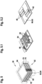
- Figures 5, 5.1 and 5.2 show additively manufactured energy collector modules.
- first comb structure 80, the parting plane 78, the second comb structure 82, another parting plane 78 and the circuit board 84 are embedded within the housing 30 produced here using the additive manufacturing process.
- the components mentioned are located in the walls of the housing 30 in the clamping areas 58, as they are analogous to the representations according to the Figures 3.1, 3.2 and 3.3 are manufactured.
- a mounting device 86 is located on the side of the housing 30 of the energy collector 28. The energy is introduced into the housing 30 in the form of vibrations or oscillations via this and is converted from mechanical to electrical energy via the respective comb structures 80 or 82, which can be equipped with additional masses 48 on the top and/or bottom.
- FIG. 5.1 An assembly 88 of the circuit board 84 with electronic components 90 is provided.
- the Figures 5, 5.1 and 5.2 The structure shown represents a 3D structure, in particular a 3D dispenser structure, and allows the first comb structure 80, the second comb structure 82, the separation planes 78 and the circuit board 84, which can be equipped with a number of electronic components 90, to be cast or attached during the manufacture of the housing 30.
- the components mentioned are shown in perspective Figure 5 arranged one above the other in the housing 30.
- Figures 5.1 and 5.2 represent detailed representations of the first comb structure 80 and the second comb structure 82 as well as the circuit board 84.
- the additional masses 48 are only shown on the upper side of the first comb structure 80 or the second comb structure 82, these can (see sectional view according to Figure 4 ) either on the top or on the bottom or on the top and bottom.
- the additional masses 48 are, for example, embedded with their ends in slot-shaped recesses and arranged one above the other in the housing 30.
- Figure 5.1 shows that the circuit board 84 shown there accommodates on its upper side a number of electronic components 90 which serve for the power management of the energy collector 28 in the installed state.
Landscapes
- Chemical & Material Sciences (AREA)
- Engineering & Computer Science (AREA)
- Materials Engineering (AREA)
- Manufacturing & Machinery (AREA)
- Physics & Mathematics (AREA)
- Mechanical Engineering (AREA)
- Optics & Photonics (AREA)
Description
- Die Erfindung bezieht sich auf ein Verfahren zur Herstellung eines Gehäuses einer Energiesammelvorrichtung mittels eines additiven Fertigungsverfahrens, wie beispielsweise des 3D-Druckverfahrens, insbesondere des 3D-Dispensens. Des Weiteren bezieht sich die Erfindung auf die Verwendung des Verfahrens zur Herstellung von Gehäusen, beispielsweise für energieautarke Sensorsysteme.
-
EP 2 078 312 B1 hat eine mittels Print-Forming-Verfahren hergestellte Energiesammelvorrichtung zum Gegenstand. Die Vorrichtung umfasst ein Gehäuse, das einen Bodenabschnitt mit einem Randwandabschnitt umfasst, die integral ausgebildet sind, indem ein Rand im Umfang des Bodenabschnitts aufgebaut wird, wobei der Bodenabschnitt ein oder mehrere Löcher umfasst, um das Abfließen von Opfermaterial während eines Print-Forming-Prozesses zu ermöglichen, der während der Herstellung der Vorrichtung verwendet wird. Des Weiteren ist ein piezoelektrisch freitragender Balken vorgesehen, der integral als Teil des Randwandabschnitts ausgebildet ist und über einen Bereich des Bodenabschnitts hinausragt, wobei der piezoelektrische freitragende Balken eine erste Elektrodenschicht, eine Keramikschicht, die auf der ersten Elektrodenschicht angeordnet ist, und eine zweite Elektrodenschicht aufweist, die auf der Keramikschicht angeordnet ist. Es ist ein erster Durchgang vorgesehen, der innerhalb des Randwandabschnitts ausgebildet ist und mit der ersten Elektrodenschicht gekoppelt ist. Des Weiteren ist ein zweiter Durchgangvorgesehen, der innerhalb des Randwandabschnitts ausgebildet ist und mit der zweiten Elektrodenschicht gekoppelt ist. Eine Zusatzmasse ist an dem piezoelektrischen freitragenden Balken angebracht. Ein Hohlraum trennt den freitragenden Balken von dem Bodenabschnitt, wobei der Hohlraum dafür eingerichtet ist, es mindestens einem Ende des freitragenden Balkens zu ermöglichen, sich vertikal relativ zum Bodenabschnitt in Reaktion auf eine sich bewegende Vorrichtung zu bewegen, wobei der Hohlraum entsteht, wenn während des Print-Forming-Prozesses Opfermaterial durch die Löcher abfließt. Es ist ein Deckel vorgesehen, der auf einem oberen Bereich des Randwandabschnitts des Gehäuses angeordnet ist, um den piezoelektrisch freitragenden Balken innerhalb des Hohlraums abzudichten. Eine erste Oberflächenmontageinsel ist auf einer Fläche des Deckels mit dem ersten Durchganggekoppelt, eine zweite Oberflächenmontageinsel auf der Fläche des Deckels ist mit dem zweiten Durchgang gekoppelt. -
US 2018/120912 A1 bezieht sich auf ein Herstellungsverfahren einer Wärmemanagementvorrichtung einschließlich ihres Gehäuses, das hauptsächlich auf einem additiven Fertigungsverfahren basiert. -
US 2014/333011 A1 hat ein additives Fertigungsverfahren zum Gegenstand, bei dem eine Wandstruktur auf einem Druckbett hergestellt wird. Ein Trägerstück mit einer antihaftbeschichteten Oberfläche wird in der Nähe oder innerhalb der Struktur platziert, eine Materialschicht wird auf einer oder mehreren Wänden und auf dem Trägerstück additiv gefertigt, um einen Überstand zu erzeugen und das Trägerstück, nachdem das den Überstand bildende Material in einen festen Zustand zurückgekehrt oder gehärtet ist, wieder entfernt wird. -
WO 2019/147 700 A1 hat ein additives Fertigungsverfahren zum Gegenstand.US 2019/0110366 A1 betrifft ein Verfahren zum Herstellen eines Komponententrägers, wobei zumindest ein Teil des Komponententrägers als dreidimensionale Struktur ausgebildet ist. - Erfindungsgemäß wird ein Verfahren zur Herstellung eines Gehäuses einer Energiesammelvorrichtung mittels additiver Fertigung, insbesondere mittels 3D-Dispensens mit zumindest nachfolgenden Verfahrensschritten vorgeschlagen:
- a) Herstellung eines additiven Schichtaufbaus des Gehäuses in eine Raumrichtung,
- b) Erzeugung von Einspannbereichen für Energiesammelstrukturen, Biegebalken, Kammstrukturen mit mindestens einer Zusatzmasse, Trennebenen und mindestens einer Leiterplatte durch additiven Schichtaufbau während der Durchführung von Verfahrensschritt a),
- c) stoffschlüssiges Fügen der in Verfahrensschritt b) genannten Komponenten in den Einspannbereichen durch Anordnung der Komponenten zwischen UV-vorvernetzten und durch additiven Schichtaufbau hergestellten Ebenen und Nassschichten im Schichtaufbau.
- In vorteilhafter Weise kann durch die erfindungsgemäß vorgeschlagene Lösung ein Gehäuse einer Energiesammelvorrichtung durch additive Herstellung bereitgestellt werden, welches einen hohen Funktionalisierungsgrad aufweist. Der hohe Funktionalisierungsgrad kann insbesondere durch ein kunststoffbasiertes Extrusionsverfahren herbeigeführt werden, wobei die Funktionalisierung in einem Fertigungsprozess erreicht werden kann.
- In vorteilhafter Weise kann durch das erfindungsgemäß vorgeschlagene Verfahren ein Material, insbesondere als Aufbaumaterial, als kationisch polymerisierbares Expoxidharz eingesetzt werden. Mittels dieses Materials lassen sich die Materialeigenschaften des erhaltenen Gehäuses gezielt einstellen, so dass mehrere Funktionen durch das Gehäuse übernommen werden können. Zu diesen sind beispielsweise die Bereitstellung einer tragenden Struktur mit definierter Steifigkeit und Dämpfung zu zählen, ferner die Gewährleistung einer Einspannung beziehungsweise Klemmung einer Kammstruktur mittels beispielsweise einer formschlüssigen Verbindung sowie eine thermische Isolation der Energiesammel- und Elektronikebenen.
- In Weiterbildung des erfindungsgemäß vorgeschlagenen Verfahrens wird das Aufbaumaterial als dual vernetztes, insbesondere durch eine UV-Strahlungsquelle chemisch vorvernetzbares Material dargestellt.
- In vorteilhafter Weiterbildung des erfindungsgemäß vorgeschlagenen Verfahrens wird nach Aufbau des gesamten, mittels additiver Fertigungsverfahren hergestellten Gehäuses eine thermische Gesamtvernetzung durchgeführt, so dass insbesondere die Komponenten eines mehrteiligen Gehäuses eine Gesamtvernetzung erfahren und somit eine mechanische Stabilität einerseits sowie eine Kapselung gegen Umwelteinflüsse andererseits gewährleistet werden kann.
- Beim erfindungsgemäß vorgeschlagenen Verfahren weist das im additiven Schichtaufbau gefertigte Gehäuse eine definierte Steifigkeit sowie eine definierte Dämpfung auf und ist in tragender Strukturbauweise ausgeführt.
- Durch die Herstellung von Einspannbereichen während der Fertigung wird eine Einspannung oder Klemmung beispielsweise von Kammstrukturen, die mindestens eine Zusatzmasse aufweisen, sichergestellt.
- Beim erfindungsgemäß vorgeschlagenen Verfahren ist innerhalb des Gehäuses eine thermische Isolation der Kammstrukturen und/oder der Leiterplatte und deren Elektronikkomponenten gewährleistet.
- In vorteilhafter Weiterbildung des erfindungsgemäß vorgeschlagenen Verfahrens wird gemäß Verfahrensschritt c) eine stoffschlüssige Verbindung durch Verklebung der Kammstrukturen mit den UV-vernetzten Ebenen mit unvernetztem Dispensermaterial, insbesondere Nassschichten, erzeugt.
- Der durch das erfindungsgemäß vorgeschlagene Verfahren geschaffene additive Schichtaufbau wird während der Herstellung des Gehäuses, insbesondere im Bodenbereich desselben, mit Montagehilfen versehen, die zur Fixierung einzulegender Konstruktionen und/oder Leiterplatten dienen. Bei den Montagehilfen handelt es sich um Abstützungen, damit zum Beispiel Biegebalken nicht in einen darunterliegenden Hohlraum abknicken.
- In vorteilhafter Weiterbildung der erfindungsgemäß vorgeschlagenen Lösung werden innerhalb der Einspannbereiche Klebstoffwannen erzeugt, die eine insbesondere Kerbspannungsspitzen herabsetzende Geometrie aufweisen. Durch eine derartige Geometrie von Klebstoffwannen lassen sich mechanische Lastspitzen, die durch das Gehäuse aufzunehmen wären, signifikant herabsetzen, so dass eine hohe Lebensdauer erreicht werden kann.
- Des Weiteren bezieht sich die Erfindung auf die Verwendung des Verfahrens zur Herstellung von Gehäusen für energieautarke Sensorsysteme.
- Durch die erfindungsgemäß vorgeschlagene Lösung kann eine Gehäuseherstellung eines Gehäuses bereitgestellt werden, wobei während der Fertigung des Gehäuses bevorzugt im additiven Fertigungsverfahren, insbesondere 3D-Dispensen, eine Funktionsintegration erzielbar ist. Kammstrukturen mit Zusatzmassen sowie eine ein Leistungsmanagement ermöglichende, mit Elektronikkomponenten bestückte Leiterplatte können in einem Fertigungsprozess zwischen den einzelnen Druckabschnitten des 3D-Dispensens in das Gehäuse während dessen Aufbau in einer Raumrichtung eingebettet und fixiert werden.
- Wird beispielsweise als Aufbaumaterial ein Material wie kationisch polymerisierbares Epoxidharz eingesetzt, so lassen sich die Materialeigenschaften des erfindungsgemäß hergestellten Gehäuses gezielt einstellen. Damit können durch das hergestellte Gehäuse mehrere Funktionen übernommen werden, wozu die Bereitstellung einer tragenden Struktur mit einer definierten Steifigkeit und einem vorgegebenen definierten Dämpfungsverhalten zu zählen ist. Des Weiteren ist das erfindungsgemäß vorgeschlagene Gehäuse so beschaffen, dass eine Einspannung oder Klemmung der Kammstrukturen beispielsweise mittels einer formschlüssigen Verbindung innerhalb des Gehäuses gewährleistet bleibt.
- Darüber hinaus kann durch das erfindungsgemäß vorgeschlagene Fertigungsverfahren eine thermische Isolation einer Energiesammelebene sowie einer Leiterplattenebene erreicht werden. In besonders vorteilhafter Weise kann bei der Anwendung des erfindungsgemäß vorgeschlagenen Verfahrens das Aufbaumaterial durch unvollständige chemische Vernetzung als Klebstoff benutzt werden. Es lassen sich stoffschlüssige Verbindungen durch Verklebung der Kammstrukturen mit dem bedruckten Gehäuse mit nicht vorvernetztem Dispensmaterial darstellen. Daraus resultiert der Vorteil, dass eine Entlastung des Einspannbereichs durch Minimierung der Kerbspannung direkt durch den additiven Aufbau ohne aufwändige Gestaltung der Einspannvorrichtung beziehungsweise aufwändige Planung von Kraftverläufen erfolgt.
- Durch die erfindungsgemäß vorgeschlagene Lösung lässt sich des Weiteren aufgrund flexibler Adaption des Gehäuses an verschiedene mechanische Schnittstellen eine relativ hohe Produktvarianz erreichen. Als Beispiele seien hier Tannenbaumklipps, Inserts, Bohrungen und dergleichen genannt. Durch die Anwendung des 3D-Dispensens lassen sich die Vorteile dieser additiven Fertigungstechnik, d. h. eine schnelle Änderung der Geometrie ohne aufwändige Werkzeuganpassung in signifikanter Weise nutzen.
- Durch im Bodenbereich des additiv gefertigten Gehäuses ausgebildete Montagehilfen sowie die ersten Lagen der Wand- beziehungsweise Einspannbereiche für die zu bestückenden Komponenten werden gleichzeitig Montagehilfen für die dann einzulegende unterste Energiesammelebene bereitgestellt. Beim erfindungsgemäß vorgeschlagenen Verfahren können in vorteilhafter Weise separate Positionierhilfen entfallen.
- Ausführungsformen der Erfindung werden anhand der Zeichnungen und der nachfolgenden Beschreibung näher erläutert.
- Es zeigen:
- Figuren 1.1 - 1.5
- ein Prozessschema der additiven Fertigung,
- Figur 2
- eine Energiesammelvorrichtung mit schalenartigem Gehäuse mit Energiesammelstrukturen und Leiterplatte,
- Figur 3.1
- die Darstellung eines Einspannbereichs in einer Z-X-Ebene,
- Figur 3.2
- die Darstellung eines Einspannbereichs ebenfalls in Z-X-Ebene,
- Figur 3.3
- eine Ausgestaltung einer Klebstoffwanne zur Kerbspannungsentlastung,
- Figur 4
- einen Querschnitt durch eine erfindungsgemäße Energiesammelvorrichtung,
- Figur 5, 5.1
- und 5.2 eine additiv gefertigte erfindungsgemäße Energiesammelvorrichtung.
- Der Darstellung gemäß der Figurensequenz 1.1 bis 1.5 ist eine Prozessdarstellung des 3D-Dispensens zu entnehmen.
- Ein dreidimensionales Modell wird zur Vorbereitung einer 3D-Dispens-Fertigung in einzelne quasi zweidimensionale Schichten aufgeteilt. Ein erstes aufgebautes Objekt 10 wird mittels 3D-Dispensen additiv Einzelschicht 12 für Einzelschicht 12 aufgebaut. Die Einzelschichten 12 werden entsprechend ihrer Geometrie durch einen Dispenserkopf abgefahren und mit entsprechendem Aufbaumaterial ausgefüllt. Nachdem eine Einzelschicht 12 aufgebaut ist, wird diese über eine UV-Strahlungsquelle 14 chemisch vorvernetzt.
-
Figur 1.2 zeigt ein zweites aufgebautes Objekt 16, welches durch Einzelschichten 12 in vertikaler Richtung aufgebaut wird, wobei eine jede Einzelschicht 12 über eine UV-Strahlungsquelle 14 zur chemischen Vorvernetzung bestrahlt wird. - Um Hohlräume ausbilden zu können, können auch zwei- oder mehrteilige Strukturen aufgebaut werden.
Figur 1.3 zeigt beispielsweise ein kastenförmig ausgebildetes erstes aufgebautes Objekt 10, welches aus Einzelschichten 12 aufgebaut wird. Entsprechend der Länge der Einzelschichten 12 ergibt sich ein Hohlraum. An einer Kontaktfläche 18 wird eine Nassschicht 20 aus Aufbaumaterial aufgebracht. Anschließend wird, wie inFigur 1.4 dargestellt ist, ein zweites aufgebautes Objekt 16 auf die mit der Nassschicht 20 beschichteten Kontaktflächen 18 aufgebracht. Dabei wird das zweite aufgebaute Objekt 16 von einem Förderwerkzeug 22 ergriffen und auf die Kontaktflächen 18 aufgebracht. - Schließlich erfolgt in
Figur 1.5 ein Aushärtevorgang 24, bei dem eine chemische Vollvernetzung sämtlicher Einzelschichten 12 des miteinander gefügten ersten aufgebauten Objekts 10 und des zweiten aufgebauten Objekts 16 bewirkt wird. -
Figur 2 zeigt eine isometrische Ansicht eines schalenartigen Gehäuses eines Energiesammlers. Bei diesem Energiesammler wird ein Gehäuse 30, das eine Profilnut 32 umfassen kann, mit einer ersten Lage 34, einer darüber liegenden zweiten Lage 36 sowie einer dritten Lage 38 in Z-Richtung 40 gesehen befüllt. Über einzelne Abstandhalter 44 wird eine Einspannung 42 der jeweiligen Lagen 34, 36, 38 vorgenommen. Die Wand des Gehäuses 30 gemäß der Darstellung inFigur 2 ist mit einem Normstecker 46 versehen. Der Normstecker 46 stellt einen additiv erzeugten Durchbruch beziehungsweise eine Öffnung im Gehäuse 30 dar, was eine potenzielle Schwachstelle für die Wand des Gehäuses 30 bildet. Wie aus der isometrischen Ansicht gemäßFigur 2 des Weiteren hervorgeht, sind die erste Lage 34 sowie die zweite Lage 36 jeweils mit einer Anzahl von Zusatzmassen 48 versehen. Am Gehäuse 30 befindet sich des Weiteren eine Montagemöglichkeit 50 an einer Vibrationsquelle. - Der Figurensequenz der
Figuren 3.1, 3.2 und 3.3 sind verschiedene Varianten von Einspannbereichen 58 zu entnehmen, mittels derer einzelne Sammelstrukturen 56 in einem Gehäuse 30, welches durch einen additiven Schichtaufbau 64 in Z-Richtung 40 beispielsweise aufgebaut wird, enthalten. AusFigur 3.1 geht beispielsweise hervor, dass im dort dargestellten Einspannbereich 58 des additiven Schichtaufbaus 64 zwischen UV-vorvernetzten Ebenen 60 eine Sammelstruktur 56 fixiert ist. Bei der Sammelstruktur 56 handelt es sich beispielsweise um einen Biegebalken 68 oder dergleichen. Wie aus dem Koordinatensystem gemäßFigur 3.1 zu entnehmen ist, erfolgt der additive Schichtaufbau 64 in Z-Richtung (vgl. Position 40). Senkrecht dazu erstreckt sich eine X-Richtung 52. Aus der Zeichenebene gemäß derFigur 3.1 ragt eine Y-Richtung 54 hervor. - Innerhalb des Einspannbereichs 58 gemäß der Darstellung in
Figur 3.1 wird das Ende der Sammelstruktur 56, die von einer Nassschicht 62 aus nicht vernetztem Aufbaumaterial gebildet ist, im Einspannbereich 58 eingegossen und fixiert. Im Ausführungsbeispiel des Einspannbereichs 58 gemäßFigur 3.1 erfolgt der additive Schichtaufbau 64 in Z-Richtung 40 in Balkendickenrichtung 74, die mit der Z-Richtung 40 zusammenfällt. - Aus der Darstellung gemäß
Figur 3.2 geht hervor, dass dort ebenfalls in Z-Richtung 40, die mit der Balkenbiegerichtung 74 zusammenfällt, ein additiver Schichtaufbau 64 vorliegt. Innerhalb des additiven Schichtaufbaus 64 werden UV-vorvernetzte Ebenen 60 aufgebaut, die einen Einspannbereich 58 begrenzen, in dem das Ende der beispielsweise als Biegebalken 68 ausgebildeten Sammelstruktur 56 eingespannt wird. Diese ist von einer Nassschicht 62 aus nicht vernetztem Aufbaumaterial umgeben. - Gemäß den Ausführungsvarianten der
Figuren 3.1 und 3.2 erfolgt der additive Schichtaufbau 64 in Balkenbiegerichtung 74, d. h. in Z-Richtung 40. -
Figur 3.3 zeigt eine Hochkantlage 66 einer Sammelstruktur 56. Ein Ende derselben ist in einer Klebstoffwanne 70 aufgenommen, die mit nicht vernetztem Aufbaumaterial befüllt ist. Die Klebstoffwanne 70 ist derart konfiguriert, dass sich eine Kerbspannungsentlastung 72 einstellt, was eine vorteilhafte Entspannung beispielsweise des Biegebalkens 68 ermöglicht. Aus der Darstellung gemäßFigur 3.3 geht hervor, dass die Klebstoffwanne 70 in der X-Y-Ebene liegt, die durch die X-Richtung 52 sowie die Y-Richtung 54 begrenzt ist. Senkrecht zu der Zeichenebene gemäß derFigur 3.3 erstreckt sich die Z-Richtung 40 aus der Zeichenebene derFigur 3.3 . - In Bezug auf
Figur 3.3 sei angemerkt, dass dort das in der Klebstoffwanne 70 bevorratete Aufbaumaterial vollständig vernetzt ist und daher als Klebstoff benutzt werden kann. Eine stoffschlüssige Verbindung kann durch Verkleben des Biegebalkens 68 mit dem bereits aufgebauten Gehäuse 30 mit nicht vorvernetztem Aufbaumaterial erreicht werden. Dadurch kann in vorteilhafter Weise eine Entlastung des Einspannbereichs 58 durch Minimierung der Kerbspannung direkt durch den additiven Schichtaufbau 64 ohne aufwändige Gestaltung der Einspannvorrichtung beziehungsweise deren Kraftverläufe geschaffen werden. - Der Darstellung gemäß
Figur 4 ist ein Gehäuse 30 eines erfindungsgemäß vorgeschlagenen Energiesammlers 28 (Harvester) zu entnehmen. AusFigur 4 geht hervor, dass das Gehäuse 30 ausgehend von dessen Bodenbereich, in dem die Montagevorrichtung 86 liegt, mehrere Ebenen enthält. Zuunterst liegt eine erste Kammstruktur 80, die an ihrer Ober- und Unterseite jeweils mit Zusatzmassen 48 versehen ist. Oberhalb der ersten Kammstruktur 80 verläuft eine Trennebene 78, über der sich - parallel zur ersten Kammstruktur 80 - eine zweite Kammstruktur 82 erstreckt. Auch die zweite Kammstruktur 82 ist an ihrer Ober- beziehungsweise ihrer Unterseite jeweils mit Zusatzmassen 48 versehen. Oberhalb der zweiten Kammstruktur 82 wiederum verläuft eine Trennebene 78, über der innerhalb des Gehäuses 30 eine Leiterplatte 84, die mit elektronischen Bauelementen an Ober- und/oder Unterseite bestück ist, verläuft. Sämtliche Komponenten, d. h. erste Kammstruktur 80, zweite Kammstruktur 82, Trennebenen 78 sowie die Leiterplatte 84 sind innerhalb des Gehäuses 30 übereinanderliegend aufgebaut und jeweils in die Ränder des Gehäuses 30, die sukzessive in Z-Richtung 40 aus Aufbaumaterial aufgebaut werden, in Einspannbereiche 58 eingespannt oder eingeklemmt, wie sie aus den zuvor beschriebenenFiguren 3.1, 3.2 und 3.3 entnehmbar sind. - Die Trennebenen 78 zwischen den einzelnen Kammstrukturen 80, 82 dienen zur thermischen Isolation.
-
Figuren 5, 5.1 und 5.2 zeigen additiv gefertigte Energiesammlermodule. - Aus
Figur 5 lässt sich entnehmen, dass innerhalb des hier im additiven Fertigungsverfahren erzeugten Gehäuses 30 die erste Kammstruktur 80, die Trennebene 78, die zweite Kammstruktur 82, erneut eine Trennebene 78 sowie die Leiterplatte 84 eingelassen sind. Die genannten Komponenten befinden sich in den Wänden des Gehäuses 30 in den Einspannbereichen 58, wie sie analog zu den Darstellungen gemäß denFiguren 3.1, 3.2 und 3.3 gefertigt sind. Seitlich am Gehäuse 30 des Energiesammlers 28 befindet sich eine Montagevorrichtung 86. Über diese wird die Energie in Form von Vibrationen beziehungsweise Schwingungen in das Gehäuse 30 eingetragen und dort über die jeweiligen Kammstrukturen 80 beziehungsweise 82, die an Ober- und/oder Unterseite mit Zusatzmassen 48 bestückt sein können, von mechanischer in elektrische Energie umgewandelt. Aus der Darstellung gemäßFigur 5.1 ergibt sich, dass eine Bestückung 88 der Leiterplatte 84 mit Elektronikkomponenten 90 vorgesehen ist. Der in denFiguren 5, 5.1 und 5.2 dargestellte Aufbau stellt einen 3D-Aufbau, insbesondere einen 3D-Dispenseraufbau dar und erlaubt während der Herstellung des Gehäuses 30 das Eingießen beziehungsweise Befestigen der im Gehäuse 30 anzuordnenden ersten Kammstruktur 80, der zweiten Kammstruktur 82, der Trennebenen 78 sowie der Leiterplatte 84, die mit einer Anzahl von Elektronikkomponenten 90 bestückt sein kann. Die genannten Komponenten sind in der perspektivisch dargestelltenFigur 5 im Gehäuse 30 übereinanderliegend angeordnet.Figuren 5.1 und 5.2 stellen jeweils Detaildarstellungen der ersten Kammstruktur 80 und der zweiten Kammstruktur 82 sowie der Leiterplatte 84 dar. - Wenngleich in der Darstellung gemäß
Figur 5.2 die Zusatzmassen 48 lediglich auf der Oberseite der ersten Kammstruktur 80 beziehungsweise der zweiten Kammstruktur 82 dargestellt sind, können diese (vgl. Schnittdarstellung gemäßFigur 4 ) sowohl an der Oberseite oder an der Unterseite oder an Unter- und Oberseite aufgenommen sein. Die Zusatzmassen 48 sind beispielsweise in schlitzförmigen Ausnehmungen mit ihren Enden eingelassen und übereinanderliegend im Gehäuse 30 angeordnet.Figur 5.1 zeigt, dass die dort dargestellte Leiterplatte 84 auf ihrer Oberseite eine Anzahl von Elektronikkomponenten 90 aufnimmt, die dem Leistungsmanagement des Energiesammlers 28 im eingebauten Zustand dienen.
Claims (11)
- Verfahren zur Herstellung eines Gehäuses (30) einer Energiesammelvorrichtung (28) mittels additiver Fertigung, insbesondere mittels 3D-Dispensens mit zumindest nachfolgenden Verfahrensschritten:a) Herstellung eines Schichtaufbaus (64) des Gehäuses (30) in eine Raumrichtung (40),b) Erzeugung von Einspannbereichen (58) für Energiesammelstrukturen (56), Biegebalken (68), Kammstrukturen (80, 82) mit mindestens einer Zusatzmasse (48), Trennebenen (78) und mindestens einer Leiterplatte (84) durch additiven Schichtaufbau während der Durchführung von Verfahrensschritt a),c) stoffschlüssiges Fügen der in Verfahrenschritt b) genannten Komponenten in den Einspannbereichen (58) durch Anordnung der Komponenten zwischen UV-vorvernetzten und durch additiven Schichtaufbau hergestellten Ebenen (60) und Nassschichten (62) im Schichtaufbau (64).
- Verfahren gemäß Anspruch 1, dadurch gekennzeichnet, dass als Aufbaumaterial kationisch polymerisierbare Epoxidharze verarbeitet werden.
- Verfahren gemäß den Ansprüchen 1 und 2, dadurch gekennzeichnet, dass das Aufbaumaterial dual vernetzbar, insbesondere durch eine UV-Strahlungsquelle (14), chemisch vorvernetzt wird.
- Verfahren gemäß den Ansprüchen 1 bis 3, dadurch gekennzeichnet, dass nach Aufbau des gesamten Gehäuses (30) eine thermische Gesamtvernetzung durchgeführt wird.
- Verfahren gemäß den Ansprüchen 1 bis 4, dadurch gekennzeichnet, dass das im additiven Schichtaufbau (64) gefertigte Gehäuse (30) in definierter Steifigkeit und definierter Dämpfung als tragende Struktur ausgeführt wird.
- Verfahren gemäß den Ansprüchen 1 bis 5, dadurch gekennzeichnet, dass im Einspannbereich (58) eine Einspannung oder Klemmung der Kammstrukturen (80, 82) sichergestellt wird.
- Verfahren gemäß den Ansprüchen 1 bis 6, dadurch gekennzeichnet, dass im Gehäuse (30) eine thermische Isolation der Kammstrukturen (80, 82) und/oder der Leiterplatte (84) und deren Elektronikkomponenten (90) gewährleistet wird.
- Verfahren gemäß den Ansprüchen 1 bis 7, dadurch gekennzeichnet, dass gemäß Verfahrensschritt c) eine stoffschlüssige Verbindung durch Verklebung der Kammstrukturen (80, 82) mit den UV-vorvernetzten Ebenen (60) mit unvernetztem Dispensermaterial, insbesondere mit Nassschichten (62) erzeugt wird.
- Verfahren gemäß den Ansprüchen 1 bis 8, dadurch gekennzeichnet, dass beim additiven Schichtaufbau (64) im Bodenbereich des Gehäuses (30) Montagehilfen für einzulegende Kammstrukturen (80, 82) und/oder Leiterplatten (84) hergestellt werden.
- Verfahren gemäß den Ansprüchen 1 bis 9, dadurch gekennzeichnet, dass innerhalb der Einspannbereiche (58) Klebstoffwannen (70) erzeugt werden, die eine eine Kerbspannung verringernde Geometrie aufweisen.
- Verwendung des Verfahrens gemäß einem der vorstehenden Ansprüche zur Herstellung von Gehäusen (30) für energieautarke Sensorsysteme.
Applications Claiming Priority (1)
| Application Number | Priority Date | Filing Date | Title |
|---|---|---|---|
| DE102020209967.7A DE102020209967A1 (de) | 2020-08-06 | 2020-08-06 | Verfahren zur Herstellung eines Gehäuses eines Energiewandlers |
Publications (2)
| Publication Number | Publication Date |
|---|---|
| EP3950274A1 EP3950274A1 (de) | 2022-02-09 |
| EP3950274B1 true EP3950274B1 (de) | 2024-05-01 |
Family
ID=76942925
Family Applications (1)
| Application Number | Title | Priority Date | Filing Date |
|---|---|---|---|
| EP21185894.9A Active EP3950274B1 (de) | 2020-08-06 | 2021-07-15 | Verfahren zur herstellung eines gehäuses einer energiesammelvorrichtung |
Country Status (3)
| Country | Link |
|---|---|
| EP (1) | EP3950274B1 (de) |
| DE (1) | DE102020209967A1 (de) |
| ES (1) | ES2983986T3 (de) |
Family Cites Families (9)
| Publication number | Priority date | Publication date | Assignee | Title |
|---|---|---|---|---|
| US6562278B1 (en) | 2000-08-29 | 2003-05-13 | Micron Technology, Inc. | Methods of fabricating housing structures and micromachines incorporating such structures |
| US7414351B2 (en) | 2006-10-02 | 2008-08-19 | Robert Bosch Gmbh | Energy harvesting device manufactured by print forming processes |
| US9555582B2 (en) | 2013-05-07 | 2017-01-31 | Google Technology Holdings LLC | Method and assembly for additive manufacturing |
| SG11201510615SA (en) | 2013-06-24 | 2016-01-28 | Harvard College | Printed three-dimensional (3d) functional part and method of making |
| US10054995B2 (en) | 2016-10-27 | 2018-08-21 | Microsoft Technology Licensing, Llc | Additive manufactured passive thermal enclosure |
| DE102017202000A1 (de) * | 2017-02-08 | 2018-08-09 | Technische Universität Dresden | Verfahren und Vorrichtung zum Einbetten mindestens eines elektronischen Bauelements in einen Träger |
| DE102017123307A1 (de) * | 2017-10-06 | 2019-04-11 | At & S Austria Technologie & Systemtechnik Aktiengesellschaft | Komponententräger mit zumindest einem Teil ausgebildet als dreidimensional gedruckte Struktur |
| EP3743262B1 (de) | 2018-01-23 | 2021-12-01 | Local Motors IP, LLC | Generativ gefertigte struktur und verfahren zur herstellung davon |
| US20200206972A1 (en) | 2018-12-31 | 2020-07-02 | Douglas Ray Sparks | Methods of making monolithic structures and devices and monolithic structures and devices made therefrom |
-
2020
- 2020-08-06 DE DE102020209967.7A patent/DE102020209967A1/de active Pending
-
2021
- 2021-07-15 ES ES21185894T patent/ES2983986T3/es active Active
- 2021-07-15 EP EP21185894.9A patent/EP3950274B1/de active Active
Also Published As
| Publication number | Publication date |
|---|---|
| ES2983986T3 (es) | 2024-10-28 |
| DE102020209967A1 (de) | 2022-02-10 |
| EP3950274A1 (de) | 2022-02-09 |
Similar Documents
| Publication | Publication Date | Title |
|---|---|---|
| DE2353615C2 (de) | Verfahren zum Herstellen eines elektrischen Verbinders | |
| DE102005041058A1 (de) | Verfahren zur Herstellung einer mehrschichtigen Karte | |
| DE112004001727T5 (de) | Verfahren zur Herstellung eines elektronischen Moduls | |
| EP2566308B1 (de) | Verfahren zur Bestückung einer Leiterplatte | |
| DE69615792T2 (de) | Miniatur-halbleiteranordnung für oberflächenmontage | |
| DE112005001414T5 (de) | Verfahren zur Herstellung eines Elektronikmoduls | |
| DE102006005645B4 (de) | Stapelbarer Baustein, Bausteinstapel und Verfahren zu deren Herstellung | |
| DE102012220823B4 (de) | Ferrule eines steckverbinders für mehrschichtige wellenleiter, steckverbinder und verfahren | |
| DE2225825B2 (de) | Verfahren zum Herstellen einer Anzahl plättchenförmiger Festkörper-Elektrolytkondensatoren | |
| EP3134907B1 (de) | Verfahren zum herstellen eines induktionsbauteils | |
| DE102013213073A1 (de) | Verfahren zum Herstellen eines optoelektronischen Bauelementes | |
| DE3149641A1 (de) | "eleketrische schaltungsplatte und verfahren zu ihrer herstellung" | |
| EP0429877B1 (de) | Vorrichtung zum Positionieren von Lichtleitfasern in Verbindungselementen | |
| EP0495778B1 (de) | Filter-steckverbinder | |
| DE102019216437A1 (de) | Mikrofon und Herstellungsverfahren dafür | |
| CH667359A5 (de) | Verfahren zur herstellung einer starre und flexible partien aufweisenden leiterplatte fuer gedruckte elektrische schaltungen. | |
| DE102016220678A1 (de) | Druckvorrichtung und Druckverfahren zum Auftragen eines viskosen oder pastösen Materials | |
| EP3950274A1 (de) | Verfahren zur herstellung eines gehäuses eines energiewandlers | |
| WO2001037622A2 (de) | Leiterbahnträgerschicht zur einlaminierung in eine chipkarte, verfahren zur herstellung einer leiterbahnträgerschicht spritzgusswerkzeug zur durchführung des verfahrens zur herstellung einer leiterbahnträgerschicht | |
| DE4423842C2 (de) | Steckverbinder für Lichtwellenleiter und Formeinsatz zur Herstellung desselben | |
| DE102020209968A1 (de) | Verfahren zur Herstellung einer elektrischen und einer mechanischen Verbindung | |
| DE112012002860T5 (de) | Solarzellenmodul auf geformtem Lead-Frame und Herstellungsverfahren | |
| EP1004226B1 (de) | Verfahren und vorrichtung zur herstellung von drahtgeschriebenen leiterplatten | |
| WO2002067642A1 (de) | Verfahren zur herstellung einer multiwire-leiterplatte und nach diesem verfahren hergestellte multiwire-leiterplatte | |
| DE112011105412B4 (de) | Elektronische Einheit |
Legal Events
| Date | Code | Title | Description |
|---|---|---|---|
| PUAI | Public reference made under article 153(3) epc to a published international application that has entered the european phase |
Free format text: ORIGINAL CODE: 0009012 |
|
| STAA | Information on the status of an ep patent application or granted ep patent |
Free format text: STATUS: THE APPLICATION HAS BEEN PUBLISHED |
|
| AK | Designated contracting states |
Kind code of ref document: A1 Designated state(s): AL AT BE BG CH CY CZ DE DK EE ES FI FR GB GR HR HU IE IS IT LI LT LU LV MC MK MT NL NO PL PT RO RS SE SI SK SM TR |
|
| STAA | Information on the status of an ep patent application or granted ep patent |
Free format text: STATUS: REQUEST FOR EXAMINATION WAS MADE |
|
| 17P | Request for examination filed |
Effective date: 20220809 |
|
| RBV | Designated contracting states (corrected) |
Designated state(s): AL AT BE BG CH CY CZ DE DK EE ES FI FR GB GR HR HU IE IS IT LI LT LU LV MC MK MT NL NO PL PT RO RS SE SI SK SM TR |
|
| GRAP | Despatch of communication of intention to grant a patent |
Free format text: ORIGINAL CODE: EPIDOSNIGR1 |
|
| STAA | Information on the status of an ep patent application or granted ep patent |
Free format text: STATUS: GRANT OF PATENT IS INTENDED |
|
| INTG | Intention to grant announced |
Effective date: 20231130 |
|
| GRAS | Grant fee paid |
Free format text: ORIGINAL CODE: EPIDOSNIGR3 |
|
| GRAA | (expected) grant |
Free format text: ORIGINAL CODE: 0009210 |
|
| STAA | Information on the status of an ep patent application or granted ep patent |
Free format text: STATUS: THE PATENT HAS BEEN GRANTED |
|
| AK | Designated contracting states |
Kind code of ref document: B1 Designated state(s): AL AT BE BG CH CY CZ DE DK EE ES FI FR GB GR HR HU IE IS IT LI LT LU LV MC MK MT NL NO PL PT RO RS SE SI SK SM TR |
|
| REG | Reference to a national code |
Ref country code: GB Ref legal event code: FG4D Free format text: NOT ENGLISH |
|
| REG | Reference to a national code |
Ref country code: CH Ref legal event code: EP |
|
| REG | Reference to a national code |
Ref country code: DE Ref legal event code: R096 Ref document number: 502021003536 Country of ref document: DE |
|
| REG | Reference to a national code |
Ref country code: IE Ref legal event code: FG4D Free format text: LANGUAGE OF EP DOCUMENT: GERMAN |
|
| REG | Reference to a national code |
Ref country code: LT Ref legal event code: MG9D |
|
| REG | Reference to a national code |
Ref country code: NL Ref legal event code: MP Effective date: 20240501 |
|
| PG25 | Lapsed in a contracting state [announced via postgrant information from national office to epo] |
Ref country code: IS Free format text: LAPSE BECAUSE OF FAILURE TO SUBMIT A TRANSLATION OF THE DESCRIPTION OR TO PAY THE FEE WITHIN THE PRESCRIBED TIME-LIMIT Effective date: 20240901 |
|
| PG25 | Lapsed in a contracting state [announced via postgrant information from national office to epo] |
Ref country code: BG Free format text: LAPSE BECAUSE OF FAILURE TO SUBMIT A TRANSLATION OF THE DESCRIPTION OR TO PAY THE FEE WITHIN THE PRESCRIBED TIME-LIMIT Effective date: 20240501 |
|
| PG25 | Lapsed in a contracting state [announced via postgrant information from national office to epo] |
Ref country code: FI Free format text: LAPSE BECAUSE OF FAILURE TO SUBMIT A TRANSLATION OF THE DESCRIPTION OR TO PAY THE FEE WITHIN THE PRESCRIBED TIME-LIMIT Effective date: 20240501 Ref country code: HR Free format text: LAPSE BECAUSE OF FAILURE TO SUBMIT A TRANSLATION OF THE DESCRIPTION OR TO PAY THE FEE WITHIN THE PRESCRIBED TIME-LIMIT Effective date: 20240501 |
|
| PG25 | Lapsed in a contracting state [announced via postgrant information from national office to epo] |
Ref country code: GR Free format text: LAPSE BECAUSE OF FAILURE TO SUBMIT A TRANSLATION OF THE DESCRIPTION OR TO PAY THE FEE WITHIN THE PRESCRIBED TIME-LIMIT Effective date: 20240802 |
|
| PG25 | Lapsed in a contracting state [announced via postgrant information from national office to epo] |
Ref country code: PT Free format text: LAPSE BECAUSE OF FAILURE TO SUBMIT A TRANSLATION OF THE DESCRIPTION OR TO PAY THE FEE WITHIN THE PRESCRIBED TIME-LIMIT Effective date: 20240902 |
|
| PG25 | Lapsed in a contracting state [announced via postgrant information from national office to epo] |
Ref country code: NL Free format text: LAPSE BECAUSE OF FAILURE TO SUBMIT A TRANSLATION OF THE DESCRIPTION OR TO PAY THE FEE WITHIN THE PRESCRIBED TIME-LIMIT Effective date: 20240501 |
|
| PG25 | Lapsed in a contracting state [announced via postgrant information from national office to epo] |
Ref country code: PL Free format text: LAPSE BECAUSE OF FAILURE TO SUBMIT A TRANSLATION OF THE DESCRIPTION OR TO PAY THE FEE WITHIN THE PRESCRIBED TIME-LIMIT Effective date: 20240501 |
|
| REG | Reference to a national code |
Ref country code: ES Ref legal event code: FG2A Ref document number: 2983986 Country of ref document: ES Kind code of ref document: T3 Effective date: 20241028 |
|
| PG25 | Lapsed in a contracting state [announced via postgrant information from national office to epo] |
Ref country code: LV Free format text: LAPSE BECAUSE OF FAILURE TO SUBMIT A TRANSLATION OF THE DESCRIPTION OR TO PAY THE FEE WITHIN THE PRESCRIBED TIME-LIMIT Effective date: 20240501 |
|
| PG25 | Lapsed in a contracting state [announced via postgrant information from national office to epo] |
Ref country code: PT Free format text: LAPSE BECAUSE OF FAILURE TO SUBMIT A TRANSLATION OF THE DESCRIPTION OR TO PAY THE FEE WITHIN THE PRESCRIBED TIME-LIMIT Effective date: 20240902 Ref country code: PL Free format text: LAPSE BECAUSE OF FAILURE TO SUBMIT A TRANSLATION OF THE DESCRIPTION OR TO PAY THE FEE WITHIN THE PRESCRIBED TIME-LIMIT Effective date: 20240501 Ref country code: NO Free format text: LAPSE BECAUSE OF FAILURE TO SUBMIT A TRANSLATION OF THE DESCRIPTION OR TO PAY THE FEE WITHIN THE PRESCRIBED TIME-LIMIT Effective date: 20240801 Ref country code: NL Free format text: LAPSE BECAUSE OF FAILURE TO SUBMIT A TRANSLATION OF THE DESCRIPTION OR TO PAY THE FEE WITHIN THE PRESCRIBED TIME-LIMIT Effective date: 20240501 Ref country code: LV Free format text: LAPSE BECAUSE OF FAILURE TO SUBMIT A TRANSLATION OF THE DESCRIPTION OR TO PAY THE FEE WITHIN THE PRESCRIBED TIME-LIMIT Effective date: 20240501 Ref country code: IS Free format text: LAPSE BECAUSE OF FAILURE TO SUBMIT A TRANSLATION OF THE DESCRIPTION OR TO PAY THE FEE WITHIN THE PRESCRIBED TIME-LIMIT Effective date: 20240901 Ref country code: HR Free format text: LAPSE BECAUSE OF FAILURE TO SUBMIT A TRANSLATION OF THE DESCRIPTION OR TO PAY THE FEE WITHIN THE PRESCRIBED TIME-LIMIT Effective date: 20240501 Ref country code: GR Free format text: LAPSE BECAUSE OF FAILURE TO SUBMIT A TRANSLATION OF THE DESCRIPTION OR TO PAY THE FEE WITHIN THE PRESCRIBED TIME-LIMIT Effective date: 20240802 Ref country code: FI Free format text: LAPSE BECAUSE OF FAILURE TO SUBMIT A TRANSLATION OF THE DESCRIPTION OR TO PAY THE FEE WITHIN THE PRESCRIBED TIME-LIMIT Effective date: 20240501 Ref country code: BG Free format text: LAPSE BECAUSE OF FAILURE TO SUBMIT A TRANSLATION OF THE DESCRIPTION OR TO PAY THE FEE WITHIN THE PRESCRIBED TIME-LIMIT Effective date: 20240501 Ref country code: RS Free format text: LAPSE BECAUSE OF FAILURE TO SUBMIT A TRANSLATION OF THE DESCRIPTION OR TO PAY THE FEE WITHIN THE PRESCRIBED TIME-LIMIT Effective date: 20240801 |
|
| PG25 | Lapsed in a contracting state [announced via postgrant information from national office to epo] |
Ref country code: DK Free format text: LAPSE BECAUSE OF FAILURE TO SUBMIT A TRANSLATION OF THE DESCRIPTION OR TO PAY THE FEE WITHIN THE PRESCRIBED TIME-LIMIT Effective date: 20240501 |
|
| PG25 | Lapsed in a contracting state [announced via postgrant information from national office to epo] |
Ref country code: EE Free format text: LAPSE BECAUSE OF FAILURE TO SUBMIT A TRANSLATION OF THE DESCRIPTION OR TO PAY THE FEE WITHIN THE PRESCRIBED TIME-LIMIT Effective date: 20240501 |
|
| PG25 | Lapsed in a contracting state [announced via postgrant information from national office to epo] |
Ref country code: CZ Free format text: LAPSE BECAUSE OF FAILURE TO SUBMIT A TRANSLATION OF THE DESCRIPTION OR TO PAY THE FEE WITHIN THE PRESCRIBED TIME-LIMIT Effective date: 20240501 |
|
| PG25 | Lapsed in a contracting state [announced via postgrant information from national office to epo] |
Ref country code: SK Free format text: LAPSE BECAUSE OF FAILURE TO SUBMIT A TRANSLATION OF THE DESCRIPTION OR TO PAY THE FEE WITHIN THE PRESCRIBED TIME-LIMIT Effective date: 20240501 Ref country code: RO Free format text: LAPSE BECAUSE OF FAILURE TO SUBMIT A TRANSLATION OF THE DESCRIPTION OR TO PAY THE FEE WITHIN THE PRESCRIBED TIME-LIMIT Effective date: 20240501 |
|
| PG25 | Lapsed in a contracting state [announced via postgrant information from national office to epo] |
Ref country code: SM Free format text: LAPSE BECAUSE OF FAILURE TO SUBMIT A TRANSLATION OF THE DESCRIPTION OR TO PAY THE FEE WITHIN THE PRESCRIBED TIME-LIMIT Effective date: 20240501 |
|
| PG25 | Lapsed in a contracting state [announced via postgrant information from national office to epo] |
Ref country code: SM Free format text: LAPSE BECAUSE OF FAILURE TO SUBMIT A TRANSLATION OF THE DESCRIPTION OR TO PAY THE FEE WITHIN THE PRESCRIBED TIME-LIMIT Effective date: 20240501 Ref country code: SK Free format text: LAPSE BECAUSE OF FAILURE TO SUBMIT A TRANSLATION OF THE DESCRIPTION OR TO PAY THE FEE WITHIN THE PRESCRIBED TIME-LIMIT Effective date: 20240501 Ref country code: RO Free format text: LAPSE BECAUSE OF FAILURE TO SUBMIT A TRANSLATION OF THE DESCRIPTION OR TO PAY THE FEE WITHIN THE PRESCRIBED TIME-LIMIT Effective date: 20240501 Ref country code: EE Free format text: LAPSE BECAUSE OF FAILURE TO SUBMIT A TRANSLATION OF THE DESCRIPTION OR TO PAY THE FEE WITHIN THE PRESCRIBED TIME-LIMIT Effective date: 20240501 Ref country code: DK Free format text: LAPSE BECAUSE OF FAILURE TO SUBMIT A TRANSLATION OF THE DESCRIPTION OR TO PAY THE FEE WITHIN THE PRESCRIBED TIME-LIMIT Effective date: 20240501 Ref country code: CZ Free format text: LAPSE BECAUSE OF FAILURE TO SUBMIT A TRANSLATION OF THE DESCRIPTION OR TO PAY THE FEE WITHIN THE PRESCRIBED TIME-LIMIT Effective date: 20240501 |
|
| REG | Reference to a national code |
Ref country code: DE Ref legal event code: R097 Ref document number: 502021003536 Country of ref document: DE |
|
| PG25 | Lapsed in a contracting state [announced via postgrant information from national office to epo] |
Ref country code: MC Free format text: LAPSE BECAUSE OF FAILURE TO SUBMIT A TRANSLATION OF THE DESCRIPTION OR TO PAY THE FEE WITHIN THE PRESCRIBED TIME-LIMIT Effective date: 20240501 |
|
| REG | Reference to a national code |
Ref country code: CH Ref legal event code: PL |
|
| PLBE | No opposition filed within time limit |
Free format text: ORIGINAL CODE: 0009261 |
|
| STAA | Information on the status of an ep patent application or granted ep patent |
Free format text: STATUS: NO OPPOSITION FILED WITHIN TIME LIMIT |
|
| PG25 | Lapsed in a contracting state [announced via postgrant information from national office to epo] |
Ref country code: LU Free format text: LAPSE BECAUSE OF NON-PAYMENT OF DUE FEES Effective date: 20240715 |
|
| PG25 | Lapsed in a contracting state [announced via postgrant information from national office to epo] |
Ref country code: LU Free format text: LAPSE BECAUSE OF NON-PAYMENT OF DUE FEES Effective date: 20240715 |
|
| 26N | No opposition filed |
Effective date: 20250204 |
|
| PG25 | Lapsed in a contracting state [announced via postgrant information from national office to epo] |
Ref country code: SI Free format text: LAPSE BECAUSE OF FAILURE TO SUBMIT A TRANSLATION OF THE DESCRIPTION OR TO PAY THE FEE WITHIN THE PRESCRIBED TIME-LIMIT Effective date: 20240501 Ref country code: BE Free format text: LAPSE BECAUSE OF NON-PAYMENT OF DUE FEES Effective date: 20240731 Ref country code: CH Free format text: LAPSE BECAUSE OF NON-PAYMENT OF DUE FEES Effective date: 20240731 |
|
| REG | Reference to a national code |
Ref country code: BE Ref legal event code: MM Effective date: 20240731 |
|
| PG25 | Lapsed in a contracting state [announced via postgrant information from national office to epo] |
Ref country code: IE Free format text: LAPSE BECAUSE OF NON-PAYMENT OF DUE FEES Effective date: 20240715 |
|
| PG25 | Lapsed in a contracting state [announced via postgrant information from national office to epo] |
Ref country code: SE Free format text: LAPSE BECAUSE OF FAILURE TO SUBMIT A TRANSLATION OF THE DESCRIPTION OR TO PAY THE FEE WITHIN THE PRESCRIBED TIME-LIMIT Effective date: 20240501 |
|
| PGFP | Annual fee paid to national office [announced via postgrant information from national office to epo] |
Ref country code: ES Payment date: 20250819 Year of fee payment: 5 |
|
| PGFP | Annual fee paid to national office [announced via postgrant information from national office to epo] |
Ref country code: DE Payment date: 20250924 Year of fee payment: 5 |
|
| PGFP | Annual fee paid to national office [announced via postgrant information from national office to epo] |
Ref country code: IT Payment date: 20250731 Year of fee payment: 5 |
|
| PGFP | Annual fee paid to national office [announced via postgrant information from national office to epo] |
Ref country code: FR Payment date: 20250723 Year of fee payment: 5 Ref country code: AT Payment date: 20251020 Year of fee payment: 5 |
|
| PG25 | Lapsed in a contracting state [announced via postgrant information from national office to epo] |
Ref country code: CY Free format text: LAPSE BECAUSE OF FAILURE TO SUBMIT A TRANSLATION OF THE DESCRIPTION OR TO PAY THE FEE WITHIN THE PRESCRIBED TIME-LIMIT; INVALID AB INITIO Effective date: 20210715 |
|
| PG25 | Lapsed in a contracting state [announced via postgrant information from national office to epo] |
Ref country code: HU Free format text: LAPSE BECAUSE OF FAILURE TO SUBMIT A TRANSLATION OF THE DESCRIPTION OR TO PAY THE FEE WITHIN THE PRESCRIBED TIME-LIMIT; INVALID AB INITIO Effective date: 20210715 |
|
| GBPC | Gb: european patent ceased through non-payment of renewal fee |
Effective date: 20250715 |
|
| PG25 | Lapsed in a contracting state [announced via postgrant information from national office to epo] |
Ref country code: GB Free format text: LAPSE BECAUSE OF NON-PAYMENT OF DUE FEES Effective date: 20250715 |