EP3950261A1 - Injection mold and injection molding method - Google Patents
Injection mold and injection molding method Download PDFInfo
- Publication number
- EP3950261A1 EP3950261A1 EP21757866.5A EP21757866A EP3950261A1 EP 3950261 A1 EP3950261 A1 EP 3950261A1 EP 21757866 A EP21757866 A EP 21757866A EP 3950261 A1 EP3950261 A1 EP 3950261A1
- Authority
- EP
- European Patent Office
- Prior art keywords
- gas
- base plate
- substrate
- injection
- gas duct
- Prior art date
- Legal status (The legal status is an assumption and is not a legal conclusion. Google has not performed a legal analysis and makes no representation as to the accuracy of the status listed.)
- Granted
Links
Images




Classifications
-
- B—PERFORMING OPERATIONS; TRANSPORTING
- B29—WORKING OF PLASTICS; WORKING OF SUBSTANCES IN A PLASTIC STATE IN GENERAL
- B29C—SHAPING OR JOINING OF PLASTICS; SHAPING OF MATERIAL IN A PLASTIC STATE, NOT OTHERWISE PROVIDED FOR; AFTER-TREATMENT OF THE SHAPED PRODUCTS, e.g. REPAIRING
- B29C45/00—Injection moulding, i.e. forcing the required volume of moulding material through a nozzle into a closed mould; Apparatus therefor
- B29C45/14—Injection moulding, i.e. forcing the required volume of moulding material through a nozzle into a closed mould; Apparatus therefor incorporating preformed parts or layers, e.g. injection moulding around inserts or for coating articles
- B29C45/14639—Injection moulding, i.e. forcing the required volume of moulding material through a nozzle into a closed mould; Apparatus therefor incorporating preformed parts or layers, e.g. injection moulding around inserts or for coating articles for obtaining an insulating effect, e.g. for electrical components
- B29C45/14655—Injection moulding, i.e. forcing the required volume of moulding material through a nozzle into a closed mould; Apparatus therefor incorporating preformed parts or layers, e.g. injection moulding around inserts or for coating articles for obtaining an insulating effect, e.g. for electrical components connected to or mounted on a carrier, e.g. lead frame
-
- B—PERFORMING OPERATIONS; TRANSPORTING
- B29—WORKING OF PLASTICS; WORKING OF SUBSTANCES IN A PLASTIC STATE IN GENERAL
- B29C—SHAPING OR JOINING OF PLASTICS; SHAPING OF MATERIAL IN A PLASTIC STATE, NOT OTHERWISE PROVIDED FOR; AFTER-TREATMENT OF THE SHAPED PRODUCTS, e.g. REPAIRING
- B29C45/00—Injection moulding, i.e. forcing the required volume of moulding material through a nozzle into a closed mould; Apparatus therefor
- B29C45/17—Component parts, details or accessories; Auxiliary operations
- B29C45/26—Moulds
- B29C45/2602—Mould construction elements
-
- B—PERFORMING OPERATIONS; TRANSPORTING
- B29—WORKING OF PLASTICS; WORKING OF SUBSTANCES IN A PLASTIC STATE IN GENERAL
- B29C—SHAPING OR JOINING OF PLASTICS; SHAPING OF MATERIAL IN A PLASTIC STATE, NOT OTHERWISE PROVIDED FOR; AFTER-TREATMENT OF THE SHAPED PRODUCTS, e.g. REPAIRING
- B29C33/00—Moulds or cores; Details thereof or accessories therefor
- B29C33/10—Moulds or cores; Details thereof or accessories therefor with incorporated venting means
-
- B—PERFORMING OPERATIONS; TRANSPORTING
- B29—WORKING OF PLASTICS; WORKING OF SUBSTANCES IN A PLASTIC STATE IN GENERAL
- B29C—SHAPING OR JOINING OF PLASTICS; SHAPING OF MATERIAL IN A PLASTIC STATE, NOT OTHERWISE PROVIDED FOR; AFTER-TREATMENT OF THE SHAPED PRODUCTS, e.g. REPAIRING
- B29C45/00—Injection moulding, i.e. forcing the required volume of moulding material through a nozzle into a closed mould; Apparatus therefor
- B29C45/0025—Preventing defects on the moulded article, e.g. weld lines, shrinkage marks
-
- B—PERFORMING OPERATIONS; TRANSPORTING
- B29—WORKING OF PLASTICS; WORKING OF SUBSTANCES IN A PLASTIC STATE IN GENERAL
- B29C—SHAPING OR JOINING OF PLASTICS; SHAPING OF MATERIAL IN A PLASTIC STATE, NOT OTHERWISE PROVIDED FOR; AFTER-TREATMENT OF THE SHAPED PRODUCTS, e.g. REPAIRING
- B29C45/00—Injection moulding, i.e. forcing the required volume of moulding material through a nozzle into a closed mould; Apparatus therefor
- B29C45/14—Injection moulding, i.e. forcing the required volume of moulding material through a nozzle into a closed mould; Apparatus therefor incorporating preformed parts or layers, e.g. injection moulding around inserts or for coating articles
-
- B—PERFORMING OPERATIONS; TRANSPORTING
- B29—WORKING OF PLASTICS; WORKING OF SUBSTANCES IN A PLASTIC STATE IN GENERAL
- B29C—SHAPING OR JOINING OF PLASTICS; SHAPING OF MATERIAL IN A PLASTIC STATE, NOT OTHERWISE PROVIDED FOR; AFTER-TREATMENT OF THE SHAPED PRODUCTS, e.g. REPAIRING
- B29C45/00—Injection moulding, i.e. forcing the required volume of moulding material through a nozzle into a closed mould; Apparatus therefor
- B29C45/14—Injection moulding, i.e. forcing the required volume of moulding material through a nozzle into a closed mould; Apparatus therefor incorporating preformed parts or layers, e.g. injection moulding around inserts or for coating articles
- B29C45/14639—Injection moulding, i.e. forcing the required volume of moulding material through a nozzle into a closed mould; Apparatus therefor incorporating preformed parts or layers, e.g. injection moulding around inserts or for coating articles for obtaining an insulating effect, e.g. for electrical components
-
- B—PERFORMING OPERATIONS; TRANSPORTING
- B29—WORKING OF PLASTICS; WORKING OF SUBSTANCES IN A PLASTIC STATE IN GENERAL
- B29C—SHAPING OR JOINING OF PLASTICS; SHAPING OF MATERIAL IN A PLASTIC STATE, NOT OTHERWISE PROVIDED FOR; AFTER-TREATMENT OF THE SHAPED PRODUCTS, e.g. REPAIRING
- B29C45/00—Injection moulding, i.e. forcing the required volume of moulding material through a nozzle into a closed mould; Apparatus therefor
- B29C45/17—Component parts, details or accessories; Auxiliary operations
- B29C45/26—Moulds
- B29C45/34—Moulds having venting means
-
- B—PERFORMING OPERATIONS; TRANSPORTING
- B29—WORKING OF PLASTICS; WORKING OF SUBSTANCES IN A PLASTIC STATE IN GENERAL
- B29C—SHAPING OR JOINING OF PLASTICS; SHAPING OF MATERIAL IN A PLASTIC STATE, NOT OTHERWISE PROVIDED FOR; AFTER-TREATMENT OF THE SHAPED PRODUCTS, e.g. REPAIRING
- B29C45/00—Injection moulding, i.e. forcing the required volume of moulding material through a nozzle into a closed mould; Apparatus therefor
- B29C45/17—Component parts, details or accessories; Auxiliary operations
- B29C45/72—Heating or cooling
-
- H—ELECTRICITY
- H10—SEMICONDUCTOR DEVICES; ELECTRIC SOLID-STATE DEVICES NOT OTHERWISE PROVIDED FOR
- H10W—GENERIC PACKAGES, INTERCONNECTIONS, CONNECTORS OR OTHER CONSTRUCTIONAL DETAILS OF DEVICES COVERED BY CLASS H10
- H10W74/00—Encapsulations, e.g. protective coatings
- H10W74/01—Manufacture or treatment
- H10W74/016—Manufacture or treatment using moulds
-
- B—PERFORMING OPERATIONS; TRANSPORTING
- B29—WORKING OF PLASTICS; WORKING OF SUBSTANCES IN A PLASTIC STATE IN GENERAL
- B29C—SHAPING OR JOINING OF PLASTICS; SHAPING OF MATERIAL IN A PLASTIC STATE, NOT OTHERWISE PROVIDED FOR; AFTER-TREATMENT OF THE SHAPED PRODUCTS, e.g. REPAIRING
- B29C45/00—Injection moulding, i.e. forcing the required volume of moulding material through a nozzle into a closed mould; Apparatus therefor
- B29C45/17—Component parts, details or accessories; Auxiliary operations
- B29C45/26—Moulds
- B29C45/2669—Moulds with means for removing excess material, e.g. with overflow cavities
- B29C2045/2671—Resin exit gates or bleeder passages
-
- B—PERFORMING OPERATIONS; TRANSPORTING
- B29—WORKING OF PLASTICS; WORKING OF SUBSTANCES IN A PLASTIC STATE IN GENERAL
- B29C—SHAPING OR JOINING OF PLASTICS; SHAPING OF MATERIAL IN A PLASTIC STATE, NOT OTHERWISE PROVIDED FOR; AFTER-TREATMENT OF THE SHAPED PRODUCTS, e.g. REPAIRING
- B29C45/00—Injection moulding, i.e. forcing the required volume of moulding material through a nozzle into a closed mould; Apparatus therefor
- B29C45/17—Component parts, details or accessories; Auxiliary operations
- B29C45/26—Moulds
- B29C2045/2683—Plurality of independent mould cavities in a single mould
-
- B—PERFORMING OPERATIONS; TRANSPORTING
- B29—WORKING OF PLASTICS; WORKING OF SUBSTANCES IN A PLASTIC STATE IN GENERAL
- B29C—SHAPING OR JOINING OF PLASTICS; SHAPING OF MATERIAL IN A PLASTIC STATE, NOT OTHERWISE PROVIDED FOR; AFTER-TREATMENT OF THE SHAPED PRODUCTS, e.g. REPAIRING
- B29C45/00—Injection moulding, i.e. forcing the required volume of moulding material through a nozzle into a closed mould; Apparatus therefor
- B29C45/14—Injection moulding, i.e. forcing the required volume of moulding material through a nozzle into a closed mould; Apparatus therefor incorporating preformed parts or layers, e.g. injection moulding around inserts or for coating articles
- B29C45/14336—Coating a portion of the article, e.g. the edge of the article
- B29C45/14344—Moulding in or through a hole in the article, e.g. outsert moulding
-
- B—PERFORMING OPERATIONS; TRANSPORTING
- B29—WORKING OF PLASTICS; WORKING OF SUBSTANCES IN A PLASTIC STATE IN GENERAL
- B29L—INDEXING SCHEME ASSOCIATED WITH SUBCLASS B29C, RELATING TO PARTICULAR ARTICLES
- B29L2031/00—Other particular articles
- B29L2031/34—Electrical apparatus, e.g. sparking plugs or parts thereof
-
- H—ELECTRICITY
- H10—SEMICONDUCTOR DEVICES; ELECTRIC SOLID-STATE DEVICES NOT OTHERWISE PROVIDED FOR
- H10W—GENERIC PACKAGES, INTERCONNECTIONS, CONNECTORS OR OTHER CONSTRUCTIONAL DETAILS OF DEVICES COVERED BY CLASS H10
- H10W70/00—Package substrates; Interposers; Redistribution layers [RDL]
- H10W70/60—Insulating or insulated package substrates; Interposers; Redistribution layers
- H10W70/67—Insulating or insulated package substrates; Interposers; Redistribution layers characterised by their insulating layers or insulating parts
- H10W70/68—Shapes or dispositions thereof
- H10W70/681—Shapes or dispositions thereof comprising holes not having chips therein, e.g. for outgassing, underfilling or bond wire passage
-
- H—ELECTRICITY
- H10—SEMICONDUCTOR DEVICES; ELECTRIC SOLID-STATE DEVICES NOT OTHERWISE PROVIDED FOR
- H10W—GENERIC PACKAGES, INTERCONNECTIONS, CONNECTORS OR OTHER CONSTRUCTIONAL DETAILS OF DEVICES COVERED BY CLASS H10
- H10W72/00—Interconnections or connectors in packages
-
- H—ELECTRICITY
- H10—SEMICONDUCTOR DEVICES; ELECTRIC SOLID-STATE DEVICES NOT OTHERWISE PROVIDED FOR
- H10W—GENERIC PACKAGES, INTERCONNECTIONS, CONNECTORS OR OTHER CONSTRUCTIONAL DETAILS OF DEVICES COVERED BY CLASS H10
- H10W74/00—Encapsulations, e.g. protective coatings
-
- H—ELECTRICITY
- H10—SEMICONDUCTOR DEVICES; ELECTRIC SOLID-STATE DEVICES NOT OTHERWISE PROVIDED FOR
- H10W—GENERIC PACKAGES, INTERCONNECTIONS, CONNECTORS OR OTHER CONSTRUCTIONAL DETAILS OF DEVICES COVERED BY CLASS H10
- H10W90/00—Package configurations
- H10W90/701—Package configurations characterised by the relative positions of pads or connectors relative to package parts
- H10W90/721—Package configurations characterised by the relative positions of pads or connectors relative to package parts of bump connectors
- H10W90/724—Package configurations characterised by the relative positions of pads or connectors relative to package parts of bump connectors between a chip and a stacked insulating package substrate, interposer or RDL
Definitions
- the disclosure relates to the field of chip package, in particular to an injection mould and an injection moulding method.
- the packaged chip After a chip is packaged, the packaged chip needs to be wrapped through injection moulding, so as to protect the chip.
- the chip is connected to a circuit on a substrate by solder bumps.
- a moulding compound is required to wrap the whole chip to fill up a gap between the chip and the substrate. Since the chip and the substrate are connected directly by the solder bumps, the gap is relatively small, and a distance between solder balls is also relatively small. As a result, air is difficult to be exhausted during filling of the moulding compound, which easily leads to an unreliable package structure.
- a gas hole is arranged in a package substrate, so that the gas is exhausted from the gas hole of the substrate with the filling of the plastic package material in the injection moulding process.
- the substrate is contacted to a surface of a base plate of a package mould, and the gas hole is easily blocked, so that the problem that the gas cannot be exhausted still exists.
- the technical problem to be solved by the disclosure is to provide an injection mould and an injection moulding method to improve the reliability of a packaged chip after injection moulding.
- an injection mould which includes a base plate used to place a packaged chip to be moulded.
- the packaged chip includes a substrate and at least one of the chips fixed on a front surface of the substrate by a flip chip process, and the substrate has a gas hole penetrating through the substrate.
- Two or more gas ducts that extend in at least two intersected directions and connect with one another are formed in the base plate. Two ends of each one of the gas ducts are open, and at least one of the gas ducts is buried into the base plate.
- the gas duct is provided with a gas outlet used to connect with the gas hole of the substrate.
- At least one of the two or more gas ducts is located on the front surface of the base plate; each one of gas ducts located on the surface of the base plate is a groove located on the front surface of the base plate; and the gas duct buried into the base plate is a tunnel located inside the base plate.
- the gas ducts that extend in at least two different directions are respectively located at different depths in the base plate.
- the gas duct that extends in at least one of the directions is buried into the base plate.
- the gas outlet is located at the intersection of the different gas ducts, so that the intersected gas ducts connect with one another.
- a maximum distance between any two points on the edge of a cross section perpendicular to a length direction of the gas duct ranges from 500 ⁇ m to 5 mm.
- the size of the gas outlet of the gas duct is larger than or equal to the size of the gas hole of the substrate.
- a first gas duct extending in a first direction and a second gas duct extending in a second direction are formed in the base plate; the first gas duct is a groove formed on the surface of the base plate; the second gas duct is a tunnel buried into the base plate; and the second gas duct and the first gas duct connect with each other at the intersection.
- a step is provided at a position in the second gas duct at a connection to the first gas duct; the step is connected to the bottom of the first gas duct in an extending direction of the first gas duct; and the surface of the step is flush with the bottom surface of the first gas duct.
- the gas holes of the substrate of the packaged chip to be injection moulded are arranged in a straight line.
- the extending direction of the first gas duct is consistent with the direction in which the gas holes are arranged in the substrate, and each of the first gas ducts is used to connect to the gas holes located on the same straight line.
- the injection mould further includes a cover used to cover the base plate to form a cavity with the base plate.
- the cavity is used to accommodate the packaged chip to be injection moulded.
- the gas duct of the base plate connects the cavity with the outside the injection mould.
- the cover is provided with at least one injection hole used to inject a moulding compound to the cavity.
- the disclosure further provides an injection moulding method, the method includes following acts.
- An injection mould and a packaged chip to be injection moulded are provided.
- the packaged chip includes a substrate and at least one of the chips fixed on the front surface of the substrate by a flip chip process.
- the substrate has a gas hole penetrating through the substrate.
- the packaged chip is placed on a base plate of the injection mould.
- the base plate is covered with a cover to form a cavity.
- the packaged chip is located in the cavity.
- the back surface of the substrate is contacted to the surface of the base plate.
- the gas hole of the substrate of the packaged chip connects with a gas duct of the base plate.
- a moulding compound in the state of liquid is injected to the cavity through an injection hole of the cover. At least part of gas in the cavity is exhausted out of the injection mould through the gas hole and the gas duct in the injection process.
- the moulding compound is injected to the cavity through two or more injection holes.
- At least one of the gas holes is formed in a substrate region on which each one of the packaged chips is located.
- the method further includes: after the cavity is filled up with the liquid moulding compound, heat treatment is performed to solidify the moulding compound in the state of liquid.
- the solidified packaged chip covered with the moulding compound is taken out from the cavity.
- the base plate of the injection mould of the disclosure has the gas ducts extending multiple directions, and the gas ducts extending in various directions connect to form a mesh-type gas duct structure.
- the gas can still be exhausted through the gas duct in other directions, thereby lowering the risk that gas in an injection moulding cavity cannot be exhausted and improving the reliability of the moulded packaged chip.
- an injection mould is provided.
- a base plate of the mould is provided with a groove that can connect with a gas hole of a substrate of the packaged chip, so that gas is exhausted out of the mould from the gas hole and through the groove.
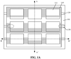
- FIG. 1A is a schematic top view
- FIG. 1B is a schematic sectional view along a cut line AA' in FIG. 1A
- FIG. 1C is a schematic sectional view along a cut line BB' in FIG. 1A .
- the packaged chip includes a substrate 110 and a chip 111 mounted on the substrate 110 by a flip chip process.
- the substrate 110 has a front surface and a back surface which are opposite, and the chip 111 is fixed on the front surface of the substrate 110.
- the packaged chip is placed in a cavity of the injection mould, and the substrate 110 is provided with a gas hole 113.
- the injection mould includes a base plate 101 and a cover 102.
- the base plate 101 has a groove 120 inside. Two ends of the groove 120 are open and connect to the exterior of the injection mould.
- the packaged chip is placed on the base plate 101, and the gas hole 113 connects with the groove 120.
- gas is exhausted out of the mould through the gas hole 113 of the substrate 110 firstly and the groove 120 of the base plate 101 secondly.
- the disclosure forms the groove 120, which connects with the gas hole 113, in the base plate 101 of the injection mould, which can further enhance the exhaust effect during injection moulding.
- the edge of the cavity in the mould will be usually filled with the moulding compound first; so that the chip 111 located at the edge position will be wrapped by the moulding compound first.
- the moulding compound overflowing from the gas hole 113 of the substrate 101 into the groove 120 may possibly block the two ends of the groove 120 at the substrate 101 (such as the position of a region 130 in FIG. 1A ) when the cavity is not filled up by the moulding compound.
- the groove 120 will not achieve a relatively good exhaust effect, and the problem that air cannot be exhausted in the injection moulding process still exists, resulting in formation of a hole between the chip 111 and the substrate 110, affecting the reliability of the device.
- the inventors further proposed a new mould to improve the above-mentioned problem.
- the injection mould includes a base plate used to place a packaged chip to be injection moulded.
- the packaged chip includes a substrate and at least one of the chips fixed on a front surface of the substrate by a flip chip process, and the substrate has a gas hole penetrating through the substrate.
- Two or more gas ducts that extend in at least two intersected directions and connect with one another are formed in the base plate. Two ends of each one of the gas ducts are open, and at least one of gas ducts is buried into the base plate.
- the gas duct is provided with a gas outlet used to connect with the gas hole of the substrate.
- FIG. 2A is a schematic top view of the base plate 210
- FIG. 2B is a schematic sectional view along a cut line CC' in FIG. 2A
- FIG. 2C is a schematic sectional view along a cut line DD' in FIG. 2A .
- the base plate 210 has a first gas duct 211 extending in a first direction and a second gas duct 212 extending in a second direction.
- the first direction is an X-axis direction
- the second direction is a Y-axis direction.
- the first direction is perpendicular to the second direction.
- the first direction and the second direction can be intersected in other angles.
- forming 3 gas ducts in each of the first direction and the second direction is taken as an example.
- the number of the gas ducts in each direction can be designed according to the structure of the packaged chip to be moulded and an actual need, and there is no limitation here.
- the base plate 210 has two opposite surfaces, i.e., a front surface and a back surface.
- the packaged chip is applied and placed on the front surface of the base plate 210.
- the first gas duct 211 is a groove formed on the front surface of the base plate 210
- the second gas duct 212 is a tunnel buried in the base plate 211.
- the second gas duct 212 and the first gas duct 211 connect with each other at an intersection.
- the first gas duct 211 and the second gas duct 212 connect with each other at the intersection, so that the first gas duct 211 and the second gas duct 212 form a mesh-type gas duct structure. Gas can also be exhausted in other directions when any one of the intersection is blocked.
- the first gas duct 211 and the second gas duct 212 are each provided with a gas outlet. An opening of one end of each gas outlet is located on the front surface of the base plate 210 and used to connect with the gas hole of the substrate of the packaged chip to be moulded.
- the first gas duct 211 is a groove. The opening of the whole groove can be used as the gas outlet of the first gas duct 211.
- the second gas duct 212 is buried in the base plate 210, and a gas duct region at a connection between the second gas duct 212 and the first gas duct 211 is used as the gas outlet of the second gas duct 212.
- the gas outlet of the second gas duct 212 is located at the intersection between the second gas duct 212 and the first gas duct 211.
- the gas holes of the substrate of the packaged chip to be moulded are arranged in a straight line.
- the extending direction of the first gas duct 211 is consistent with the direction in which the gas holes are arranged in the substrate, and each of the first gas ducts 211 connects to the gas holes located on the same straight line.
- a moulding compound enters the first gas duct from the gas hole of the substrate of the chip.
- the moulding compound strip located on the back surface of the substrate is formed in the first gas duct to close the gas hole connecting with the first gas duct, thereby enhancing the closing effect on the gas hole of the substrate.
- the first gas duct 211 has a width range of 100 ⁇ m to 1 mm. Formation of an oversized moulding compound strip on the back surface of the substrate which occupies an excessive area of the back surface of the substrate to affect the circuit distribution on the back surface of the substrate is avoided while satisfying an exhaust requirement.
- gas ducts extending in three or more directions can also be formed to improve the gas exhausting efficiency.
- the gas ducts in at least two different extending directions are respectively located at different depths of the base plate.
- the gas ducts extending in various directions are all buried into the base plate, and the gas ducts extending in different directions are buried at different depths and perpendicularly connect with one another at an intersection.
- a through hole in the intersection is used as the gas outlet of the various gas ducts to connect to the gas holes of the substrate of the packaged chip to be moulded. Therefore, in this case, the number of gas inlet can be set according to the number of the gas holes of the substrate of the packaged chip to be moulded. This quantity can be equal to or greater than the quantity of the gas holes to adapt to different kinds of packaged chips.
- the gas outlet is a circular hole with a diameter ranging from 100 ⁇ m to 1 mm, preferably 200 ⁇ m, 300 ⁇ m, 400 ⁇ m, 500 ⁇ m, 600 ⁇ m, 700 ⁇ m, or 800 ⁇ m.
- the gas outlet can also be a rectangular hole with a side ranging from 100 ⁇ m to 1 mm.
- the gas duct extending in other directions is buried into the base plate.
- the cross section of the gas duct can be circular, rectangular, semicircular, elliptical, or of other shapes.
- the extending direction of the gas duct and the number of the extending directions are not limited. Those skilled in the art can design these according to actual needs.
- the gas duct can have a relatively large cross-sectional size.
- a maximum distance between any two points on the edge of the cross section perpendicular to a length direction of the gas duct ranges from 500 ⁇ m to 5 mm.
- the maximum distance is the diameter of the cross section.
- the cross section of the gas duct is rectangular, the maximum distance is the maximum side of the cross section.
- different cross-sectional sizes can also be set according to the depths that the gas ducts are located in the base plate.
- the cross-sectional area of the lower gas duct can be larger than the cross-sectional area of the upper gas duct.
- the first gas duct 211 is the groove located on the surface of the base plate and has a rectangular cross section with side range of 500 ⁇ m to 2 mm, preferably 800 ⁇ m to 1.7 mm.
- the second gas duct 212 is located below the first gas duct 211 and has a circular cross section with a diameter range of 500 ⁇ m to 5 mm, preferably 800 ⁇ m to 4 ⁇ m. The larger the cross-sectional area of the gas duct is, the higher gas exhausting efficiency results.
- the first gas duct 211 and the second gas duct 212 are both linear gas ducts.
- the gas duct can also be curved, such as the gas duct 301 in FIG. 3 .
- the shape and extending direction of the various gas ducts can be designed according to the arrangement of the gas hole of the substrate of the chip to be packaged. Any shape and arrangement rule shall fall within the protection scope of the disclosure, and are not listed one by one here.
- FIG. 4A is a schematic top view of a surface of the base plate 410;
- FIG. 4B is a schematic sectional diagram along a cut line E-E' in FIG. 4A ;
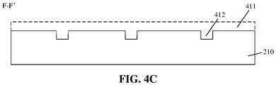
- FIG. 4C is a schematic sectional diagram along a cut line F-F' in FIG. 4A ;
- FIG. 4D is a schematic sectional diagram along a cut line G-G' in FIG. 4A .
- a first gas duct 411 extending in a first direction (x-axis) is on the surface of the base plate 410
- a second gas duct 412 extending in a second direction (y-axis) is inside the base plate 410.
- the first gas duct 411 is a groove formed on the front surface of the base plate 410
- the second gas duct 412 is a tunnel buried in the base plate 410.
- the first gas duct 411 and the second gas duct 412 connect with each other at an intersection.
- a step 413 is provided at a position in the second gas duct 412 which connects to the first gas duct 411.
- the step 413 is connected to the bottom of other positions of the first gas duct 411 in an extending direction of the first gas duct 411.
- the surface of the step 413 is flush with the bottom surface of other positions of the first gas duct 411.
- the surface of the step 413 can also be slightly higher than or lower than the bottom surface of the first gas duct 411.
- the injection mould further includes a cover used to cover the base plate to form a cavity with the base plate.
- the cavity is used to accommodate the packaged chip to be injection moulded.
- the gas duct of the base plate connects the cavity with the outside of the injection mould.
- the cover is provided with at least one injection hole used to inject the moulding compound to the cavity.
- a gas outlet hole can also be formed in the cover and used to connect the cavity to the outside of the injection mould.
- the base plate of the injection mould has the gas ducts extending in multiple directions, and the gas ducts extending in various directions connect to form a mesh-type gas duct structure.
- gas can still be exhausted through the gas duct in other directions, thereby lowering the risk that gas in an injection moulding cavity cannot be exhausted and improving the reliability of the packaged chip after injection moulding.
- the specific example of the disclosure further provides an injection moulding method.
- the method performs injection moulding on a packaged chip by using the injection mould provided in the above-mentioned specific example.
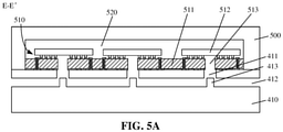
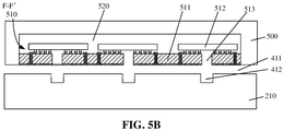
- FIG. 5A to FIG. 6B schematic structural diagrams of an injection moulding process for a packaged chip in one specific example of the disclosure are illustrated.
- the injection mould includes a base plate 400 and a cover 500.
- the specific structure of the base plate 400 refer to FIG. 4A to FIG. 4D , and details thereof are omitted here.
- a packaged chip 510 to be injection moulded is placed on the front surface of the base plate 400.
- the packaged chip 510 includes a substrate 511 and at least one of the chips 512 fixed on the front surface of the substrate 511 by a flip chip process.
- the substrate is provided with a gas hole 513.
- the cover 500 covers the surface of the base plate 400 to form a cavity 520, and the packaged chip is located in the cavity 520.
- the back surface of the substrate 511 is contacted to the surface of the base plate 410, and the gas hole 513 of the substrate 511 of the packaged chip 510 connects with a gas duct of the base plate 410.
- the front surface and the back surface of the substrate 511 are two opposite surfaces.
- the substrate 511 of the packaged chip 510 is a circuit board on which an electric connection structure such as a circuit and a solder pad is formed.
- an electric connection structure such as a circuit and a solder pad is formed.
- chips 512 are packaged on the surfaces by the flip chip process.
- the chip 512 is flipped on the surface of the substrate 511 and is electrically connected to the electric connection structure on the surface of the substrate 511 by a solder bump.
- the solder bump can be a solder ball, a copper pillar, or other structures.
- At least one of the gas holes 513 is formed in a substrate region that each chip 512 of the packaged chip 510 is located. At least part of the gas holes connects with the gas duct of the base plate 410 to exhaust air by the gas duct. Preferably, all the gas holes 513 of the substrate 511 connect with the gas duct of the base plate 410 to improve the exhaust efficiency.
- the gas hole 513 is a circular hole, the size of which is slightly less than or equal to the size of a gas outlet of the gas duct of the base plate 410.
- the diameter of the gas hole 513 is less than the width of the first gas duct 411. In one specific example, the diameter of the gas hole 513 ranges from 800 ⁇ m to 0.8 mm, and the width of the first gas duct 411 ranges from 100 ⁇ m to 1 mm.
- the base plate 410 includes a groove-like first gas duct 411 located on the front surface and a second gas duct 412 buried in the base plate 410.
- the gas holes 513 of the substrate 511 are arranged in an extending direction of the first gas duct 411.
- the gas holes 513 located on the same straight line connect to the same first gas duct 411.
- the gas ducts of the base plate can be all buried in the base plate.
- the gas outlet of the gas duct which is a hole, penetrates through to the front surface of the base plate.
- the gas hole 513 of the substrate 511 connects with at least part of the gas outlets on the front surface of the base plate.
- a moulding compound 600 in the state of liquid is injected to the cavity 520 through an injection hole (not shown) in the cover 500 (referring to FIG. 5A to FIG. 5B ).
- an injection hole (not shown) in the cover 500 (referring to FIG. 5A to FIG. 5B ).
- at least part of air in the cavity 520 is exhausted through the gas hole 513 (referring to FIG. 5A to FIG. 5B ) and the gas ducts to the outside of the injection mould.
- the flow rate is controlled so that gas in the cavity 520 has enough time to be exhausted through the gas duct.
- the injection moulding pressure intensity in the injection moulding process is controlled to range from 7E6 Pa to 1E7 Pa.
- two or more injection holes can be formed in the cover 500.
- the moulding compound can be injected to the cavity through the two or more injection holes to improve the injection efficiency.
- the cover 500 can also have a gas outlet hole (not shown).
- the gas at the upper part of the cavity 520 can be exhausted to the outside through the gas outlet hole in the cover 500, thereby reducing the volume of gas needing to be exhausted from the gas ducts of the base plate 410.
- the flow rate of the injection moulding compound can be properly increased to improve the injection moulding efficiency.
- the moulding compound 600 enters the first gas duct 411 from the gas hole of the substrate 511.
- the packaged chip 510 is taken out from the mould, carrying the moulding compound formed in the first gas duct 411, so that the back surface of the substrate 511 has a moulded strip 610.
- the moulded strip 610 closes the gas holes located on the same straight line to enhance the closing effect on the gas hole.
- groove-like gas ducts extending in multiple directions can be formed on the front surface of the base plate, so that moulded strips 610 extending in multiple directions are formed on the substrate 511 after the injection moulding is completed.
- the gas duct distribution positions on the surface of the base plate need to be reasonably set according to the positions of the electric connection structure such as the solder pads formed on the back surface of the substrate 511 to avoid the formed moulded strip 610 from affecting the connection structure on the back surface of the substrate 511.
- one step 413 is provided at the connection between the first gas duct 411 and the second gas duct 412, a connection channel between the first gas duct 411 and the second gas duct 412 is relatively narrow, and the connection intensity of the moulding compound at the connection between the first gas duct 411 and the second gas duct 412 is relatively low. Therefore, after the injection moulding is completed, in the process of taking out the packaged chip 510, the moulding compound at the connection between the first gas duct 411 and the second gas duct 412 is easy to break so that it is easy to take out the packaged chip 510. After the packaged chip 510 is taken out, the method further includes the following acts.
- a solder ball is formed on the surface of the other side of the packaged chip 510, the solder ball is electrically connected to the chip 512 on the front surface of the substrate 511 by the electric connection structure at the substrate 510; then the substrate 510 is cut to form a moulded packaged chip including a single chip 512.
Landscapes
- Engineering & Computer Science (AREA)
- Mechanical Engineering (AREA)
- Manufacturing & Machinery (AREA)
- Encapsulation Of And Coatings For Semiconductor Or Solid State Devices (AREA)
- Injection Moulding Of Plastics Or The Like (AREA)
- Moulds For Moulding Plastics Or The Like (AREA)
- Cooling Or The Like Of Semiconductors Or Solid State Devices (AREA)
Abstract
Description
- This application claims priority to the
Chinese Patent Application No. 202010102763.2 filed on February 19, 2020 - The disclosure relates to the field of chip package, in particular to an injection mould and an injection moulding method.
- After a chip is packaged, the packaged chip needs to be wrapped through injection moulding, so as to protect the chip.
- For a chip packaged by a flip chip process, the chip is connected to a circuit on a substrate by solder bumps. In a moulding process, a moulding compound is required to wrap the whole chip to fill up a gap between the chip and the substrate. Since the chip and the substrate are connected directly by the solder bumps, the gap is relatively small, and a distance between solder balls is also relatively small. As a result, air is difficult to be exhausted during filling of the moulding compound, which easily leads to an unreliable package structure.
- In the related art, in order to facilitate the exhaust of gas in an injection moulding process, a gas hole is arranged in a package substrate, so that the gas is exhausted from the gas hole of the substrate with the filling of the plastic package material in the injection moulding process. However, in the injection moulding process, the substrate is contacted to a surface of a base plate of a package mould, and the gas hole is easily blocked, so that the problem that the gas cannot be exhausted still exists.
- Therefore, how to avoid gas residue in a package body in the injection moulding process is a problem to be solved urgently at present.
- The technical problem to be solved by the disclosure is to provide an injection mould and an injection moulding method to improve the reliability of a packaged chip after injection moulding.
- In order to solve the above problem, the disclosure provides an injection mould, which includes a base plate used to place a packaged chip to be moulded. The packaged chip includes a substrate and at least one of the chips fixed on a front surface of the substrate by a flip chip process, and the substrate has a gas hole penetrating through the substrate. Two or more gas ducts that extend in at least two intersected directions and connect with one another are formed in the base plate. Two ends of each one of the gas ducts are open, and at least one of the gas ducts is buried into the base plate. The gas duct is provided with a gas outlet used to connect with the gas hole of the substrate.
- Optionally, at least one of the two or more gas ducts is located on the front surface of the base plate; each one of gas ducts located on the surface of the base plate is a groove located on the front surface of the base plate; and the gas duct buried into the base plate is a tunnel located inside the base plate.
- Optionally, in a direction perpendicular to the surface of the base plate, the gas ducts that extend in at least two different directions are respectively located at different depths in the base plate.
- Optionally, the gas duct that extends in at least one of the directions is buried into the base plate.
- Optionally, the gas outlet is located at the intersection of the different gas ducts, so that the intersected gas ducts connect with one another.
- Optionally, a maximum distance between any two points on the edge of a cross section perpendicular to a length direction of the gas duct ranges from 500 µm to 5 mm.
- Optionally, the size of the gas outlet of the gas duct is larger than or equal to the size of the gas hole of the substrate.
- Optionally, a first gas duct extending in a first direction and a second gas duct extending in a second direction are formed in the base plate; the first gas duct is a groove formed on the surface of the base plate; the second gas duct is a tunnel buried into the base plate; and the second gas duct and the first gas duct connect with each other at the intersection.
- Optionally, a step is provided at a position in the second gas duct at a connection to the first gas duct; the step is connected to the bottom of the first gas duct in an extending direction of the first gas duct; and the surface of the step is flush with the bottom surface of the first gas duct.
- Optionally, the gas holes of the substrate of the packaged chip to be injection moulded are arranged in a straight line. When the packaged chip is placed on the surface of the base plate, the extending direction of the first gas duct is consistent with the direction in which the gas holes are arranged in the substrate, and each of the first gas ducts is used to connect to the gas holes located on the same straight line.
- Optionally, the injection mould further includes a cover used to cover the base plate to form a cavity with the base plate. The cavity is used to accommodate the packaged chip to be injection moulded. The gas duct of the base plate connects the cavity with the outside the injection mould. The cover is provided with at least one injection hole used to inject a moulding compound to the cavity.
- The disclosure further provides an injection moulding method, the method includes following acts. An injection mould and a packaged chip to be injection moulded are provided. The packaged chip includes a substrate and at least one of the chips fixed on the front surface of the substrate by a flip chip process. The substrate has a gas hole penetrating through the substrate. The packaged chip is placed on a base plate of the injection mould. The base plate is covered with a cover to form a cavity. The packaged chip is located in the cavity. The back surface of the substrate is contacted to the surface of the base plate. The gas hole of the substrate of the packaged chip connects with a gas duct of the base plate. A moulding compound in the state of liquid is injected to the cavity through an injection hole of the cover. At least part of gas in the cavity is exhausted out of the injection mould through the gas hole and the gas duct in the injection process.
- Optionally, the moulding compound is injected to the cavity through two or more injection holes.
- Optionally, at least one of the gas holes is formed in a substrate region on which each one of the packaged chips is located.
- Optionally, the method further includes: after the cavity is filled up with the liquid moulding compound, heat treatment is performed to solidify the moulding compound in the state of liquid. The solidified packaged chip covered with the moulding compound is taken out from the cavity.
- The base plate of the injection mould of the disclosure has the gas ducts extending multiple directions, and the gas ducts extending in various directions connect to form a mesh-type gas duct structure. In the injection moulding process, when two ends of part of the gas ducts are blocked, the gas can still be exhausted through the gas duct in other directions, thereby lowering the risk that gas in an injection moulding cavity cannot be exhausted and improving the reliability of the moulded packaged chip.
-
-
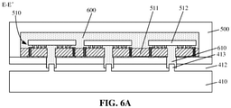
FIG. 1A to FIG. 1C are schematic structural diagrams of an injection moulding process of one specific example of the disclosure; -
FIG. 2A to FIG. 2C are schematic structural diagrams of a base plate of an injection mould of one specific example of the disclosure; -
FIG. 3 is a schematic structural diagram of a base plate of an injection mould of one specific example of the disclosure; -
FIG. 4A to FIG. 4D are schematic structural diagrams of a base plate of an injection mould of one specific example of the disclosure; and -
FIG. 5A to FIG. 6B are schematic structural diagrams of an injection moulding process for a packaged chip in one specific example of the disclosure. - As mentioned in the background, in the related art, a problem that gas cannot be exhausted is prone to occur during injection moulding of a packaged chip made by a flip chip process.
- In order to solve the above-mentioned problem, in one specific example of the disclosure, an injection mould is provided. A base plate of the mould is provided with a groove that can connect with a gas hole of a substrate of the packaged chip, so that gas is exhausted out of the mould from the gas hole and through the groove.
- Referring to
FIG. 1A to FIG. 1C , schematic structural diagrams for injection molding with an injection mold with a groove in one specific example of the disclosure are illustrated.FIG. 1A is a schematic top view;FIG. 1B is a schematic sectional view along a cut line AA' inFIG. 1A ; andFIG. 1C is a schematic sectional view along a cut line BB' inFIG. 1A . - The packaged chip includes a
substrate 110 and achip 111 mounted on thesubstrate 110 by a flip chip process. Specifically, thesubstrate 110 has a front surface and a back surface which are opposite, and thechip 111 is fixed on the front surface of thesubstrate 110. The packaged chip is placed in a cavity of the injection mould, and thesubstrate 110 is provided with agas hole 113. - The injection mould includes a
base plate 101 and acover 102. Thebase plate 101 has agroove 120 inside. Two ends of thegroove 120 are open and connect to the exterior of the injection mould. The packaged chip is placed on thebase plate 101, and thegas hole 113 connects with thegroove 120. During injection of amoulding compound 112, gas is exhausted out of the mould through thegas hole 113 of thesubstrate 110 firstly and thegroove 120 of thebase plate 101 secondly. As compared with a situation where only the gas hole of thesubstrate 101 is formed, the disclosure forms thegroove 120, which connects with thegas hole 113, in thebase plate 101 of the injection mould, which can further enhance the exhaust effect during injection moulding. - However, in the injection moulding process, the edge of the cavity in the mould will be usually filled with the moulding compound first; so that the
chip 111 located at the edge position will be wrapped by the moulding compound first. The moulding compound overflowing from thegas hole 113 of thesubstrate 101 into thegroove 120 may possibly block the two ends of thegroove 120 at the substrate 101 (such as the position of aregion 130 inFIG. 1A ) when the cavity is not filled up by the moulding compound. At this time, thegroove 120 will not achieve a relatively good exhaust effect, and the problem that air cannot be exhausted in the injection moulding process still exists, resulting in formation of a hole between thechip 111 and thesubstrate 110, affecting the reliability of the device. - The inventors further proposed a new mould to improve the above-mentioned problem.
- Specific examples of a new injection mould and an injection moulding method which are provided by the disclosure are described in detail below in combination with the accompanying drawings.
- In one specific implementation mould, the injection mould includes a base plate used to place a packaged chip to be injection moulded. The packaged chip includes a substrate and at least one of the chips fixed on a front surface of the substrate by a flip chip process, and the substrate has a gas hole penetrating through the substrate. Two or more gas ducts that extend in at least two intersected directions and connect with one another are formed in the base plate. Two ends of each one of the gas ducts are open, and at least one of gas ducts is buried into the base plate. The gas duct is provided with a gas outlet used to connect with the gas hole of the substrate.
- Referring to
FIG. 2A to FIG. 2C , schematic structural diagrams of a base plate of an injection mould of one specific example of the disclosure are illustrated.FIG. 2A is a schematic top view of thebase plate 210;FIG. 2B is a schematic sectional view along a cut line CC' inFIG. 2A ; andFIG. 2C is a schematic sectional view along a cut line DD' inFIG. 2A . - The
base plate 210 has afirst gas duct 211 extending in a first direction and asecond gas duct 212 extending in a second direction. In this specific example, the first direction is an X-axis direction, and the second direction is a Y-axis direction. The first direction is perpendicular to the second direction. In other specific examples, the first direction and the second direction can be intersected in other angles. In this specific example, forming 3 gas ducts in each of the first direction and the second direction is taken as an example. In other specific examples, the number of the gas ducts in each direction can be designed according to the structure of the packaged chip to be moulded and an actual need, and there is no limitation here. - The
base plate 210 has two opposite surfaces, i.e., a front surface and a back surface. The packaged chip is applied and placed on the front surface of thebase plate 210. In this specific example, thefirst gas duct 211 is a groove formed on the front surface of thebase plate 210, and thesecond gas duct 212 is a tunnel buried in thebase plate 211. Thesecond gas duct 212 and thefirst gas duct 211 connect with each other at an intersection. Thefirst gas duct 211 and thesecond gas duct 212 connect with each other at the intersection, so that thefirst gas duct 211 and thesecond gas duct 212 form a mesh-type gas duct structure. Gas can also be exhausted in other directions when any one of the intersection is blocked. - The
first gas duct 211 and thesecond gas duct 212 are each provided with a gas outlet. An opening of one end of each gas outlet is located on the front surface of thebase plate 210 and used to connect with the gas hole of the substrate of the packaged chip to be moulded. In this specific example, thefirst gas duct 211 is a groove. The opening of the whole groove can be used as the gas outlet of thefirst gas duct 211. Thesecond gas duct 212 is buried in thebase plate 210, and a gas duct region at a connection between thesecond gas duct 212 and thefirst gas duct 211 is used as the gas outlet of thesecond gas duct 212. In this specific example, the gas outlet of thesecond gas duct 212 is located at the intersection between thesecond gas duct 212 and thefirst gas duct 211. - Optionally, the gas holes of the substrate of the packaged chip to be moulded are arranged in a straight line. When the packaged chip is placed on the surface of the
base plate 210, the extending direction of thefirst gas duct 211 is consistent with the direction in which the gas holes are arranged in the substrate, and each of thefirst gas ducts 211 connects to the gas holes located on the same straight line. When the packaged chip is moulded, a moulding compound enters the first gas duct from the gas hole of the substrate of the chip. Finally, after the injection moulding is completed, and the moulding compound is solidified, a moulding compound strip located on the back surface of the substrate is formed in the first gas duct to close the gas hole connecting with the first gas duct, thereby enhancing the closing effect on the gas hole of the substrate. In this specific example, thefirst gas duct 211 has a width range of 100 µm to 1 mm. Formation of an oversized moulding compound strip on the back surface of the substrate which occupies an excessive area of the back surface of the substrate to affect the circuit distribution on the back surface of the substrate is avoided while satisfying an exhaust requirement. - In other specific examples, gas ducts extending in three or more directions can also be formed to improve the gas exhausting efficiency. In a direction perpendicular to the surface of the base plate, the gas ducts in at least two different extending directions are respectively located at different depths of the base plate.
- In one specific example, the gas ducts extending in various directions are all buried into the base plate, and the gas ducts extending in different directions are buried at different depths and perpendicularly connect with one another at an intersection. A through hole in the intersection is used as the gas outlet of the various gas ducts to connect to the gas holes of the substrate of the packaged chip to be moulded. Therefore, in this case, the number of gas inlet can be set according to the number of the gas holes of the substrate of the packaged chip to be moulded. This quantity can be equal to or greater than the quantity of the gas holes to adapt to different kinds of packaged chips. In one specific example, the gas outlet is a circular hole with a diameter ranging from 100 µm to 1 mm, preferably 200 µm, 300 µm, 400 µm, 500 µm, 600 µm, 700 µm, or 800 µm. In some specific examples, the gas outlet can also be a rectangular hole with a side ranging from 100 µm to 1 mm.
- In this specific example, after the packaged chip is moulded, only a dot-like moulding compound that close the gas hole is formed on the back surface of the substrate of the packaged chip, so that the area that the moulding compound occupies on the back surface of the substrate is reduced, thereby enlarging an area of electric connection structures such as a solder pad and a solder ball formed on the back surface of the substrate.
- In other specific examples, there can also be a gas duct extending in at least one direction which locates on the front surface of the base plate, and is a groove with two ends penetrating through the base plate. The gas duct extending in other directions is buried into the base plate.
- In a direction perpendicular to the extending direction, the cross section of the gas duct can be circular, rectangular, semicircular, elliptical, or of other shapes.
- In the specific example of the disclosure, the extending direction of the gas duct and the number of the extending directions are not limited. Those skilled in the art can design these according to actual needs.
- In order to improve the gas exhausting efficiency, the gas duct can have a relatively large cross-sectional size. A maximum distance between any two points on the edge of the cross section perpendicular to a length direction of the gas duct ranges from 500 µm to 5 mm. When the cross section of the gas duct is circular, the maximum distance is the diameter of the cross section. When the cross section of the gas duct is rectangular, the maximum distance is the maximum side of the cross section. Furthermore, different cross-sectional sizes can also be set according to the depths that the gas ducts are located in the base plate. Preferably, the cross-sectional area of the lower gas duct can be larger than the cross-sectional area of the upper gas duct. In this specific example, the
first gas duct 211 is the groove located on the surface of the base plate and has a rectangular cross section with side range of 500 µm to 2 mm, preferably 800 µm to 1.7 mm. Thesecond gas duct 212 is located below thefirst gas duct 211 and has a circular cross section with a diameter range of 500 µm to 5 mm, preferably 800 µm to 4 µm. The larger the cross-sectional area of the gas duct is, the higher gas exhausting efficiency results. - In this specific example, the
first gas duct 211 and thesecond gas duct 212 are both linear gas ducts. In other specific examples, the gas duct can also be curved, such as thegas duct 301 inFIG. 3 . The shape and extending direction of the various gas ducts can be designed according to the arrangement of the gas hole of the substrate of the chip to be packaged. Any shape and arrangement rule shall fall within the protection scope of the disclosure, and are not listed one by one here. - Referring to
FIG. 4A to FIG. 4D , schematic structural diagrams of a base plate of another specific example of the disclosure are illustrated.FIG. 4A is a schematic top view of a surface of thebase plate 410;FIG. 4B is a schematic sectional diagram along a cut line E-E' inFIG. 4A ;FIG. 4C is a schematic sectional diagram along a cut line F-F' inFIG. 4A ; andFIG. 4D is a schematic sectional diagram along a cut line G-G' inFIG. 4A . - In this specific example, a
first gas duct 411 extending in a first direction (x-axis) is on the surface of thebase plate 410, and asecond gas duct 412 extending in a second direction (y-axis) is inside thebase plate 410. Thefirst gas duct 411 is a groove formed on the front surface of thebase plate 410, and thesecond gas duct 412 is a tunnel buried in thebase plate 410. Thefirst gas duct 411 and thesecond gas duct 412 connect with each other at an intersection. - Particularly, in this specific example, a
step 413 is provided at a position in thesecond gas duct 412 which connects to thefirst gas duct 411. Thestep 413 is connected to the bottom of other positions of thefirst gas duct 411 in an extending direction of thefirst gas duct 411. In this specific example, the surface of thestep 413 is flush with the bottom surface of other positions of thefirst gas duct 411. In other specific examples, the surface of thestep 413 can also be slightly higher than or lower than the bottom surface of thefirst gas duct 411. - Referring to
FIG. 4B , due to the existence of thestep 413 at the connection between thefirst gas duct 411 and thesecond gas duct 412, in an injection moulding process of a chip, when a moulding compound enters thesecond gas duct 412 from thefirst gas duct 411, the flowing path is relatively small; and the moulding compound is easy to break at this position when taking out the packaged chip after the moulding compound is solidified, which is convenient for taking out the packaged chip from the injection mould after the injection moulding. - The injection mould further includes a cover used to cover the base plate to form a cavity with the base plate. The cavity is used to accommodate the packaged chip to be injection moulded. The gas duct of the base plate connects the cavity with the outside of the injection mould. The cover is provided with at least one injection hole used to inject the moulding compound to the cavity. A gas outlet hole can also be formed in the cover and used to connect the cavity to the outside of the injection mould.
- The base plate of the injection mould has the gas ducts extending in multiple directions, and the gas ducts extending in various directions connect to form a mesh-type gas duct structure. In the injection moulding process, when two ends of part of the gas ducts are blocked, gas can still be exhausted through the gas duct in other directions, thereby lowering the risk that gas in an injection moulding cavity cannot be exhausted and improving the reliability of the packaged chip after injection moulding.
- The specific example of the disclosure further provides an injection moulding method. The method performs injection moulding on a packaged chip by using the injection mould provided in the above-mentioned specific example.
- Referring to
FIG. 5A to FIG. 6B , schematic structural diagrams of an injection moulding process for a packaged chip in one specific example of the disclosure are illustrated. - Referring to
FIG. 5A to FIG. 5B , an injection mould is provided. The injection mould includes a base plate 400 and acover 500. The specific structure of the base plate 400 refer toFIG. 4A to FIG. 4D , and details thereof are omitted here. - A packaged
chip 510 to be injection moulded is placed on the front surface of the base plate 400. The packagedchip 510 includes asubstrate 511 and at least one of thechips 512 fixed on the front surface of thesubstrate 511 by a flip chip process. The substrate is provided with agas hole 513. Thecover 500 covers the surface of the base plate 400 to form acavity 520, and the packaged chip is located in thecavity 520. The back surface of thesubstrate 511 is contacted to the surface of thebase plate 410, and thegas hole 513 of thesubstrate 511 of the packagedchip 510 connects with a gas duct of thebase plate 410. The front surface and the back surface of thesubstrate 511 are two opposite surfaces. - The
substrate 511 of the packagedchip 510 is a circuit board on which an electric connection structure such as a circuit and a solder pad is formed.Several chips 512 are packaged on the surfaces by the flip chip process. Thechip 512 is flipped on the surface of thesubstrate 511 and is electrically connected to the electric connection structure on the surface of thesubstrate 511 by a solder bump. The solder bump can be a solder ball, a copper pillar, or other structures. - At least one of the gas holes 513 is formed in a substrate region that each
chip 512 of the packagedchip 510 is located. At least part of the gas holes connects with the gas duct of thebase plate 410 to exhaust air by the gas duct. Preferably, all the gas holes 513 of thesubstrate 511 connect with the gas duct of thebase plate 410 to improve the exhaust efficiency. In this specific example, thegas hole 513 is a circular hole, the size of which is slightly less than or equal to the size of a gas outlet of the gas duct of thebase plate 410. Specifically, the diameter of thegas hole 513 is less than the width of thefirst gas duct 411. In one specific example, the diameter of thegas hole 513 ranges from 800 µm to 0.8 mm, and the width of thefirst gas duct 411 ranges from 100 µm to 1 mm. - In this specific example, the
base plate 410 includes a groove-likefirst gas duct 411 located on the front surface and asecond gas duct 412 buried in thebase plate 410. The gas holes 513 of thesubstrate 511 are arranged in an extending direction of thefirst gas duct 411. The gas holes 513 located on the same straight line connect to the samefirst gas duct 411. - In other specific examples, the gas ducts of the base plate can be all buried in the base plate. The gas outlet of the gas duct, which is a hole, penetrates through to the front surface of the base plate. The
gas hole 513 of thesubstrate 511 connects with at least part of the gas outlets on the front surface of the base plate. - Referring to
FIG. 6A to FIG. 6B , amoulding compound 600 in the state of liquid is injected to thecavity 520 through an injection hole (not shown) in the cover 500 (referring toFIG. 5A to FIG. 5B ). In the injection process, at least part of air in thecavity 520 is exhausted through the gas hole 513 (referring toFIG. 5A to FIG. 5B ) and the gas ducts to the outside of the injection mould. - When the moulding compound in the state of liquid is injected to the
cavity 520, the flow rate is controlled so that gas in thecavity 520 has enough time to be exhausted through the gas duct. Preferably, in some specific examples, the injection moulding pressure intensity in the injection moulding process is controlled to range from 7E6 Pa to 1E7 Pa. - In some specific examples, two or more injection holes can be formed in the
cover 500. The moulding compound can be injected to the cavity through the two or more injection holes to improve the injection efficiency. Thecover 500 can also have a gas outlet hole (not shown). The gas at the upper part of thecavity 520 can be exhausted to the outside through the gas outlet hole in thecover 500, thereby reducing the volume of gas needing to be exhausted from the gas ducts of thebase plate 410. The flow rate of the injection moulding compound can be properly increased to improve the injection moulding efficiency. - After the cavity is filled up with the moulding compound, heat treatment is performed to solidify the
moulding compound 600; and the packagedchip 510 covered with the moulding compound is taken out from the cavity. - In this specific example, in the injection moulding process, the
moulding compound 600 enters thefirst gas duct 411 from the gas hole of thesubstrate 511. The packagedchip 510 is taken out from the mould, carrying the moulding compound formed in thefirst gas duct 411, so that the back surface of thesubstrate 511 has a mouldedstrip 610. The mouldedstrip 610 closes the gas holes located on the same straight line to enhance the closing effect on the gas hole. - In other specific examples, groove-like gas ducts extending in multiple directions can be formed on the front surface of the base plate, so that moulded
strips 610 extending in multiple directions are formed on thesubstrate 511 after the injection moulding is completed. The gas duct distribution positions on the surface of the base plate need to be reasonably set according to the positions of the electric connection structure such as the solder pads formed on the back surface of thesubstrate 511 to avoid the formed mouldedstrip 610 from affecting the connection structure on the back surface of thesubstrate 511. - Referring to
FIG. 6A , onestep 413 is provided at the connection between thefirst gas duct 411 and thesecond gas duct 412, a connection channel between thefirst gas duct 411 and thesecond gas duct 412 is relatively narrow, and the connection intensity of the moulding compound at the connection between thefirst gas duct 411 and thesecond gas duct 412 is relatively low. Therefore, after the injection moulding is completed, in the process of taking out the packagedchip 510, the moulding compound at the connection between thefirst gas duct 411 and thesecond gas duct 412 is easy to break so that it is easy to take out the packagedchip 510. After the packagedchip 510 is taken out, the method further includes the following acts. A solder ball is formed on the surface of the other side of the packagedchip 510, the solder ball is electrically connected to thechip 512 on the front surface of thesubstrate 511 by the electric connection structure at thesubstrate 510; then thesubstrate 510 is cut to form a moulded packaged chip including asingle chip 512. - The above descriptions are only the preferred examples of the disclosure. It should be noted that those skilled in the art can further make several improvements and retouches without departing from the principles of the disclosure. These improvements and retouches shall all fall within the protection scope of the disclosure.
Claims (15)
- An injection mould, comprising,a base plate used to place a packaged chip to be injection moulded, wherein the packaged chip comprises a substrate and at least one of the chips fixed on a front surface of the substrate by a flip chip process, and the substrate has a gas hole penetrating through the substrate;two or more gas ducts that extend in at least two intersected directions and connect with one another are formed in the base plate; two ends of each one of the gas ducts are open, and at least one of the gas ducts is buried into the base plate; and the gas duct is provided with a gas outlet used to connect with the gas hole of the substrate.
- The injection mould according to claim 1, wherein at least one of the two or more gas ducts is located on the front surface of the base plate; the gas duct located on the front surface of the base plate is a groove located on the front surface of the base plate; and the gas ducts buried into the base plate are tunnels located inside the base plate.
- The injection mould according to claim 1, wherein in a direction perpendicular to a surface of the base plate, the gas ducts that extend in at least two different directions are respectively located at different depths in the base plate.
- The injection mould according to claim 1, wherein the gas ducts that extend in at least one of the directions is buried into the base plate.
- The injection mould according to claim 1, wherein the gas outlet is located at the intersection of the different gas ducts, so that the intersected gas ducts connect with one another.
- The injection mould according to claim 1, wherein a maximum distance between any two points on an edge of a cross section perpendicular to a length direction of the gas duct ranges from 500 µm to 5 mm.
- The injection mould according to claim 1, wherein a size of the gas outlet of the gas duct is larger than or equal to a size of the gas hole of the substrate.
- The injection mould according to claim 1, wherein a first gas duct extending in a first direction and a second gas duct extending in a second direction are formed in the base plate; the first gas duct is a groove formed on a surface of the base plate; the second gas duct is a tunnel buried into the base plate; the second gas duct and the first gas duct connect with each other at the intersection.
- The injection mould according to claim 8, wherein a step is provided in the second gas duct at a position connecting to the first gas duct; and the step is connected to a bottom of the first gas duct in an extending direction of the first gas duct.
- The injection mould according to claim 1, wherein the gas holes of the substrate of the packaged chip to be injection moulded are arranged in a straight line; an extending direction of the first gas duct is consistent with a direction in which the gas holes are arranged; and each of the first gas ducts is used to connect to the gas holes on a same straight line.
- The injection mould according to claim 1, further comprising a cover used to cover the base plate to form a cavity with the base plate; the cavity is used to accommodate the packaged chip to be injection moulded; the gas duct of the base plate connect the cavity with the outside of the injection mould; and the cover is provided with at least one injection hole used to inject a moulding compound to the cavity.
- An injection moulding method, comprising:providing the injection mould according to claim 11 and the packaged chip to be injection moulded, the packaged chip comprising the substrate and at least one of the chips fixed on the front surface of the substrate by a flip chip process, and the substrate having the gas hole penetrating through the substrate;placing the packaged chip on the base plate of the injection mould and covering the base plate with the cover to form the cavity, the packaged chip being located in the cavity, a back surface of the substrate being contacted to a surface of the base plate, and the gas hole of the substrate of the packaged chip connecting with the gas duct of the base plate; andinjecting the moulding compound in a state of liquid to the cavity through the injection hole of the cover, at least part of gas in the cavity being exhausted out of the injection mould through the gas hole and the gas duct in the injection process.
- The injection moulding method according to claim 12, wherein the moulding compound is injected to the cavity through two or more injection holes.
- The injection moulding method according to claim 12, wherein at least one of the gas holes is formed in a substrate region on which each one of the packaged chips is located.
- The injection moulding method according to claim 12, further comprising: after the cavity is filled up with the moulding compound in the state of liquid, performing heat treatment to solidify the moulding compound in the state of liquid; and taking out the packaged chip wrapped by a solidified moulding compound from the cavity.
Applications Claiming Priority (2)
| Application Number | Priority Date | Filing Date | Title |
|---|---|---|---|
| CN202010102763.2A CN113276348B (en) | 2020-02-19 | 2020-02-19 | Injection mold and injection molding method |
| PCT/CN2021/075942 WO2021164605A1 (en) | 2020-02-19 | 2021-02-08 | Injection mold and injection molding method |
Publications (3)
| Publication Number | Publication Date |
|---|---|
| EP3950261A1 true EP3950261A1 (en) | 2022-02-09 |
| EP3950261A4 EP3950261A4 (en) | 2022-06-15 |
| EP3950261B1 EP3950261B1 (en) | 2023-11-29 |
Family
ID=77274901
Family Applications (1)
| Application Number | Title | Priority Date | Filing Date |
|---|---|---|---|
| EP21757866.5A Active EP3950261B1 (en) | 2020-02-19 | 2021-02-08 | Injection mold and injection molding method |
Country Status (4)
| Country | Link |
|---|---|
| US (1) | US11820058B2 (en) |
| EP (1) | EP3950261B1 (en) |
| CN (1) | CN113276348B (en) |
| WO (1) | WO2021164605A1 (en) |
Families Citing this family (2)
| Publication number | Priority date | Publication date | Assignee | Title |
|---|---|---|---|---|
| CN113276359B (en) * | 2020-02-19 | 2022-11-08 | 长鑫存储技术有限公司 | Injection mold and injection molding method |
| CN113394118B (en) * | 2020-03-13 | 2022-03-18 | 长鑫存储技术有限公司 | Package structure and method of forming the same |
Family Cites Families (22)
| Publication number | Priority date | Publication date | Assignee | Title |
|---|---|---|---|---|
| US5866442A (en) * | 1997-01-28 | 1999-02-02 | Micron Technology, Inc. | Method and apparatus for filling a gap between spaced layers of a semiconductor |
| US5923959A (en) | 1997-07-23 | 1999-07-13 | Micron Technology, Inc. | Ball grid array (BGA) encapsulation mold |
| US6383846B1 (en) * | 2000-03-20 | 2002-05-07 | Chi-Chih Shen | Method and apparatus for molding a flip chip semiconductor device |
| JP4319759B2 (en) * | 2000-03-21 | 2009-08-26 | アピックヤマダ株式会社 | Resin sealing device and resin sealing method |
| SG107567A1 (en) * | 2001-11-07 | 2004-12-29 | Advanced Systems Automation | Method and apparatus for forming a flip chip semiconductor package and method for producing a substrate for the flip chip semiconductor package |
| CN1291466C (en) * | 2001-12-27 | 2006-12-20 | 威宇科技测试封装有限公司 | Semiconductor packaging method with radiating fin |
| TW584922B (en) * | 2002-07-03 | 2004-04-21 | United Test Ct Inc | Method of manufacturing semiconductor package |
| JP4474113B2 (en) * | 2003-04-07 | 2010-06-02 | 日立化成工業株式会社 | Solid epoxy resin molding material for sealing and semiconductor device |
| CN101347968A (en) * | 2007-07-16 | 2009-01-21 | 汉达精密电子(昆山)有限公司 | Improved exhaust structure |
| JP5067664B2 (en) * | 2008-03-25 | 2012-11-07 | コニカミノルタアドバンストレイヤー株式会社 | Mold for optical element and optical element |
| KR20120062457A (en) * | 2010-12-06 | 2012-06-14 | 삼성전자주식회사 | Print circuit board for semiconductor package improving a solder joint reliablity and semiconductor package having the same |
| JP5723617B2 (en) * | 2011-02-04 | 2015-05-27 | Hoya株式会社 | INJECTION MOLDING DEVICE, MOLD, AND METHOD FOR PRODUCING INJECTION MOLDED PRODUCT |
| KR101902996B1 (en) | 2012-07-09 | 2018-10-01 | 삼성전자주식회사 | Semiconductor package and method of forming the same |
| KR102003279B1 (en) * | 2012-07-17 | 2019-07-25 | 삼성전자 주식회사 | Low die apparatus for semiconductor molding apparatus, semiconductor package and method for fabricating the same |
| CN203254619U (en) * | 2013-03-19 | 2013-10-30 | 吴江凯明塑胶有限公司 | Exhaust structure of die |
| CN204773390U (en) * | 2015-07-14 | 2015-11-18 | 东莞市贝洛橡胶制品有限公司 | Automatic exhaust major diameter cushion rubber spare forming die |
| CN107369655A (en) * | 2017-07-13 | 2017-11-21 | 睿力集成电路有限公司 | A kind of window-type ball grid array package assembling |
| CN207711281U (en) * | 2017-12-08 | 2018-08-10 | 深圳市平进股份有限公司 | A kind of injection mold that hyperfrequency vibrations are smooth with Electric Pulse Treatment precision |
| CN207841976U (en) * | 2017-12-29 | 2018-09-11 | 青岛鑫可佳精密模具有限责任公司 | An a kind of mould four barrel master structure |
| CN208020631U (en) * | 2018-03-13 | 2018-10-30 | 苏州精锐精密机械有限公司 | Injection mold |
| CN108773021A (en) * | 2018-05-08 | 2018-11-09 | 珠海格力精密模具有限公司 | Injection mold and injection moulding process |
| CN109262992B (en) * | 2018-09-26 | 2020-11-20 | 陕西智拓固相增材制造技术有限公司 | Breathable insert processing method and breathable insert |
-
2020
- 2020-02-19 CN CN202010102763.2A patent/CN113276348B/en active Active
-
2021
- 2021-02-08 EP EP21757866.5A patent/EP3950261B1/en active Active
- 2021-02-08 WO PCT/CN2021/075942 patent/WO2021164605A1/en not_active Ceased
- 2021-07-13 US US17/373,930 patent/US11820058B2/en active Active
Also Published As
| Publication number | Publication date |
|---|---|
| CN113276348B (en) | 2023-01-24 |
| WO2021164605A1 (en) | 2021-08-26 |
| EP3950261A4 (en) | 2022-06-15 |
| US11820058B2 (en) | 2023-11-21 |
| CN113276348A (en) | 2021-08-20 |
| EP3950261B1 (en) | 2023-11-29 |
| US20210339443A1 (en) | 2021-11-04 |
Similar Documents
| Publication | Publication Date | Title |
|---|---|---|
| US12186952B2 (en) | Injection mould and injection moulding method | |
| US6521980B1 (en) | Controlling packaging encapsulant leakage | |
| US11820058B2 (en) | Injection mould and injection moulding method | |
| EP0817261A1 (en) | Method for manufacturing plastic package for electronic device having a fully insulated dissipator | |
| JP2008004570A (en) | Resin-sealed semiconductor device manufacturing method, resin-sealed semiconductor device manufacturing apparatus, and resin-sealed semiconductor device | |
| CN211404481U (en) | Package substrate and package structure | |
| EP3933897B1 (en) | Packaging structure and formation method therefor | |
| JP3453210B2 (en) | Molding equipment for resin sealing | |
| CN113284855B (en) | Package substrate and forming method thereof, package structure and forming method thereof | |
| CN100490131C (en) | Ball grid array package structure for preventing glue overflow | |
| US7674657B2 (en) | Method of manufacture of encapsulated package | |
| CN115230080A (en) | SIP imposition Mold and its production method and use method | |
| CN219085963U (en) | Semiconductor package and electronic device | |
| JP2008187143A (en) | Circuit device and manufacturing method thereof | |
| CN101814462B (en) | Manufacturing method and sealing method of semiconductor package | |
| JP2001168123A (en) | Semiconductor device and manufacturing method thereof, semiconductor device manufacturing apparatus, circuit board, and electronic equipment | |
| US20260107825A1 (en) | Mold compound void mitigation | |
| US8212368B2 (en) | Semiconductor package and manufacturing method thereof and encapsulating method thereof | |
| KR20250101773A (en) | Semiconductor device, semiconductor package and printed circuit board | |
| CN100466212C (en) | Semiconductor package and fabrication method thereof | |
| US20240282650A1 (en) | Semiconductor device | |
| JP2010021185A (en) | Semiconductor package substrate and semiconductor package using the same | |
| CN100539108C (en) | Mounting structure and mounting method of electronic components | |
| CN101106112A (en) | Mounting structure of electronic component and mounting method thereof | |
| JP3061114U (en) | Mold resin for semiconductor devices |
Legal Events
| Date | Code | Title | Description |
|---|---|---|---|
| STAA | Information on the status of an ep patent application or granted ep patent |
Free format text: STATUS: THE INTERNATIONAL PUBLICATION HAS BEEN MADE |
|
| PUAI | Public reference made under article 153(3) epc to a published international application that has entered the european phase |
Free format text: ORIGINAL CODE: 0009012 |
|
| STAA | Information on the status of an ep patent application or granted ep patent |
Free format text: STATUS: REQUEST FOR EXAMINATION WAS MADE |
|
| 17P | Request for examination filed |
Effective date: 20211105 |
|
| AK | Designated contracting states |
Kind code of ref document: A1 Designated state(s): AL AT BE BG CH CY CZ DE DK EE ES FI FR GB GR HR HU IE IS IT LI LT LU LV MC MK MT NL NO PL PT RO RS SE SI SK SM TR |
|
| A4 | Supplementary search report drawn up and despatched |
Effective date: 20220517 |
|
| RIC1 | Information provided on ipc code assigned before grant |
Ipc: H01L 21/56 20060101ALI20220511BHEP Ipc: B29C 33/10 20060101ALI20220511BHEP Ipc: B29C 45/34 20060101ALI20220511BHEP Ipc: B29C 45/26 20060101AFI20220511BHEP |
|
| STAA | Information on the status of an ep patent application or granted ep patent |
Free format text: STATUS: EXAMINATION IS IN PROGRESS |
|
| 17Q | First examination report despatched |
Effective date: 20230209 |
|
| DAV | Request for validation of the european patent (deleted) | ||
| DAX | Request for extension of the european patent (deleted) | ||
| GRAP | Despatch of communication of intention to grant a patent |
Free format text: ORIGINAL CODE: EPIDOSNIGR1 |
|
| STAA | Information on the status of an ep patent application or granted ep patent |
Free format text: STATUS: GRANT OF PATENT IS INTENDED |
|
| INTG | Intention to grant announced |
Effective date: 20230622 |
|
| P01 | Opt-out of the competence of the unified patent court (upc) registered |
Effective date: 20230822 |
|
| GRAS | Grant fee paid |
Free format text: ORIGINAL CODE: EPIDOSNIGR3 |
|
| GRAA | (expected) grant |
Free format text: ORIGINAL CODE: 0009210 |
|
| STAA | Information on the status of an ep patent application or granted ep patent |
Free format text: STATUS: THE PATENT HAS BEEN GRANTED |
|
| AK | Designated contracting states |
Kind code of ref document: B1 Designated state(s): AL AT BE BG CH CY CZ DE DK EE ES FI FR GB GR HR HU IE IS IT LI LT LU LV MC MK MT NL NO PL PT RO RS SE SI SK SM TR |
|
| REG | Reference to a national code |
Ref country code: GB Ref legal event code: FG4D |
|
| REG | Reference to a national code |
Ref country code: CH Ref legal event code: EP |
|
| REG | Reference to a national code |
Ref country code: DE Ref legal event code: R096 Ref document number: 602021007342 Country of ref document: DE |
|
| REG | Reference to a national code |
Ref country code: IE Ref legal event code: FG4D |
|
| REG | Reference to a national code |
Ref country code: LT Ref legal event code: MG9D |
|
| REG | Reference to a national code |
Ref country code: NL Ref legal event code: MP Effective date: 20231129 |
|
| PG25 | Lapsed in a contracting state [announced via postgrant information from national office to epo] |
Ref country code: GR Free format text: LAPSE BECAUSE OF FAILURE TO SUBMIT A TRANSLATION OF THE DESCRIPTION OR TO PAY THE FEE WITHIN THE PRESCRIBED TIME-LIMIT Effective date: 20240301 |
|
| PG25 | Lapsed in a contracting state [announced via postgrant information from national office to epo] |
Ref country code: IS Free format text: LAPSE BECAUSE OF FAILURE TO SUBMIT A TRANSLATION OF THE DESCRIPTION OR TO PAY THE FEE WITHIN THE PRESCRIBED TIME-LIMIT Effective date: 20240329 |
|
| PG25 | Lapsed in a contracting state [announced via postgrant information from national office to epo] |
Ref country code: LT Free format text: LAPSE BECAUSE OF FAILURE TO SUBMIT A TRANSLATION OF THE DESCRIPTION OR TO PAY THE FEE WITHIN THE PRESCRIBED TIME-LIMIT Effective date: 20231129 |
|
| PG25 | Lapsed in a contracting state [announced via postgrant information from national office to epo] |
Ref country code: ES Free format text: LAPSE BECAUSE OF FAILURE TO SUBMIT A TRANSLATION OF THE DESCRIPTION OR TO PAY THE FEE WITHIN THE PRESCRIBED TIME-LIMIT Effective date: 20231129 |
|
| PG25 | Lapsed in a contracting state [announced via postgrant information from national office to epo] |
Ref country code: LT Free format text: LAPSE BECAUSE OF FAILURE TO SUBMIT A TRANSLATION OF THE DESCRIPTION OR TO PAY THE FEE WITHIN THE PRESCRIBED TIME-LIMIT Effective date: 20231129 Ref country code: IS Free format text: LAPSE BECAUSE OF FAILURE TO SUBMIT A TRANSLATION OF THE DESCRIPTION OR TO PAY THE FEE WITHIN THE PRESCRIBED TIME-LIMIT Effective date: 20240329 Ref country code: GR Free format text: LAPSE BECAUSE OF FAILURE TO SUBMIT A TRANSLATION OF THE DESCRIPTION OR TO PAY THE FEE WITHIN THE PRESCRIBED TIME-LIMIT Effective date: 20240301 Ref country code: ES Free format text: LAPSE BECAUSE OF FAILURE TO SUBMIT A TRANSLATION OF THE DESCRIPTION OR TO PAY THE FEE WITHIN THE PRESCRIBED TIME-LIMIT Effective date: 20231129 Ref country code: BG Free format text: LAPSE BECAUSE OF FAILURE TO SUBMIT A TRANSLATION OF THE DESCRIPTION OR TO PAY THE FEE WITHIN THE PRESCRIBED TIME-LIMIT Effective date: 20240229 |
|
| REG | Reference to a national code |
Ref country code: AT Ref legal event code: MK05 Ref document number: 1635685 Country of ref document: AT Kind code of ref document: T Effective date: 20231129 |
|
| PG25 | Lapsed in a contracting state [announced via postgrant information from national office to epo] |
Ref country code: NL Free format text: LAPSE BECAUSE OF FAILURE TO SUBMIT A TRANSLATION OF THE DESCRIPTION OR TO PAY THE FEE WITHIN THE PRESCRIBED TIME-LIMIT Effective date: 20231129 |
|
| PG25 | Lapsed in a contracting state [announced via postgrant information from national office to epo] |
Ref country code: SE Free format text: LAPSE BECAUSE OF FAILURE TO SUBMIT A TRANSLATION OF THE DESCRIPTION OR TO PAY THE FEE WITHIN THE PRESCRIBED TIME-LIMIT Effective date: 20231129 Ref country code: RS Free format text: LAPSE BECAUSE OF FAILURE TO SUBMIT A TRANSLATION OF THE DESCRIPTION OR TO PAY THE FEE WITHIN THE PRESCRIBED TIME-LIMIT Effective date: 20231129 Ref country code: PL Free format text: LAPSE BECAUSE OF FAILURE TO SUBMIT A TRANSLATION OF THE DESCRIPTION OR TO PAY THE FEE WITHIN THE PRESCRIBED TIME-LIMIT Effective date: 20231129 Ref country code: NO Free format text: LAPSE BECAUSE OF FAILURE TO SUBMIT A TRANSLATION OF THE DESCRIPTION OR TO PAY THE FEE WITHIN THE PRESCRIBED TIME-LIMIT Effective date: 20240229 Ref country code: NL Free format text: LAPSE BECAUSE OF FAILURE TO SUBMIT A TRANSLATION OF THE DESCRIPTION OR TO PAY THE FEE WITHIN THE PRESCRIBED TIME-LIMIT Effective date: 20231129 Ref country code: LV Free format text: LAPSE BECAUSE OF FAILURE TO SUBMIT A TRANSLATION OF THE DESCRIPTION OR TO PAY THE FEE WITHIN THE PRESCRIBED TIME-LIMIT Effective date: 20231129 Ref country code: HR Free format text: LAPSE BECAUSE OF FAILURE TO SUBMIT A TRANSLATION OF THE DESCRIPTION OR TO PAY THE FEE WITHIN THE PRESCRIBED TIME-LIMIT Effective date: 20231129 |
|
| PG25 | Lapsed in a contracting state [announced via postgrant information from national office to epo] |
Ref country code: DK Free format text: LAPSE BECAUSE OF FAILURE TO SUBMIT A TRANSLATION OF THE DESCRIPTION OR TO PAY THE FEE WITHIN THE PRESCRIBED TIME-LIMIT Effective date: 20231129 |
|
| PG25 | Lapsed in a contracting state [announced via postgrant information from national office to epo] |
Ref country code: CZ Free format text: LAPSE BECAUSE OF FAILURE TO SUBMIT A TRANSLATION OF THE DESCRIPTION OR TO PAY THE FEE WITHIN THE PRESCRIBED TIME-LIMIT Effective date: 20231129 Ref country code: AT Free format text: LAPSE BECAUSE OF FAILURE TO SUBMIT A TRANSLATION OF THE DESCRIPTION OR TO PAY THE FEE WITHIN THE PRESCRIBED TIME-LIMIT Effective date: 20231129 |
|
| PG25 | Lapsed in a contracting state [announced via postgrant information from national office to epo] |
Ref country code: SK Free format text: LAPSE BECAUSE OF FAILURE TO SUBMIT A TRANSLATION OF THE DESCRIPTION OR TO PAY THE FEE WITHIN THE PRESCRIBED TIME-LIMIT Effective date: 20231129 |
|
| PG25 | Lapsed in a contracting state [announced via postgrant information from national office to epo] |
Ref country code: SM Free format text: LAPSE BECAUSE OF FAILURE TO SUBMIT A TRANSLATION OF THE DESCRIPTION OR TO PAY THE FEE WITHIN THE PRESCRIBED TIME-LIMIT Effective date: 20231129 Ref country code: SK Free format text: LAPSE BECAUSE OF FAILURE TO SUBMIT A TRANSLATION OF THE DESCRIPTION OR TO PAY THE FEE WITHIN THE PRESCRIBED TIME-LIMIT Effective date: 20231129 Ref country code: RO Free format text: LAPSE BECAUSE OF FAILURE TO SUBMIT A TRANSLATION OF THE DESCRIPTION OR TO PAY THE FEE WITHIN THE PRESCRIBED TIME-LIMIT Effective date: 20231129 Ref country code: IT Free format text: LAPSE BECAUSE OF FAILURE TO SUBMIT A TRANSLATION OF THE DESCRIPTION OR TO PAY THE FEE WITHIN THE PRESCRIBED TIME-LIMIT Effective date: 20231129 Ref country code: EE Free format text: LAPSE BECAUSE OF FAILURE TO SUBMIT A TRANSLATION OF THE DESCRIPTION OR TO PAY THE FEE WITHIN THE PRESCRIBED TIME-LIMIT Effective date: 20231129 Ref country code: DK Free format text: LAPSE BECAUSE OF FAILURE TO SUBMIT A TRANSLATION OF THE DESCRIPTION OR TO PAY THE FEE WITHIN THE PRESCRIBED TIME-LIMIT Effective date: 20231129 Ref country code: CZ Free format text: LAPSE BECAUSE OF FAILURE TO SUBMIT A TRANSLATION OF THE DESCRIPTION OR TO PAY THE FEE WITHIN THE PRESCRIBED TIME-LIMIT Effective date: 20231129 Ref country code: AT Free format text: LAPSE BECAUSE OF FAILURE TO SUBMIT A TRANSLATION OF THE DESCRIPTION OR TO PAY THE FEE WITHIN THE PRESCRIBED TIME-LIMIT Effective date: 20231129 |
|
| PG25 | Lapsed in a contracting state [announced via postgrant information from national office to epo] |
Ref country code: PT Free format text: LAPSE BECAUSE OF FAILURE TO SUBMIT A TRANSLATION OF THE DESCRIPTION OR TO PAY THE FEE WITHIN THE PRESCRIBED TIME-LIMIT Effective date: 20240401 |
|
| PG25 | Lapsed in a contracting state [announced via postgrant information from national office to epo] |
Ref country code: PT Free format text: LAPSE BECAUSE OF FAILURE TO SUBMIT A TRANSLATION OF THE DESCRIPTION OR TO PAY THE FEE WITHIN THE PRESCRIBED TIME-LIMIT Effective date: 20240401 |
|
| REG | Reference to a national code |
Ref country code: DE Ref legal event code: R097 Ref document number: 602021007342 Country of ref document: DE |
|
| PG25 | Lapsed in a contracting state [announced via postgrant information from national office to epo] |
Ref country code: MC Free format text: LAPSE BECAUSE OF FAILURE TO SUBMIT A TRANSLATION OF THE DESCRIPTION OR TO PAY THE FEE WITHIN THE PRESCRIBED TIME-LIMIT Effective date: 20231129 |
|
| REG | Reference to a national code |
Ref country code: CH Ref legal event code: PL |
|
| PLBE | No opposition filed within time limit |
Free format text: ORIGINAL CODE: 0009261 |
|
| STAA | Information on the status of an ep patent application or granted ep patent |
Free format text: STATUS: NO OPPOSITION FILED WITHIN TIME LIMIT |
|
| PG25 | Lapsed in a contracting state [announced via postgrant information from national office to epo] |
Ref country code: LU Free format text: LAPSE BECAUSE OF NON-PAYMENT OF DUE FEES Effective date: 20240208 |
|
| PG25 | Lapsed in a contracting state [announced via postgrant information from national office to epo] |
Ref country code: CH Free format text: LAPSE BECAUSE OF NON-PAYMENT OF DUE FEES Effective date: 20240229 |
|
| PG25 | Lapsed in a contracting state [announced via postgrant information from national office to epo] |
Ref country code: SI Free format text: LAPSE BECAUSE OF FAILURE TO SUBMIT A TRANSLATION OF THE DESCRIPTION OR TO PAY THE FEE WITHIN THE PRESCRIBED TIME-LIMIT Effective date: 20231129 |
|
| PG25 | Lapsed in a contracting state [announced via postgrant information from national office to epo] |
Ref country code: SI Free format text: LAPSE BECAUSE OF FAILURE TO SUBMIT A TRANSLATION OF THE DESCRIPTION OR TO PAY THE FEE WITHIN THE PRESCRIBED TIME-LIMIT Effective date: 20231129 Ref country code: LU Free format text: LAPSE BECAUSE OF NON-PAYMENT OF DUE FEES Effective date: 20240208 Ref country code: CH Free format text: LAPSE BECAUSE OF NON-PAYMENT OF DUE FEES Effective date: 20240229 |
|
| 26N | No opposition filed |
Effective date: 20240830 |
|
| REG | Reference to a national code |
Ref country code: BE Ref legal event code: MM Effective date: 20240229 |
|
| PG25 | Lapsed in a contracting state [announced via postgrant information from national office to epo] |
Ref country code: BE Free format text: LAPSE BECAUSE OF NON-PAYMENT OF DUE FEES Effective date: 20240229 |
|
| PG25 | Lapsed in a contracting state [announced via postgrant information from national office to epo] |
Ref country code: FR Free format text: LAPSE BECAUSE OF NON-PAYMENT OF DUE FEES Effective date: 20240229 |
|
| PG25 | Lapsed in a contracting state [announced via postgrant information from national office to epo] |
Ref country code: IE Free format text: LAPSE BECAUSE OF NON-PAYMENT OF DUE FEES Effective date: 20240208 |
|
| PG25 | Lapsed in a contracting state [announced via postgrant information from national office to epo] |
Ref country code: IE Free format text: LAPSE BECAUSE OF NON-PAYMENT OF DUE FEES Effective date: 20240208 Ref country code: FR Free format text: LAPSE BECAUSE OF NON-PAYMENT OF DUE FEES Effective date: 20240229 Ref country code: BE Free format text: LAPSE BECAUSE OF NON-PAYMENT OF DUE FEES Effective date: 20240229 |
|
| PG25 | Lapsed in a contracting state [announced via postgrant information from national office to epo] |
Ref country code: CY Free format text: LAPSE BECAUSE OF FAILURE TO SUBMIT A TRANSLATION OF THE DESCRIPTION OR TO PAY THE FEE WITHIN THE PRESCRIBED TIME-LIMIT; INVALID AB INITIO Effective date: 20210208 |
|
| PG25 | Lapsed in a contracting state [announced via postgrant information from national office to epo] |
Ref country code: HU Free format text: LAPSE BECAUSE OF FAILURE TO SUBMIT A TRANSLATION OF THE DESCRIPTION OR TO PAY THE FEE WITHIN THE PRESCRIBED TIME-LIMIT; INVALID AB INITIO Effective date: 20210208 |
|
| PG25 | Lapsed in a contracting state [announced via postgrant information from national office to epo] |
Ref country code: FI Free format text: LAPSE BECAUSE OF FAILURE TO SUBMIT A TRANSLATION OF THE DESCRIPTION OR TO PAY THE FEE WITHIN THE PRESCRIBED TIME-LIMIT Effective date: 20231129 |
|
| GBPC | Gb: european patent ceased through non-payment of renewal fee |
Effective date: 20250208 |
|
| PG25 | Lapsed in a contracting state [announced via postgrant information from national office to epo] |
Ref country code: TR Free format text: LAPSE BECAUSE OF FAILURE TO SUBMIT A TRANSLATION OF THE DESCRIPTION OR TO PAY THE FEE WITHIN THE PRESCRIBED TIME-LIMIT Effective date: 20231129 |
|
| PG25 | Lapsed in a contracting state [announced via postgrant information from national office to epo] |
Ref country code: GB Free format text: LAPSE BECAUSE OF NON-PAYMENT OF DUE FEES Effective date: 20250208 |
|
| PGFP | Annual fee paid to national office [announced via postgrant information from national office to epo] |
Ref country code: DE Payment date: 20260218 Year of fee payment: 6 |