EP3945592B1 - Anzeigetafel und elektronische vorrichtung damit - Google Patents
Anzeigetafel und elektronische vorrichtung damit Download PDFInfo
- Publication number
- EP3945592B1 EP3945592B1 EP21187244.5A EP21187244A EP3945592B1 EP 3945592 B1 EP3945592 B1 EP 3945592B1 EP 21187244 A EP21187244 A EP 21187244A EP 3945592 B1 EP3945592 B1 EP 3945592B1
- Authority
- EP
- European Patent Office
- Prior art keywords
- layer
- partition
- opening
- organic
- display panel
- Prior art date
- Legal status (The legal status is an assumption and is not a legal conclusion. Google has not performed a legal analysis and makes no representation as to the accuracy of the status listed.)
- Active
Links
Images







Classifications
-
- H—ELECTRICITY
- H10—SEMICONDUCTOR DEVICES; ELECTRIC SOLID-STATE DEVICES NOT OTHERWISE PROVIDED FOR
- H10K—ORGANIC ELECTRIC SOLID-STATE DEVICES
- H10K59/00—Integrated devices, or assemblies of multiple devices, comprising at least one organic light-emitting element covered by group H10K50/00
- H10K59/10—OLED displays
- H10K59/12—Active-matrix OLED [AMOLED] displays
- H10K59/122—Pixel-defining structures or layers, e.g. banks
-
- H—ELECTRICITY
- H10—SEMICONDUCTOR DEVICES; ELECTRIC SOLID-STATE DEVICES NOT OTHERWISE PROVIDED FOR
- H10K—ORGANIC ELECTRIC SOLID-STATE DEVICES
- H10K50/00—Organic light-emitting devices
- H10K50/80—Constructional details
- H10K50/84—Passivation; Containers; Encapsulations
- H10K50/844—Encapsulations
- H10K50/8445—Encapsulations multilayered coatings having a repetitive structure, e.g. having multiple organic-inorganic bilayers
-
- H—ELECTRICITY
- H10—SEMICONDUCTOR DEVICES; ELECTRIC SOLID-STATE DEVICES NOT OTHERWISE PROVIDED FOR
- H10K—ORGANIC ELECTRIC SOLID-STATE DEVICES
- H10K50/00—Organic light-emitting devices
- H10K50/10—OLEDs or polymer light-emitting diodes [PLED]
-
- H—ELECTRICITY
- H10—SEMICONDUCTOR DEVICES; ELECTRIC SOLID-STATE DEVICES NOT OTHERWISE PROVIDED FOR
- H10K—ORGANIC ELECTRIC SOLID-STATE DEVICES
- H10K50/00—Organic light-emitting devices
- H10K50/10—OLEDs or polymer light-emitting diodes [PLED]
- H10K50/14—Carrier transporting layers
- H10K50/15—Hole transporting layers
-
- H—ELECTRICITY
- H10—SEMICONDUCTOR DEVICES; ELECTRIC SOLID-STATE DEVICES NOT OTHERWISE PROVIDED FOR
- H10K—ORGANIC ELECTRIC SOLID-STATE DEVICES
- H10K50/00—Organic light-emitting devices
- H10K50/10—OLEDs or polymer light-emitting diodes [PLED]
- H10K50/14—Carrier transporting layers
- H10K50/16—Electron transporting layers
-
- H—ELECTRICITY
- H10—SEMICONDUCTOR DEVICES; ELECTRIC SOLID-STATE DEVICES NOT OTHERWISE PROVIDED FOR
- H10K—ORGANIC ELECTRIC SOLID-STATE DEVICES
- H10K50/00—Organic light-emitting devices
- H10K50/10—OLEDs or polymer light-emitting diodes [PLED]
- H10K50/17—Carrier injection layers
- H10K50/171—Electron injection layers
-
- H—ELECTRICITY
- H10—SEMICONDUCTOR DEVICES; ELECTRIC SOLID-STATE DEVICES NOT OTHERWISE PROVIDED FOR
- H10K—ORGANIC ELECTRIC SOLID-STATE DEVICES
- H10K50/00—Organic light-emitting devices
- H10K50/80—Constructional details
- H10K50/84—Passivation; Containers; Encapsulations
- H10K50/844—Encapsulations
-
- H—ELECTRICITY
- H10—SEMICONDUCTOR DEVICES; ELECTRIC SOLID-STATE DEVICES NOT OTHERWISE PROVIDED FOR
- H10K—ORGANIC ELECTRIC SOLID-STATE DEVICES
- H10K59/00—Integrated devices, or assemblies of multiple devices, comprising at least one organic light-emitting element covered by group H10K50/00
- H10K59/10—OLED displays
-
- H—ELECTRICITY
- H10—SEMICONDUCTOR DEVICES; ELECTRIC SOLID-STATE DEVICES NOT OTHERWISE PROVIDED FOR
- H10K—ORGANIC ELECTRIC SOLID-STATE DEVICES
- H10K59/00—Integrated devices, or assemblies of multiple devices, comprising at least one organic light-emitting element covered by group H10K50/00
- H10K59/10—OLED displays
- H10K59/12—Active-matrix OLED [AMOLED] displays
-
- H—ELECTRICITY
- H10—SEMICONDUCTOR DEVICES; ELECTRIC SOLID-STATE DEVICES NOT OTHERWISE PROVIDED FOR
- H10K—ORGANIC ELECTRIC SOLID-STATE DEVICES
- H10K59/00—Integrated devices, or assemblies of multiple devices, comprising at least one organic light-emitting element covered by group H10K50/00
- H10K59/10—OLED displays
- H10K59/12—Active-matrix OLED [AMOLED] displays
- H10K59/124—Insulating layers formed between TFT elements and OLED elements
-
- H—ELECTRICITY
- H10—SEMICONDUCTOR DEVICES; ELECTRIC SOLID-STATE DEVICES NOT OTHERWISE PROVIDED FOR
- H10K—ORGANIC ELECTRIC SOLID-STATE DEVICES
- H10K59/00—Integrated devices, or assemblies of multiple devices, comprising at least one organic light-emitting element covered by group H10K50/00
- H10K59/10—OLED displays
- H10K59/12—Active-matrix OLED [AMOLED] displays
- H10K59/131—Interconnections, e.g. wiring lines or terminals
-
- H—ELECTRICITY
- H10—SEMICONDUCTOR DEVICES; ELECTRIC SOLID-STATE DEVICES NOT OTHERWISE PROVIDED FOR
- H10K—ORGANIC ELECTRIC SOLID-STATE DEVICES
- H10K59/00—Integrated devices, or assemblies of multiple devices, comprising at least one organic light-emitting element covered by group H10K50/00
- H10K59/60—OLEDs integrated with inorganic light-sensitive elements, e.g. with inorganic solar cells or inorganic photodiodes
- H10K59/65—OLEDs integrated with inorganic image sensors
-
- H—ELECTRICITY
- H10—SEMICONDUCTOR DEVICES; ELECTRIC SOLID-STATE DEVICES NOT OTHERWISE PROVIDED FOR
- H10K—ORGANIC ELECTRIC SOLID-STATE DEVICES
- H10K59/00—Integrated devices, or assemblies of multiple devices, comprising at least one organic light-emitting element covered by group H10K50/00
- H10K59/80—Constructional details
- H10K59/805—Electrodes
- H10K59/8052—Cathodes
- H10K59/80521—Cathodes characterised by their shape
-
- H—ELECTRICITY
- H10—SEMICONDUCTOR DEVICES; ELECTRIC SOLID-STATE DEVICES NOT OTHERWISE PROVIDED FOR
- H10K—ORGANIC ELECTRIC SOLID-STATE DEVICES
- H10K59/00—Integrated devices, or assemblies of multiple devices, comprising at least one organic light-emitting element covered by group H10K50/00
- H10K59/80—Constructional details
- H10K59/87—Passivation; Containers; Encapsulations
- H10K59/873—Encapsulations
-
- H—ELECTRICITY
- H10—SEMICONDUCTOR DEVICES; ELECTRIC SOLID-STATE DEVICES NOT OTHERWISE PROVIDED FOR
- H10K—ORGANIC ELECTRIC SOLID-STATE DEVICES
- H10K2102/00—Constructional details relating to the organic devices covered by this subclass
- H10K2102/301—Details of OLEDs
- H10K2102/351—Thickness
-
- H—ELECTRICITY
- H10—SEMICONDUCTOR DEVICES; ELECTRIC SOLID-STATE DEVICES NOT OTHERWISE PROVIDED FOR
- H10K—ORGANIC ELECTRIC SOLID-STATE DEVICES
- H10K59/00—Integrated devices, or assemblies of multiple devices, comprising at least one organic light-emitting element covered by group H10K50/00
- H10K59/40—OLEDs integrated with touch screens
-
- H—ELECTRICITY
- H10—SEMICONDUCTOR DEVICES; ELECTRIC SOLID-STATE DEVICES NOT OTHERWISE PROVIDED FOR
- H10K—ORGANIC ELECTRIC SOLID-STATE DEVICES
- H10K59/00—Integrated devices, or assemblies of multiple devices, comprising at least one organic light-emitting element covered by group H10K50/00
- H10K59/80—Constructional details
- H10K59/87—Passivation; Containers; Encapsulations
- H10K59/873—Encapsulations
- H10K59/8731—Encapsulations multilayered coatings having a repetitive structure, e.g. having multiple organic-inorganic bilayers
Definitions
- the display panel may further include a structure arranged on the organic insulating layer and including a plurality of protrusions and a concave valley between the plurality of protrusions, wherein a portion of the organic encapsulation layer may be in the concave valley.
- the display panel may further include a planarization insulating layer arranged on the second inorganic encapsulation layer to overlap a portion of the organic encapsulation layer and the first partition and including an organic insulating material.
- the component may include a sensor or a camera.
- a layer, region, or component when a layer, region, or component is referred to as being connected to another layer, region, or component, it may be directly or indirectly connected to the other layer, region, or component. That is, for example, intervening layers, regions, or components may be present.
- intervening layers, regions, or components may be present.
- a layer, region, or component when referred to as being “electrically connected to” another layer, region, or component, it may be “directly electrically connected to" the other layer, region, or component or may be “indirectly electrically connected to" the other layer, region, or component with one or more intervening layers, regions, or components therebetween.
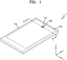
- the electronic apparatus 1 may be formed in a rectangular shape in a plan view.
- the electronic apparatus 1 may have a rectangular planar shape having a short side in the x direction and a long side in the y direction as illustrated in FIG. 1 .
- An edge where the short side in the x direction and the long side in the y direction meet each other may be formed in a round shape having a certain curvature or may be formed in a right-angle shape.
- the planar shape of the electronic apparatus 1 is not limited to a rectangular shape and may be any other polygonal shape, an elliptical shape, or an irregular shape.
- the display element layer 20 may include display elements that emit light to display images.
- the display elements may each include a light emitting diode, for example, an organic light emitting diode including an organic emission layer.
- the light emitting diode may be an inorganic light emitting diode including an inorganic material.
- the inorganic light emitting diode may include a PN diode including inorganic semiconductor-based materials. When a voltage is applied to a PN junction diode in a forward direction, holes and electrons may be injected thereinto and energy generated by recombination of the holes and electrons may be converted into light energy to emit light of a certain color.
- the inorganic light emitting diode described above may have a width of several to several hundred micrometers or a width of several to several hundred nanometers, and according to some embodiments, the inorganic light emitting diode may be referred to as a micro LED or nano LED.
- the optical functional layer 50 may include an anti-reflection layer.
- the anti-reflection layer may be configured to reduce the reflectance of light (external light) incident from the outside through the cover window 60 toward the display panel 10.
- the anti-reflection layer may include a phase retarder and a polarizer.
- the anti-reflection layer may include a black matrix and color filters.
- the color filters may be arranged considering the color of light emitted from each of the light emitting diodes of the display element layer 20.
- the anti-reflection layer may include a destructive interference structure.
- the destructive interference structure may include a first reflection layer and a second reflection layer arranged on different layers. First reflected light and second reflected light respectively reflected by the first reflection layer and the second reflection layer may destructively interfere with each other, and thus the reflectance of external light may be reduced.
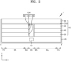
- the display panel 10 may include an opening 10H corresponding to the opening area OA of the electronic apparatus 1.
- FIG. 2 illustrates that the display element layer 20, the input sensing layer 40, and the optical functional layer 50 respectively include first to third openings 20H, 40H, and 50H and the first to third openings 20H, 40H, and 50H overlapping each other form the opening 10H of the display panel 10.
- the opening area OA may be a type of component area (e.g., sensor area, camera area, or speaker area) in which the component 70 for adding various functions to the electronic apparatus 1 is located.
- component area e.g., sensor area, camera area, or speaker area
- FIG. 3 is a plan view schematically illustrating a display panel according to some embodiments
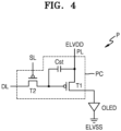
- FIG. 4 illustrates an equivalent circuit connected to any one light emitting diode of a display panel according to some embodiments.
- the first thin film transistor T1 may be connected to the driving voltage line PL and the storage capacitor Cst and may be configured to control a driving current flowing from the driving voltage line PL through the organic light emitting diode OLED in response to a voltage value stored in the storage capacitor Cst.
- the organic light emitting diode OLED may emit light with a certain brightness according to the driving current.
- An opposite electrode (e.g., a cathode) of the organic light emitting diode OLED may be supplied with a second power voltage ELVSS.
- the intermediate area MA may surround the opening area OA.
- the intermediate area MA may be an area in which a display element such as an organic light emitting diode emitting light is not arranged, and signal lines for providing signals to pixels P arranged around the opening area OA may pass through the intermediate area MA.
- data lines DL and/or scan lines SL may intersect the display area DA along the y direction and/or the x direction, while some of the data lines DL and/or the scan lines SL may bypass in the intermediate area MA along the edge of the opening 10H of the display panel 10.
- FIG. 6 is a cross-sectional view schematically illustrating a display panel according to some embodiments, corresponding to a cross-section thereof taken along the line V-V' of FIG. 5
- FIG. 7A is an enlarged cross-sectional view of region VII of FIG. 6
- FIG. 7B is a plan view illustrating the relative positions of partitions, protrusions, and valleys of the display panel of FIG. 6
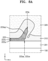
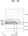
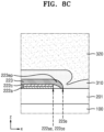
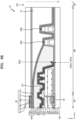
- FIG. 8A to 8C are enlarged cross-sectional views of region VIII of FIG. 6 .
- the optical functional layer 50 see FIG. 2
- the cover window 60 see FIG. 2
- the substrate 100 may include glass material or polymer resin.
- the polymer resin may include polyether sulfone, polyacrylate, polyether imide, polyethylene naphthalate, polyethylene terephthalate, polyphenylene sulfide, polyarylate, polyimide, polycarbonate, and/or cellulose acetate propionate.
- the substrate 100 including the polymer resin may be flexible, rollable, or bendable.
- the substrate 100 may have a multilayer structure including an inorganic insulating layer and a layer including the above polymer resin.
- a pixel electrode 221 may be arranged on the pixel circuit PC, and the pixel electrode 221 may be electrically connected to the pixel circuit PC.
- a contact metal layer CM may be located between the thin film transistor TFT and the pixel electrode 221.
- the contact metal layer CM may be connected to the thin film transistor TFT through a contact hole formed in the first organic insulating layer 209, and the pixel electrode 221 may be arranged on a second organic insulating layer 211 and connected to the contact metal layer CM through a contact hole formed in the second organic insulating layer 211.
- a spacer 217 may be formed on the upper insulating layer 215.
- the spacer 217 may include an organic insulating material.
- the spacer 217 may include the same material as the upper insulating layer 215 and may be formed together in the same mask process as the upper insulating layer 215.
- the second functional layer 222c may include a single layer or a multiple layer.
- the second functional layer 222c may include an electron transport layer (ETL) and/or an electron injection layer (EIL).
- ETL electron transport layer
- EIL electron injection layer
- the emission layer 222b of the intermediate layer 222 may be arranged for each pixel electrode 221 in the display area DA, while the first functional layer 222a and/or the second functional layer 222c may be formed to entirely cover the display area DA.
- Each of the first functional layer 222a and the second functional layer 222c may be a common layer and may cover a plurality of pixel electrodes 221.
- the first inorganic encapsulation layer 310 and the second inorganic encapsulation layer 330 may include one or more inorganic materials among aluminium oxide, titanium oxide, tantalum oxide, hafnium oxide, zinc oxide, silicon oxide, silicon nitride, and silicon oxynitride.
- the first inorganic encapsulation layer 310 and the second inorganic encapsulation layer 330 may include a single layer or a multiple layer including the above material.
- the organic encapsulation layer 320 may include a polymer-based material.
- the polymer-based material may include polymethyl methacrylate, acrylic resin such as polyacrylic acid, epoxy resin, polyimide, polyethylene, or the like. According to some embodiments, the organic encapsulation layer 320 may include an acrylate polymer.
- the first inorganic encapsulation layer 310 and the second inorganic encapsulation layer 330 may have different materials.
- the first inorganic encapsulation layer 310 may include silicon oxynitride
- the second inorganic encapsulation layer 330 may include silicon nitride.
- the first inorganic encapsulation layer 310 and the second inorganic encapsulation layer 330 may have different thicknesses. The thickness of the first inorganic encapsulation layer 310 may be greater than the thickness of the second inorganic encapsulation layer 330.
- the thickness of the second inorganic encapsulation layer 330 may be greater than the thickness of the first inorganic encapsulation layer 310, or the first inorganic encapsulation layer 310 and the second inorganic encapsulation layer 330 may have the same thickness.
- An input sensing layer 40 may be arranged on the thin film encapsulation layer 300.
- the input sensing layer 40 may include first insulating layers 41a and 41b, a first conductive layer CML1, a second insulating layer 43, a second conductive layer CML2, and a third insulating layer 45.
- the first insulating layers 41a and 41b may include a first sub insulating layer 41a and a second sub insulating layer 41b.
- the first sub insulating layer 41a and the second sub insulating layer 41b may include an inorganic insulating material such as silicon oxide, silicon nitride, or silicon oxynitride.
- the first conductive layer CML1 and the second conductive layer CML2 may each include a conductive material, for example, metal.
- the first conductive layer CML1 and the second conductive layer CML2 may include molybdenum (Mo), aluminium (Al), copper (Cu), titanium (Ti), or the like and may be formed as a single layer or a multiple layer including the above material.
- each of the first conductive layer CML1 and the second conductive layer CML2 may have a structure in which a titanium layer, an aluminium layer, and a titanium layer are sequentially stacked (Ti/Al/Ti).
- a second insulating layer 43 may be arranged between the first conductive layer CML1 and the second conductive layer CML2.
- the second insulating layer 43 may include an inorganic insulating material such as silicon oxide, silicon nitride, or silicon oxynitride.
- the first organic insulating layer 209 and the second organic insulating layer 211 may extend to the intermediate area MA and may be spaced apart from the first partition PW1 described below.
- the inorganic insulating layer(s) on the display area DA for example, the gate insulating layer 203, the first interlayer insulating layer 205, and the second interlayer insulating layer 207, may also extend to the intermediate area MA.
- the gate insulating layer 203, the first interlayer insulating layer 205, and the second interlayer insulating layer 207 may be spaced apart from the first partition PW1.
- bypass portions DL-C of the data line may be alternately arranged on the second interlayer insulating layer 207 or the first organic insulating layer 209.
- One of the bypass portions DL-C of two adjacent data lines may be arranged on the first organic insulating layer 209 and the other one may be arranged on the second interlayer insulating layer 207.
- the bypass portions DL-C of the data lines may be arranged on the same layer.
- the bypass portions DL-C of all data lines may be arranged on the first organic insulating layer 209 or on the second interlayer insulating layer 207.
- a structure including a protrusion PS and a relatively concave valley VY may be arranged on the first and second organic insulating layers 209 and 211.
- the structure including the protrusion PS and the valley VY may overlap the bypass portions DL-C of the data lines.
- at least one of the bypass portions DL-C of the data lines may overlap the protrusion PS or the valley VY.
- the first partition PW1 and the second partition PW2 may include an insulating material.
- the first partition PW1 and the second partition PW2 may include an organic insulating material, may be formed together in the process of forming a plurality of insulating material layers arranged in the display area DA, and may include the same material as the plurality of insulating material layers.
- At least one partition described above may control the flow of the material of the organic encapsulation layer 320 in the process of forming the thin film encapsulation layer 300.
- the organic encapsulation layer 320 may be formed by applying a monomer through an inkjet process or the like and then curing the monomer.
- the partition may sufficiently secure the thickness of the organic encapsulation layer 320 by controlling the flow of the monomer.
- an edge 320e of the organic encapsulation layer 320 may be located on one side of the first partition PW1.
- the first partition PW1 and the second partition PW2 may be formed before the formation of the first inorganic encapsulation layer 310, and thus, the first partition PW1 and the second partition PW2 may be covered by the first inorganic encapsulation layer 310. Because the edge 320e of the organic encapsulation layer 320 is located on one side of any one partition, for example, the first partition PW1, the second inorganic encapsulation layer 330 may directly contact the first inorganic encapsulation layer 310 in the intermediate area MA.
- the planarization insulating layer 47 may include an organic insulating material.
- the planarization insulating layer 47 may include a polymer-based material.
- the polymer-based material may be transparent.
- the planarization insulating layer 47 may include silicon-based resin, acryl-based resin, epoxy-based resin, polyimide, and/or polyethylene.
- the planarization insulating layer 47 may include the same material as the third insulating layer 45 of the input sensing layer 40.
- the edge 222ae of the first functional layer 222a, the edge 222ce of the second functional layer 222c, and the edge 223e of the opposite electrode 223 may be located between the edge 211e of the second organic insulating layer 211 and the first partition PW1.
- the edge 222ae of the first functional layer 222a, the edge 222ce of the second functional layer 222c, and the edge 223e of the opposite electrode 223 may be covered by an organic insulating material layer, for example, the organic encapsulation layer 320.
- the first functional layer 222a, the second functional layer 222c, and the opposite electrode 223 when the first functional layer 222a, the second functional layer 222c, and the opposite electrode 223 entirely cover the intermediate area MA, the respective edges 222ae, 222ce, and 223e of the first functional layer 222a, the second functional layer 222c, and the opposite electrode 223 may be exposed toward the opening 10H of the display panel 10.
- moisture may flow into the display area DA through the first functional layer 222a, the second functional layer 222c, and the opposite electrode 223 themselves exposed toward the opening 10H of the display panel 10 or the interface therebetween and thus the organic light emitting diode OLED may be damaged.
- a portion 223ep of the opposite electrode 223 facing the opening 10H of the display panel 10 and/or the opening 100H of the substrate 100 may protrude further than the edges 222ae and 222ce of the first functional layer 222a and the second functional layer 222c.
- the portion 223ep of the opposite electrode 223 facing the opening 10H of the display panel 10 and/or the opening 100H of the substrate 100 may be closer to the opening 10H of the display panel 10 and/or the opening 100H of the substrate 100 than the edges 222ae and 222ce of the first functional layer 222a and the second functional layer 222c.
- the portion 223ep of the opposite electrode 223 may extend in an oblique direction away from the upper surface of the substrate 100, and the cross-sectional shape thereof may have a locally irregular bump.
- the portion 223ep of the opposite electrode 223 may extend beyond the edges 222ae and 222ce of the first functional layer 222a and the second functional layer 222c, and the cross-section thereof may have an irregular bump.
- the portion 223ep of the opposite electrode 223 may have various shapes such as having a shape bent toward the top surface of the substrate 100 as illustrated in FIG. 8C .
- FIGS. 9A to 9E are cross-sectional views illustrating a display panel manufacturing process according to some embodiments.
- a pixel circuit PC, a pixel electrode 221 on the pixel circuit PC, and at least one partition may be formed on a substrate 100.
- a buffer layer 201 may be formed to entirely cover the upper surface of the substrate 100.
- the edges 203e, 205e, and 207e of the gate insulating layer 203, the first interlayer insulating layer 205, and/or the second interlayer insulating layer 207 facing the opening area OA and/or adjacent to the opening area OA may be spaced apart from the first partition PW1 and may be covered by the first organic insulating layer 209.
- the edges 209e and 211e of the first organic insulating layer 209 and the second organic insulating layer 211 facing the opening area OA and/or adjacent to the opening area OA may also be spaced apart from the first partition PW1, and the edge 209e of the first organic insulating layer 209 may be covered by the second organic insulating layer 211.
- At least one partition located in the intermediate area MA may be formed together when insulating material layers including an organic insulating material are formed in the display area DA.
- At least one partition for example, the first and second partitions PW1 and PW2 may have a cross-sectional shape in which the lower width is greater than the upper width thereof.
- Each of the first and second partitions PW1 and PW2 may include a plurality of sublayers, and each sublayer may be formed together in the process of forming the first organic insulating layer 209, the second organic insulating layer 211, the upper insulating layer 215, and/or the spacer 217.
- Particular materials of the sublayers of the first and second partitions PW1 and PW2 may be the same as those described above with reference to FIG. 6 .
- a sacrificial layer 1200 may be arranged in the intermediate area MA. According to some embodiments, the sacrificial layer 1200 may be arranged between the display area DA and the first partition PW1. In this regard, FIG. 9A illustrates that the sacrificial layer 1200 is arranged between the edge 211e of the second organic insulating layer 211 and the first partition PW1. FIG. 9A illustrates one sacrificial layer 1200; however, according to some embodiments, a plurality of sacrificial layers 1200 may be arranged in the intermediate area MA to be spaced apart from each other.
- the sacrificial layer 1200 may be formed in the intermediate area MA in the same process as the pixel electrode 221.
- the sacrificial layer 1200 may include the same material as the pixel electrode 221.
- the sacrificial layer 1200 may include a metal and a transparent conductive oxide such as ITO/Ag/ITO.
- a first functional layer 222a, an emission layer 222b, a second functional layer 222c, and an opposite electrode 223 may be formed on the pixel electrode 221.
- the emission layer 222b may be formed to correspond to the pixel electrodes 221 arranged to be spaced apart from each other in the display area DA, while the first functional layer 222a, the second functional layer 222c, and the opposite electrode 223 may be entirely formed on the upper surface of the substrate 100 as illustrated in FIG. 9B .
- first functional layer 222a, the second functional layer 222c, and the opposite electrode 223, which are common layers, entirely cover the upper surface of the substrate 100, because moisture may flow into the light emitting diode as described above, portions of the first functional layer 222a, the second functional layer 222c, and the opposite electrode 223 located in the opening area OA and some area of the intermediate area MA adjacent to the opening area OA may be removed by using a laser lift-off process.
- Portions of the first functional layer 222a, the second functional layer 222c, and the opposite electrode 223 on another area where the sacrificial layer 1200 is not formed may be removed by adjusting the irradiation time and output of the laser in a laser lift-off process.
- FIG. 9B illustrates one sacrificial layer 1200 on the substrate 100, however, embodiments according to the present disclosure are not limited thereto. According to some embodiments, a plurality of sacrificial layers 1200 are formed between the display area DA and the opening area OA on the substrate 100.
- a width of the sacrificial layer 1200 is greater than that of the sacrificial layer 1200 illustrated in FIG. 9B .
- the sacrificial layer 1200 may also be removed.
- FIG. 9C illustrates that portions of the sacrificial layer 1200, the first functional layer 222a, the second functional layer 222c, and the opposite electrode 223 are removed by the above laser lift-off process.
- the edges 222ae, 222ce, and 223e of the first functional layer 222a, the second functional layer 222c, and the opposite electrode 223 may be located spaced apart from the opening area OA.
- the edge 222ae of the first functional layer 222a, the edge 222ce of the second functional layer 222c, and the edge 223e of the opposite electrode 223 may be arranged between the third partition PW3 and the opening area OA.
- particles generated in the laser lift-off process may remain on a portion of the opposite electrode 223 between the display area DA and the third partition PW3, and the particles may be a type of foreign substances and thus may degrade the quality of the first inorganic encapsulation layer 310 formed on the opposite electrode 223.
- FIG. 11C illustrates the edge 222ae of the first functional layer 222a, the edge 222ce of the second functional layer 222c, and the edge 223e of the opposite electrode 223
- a thin film encapsulation layer 300 and an input sensing layer 40 may be formed on the substrate 100 where the structure described with reference to FIG. 9C is formed.
- the organic encapsulation layer 320 may be formed by applying a monomer through an inkjet method and then curing the monomer, and the organic encapsulation layer 320 may include a resin formed as the monomer is cured.
- a particular material of the organic encapsulation layer 320 may be the same as that described above.
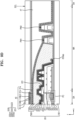
- FIG. 10 is a cross-sectional view schematically illustrating a display panel according to some embodiments, which may correspond to a cross-section taken along the line V-V' of FIG. 5 .
- the edges 222ae and 222ce of the first and second functional layers 222a and 222c and the edge 223e of the opposite electrode 223 may be located on the second organic insulating layer 211.
- the edge 320e of the organic encapsulation layer 320 may be located on one side of the first partition PW1 (e.g., the other side of the first partition PW1 facing the second partition PW2) as in the embodiments described above.
- the edge 320e of the organic encapsulation layer 320 illustrated in FIG. 11B may be located on the upper surface of the first partition PW1 unlike the illustration of FIG. 11A .
- the organic residues 320r may be arranged spaced apart from each other.
- One organic residue 320r may be arranged adjacent to the first partition PW1, the other organic residue 320r may be arranged adjacent to the second partition PW2, and the organic residues 320r may be spaced apart from each other.
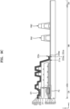
- the display panel 10 includes two partitions; however, as illustrated in FIG. 11C , the display panel 10 may include three or more partitions.
- the third partition PW3 may be arranged closer to the opening area, that is, the opening 10H of the display panel 10 (see FIG. 6 ), than the first partition PW1 and the second partition PW2.
- the first to third partitions PW1, PW2, and PW3 may have different heights.
- a height H2 of the second partition PW2 may be greater than a height H1 of the first partition PW1 and a height H3 of the third partition PW3, and the height H1 of the first partition PW1 may be greater than the height H3 of the third partition PW3.
- a plurality of partitions may be used to monitor the position of the organic encapsulation layer 320.
Landscapes
- Physics & Mathematics (AREA)
- Optics & Photonics (AREA)
- Chemical & Material Sciences (AREA)
- Inorganic Chemistry (AREA)
- Engineering & Computer Science (AREA)
- Microelectronics & Electronic Packaging (AREA)
- Life Sciences & Earth Sciences (AREA)
- Sustainable Development (AREA)
- Electroluminescent Light Sources (AREA)
- Devices For Indicating Variable Information By Combining Individual Elements (AREA)
Claims (13)
- Anzeigetafel (10), Folgendes umfassend:ein Substrat (100), das eine Öffnung (10H) einschließt, die von einer Oberseite zu einer Unterseite des Substrats (100) durchdringt;eine Leuchtdiode (OLED) in einem Anzeigebereich (DA) rings um die Öffnung (10H) und Folgendes einschließend:eine Pixelelektrode (221);eine Gegenelektrode (223);eine Zwischenschicht (222) zwischen der Pixelelektrode (221) und der Gegenelektrode (223), wobei die Zwischenschicht (222) eine Emissionsschicht (222b) und mindestens eine Schicht aus organischem Material (222a, 222c) umfasst;eine Dünnschicht-Verkapselungsschicht (300) auf der Leuchtdiode (OLED), und die eine organische Verkapselungsschicht (320) und mindestens eine anorganische Verkapselungsschicht (310, 330) einschließt; undeinen Transistor (TFT), der mit der Leuchtdiode (OLED) elektrisch verbunden ist; undeine organische Isolierschicht (211) zwischen dem Transistor (TFT) und der Leuchtdiode (OLED),wobei sich die Gegenelektrode (223) und mindestens eine Schicht aus organischem Material (222a, 222c) der Zwischenschicht (222) in Richtung der Öffnung (10H) erstrecken, wobei ein Randabschnitt der Gegenelektrode (223), welcher der Öffnung (10H) zugewandt ist, weiter in Richtung der Öffnung (10H) vorspringt als die mindestens eine Schicht aus organischem Material (222a, 222c) und einen Grat einschließt, der mit der organischen Verkapselungsschicht (320) bedeckt ist, undwobei sich die mindestens eine Schicht aus organischem Material (222a, 222c) und die Gegenelektrode (223) jeweils über einen Rand (211e) der organischen Isolierschicht (211) hinaus in Richtung der Öffnung (10H) erstrecken.
- Anzeigetafel nach Anspruch 1, wobei die mindestens eine Schicht aus organischem Material mindestens eine von einer Löchertransportschicht, einer Löcherinjektionsschicht, einer Elektronentransportschicht oder einer Elektroneninjektionsschicht einschließt.
- Anzeigetafel (10) nach einem der Ansprüche 1 bis 2, wobei der Grat Silber (Ag), Magnesium (Mg), Aluminium (Al), Platin (Pt), Palladium (Pd), Gold (Au), Nickel (Ni), Neodym (Nd), Iridium (Ir), Chrom (Cr), Lithium (Li), Kalzium (Ca) oder eine Legierung davon einschließt.
- Anzeigetafel (10) nach einem der Ansprüche 1 bis 3, ferner eine erste Trennwand (PW1) zwischen dem Anzeigebereich (DA) und der Öffnung (10H) umfassend,
wobei ein Rand (223e) der Gegenelektrode (223) und ein Rand (222ae, 222ce) der mindestens einen Schicht aus organischem Material (222a, 222c) näher an dem Anzeigebereich (DA) liegt als die erste Trennwand (PW1). - Anzeigetafel (10) nach Anspruch 4, ferner eine zweite Trennwand (PW2) umfassend, die näher an der Öffnung (10H) liegt als die erste Trennwand (PW1),
wobei sich eine Höhe (H2) der zweiten Trennwand (PW2) von einer Höhe (H1) der ersten Trennwand (PW1) unterscheidet, optional wobei:das Anzeigetafel (10) ferner eine dritte Trennwand (PW3) umfasst, die näher an der Öffnung (10H) liegt als die zweite Trennwand (PW2),wobei eine Höhe (H3) der dritten Trennwand (PW3) kleiner ist als die Höhe (H1) der ersten Trennwand (PW1) und die Höhe (H2) der zweiten Trennwand (PW2). - Anzeigetafel (10) nach einem der Ansprüche 3 bis 5, ferner eine Struktur auf der organischen Isolierschicht (211) umfassend und eine Vielzahl von Vorsprüngen (PS) und eine konkave Mulde (VY) zwischen der Vielzahl von Vorsprüngen (PS) einschließend,
wobei sich ein Abschnitt der organischen Verkapselungsschicht (320) in der konkaven Mulde (VY) befindet, optional wobei:die Anzeigetafel (10) ferner Signalleitungen (DL, SL) auf dem Substrat (100) umfasst,wobei mindestens eine der Signalleitungen einen Umgehungsabschnitt (DL-C) einschließt, der die Öffnung (10H) umgeht, wobei der Umgehungsabschnitt (DL-C) die Vielzahl von Vorsprüngen (PS) oder die konkave Mulde (VY) überlappt. - Anzeigetafel (10) nach einem der Ansprüche 3 bis 6, wobei die mindestens eine anorganische Verkapselungsschicht (310, 330) eine erste anorganische Verkapselungsschicht (310) unter der organischen Verkapselungsschicht (320) und eine zweite anorganische Verkapselungsschicht (330) auf der organischen Verkapselungsschicht (320) einschließt, wobei die erste anorganische Verkapselungsschicht (310) und die zweite anorganische Verkapselungsschicht (330) einander in einem Bereich zwischen der ersten Trennwand (PW1) und der Öffnung (10H) direkt berühren.
- Anzeigetafel (10) nach Anspruch 7, ferner eine Planarisierungsisolierschicht (47) auf der zweiten anorganischen Verkapselungsschicht (330) umfassend, und die einen Abschnitt der organischen Verkapselungsschicht (320) und die erste Trennwand (PW1) überlappt und ein organisches Isoliermaterial einschließt.
- Anzeigetafel (10) nach Anspruch 8, wobei:(i) die Planarisierungsisolierschicht (47) eine Form einer geschlossenen Schleife aufweist, die einen Umfang der Öffnung (10H) bedeckt; und/oder(ii) die Planarisierungsisolierschicht (47) den Anzeigebereich (DA) und einen Umfang der Öffnung (10H) bedeckt.
- Elektronische Vorrichtung (1), umfassend eine Anzeigetafel (10) nach einem der Ansprüche 1 bis 9, und wobei die elektronische Vorrichtung (1) ferner umfasst:einen Zwischenbereich (MA) zwischen der Öffnung (10H) und dem Anzeigebereich (DA); undeine Komponente (70), welche die Öffnung (10H) überlappt.
- Elektronische Vorrichtung (1) nach Anspruch 10, wobei die Anzeigetafel (10) ferner eine Eingabeerfassungsschicht (40) auf der Dünnschicht-Verkapselungsschicht (300) umfasst und mindestens eine leitfähige Schicht (CML1, CML2) und mindestens eine Isolierschicht (41a, 41b, 43, 45) einschließt.
- Elektronische Vorrichtung nach Anspruch 11, wobei:
die mindestens eine Isolierschicht (41a, 41b, 43, 45) der Eingabeerfassungsschicht (40) die Planarisierungsisolierschicht (47) einschließt und einen Umfang der Öffnung (10H) und den Anzeigebereich (DA) bedeckt. - Elektronische Vorrichtung (1) nach einem der Ansprüche 11 bis 12, wobei:
die Komponente (70) einen Sensor oder eine Kamera umfasst.
Applications Claiming Priority (1)
| Application Number | Priority Date | Filing Date | Title |
|---|---|---|---|
| KR1020200093033A KR102870802B1 (ko) | 2020-07-27 | 2020-07-27 | 표시 패널 및 이를 포함하는 전자 기기 |
Publications (2)
| Publication Number | Publication Date |
|---|---|
| EP3945592A1 EP3945592A1 (de) | 2022-02-02 |
| EP3945592B1 true EP3945592B1 (de) | 2025-04-09 |
Family
ID=77042724
Family Applications (1)
| Application Number | Title | Priority Date | Filing Date |
|---|---|---|---|
| EP21187244.5A Active EP3945592B1 (de) | 2020-07-27 | 2021-07-22 | Anzeigetafel und elektronische vorrichtung damit |
Country Status (4)
| Country | Link |
|---|---|
| US (1) | US11925052B2 (de) |
| EP (1) | EP3945592B1 (de) |
| KR (1) | KR102870802B1 (de) |
| CN (1) | CN113990897A (de) |
Families Citing this family (5)
| Publication number | Priority date | Publication date | Assignee | Title |
|---|---|---|---|---|
| KR102792881B1 (ko) | 2020-11-12 | 2025-04-08 | 삼성디스플레이 주식회사 | 표시 장치 |
| KR20220086917A (ko) * | 2020-12-17 | 2022-06-24 | 엘지디스플레이 주식회사 | 발광 표시 장치와 이를 이용한 멀티 스크린 표시 장치 |
| KR20230082281A (ko) * | 2021-12-01 | 2023-06-08 | 엘지디스플레이 주식회사 | 발광 표시 장치 |
| KR20240008460A (ko) * | 2022-07-11 | 2024-01-19 | 삼성디스플레이 주식회사 | 표시 장치 및 표시 장치의 제조 방법. |
| CN121038522A (zh) * | 2024-05-28 | 2025-11-28 | 京东方科技集团股份有限公司 | 显示基板及其制备方法和显示装置 |
Citations (1)
| Publication number | Priority date | Publication date | Assignee | Title |
|---|---|---|---|---|
| US20170288004A1 (en) * | 2016-04-05 | 2017-10-05 | Samsung Display Co., Ltd. | Display device |
Family Cites Families (16)
| Publication number | Priority date | Publication date | Assignee | Title |
|---|---|---|---|---|
| KR101483193B1 (ko) | 2008-04-22 | 2015-01-16 | 주성엔지니어링(주) | 박막 패터닝 방법 및 이를 이용한 전기 광학 소자 |
| KR102407869B1 (ko) | 2016-02-16 | 2022-06-13 | 삼성디스플레이 주식회사 | 유기 발광 디스플레이 장치와, 이의 제조 방법 |
| KR102641816B1 (ko) | 2016-07-19 | 2024-02-29 | 삼성디스플레이 주식회사 | 디스플레이 장치 |
| CN111567142B (zh) | 2017-12-27 | 2023-06-13 | 夏普株式会社 | 显示装置及其制造方法 |
| KR102552266B1 (ko) * | 2018-01-31 | 2023-07-07 | 삼성디스플레이 주식회사 | 표시 장치 |
| KR102632613B1 (ko) | 2018-09-19 | 2024-02-02 | 삼성디스플레이 주식회사 | 표시 패널 |
| US10541380B1 (en) | 2018-08-30 | 2020-01-21 | Samsung Display Co., Ltd. | Display device with substrate comprising an opening and adjacent grooves |
| KR102612036B1 (ko) | 2018-09-27 | 2023-12-11 | 삼성디스플레이 주식회사 | 표시 패널 및 이를 포함한 전자 장치 |
| KR102663899B1 (ko) * | 2018-09-28 | 2024-05-09 | 삼성디스플레이 주식회사 | 표시 패널 |
| KR20200049115A (ko) | 2018-10-31 | 2020-05-08 | 엘지디스플레이 주식회사 | 투명 유기 발광 표시 장치 및 이의 제조방법 |
| KR102659189B1 (ko) | 2018-11-27 | 2024-04-19 | 삼성디스플레이 주식회사 | 표시장치 |
| KR102682395B1 (ko) * | 2018-12-26 | 2024-07-09 | 삼성디스플레이 주식회사 | 유기발광 표시장치 및 유기발광 표시장치의 제조방법 |
| KR102730281B1 (ko) | 2018-12-28 | 2024-11-13 | 엘지디스플레이 주식회사 | 관통홀이 구비된 표시장치 |
| US20200357869A1 (en) * | 2019-05-10 | 2020-11-12 | Samsung Display Co., Ltd. | Display apparatus and method of manufacturing the same |
| KR102712664B1 (ko) | 2019-06-18 | 2024-10-04 | 삼성디스플레이 주식회사 | 디스플레이 장치 및 이의 제조 방법 |
| KR102822186B1 (ko) | 2019-10-14 | 2025-06-19 | 삼성디스플레이 주식회사 | 표시 장치 및 그 제조방법 |
-
2020
- 2020-07-27 KR KR1020200093033A patent/KR102870802B1/ko active Active
-
2021
- 2021-06-02 US US17/337,304 patent/US11925052B2/en active Active
- 2021-07-22 EP EP21187244.5A patent/EP3945592B1/de active Active
- 2021-07-27 CN CN202110849465.4A patent/CN113990897A/zh active Pending
Patent Citations (1)
| Publication number | Priority date | Publication date | Assignee | Title |
|---|---|---|---|---|
| US20170288004A1 (en) * | 2016-04-05 | 2017-10-05 | Samsung Display Co., Ltd. | Display device |
Also Published As
| Publication number | Publication date |
|---|---|
| EP3945592A1 (de) | 2022-02-02 |
| KR102870802B1 (ko) | 2025-10-14 |
| US11925052B2 (en) | 2024-03-05 |
| CN113990897A (zh) | 2022-01-28 |
| KR20220014425A (ko) | 2022-02-07 |
| US20220029130A1 (en) | 2022-01-27 |
Similar Documents
| Publication | Publication Date | Title |
|---|---|---|
| US11925052B2 (en) | Display panel and electronic apparatus including the same | |
| EP3863060B1 (de) | Anzeigevorrichtung | |
| KR102902403B1 (ko) | 표시 패널, 그 제조 방법 및 전자 기기 | |
| CN113439349B (zh) | 显示面板 | |
| KR102959765B1 (ko) | 표시 패널 및 전자 기기 | |
| KR20200113092A (ko) | 표시 패널 | |
| KR20200107026A (ko) | 표시 패널 | |
| US11683949B2 (en) | Flexible cover window and foldable display apparatus | |
| KR20210131507A (ko) | 디스플레이 장치 및 그 제조방법 | |
| CN114649389A (zh) | 显示面板 | |
| KR20220004856A (ko) | 디스플레이 패널과, 이의 제조방법 | |
| KR20210044359A (ko) | 표시 장치 및 그 제조방법 | |
| US12069894B2 (en) | Display apparatus comprising irradiated regions and dams and method of manufacturing the same | |
| KR102952961B1 (ko) | 표시 장치 | |
| CN117915700A (zh) | 显示面板及包括显示面板的电子装置 | |
| CN222126533U (zh) | 显示面板及包括其的电子设备 | |
| CN218831215U (zh) | 显示装置 | |
| KR102203105B1 (ko) | 디스플레이 장치 | |
| US20250261522A1 (en) | Display panel | |
| US20260068402A1 (en) | Display apparatus, electronic device including the same, and methods of manufacturing display apparatus | |
| KR20250063960A (ko) | 표시장치 및 표시장치의 제조방법 | |
| KR20260062922A (ko) | 표시 패널 | |
| KR20240165825A (ko) | 표시 패널 및 이를 포함하는 전자 기기 | |
| CN118076161A (zh) | 显示装置 |
Legal Events
| Date | Code | Title | Description |
|---|---|---|---|
| PUAI | Public reference made under article 153(3) epc to a published international application that has entered the european phase |
Free format text: ORIGINAL CODE: 0009012 |
|
| STAA | Information on the status of an ep patent application or granted ep patent |
Free format text: STATUS: THE APPLICATION HAS BEEN PUBLISHED |
|
| AK | Designated contracting states |
Kind code of ref document: A1 Designated state(s): AL AT BE BG CH CY CZ DE DK EE ES FI FR GB GR HR HU IE IS IT LI LT LU LV MC MK MT NL NO PL PT RO RS SE SI SK SM TR |
|
| STAA | Information on the status of an ep patent application or granted ep patent |
Free format text: STATUS: REQUEST FOR EXAMINATION WAS MADE |
|
| 17P | Request for examination filed |
Effective date: 20220329 |
|
| RBV | Designated contracting states (corrected) |
Designated state(s): AL AT BE BG CH CY CZ DE DK EE ES FI FR GB GR HR HU IE IS IT LI LT LU LV MC MK MT NL NO PL PT RO RS SE SI SK SM TR |
|
| P01 | Opt-out of the competence of the unified patent court (upc) registered |
Effective date: 20230516 |
|
| REG | Reference to a national code |
Ref country code: DE Ref legal event code: R079 Free format text: PREVIOUS MAIN CLASS: H01L0027320000 Ipc: H10K0050160000 Ref document number: 602021028798 Country of ref document: DE |
|
| GRAP | Despatch of communication of intention to grant a patent |
Free format text: ORIGINAL CODE: EPIDOSNIGR1 |
|
| STAA | Information on the status of an ep patent application or granted ep patent |
Free format text: STATUS: GRANT OF PATENT IS INTENDED |
|
| RIC1 | Information provided on ipc code assigned before grant |
Ipc: H10K 59/65 20230101ALN20241010BHEP Ipc: H10K 50/15 20230101ALI20241010BHEP Ipc: H10K 59/80 20230101ALI20241010BHEP Ipc: H10K 59/124 20230101ALI20241010BHEP Ipc: H10K 50/16 20230101AFI20241010BHEP |
|
| RIC1 | Information provided on ipc code assigned before grant |
Ipc: H10K 59/65 20230101ALN20241016BHEP Ipc: H10K 50/15 20230101ALI20241016BHEP Ipc: H10K 59/80 20230101ALI20241016BHEP Ipc: H10K 59/124 20230101ALI20241016BHEP Ipc: H10K 50/16 20230101AFI20241016BHEP |
|
| INTG | Intention to grant announced |
Effective date: 20241030 |
|
| RIN1 | Information on inventor provided before grant (corrected) |
Inventor name: LEE, JIHWANG Inventor name: KIM, SANGYEOL Inventor name: KIM, JAEHYUN Inventor name: CHOI, YOUNGSEO Inventor name: SEO, SEUNGWOO |
|
| GRAS | Grant fee paid |
Free format text: ORIGINAL CODE: EPIDOSNIGR3 |
|
| GRAA | (expected) grant |
Free format text: ORIGINAL CODE: 0009210 |
|
| STAA | Information on the status of an ep patent application or granted ep patent |
Free format text: STATUS: THE PATENT HAS BEEN GRANTED |
|
| AK | Designated contracting states |
Kind code of ref document: B1 Designated state(s): AL AT BE BG CH CY CZ DE DK EE ES FI FR GB GR HR HU IE IS IT LI LT LU LV MC MK MT NL NO PL PT RO RS SE SI SK SM TR |
|
| REG | Reference to a national code |
Ref country code: GB Ref legal event code: FG4D |
|
| REG | Reference to a national code |
Ref country code: CH Ref legal event code: EP |
|
| REG | Reference to a national code |
Ref country code: DE Ref legal event code: R096 Ref document number: 602021028798 Country of ref document: DE |
|
| REG | Reference to a national code |
Ref country code: IE Ref legal event code: FG4D |
|
| PGFP | Annual fee paid to national office [announced via postgrant information from national office to epo] |
Ref country code: GB Payment date: 20250624 Year of fee payment: 5 |
|
| PGFP | Annual fee paid to national office [announced via postgrant information from national office to epo] |
Ref country code: FR Payment date: 20250624 Year of fee payment: 5 |
|
| REG | Reference to a national code |
Ref country code: NL Ref legal event code: MP Effective date: 20250409 |
|
| PG25 | Lapsed in a contracting state [announced via postgrant information from national office to epo] |
Ref country code: NL Free format text: LAPSE BECAUSE OF FAILURE TO SUBMIT A TRANSLATION OF THE DESCRIPTION OR TO PAY THE FEE WITHIN THE PRESCRIBED TIME-LIMIT Effective date: 20250409 |
|
| REG | Reference to a national code |
Ref country code: AT Ref legal event code: MK05 Ref document number: 1784815 Country of ref document: AT Kind code of ref document: T Effective date: 20250409 |
|
| PG25 | Lapsed in a contracting state [announced via postgrant information from national office to epo] |
Ref country code: FI Free format text: LAPSE BECAUSE OF FAILURE TO SUBMIT A TRANSLATION OF THE DESCRIPTION OR TO PAY THE FEE WITHIN THE PRESCRIBED TIME-LIMIT Effective date: 20250409 Ref country code: ES Free format text: LAPSE BECAUSE OF FAILURE TO SUBMIT A TRANSLATION OF THE DESCRIPTION OR TO PAY THE FEE WITHIN THE PRESCRIBED TIME-LIMIT Effective date: 20250409 Ref country code: PT Free format text: LAPSE BECAUSE OF FAILURE TO SUBMIT A TRANSLATION OF THE DESCRIPTION OR TO PAY THE FEE WITHIN THE PRESCRIBED TIME-LIMIT Effective date: 20250811 |
|
| PGFP | Annual fee paid to national office [announced via postgrant information from national office to epo] |
Ref country code: DE Payment date: 20250624 Year of fee payment: 5 |
|
| REG | Reference to a national code |
Ref country code: LT Ref legal event code: MG9D |
|
| PG25 | Lapsed in a contracting state [announced via postgrant information from national office to epo] |
Ref country code: NO Free format text: LAPSE BECAUSE OF FAILURE TO SUBMIT A TRANSLATION OF THE DESCRIPTION OR TO PAY THE FEE WITHIN THE PRESCRIBED TIME-LIMIT Effective date: 20250709 Ref country code: GR Free format text: LAPSE BECAUSE OF FAILURE TO SUBMIT A TRANSLATION OF THE DESCRIPTION OR TO PAY THE FEE WITHIN THE PRESCRIBED TIME-LIMIT Effective date: 20250710 |
|
| PG25 | Lapsed in a contracting state [announced via postgrant information from national office to epo] |
Ref country code: PL Free format text: LAPSE BECAUSE OF FAILURE TO SUBMIT A TRANSLATION OF THE DESCRIPTION OR TO PAY THE FEE WITHIN THE PRESCRIBED TIME-LIMIT Effective date: 20250409 |
|
| PG25 | Lapsed in a contracting state [announced via postgrant information from national office to epo] |
Ref country code: BG Free format text: LAPSE BECAUSE OF FAILURE TO SUBMIT A TRANSLATION OF THE DESCRIPTION OR TO PAY THE FEE WITHIN THE PRESCRIBED TIME-LIMIT Effective date: 20250409 |
|
| PG25 | Lapsed in a contracting state [announced via postgrant information from national office to epo] |
Ref country code: HR Free format text: LAPSE BECAUSE OF FAILURE TO SUBMIT A TRANSLATION OF THE DESCRIPTION OR TO PAY THE FEE WITHIN THE PRESCRIBED TIME-LIMIT Effective date: 20250409 |
|
| PG25 | Lapsed in a contracting state [announced via postgrant information from national office to epo] |
Ref country code: AT Free format text: LAPSE BECAUSE OF FAILURE TO SUBMIT A TRANSLATION OF THE DESCRIPTION OR TO PAY THE FEE WITHIN THE PRESCRIBED TIME-LIMIT Effective date: 20250409 |
|
| PG25 | Lapsed in a contracting state [announced via postgrant information from national office to epo] |
Ref country code: RS Free format text: LAPSE BECAUSE OF FAILURE TO SUBMIT A TRANSLATION OF THE DESCRIPTION OR TO PAY THE FEE WITHIN THE PRESCRIBED TIME-LIMIT Effective date: 20250709 |
|
| PG25 | Lapsed in a contracting state [announced via postgrant information from national office to epo] |
Ref country code: IS Free format text: LAPSE BECAUSE OF FAILURE TO SUBMIT A TRANSLATION OF THE DESCRIPTION OR TO PAY THE FEE WITHIN THE PRESCRIBED TIME-LIMIT Effective date: 20250809 |
|
| PG25 | Lapsed in a contracting state [announced via postgrant information from national office to epo] |
Ref country code: LV Free format text: LAPSE BECAUSE OF FAILURE TO SUBMIT A TRANSLATION OF THE DESCRIPTION OR TO PAY THE FEE WITHIN THE PRESCRIBED TIME-LIMIT Effective date: 20250409 |
|
| REG | Reference to a national code |
Ref country code: DE Ref legal event code: R097 Ref document number: 602021028798 Country of ref document: DE |
|
| PG25 | Lapsed in a contracting state [announced via postgrant information from national office to epo] |
Ref country code: DK Free format text: LAPSE BECAUSE OF FAILURE TO SUBMIT A TRANSLATION OF THE DESCRIPTION OR TO PAY THE FEE WITHIN THE PRESCRIBED TIME-LIMIT Effective date: 20250409 Ref country code: SM Free format text: LAPSE BECAUSE OF FAILURE TO SUBMIT A TRANSLATION OF THE DESCRIPTION OR TO PAY THE FEE WITHIN THE PRESCRIBED TIME-LIMIT Effective date: 20250409 |
|
| PG25 | Lapsed in a contracting state [announced via postgrant information from national office to epo] |
Ref country code: CZ Free format text: LAPSE BECAUSE OF FAILURE TO SUBMIT A TRANSLATION OF THE DESCRIPTION OR TO PAY THE FEE WITHIN THE PRESCRIBED TIME-LIMIT Effective date: 20250409 |
|
| PG25 | Lapsed in a contracting state [announced via postgrant information from national office to epo] |
Ref country code: EE Free format text: LAPSE BECAUSE OF FAILURE TO SUBMIT A TRANSLATION OF THE DESCRIPTION OR TO PAY THE FEE WITHIN THE PRESCRIBED TIME-LIMIT Effective date: 20250409 |
|
| PG25 | Lapsed in a contracting state [announced via postgrant information from national office to epo] |
Ref country code: RO Free format text: LAPSE BECAUSE OF FAILURE TO SUBMIT A TRANSLATION OF THE DESCRIPTION OR TO PAY THE FEE WITHIN THE PRESCRIBED TIME-LIMIT Effective date: 20250409 Ref country code: SK Free format text: LAPSE BECAUSE OF FAILURE TO SUBMIT A TRANSLATION OF THE DESCRIPTION OR TO PAY THE FEE WITHIN THE PRESCRIBED TIME-LIMIT Effective date: 20250409 |
|
| PG25 | Lapsed in a contracting state [announced via postgrant information from national office to epo] |
Ref country code: IT Free format text: LAPSE BECAUSE OF FAILURE TO SUBMIT A TRANSLATION OF THE DESCRIPTION OR TO PAY THE FEE WITHIN THE PRESCRIBED TIME-LIMIT Effective date: 20250409 |
|
| PLBE | No opposition filed within time limit |
Free format text: ORIGINAL CODE: 0009261 |
|
| STAA | Information on the status of an ep patent application or granted ep patent |
Free format text: STATUS: NO OPPOSITION FILED WITHIN TIME LIMIT |
|
| REG | Reference to a national code |
Ref country code: CH Ref legal event code: L10 Free format text: ST27 STATUS EVENT CODE: U-0-0-L10-L00 (AS PROVIDED BY THE NATIONAL OFFICE) Effective date: 20260218 |
|
| REG | Reference to a national code |
Ref country code: CH Ref legal event code: H13 Free format text: ST27 STATUS EVENT CODE: U-0-0-H10-H13 (AS PROVIDED BY THE NATIONAL OFFICE) Effective date: 20260224 |
|
| PG25 | Lapsed in a contracting state [announced via postgrant information from national office to epo] |
Ref country code: LU Free format text: LAPSE BECAUSE OF NON-PAYMENT OF DUE FEES Effective date: 20250722 |
|
| 26N | No opposition filed |
Effective date: 20260112 |
|
| REG | Reference to a national code |
Ref country code: BE Ref legal event code: MM Effective date: 20250731 |
|
| PG25 | Lapsed in a contracting state [announced via postgrant information from national office to epo] |
Ref country code: BE Free format text: LAPSE BECAUSE OF NON-PAYMENT OF DUE FEES Effective date: 20250731 |
|
| PG25 | Lapsed in a contracting state [announced via postgrant information from national office to epo] |
Ref country code: CH Free format text: LAPSE BECAUSE OF NON-PAYMENT OF DUE FEES Effective date: 20250731 |