EP3944477B1 - Wechselrichter und elektromotor mit einem solchen wechselrichter - Google Patents
Wechselrichter und elektromotor mit einem solchen wechselrichter Download PDFInfo
- Publication number
- EP3944477B1 EP3944477B1 EP20187148.0A EP20187148A EP3944477B1 EP 3944477 B1 EP3944477 B1 EP 3944477B1 EP 20187148 A EP20187148 A EP 20187148A EP 3944477 B1 EP3944477 B1 EP 3944477B1
- Authority
- EP
- European Patent Office
- Prior art keywords
- inverter
- board
- capacitor board
- transistor
- carrier
- Prior art date
- Legal status (The legal status is an assumption and is not a legal conclusion. Google has not performed a legal analysis and makes no representation as to the accuracy of the status listed.)
- Active
Links
Images


Classifications
-
- H—ELECTRICITY
- H02—GENERATION; CONVERSION OR DISTRIBUTION OF ELECTRIC POWER
- H02K—DYNAMO-ELECTRIC MACHINES
- H02K11/00—Structural association of dynamo-electric machines with electric components or with devices for shielding, monitoring or protection
- H02K11/30—Structural association with control circuits or drive circuits
- H02K11/33—Drive circuits, e.g. power electronics
-
- H—ELECTRICITY
- H02—GENERATION; CONVERSION OR DISTRIBUTION OF ELECTRIC POWER
- H02K—DYNAMO-ELECTRIC MACHINES
- H02K11/00—Structural association of dynamo-electric machines with electric components or with devices for shielding, monitoring or protection
- H02K11/04—Structural association of dynamo-electric machines with electric components or with devices for shielding, monitoring or protection for rectification
- H02K11/049—Rectifiers associated with stationary parts, e.g. stator cores
- H02K11/05—Rectifiers associated with casings, enclosures or brackets
-
- H—ELECTRICITY
- H02—GENERATION; CONVERSION OR DISTRIBUTION OF ELECTRIC POWER
- H02K—DYNAMO-ELECTRIC MACHINES
- H02K5/00—Casings; Enclosures; Supports
- H02K5/04—Casings or enclosures characterised by the shape, form or construction thereof
- H02K5/22—Auxiliary parts of casings not covered by groups H02K5/06-H02K5/20, e.g. shaped to form connection boxes or terminal boxes
- H02K5/225—Terminal boxes or connection arrangements
-
- H—ELECTRICITY
- H02—GENERATION; CONVERSION OR DISTRIBUTION OF ELECTRIC POWER
- H02K—DYNAMO-ELECTRIC MACHINES
- H02K9/00—Arrangements for cooling or ventilating
- H02K9/19—Arrangements for cooling or ventilating for machines with closed casing and closed-circuit cooling using a liquid cooling medium, e.g. oil
- H02K9/197—Arrangements for cooling or ventilating for machines with closed casing and closed-circuit cooling using a liquid cooling medium, e.g. oil in which the rotor or stator space is fluid-tight, e.g. to provide for different cooling media for rotor and stator
-
- H—ELECTRICITY
- H02—GENERATION; CONVERSION OR DISTRIBUTION OF ELECTRIC POWER
- H02K—DYNAMO-ELECTRIC MACHINES
- H02K2203/00—Specific aspects not provided for in the other groups of this subclass relating to the windings
- H02K2203/03—Machines characterised by the wiring boards, i.e. printed circuit boards or similar structures for connecting the winding terminations
-
- H—ELECTRICITY
- H02—GENERATION; CONVERSION OR DISTRIBUTION OF ELECTRIC POWER
- H02K—DYNAMO-ELECTRIC MACHINES
- H02K2203/00—Specific aspects not provided for in the other groups of this subclass relating to the windings
- H02K2203/09—Machines characterised by wiring elements other than wires, e.g. bus rings, for connecting the winding terminations
-
- H—ELECTRICITY
- H02—GENERATION; CONVERSION OR DISTRIBUTION OF ELECTRIC POWER
- H02K—DYNAMO-ELECTRIC MACHINES
- H02K2213/00—Specific aspects, not otherwise provided for and not covered by codes H02K2201/00 - H02K2211/00
- H02K2213/12—Machines characterised by the modularity of some components
-
- H—ELECTRICITY
- H02—GENERATION; CONVERSION OR DISTRIBUTION OF ELECTRIC POWER
- H02K—DYNAMO-ELECTRIC MACHINES
- H02K5/00—Casings; Enclosures; Supports
- H02K5/04—Casings or enclosures characterised by the shape, form or construction thereof
- H02K5/20—Casings or enclosures characterised by the shape, form or construction thereof with channels or ducts for flow of cooling medium
Definitions
- the invention relates to an inverter for an electric motor according to the preamble of Claim 1.
- the invention also relates to an electric motor having the inverter.
- An electric motor having an inverter is known for example from US 2016/065030 A1 , US 2008/284272 A1 and JP 2016146702 A .
- the electric motor comprises a rotor and a stator which electromagnetically interact with one another.
- the inverter comprises a capacitor board with capacitors, a transistor board with transistors and a control circuit board and converts the direct current into the three-phase current for the stator.
- the same In order to feed the direct current into the inverter, the same usually comprises battery terminals assigned to the positive pole and the negative pole.
- the design of the battery terminals is often highly complex as a result of which the manufacturing costs and the assembly expenditure are increased.
- the object of the invention therefore is to state an improved or at least alternative embodiment for an inverter of the generic type, with which the described disadvantages are overcome.
- the object of the invention also is to provide an electric motor having such an inverter.
- the inverter comprises a capacitor board having multiple capacitors, multiple transistor boards each with multiple transistors and a control circuit board.
- the capacitor board, the respective transistor boards and the control circuit board lie axially on top of one another and are electrically interconnected with one another.
- the inverter comprises a battery terminal each which are connected to the capacitor board in an electrically conductive manner and axially project from the capacitor board.
- the battery terminals can be screwed to the capacitor board.
- the battery terminals are identical to one another and are each formed by a connector having an external dielectric casing and internal electrically conductive lines.
- the battery terminals according to the invention are advantageously of a simple design and because of this the manufacturing expenditure and the assembly expenditure of the battery terminals in the inverter reduced.
- axial and radial in connection with the present invention relate to a longitudinal centre axis of the inverter.
- the capacitor board, the control circuit board and the transistor boards orientated in the inverter perpendicularly to the longitudinal centre axis.
- the transistors are primarily MOSFET.
- the capacitors are arranged annularly on the capacitor board.
- the battery terminals are then arranged between the capacitors and centrally on the capacitor board.
- the respective battery terminal comprises three pole contact for contacting to the capacitor board, wherein the pole contacts of the one battery terminal and the pole contacts of the other battery terminal are arranged in a circle on the capacitor board and alternately arranging one another in the circle.
- the pole contacts of the battery terminals can be arranged symmetrically in the centre of the capacitor board. Through the symmetry created on the capacitor board, negative effects and losses in the inverter can be minimised.
- the respective battery terminal can comprise a bridge that is parallel to the capacitor board, which connects the central pole contact with a lateral pole contact in an electrically conductive manner.
- the respective battery terminal can additionally comprise a second bridge that is parallel to the capacitor board, which connects the central pole contact with the other lateral pole contact in an electrically conductive manner.
- the first bridge and the second bridge are axially offset to one another and orientated at an angle to one another.
- the first bridge of the one battery terminal in each case can bridge the second bridge of the other battery terminal, so that the pole contacts of the one battery terminal and the pole contacts of the other battery terminal are arranged in a circle and alternating one another in the circle. Because of this, the pole contacts of the negative pole and the pole contacts of the positive pole are also arranged alternately and in a circle.
- a contact connector is formed, which axially projects from the capacitor board and leads to the outside.
- the pole contacts of the respective battery terminal are contactable towards the outside in an electrically conductive manner.
- the inverter comprises a hollow-cylindrical carrier with a centre axis.
- the carrier carries the capacitor board, the transistor boards and the control circuit board and encases these in the circumferential direction towards the outside.
- an annular rear ring that is orientated transversely to the centre axis is additionally integrally formed.
- the carrier ring is formed annularly, so that an opening located in the centre is formed in the carrier ring.
- the battery terminals project through the opening of the annular carrier ring to the outside.
- the term "carry” in the context with the present invention means that the capacitor board, the transistor boards and the control circuit board are aligned in the right position to each other via the carrier.
- a pressure plate is firmly connected to a cooling plate, so that an elastically deformable foam pad, the capacitor board, the carrier ring, and the transistor boards are pressed together i.e. are sandwiched between the pressure plate and the cooling plate.
- the inverter forms a contiguous assembly unit with the carrier, the capacitor board, the transistor boards, the cooling plate and the control circuit board ready for assembly.
- the inverter can be finish-assembled independently of further elements of the electric motor. Because of this, both the effort and also the costs can be reduced.
- the inverter can be tested for its functionality even prior to the assembly on further elements of the electric motor.
- the carrier is preferentially formed from plastic and not electrically conductive.
- the carrier protects the capacitor board, the transistor boards and the control circuit board towards the outside and aligns the same relative to one another.
- the capacitor board, the transistor boards and the control circuit board are arranged in the carrier sandwich-like on top of one another and axially spaced apart from one another, wherein the capacitor board is preferentially arranged between the control circuit board and the transistor boards.
- the centre axis of the carrier coincides with the longitudinal centre axis of the inverter, so that accordingly the capacitor board, the transistor boards and the control circuit board are arranged perpendicularly to the centre axis.
- the transistor boards are fastened on the annular carrier ring, facing away from the capacitor board and circulating about the centre axis in a distributed and clamping manner.
- the carrier ring divides an interior space of the carrier into two axially adjacent regions, wherein in the first region the transistor boards and in the second axial region the capacitor board and the control circuit board are received and fixed. In other words, the capacitor board and the transistor boards are separated from one another and electrically insulated by the carrier ring.
- multiple slots can be formed in the carrier ring in which a contact bus bar each is received.
- the respective contact bus bar is then compressed between the respective transistor board and the capacitor board and because of this the transistor boards are electrically contacted with the capacitor board.
- the respective contact bus bar is securely fixed between the capacitor board and the respective transistor board.
- the foam pad By way of the foam pad, an adequately high pressure force can be generated between the respective transistor board and the capacitor board.
- the contact bus bar comprises electrically conductive paths or is completely formed from an electrically conductive material.
- the transistor boards on the support ring it can be provided that on the support ring at least one undercut fixing element and at least one clip for the respective transistor board are formed.
- the respective transistor board is then fastened on the carrier ring in a clamping manner by means of the at least one fixing element and the at least one clip.
- the at least one fixing element and the at least one clip are arranged located opposite one another or the at least one fixing element is assigned to a side and the at least one clip to a side of the respective transistor board located opposite.
- the respective transistor board can be guided under the at least one fixing element and clipped onto the carrier ring by way of the at least one clip.
- two fixing elements and two clips for the respective transistor board are formed on the carrier ring so that a tilting of the respective transistor board on the carrier ring is prevented.
- multiple contact pins are cast into the carrier ring of the carrier.
- the contact pins are orientated axially from the transistor boards to the control circuit board and arranged circulating about the centre axis.
- the respective transistor board is electrically contacted with the respective assigned contact pin via an electrically conductive wire, which is wire bonded to the respective transistor board and to the respective contact pin.
- the respective contact pin has a thickened portion on the end side in each case towards the control circuit board and the control circuit board comprises a receiving opening for the respective thickened portion. The respective thickened portion engages in the respective receiving opening and by way of this the contact pin is fastened in the control circuit board in a clamping manner and electrically contacted with the control circuit board.
- the carrier and thus the carrier ring are formed from plastic and not electrically conductive.
- the respective contact pin can be metallic. It is to be understood that at least some regions of the respective contact pin are not cast into the carrier ring or are open towards the outside and serve for a contacting with the control circuit board and the respective transistor board. It is to be understood in addition that the respective transistor board can also be assigned multiple contact pins. Through the cast-in contact pin its position in the carrier is predefined so that the contacting of the respective transistor board with the control circuit board can take place in a simplified and automated manner.
- the inverter comprises an annular cooling plate through which a cooling liquid can flow.
- the pressure plate is fastened to the cooling plate and the transistor boards lie against the cooling plate in a heat-transferring manner.
- the capacitors of the capacitor board are then axially guided between the transistor boards and through an opening of the annular cooling plate and lie radially against the cooling plate in a heat-transferring manner.
- the battery terminals project between the transistor boards and between the capacitors axially through an opening of the annular cooling plate towards the outside.
- the cooling plate the transistors and the capacitors can be particularly effectively cooled.
- fins can be formed in a cooling passage of the cooling plate that can be flowed through.
- the cooling liquid can for example be water.
- the invention also relates to an electric motor.
- the electric motor comprises a rotor that is rotatable about an axis of rotation and a stator which electromagnetically interact with one another.
- the stator comprises multiple stator coils, wherein at least some of the stator coils are directly electrically contacted with three electric phases via their coil wires.
- the electric motor comprises at least one electrically conductive phase terminal which is provided for the receptive phase and is connected with the assigned coil wire in an electrically conductive manner.
- the electric motor comprises the inverter described above.
- the inverter is fastened on the stator facing the phase terminals, wherein the phase terminals engage in the inverter and are electrically contacted with the transistor boards.
- the stator can comprise a stator housing and/or a coil carrier, so that the formulation "on the stator” also includes the formulation "on the stator housing" and/or "on the coil carrier".
- the respective phase terminal lies radially outside of the assigned coil wire and because of this the assigned coil wire radially engages in the respective phase terminal.
- an elastically deformable support each is arranged and the respective phase terminals are pressed against the stator by means of a pressure ring and because of this fastened on the stator.
- a pressure force is advantageously generated by way of which the phase terminals are securely fixed on the stator.
- the pressure ring can for example be screwed to the stator.
- Fig. 1 shows an exploded view of an inverter 1 according to the invention for an electric motor 32.
- the inverter 1 comprises a carrier 2 with a centre axis 3.
- the carrier 2 has a wall 4 and an annular carrier ring 5.
- the wall 4 circulates about the centre axis 3 and is orientated axially.
- the carrier ring 5 is integrally formed on the wall 3 and orientated radially to the inside.
- the carrier ring 5 divides the carrier 2 into a first region 6a and into a second region 6b, which are axially adjacent. In the first region 6a, multiple transistor boards 7 with transistors 8, a cooling plate 9 and a cover 10 of the inverter 1 are mounted.
- the inverter 1 comprises a screw assembly 10a for the cover 10, a screw assembly 13a for the battery terminals 13, a screw assembly 15a for the pressure plate 15 and a screw assembly 16a for the control circuit board 16. The further construction of the inverter 1 is explained in more detail by way of Fig. 2 to Fig. 22 .
- Fig. 2 and Fig. 3 show views of the assembled inverter 1 from a side facing the first region 6a of the carrier 2.
- the carrier 2 carries all further elements of the inverter 1, so that the inverter 1 forms a contiguous assembly unit ready for assembly.
- the inverter 1 can be assembled independently of further elements of the electric motor 32 - see also Fig. 23 in this regard.
- the two battery terminals 13 - which are practically assigned to the positive pole and the negative pole - project out of the cover 10.
- the cooling plate 9 can be flowed through by a cooling liquid - for example water - and comprises an inlet 9a and an outlet 9b for the cooling liquid.
- multiple screw openings 20 which are provided for fixing the inverter 1 in the electric motor 32 are additionally provided - see Fig. 23 in this regard.
- Fig. 4 shows a view of the carrier 2 from a side facing the first region 6a of the carrier 2.
- the contact bus bars 18 are already received in the carrier ring 5 of the carrier 2.
- multiple slots are formed in the carrier ring 5 in which the contact bus bars 18 are received and axially orientated.
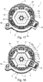
- Fig. 5 shows a view of the carrier 2 with the transistor boards 7 from a side facing the first region 6a of the carrier 2.
- the transistor boards 7 are arranged circulating and distributed about the centre axis 3 and fixed to the carrier ring 5 in a clamping or force-fit manner.
- two undercut fixing elements 21 and two clips 22 each are formed on the carrier ring 5 for the respective transistor board 7.
- the respective fixing elements 21 are arranged radially outside and the respective clips 22 are arranged radially inside.
- the same is slid with one side under the fixing elements 21 and on a side located opposite clipped to the carrier ring 5 via the clips 22.
- Fig. 6 now shows a view of the carrier 2 with the transistor boards 7 from a side facing the second region 6b of the carrier 2.
- Fig. 7 shows an enlarged extract from Fig. 6 .
- the carrier ring 5 comprises a contact opening 23 for the respective transistor board 7 so that contact points of the respective transistor board 7 are accessible from a side of the carrier ring 5 facing the second region 6b.
- the inverter 1 comprises multiple electrically conductive contact pins 24 which are cast into the carrier ring 5.
- the contact pins 24 are arranged about the contact opening 23 and electrically contacted with contact points of the respective transistor board 7 via an electrically conductive wire 25 each.
- the respective wire is wire bonded to the assigned contact point and the assigned contact pin 24.
- the respective contact pin 24 is L-shaped and extends in regions axially from the carrier ring 5 to the control circuit board 16.
- a thickened portion 26 facing the control circuit board 16 is formed, which then engages in a receiving opening 27 of the control circuit board 16 - see also Fig. 19 in this regard - and fixes the contact pin 24 in the control circuit board 16 in a clamping manner.
- the contact bus bars 18 arranged in the slots of the carrier ring 5 are electrically contacted with the circuit boards 7.
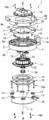
- Fig. 8 shows an exploded view
- Fig. 9 shows a view of the assembled state of the capacitor board 11, of the battery terminals 13 and of the screw assembly 13a.
- the battery terminals 13 are formed identically to one another and fastened in the centre on the capacitor board 11 by way of the screw assembly 13a.
- the respective battery terminal 13 is formed by a connector with a dielectric casing and electrically conductive lines located inside.
- the respective battery terminal 13 comprises altogether three pole contacts 28 which are electrically contacted with the capacitors 12 of the capacitor board 13 by means of an assigned screw of the screw assembly 13a each and via electrically conductive lines.
- the pole contacts 28 of the battery terminals 13 are arranged in a circle and centrally on the capacitor board 11.
- the capacitors 12 surround the pole contacts 28 of the battery terminals and are arranged symmetrically on the capacitor board 11.
- the one battery terminal 13 is assigned to the negative pole and the other battery terminal 13 is assigned to the positive pole.
- Fig. 10 now shows a view of the individual battery terminal 13.
- Fig. 11 and Fig. 12 show views of the battery terminals 13.
- the respective battery terminal 13 comprises a first bridge 29 that is parallel to the capacitor board 11 and a second bridge 29b that is parallel to the capacitor board 11.
- the first bridge 29a and the second bridge 29b are formed axially offset to one another.
- the respective bridge 29a or 29b connects two of the pole contacts 28 of the receptive battery terminal 13 to one another in an electrically conductive manner.
- the first bridge 29a of the one battery terminal 13 bridges the second bridge 29b of the other battery terminal 13, so that the pole contacts 28 of the battery terminals 13 are arranged in a circle and alternating one another in the circle.
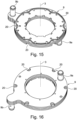
- Fig. 13 shows a view of the carrier 2 with the transistor boards 7 and the cooling plate 9 from a side facing the second region 6b of the carrier 2.
- the annular cooling plate 9 lies in the first region 6a of the carrier 2 against the transistor boards 7 in a heat-transferring manner.
- Fig. 14 shows a view of the cooling plate 9 with transistors 8 of the respective transistor boards 7.
- the transistor boards 7 are shown transparently for the sake of clarity.
- Fig. 15 shows a view of the cooling plate 9 from a side facing the carrier 2 and Fig. 16 shows a view of the cooling plate 9 from a side facing away from the carrier 2.
- the cooling plate 9 comprises the inlet 9a and the outlet 9b and can be flowed through by the cooling liquid.
- a circumferential groove 30 is additionally evident, in which the wall 4 of the carrier 2 is received in a form-fit and non-displaceable manner.
- Fig. 17 shows a view of the carrier 2 with the foam pad 14
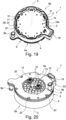
- Fig. 18 shows a view of the carrier 2 with the pressure plate 15 from a side facing the second region 6b of the carrier 2.
- the pressure plate 15 is connected to the cooling plate 9 through the carrier ring 5 by way of the screw assembly 15a and presses the foam pad 14 against the capacitor board 11 and the capacitor board 11 against contact bus bars 18. Because of this, the contact bus bars 18 are compressed between the transistor boards 7 and the capacitor board 11 and interconnect the transistor boards 7 and the capacitor board 11 in an electrically conductive manner.
- the iron cores 17 are arranged in receptacles 31 of the carrier ring 5.
- the receptacles 31 are provided for receiving phase terminals 35 of the electric motor 32.
- Fig. 19 shows a view of the carrier 2 with the control circuit board 16 from a side facing the second region 6b of the carrier 2.
- the thickened portions 26 of the contact pins 24 engage in the receiving openings 27 of the control circuit board 16, as a result of which the contact pins 24 are fixed in the control circuit board 16 in a force-fit manner.
- the control circuit board 16 is screwed to the pressure plate 15.
- Fig. 20 shows a view of the inverter 1 without the cover 10
- Fig. 21 shows a view of the inverter 1 with the cover 10 from a side facing the first region 6a of the carrier 2.
- the battery terminals 13 project through the carrier ring 5 and the cooling plate 9 axially to the outside and the capacitors 12 are arranged on the capacitor board 11 symmetrically about the battery terminals 13.
- the cover 10 is screwed to the cooling plate 9 by means of the screw assembly 10a and the battery terminals 13 project through the cover 10 to the outside.
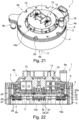
- Fig. 22 shows a sectional view of the inverter 1.
- the capacitor board 11 lies against the carrier ring 5 in the second region 6b of the carrier 2 and the capacitors 12 of the capacitor board 11 project through an opening of the carrier ring 5 into the first region 6a of the carrier 2.
- the pressure plate 15 is firmly connected to the cooling plate 9, so that the foam pad 14, the capacitor board 11, the contact bus bars 18, and the transistor boards 7 are pressed together i.e. are sandwiched between the pressure plate 15 and the cooling plate 9.
- the capacitor board 11 is pressed against the contact bus bars 18 by the foam pad 14 and the pressure plate 15.
- the transistor boards 7 are fixed on the carrier ring 5 in the first region 6a of the carrier 2 and distributed about the opening of the carrier ring 5 and thus about the capacitors 12.
- the contact bus bars 18 are compressed between the capacitor board 11 and the transistor boards 7 and because of this the transistor boards 7 and the capacitor board 11 are electrically contacted with one another.
- the battery terminals 13 are fastened centrally on the capacitor board 11 and project through the opening of the carrier ring 5 out of the second region 6b into the first region 6a of the carrier 2. Furthermore, the battery terminals are led through the cover 10 of the inverter axially to the outside.
- the control circuit board 16 is arranged in the second region 6b of the carrier 2 and screwed to the pressure plate 15. By way of the contact pins 24 in the carrier 2, the control circuit board 16 is electrically contacted with the transistor boards 7.
- Fig. 23 shows an exploded view
- Fig. 24 shows a sectional view of an electric motor 32 according to the invention.
- the electric motor 32 comprises a rotor 33 and a stator 34 which electromagnetically interact with one another.
- the rotor 33 is rotatable about an axis of rotation 43 which coincides with the centre axis 3 of the carrier 2 or inverter 1.
- the stator 34 comprises multiple coils 38 and a stator housing 36 which receives the coils 38.
- the rotor 33 is arranged in the stator 34 so that the coils 38 and the stator housing 36 encase the rotor 33.
- the inverter 1 is arranged axially to the stator 34 and connected to the stator housing 36 in a fixed manner by way of a screw assembly 36a.
- phase terminals 35 are distributed symmetrically about the axis of rotation 43 and arranged on assigned coil wires 37 radially outside.
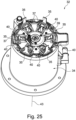
- Fig. 25 shows a view of the electric motor 32 without the inverter 1.
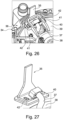
- Fig. 26 and Fig. 27 show views of the individual phase terminal 35 in the electric motor 32.
- the phase terminals 35 are arranged on the assigned coil wires 37 radially outside and are connected to these in an electrically conductive manner.
- the respective coil wire 37 engages radially in the respective phase terminal 35.
- the respective phase terminal 35 is L-shaped and, with a pressure ring 39, pressed against the stator 34 or against the stator housing 36.
- an elastically deformable support 40 each is arranged.
- the pressure ring 39 for the respective phase terminal 35 has two position projections 41.
- the position projections 41 engage in position openings 42 of the respective phase terminal 35, as a result of which the phase terminals 35 are fixed, correctly positioned, on the stator 34.
- the inverter 1 according to the invention can be finish-assembled independently of further elements of the electric motor 32. Because of this, both the effort and also the costs can be reduced. In addition, the inverter 1 can be electrically contacted with the stator 34 in a simplified and secure manner.
Landscapes
- Engineering & Computer Science (AREA)
- Power Engineering (AREA)
- Microelectronics & Electronic Packaging (AREA)
- Inverter Devices (AREA)
Claims (13)
- Wechselrichter (1) für einen Elektromotor (32),- wobei der Wechselrichter (1) eine Kondensatorplatine (11) umfasst, die mehrere Kondensatoren (12), mehrere Transistorplatinen (7) aufweist, die jeweils mehreren Transistoren (8) und eine Steuerplatine (16) aufweisen,- wobei die Kondensatorplatine (11), die jeweiligen Transistorplatinen (7) und die Steuerplatine (16) axial übereinander liegen und elektrisch miteinander verbunden sind,- wobei der Wechselrichter (1) für den Minuspol und für den Pluspol jeweils eine Batterieklemme (13) umfasst, welche mit der Kondensatorplatine (11) elektrisch leitend verbunden ist und axial aus der Kondensatorplatine (11) hervorsteht,- wobei die Batterieklemmen des Plus- und Minuspols (13) zueinander identisch sind und durch jeweils einen Steckverbinder jeweils mit einer äußeren dielektrischen Ummantelung, welche durch eine Abdeckung (10) des Wechselrichters (1) gebildet wird, und elektrisch leitfähigen Leitungen gebildet werden, welche sich im Inneren des Wechselrichters (1) befinden und aus der Abdeckung (10) zur Außenseite des Wechselrichters (1) hervorstehen,- wobei jede jeweilige Batterieklemme (13) drei Polkontakte (28) zum Kontaktieren mit der Kondensatorplatine (11) umfasst,- wobei die Kondensatoren (12) ringförmig auf der Kondensatorplatine (11) angeordnet sind,
dadurch gekennzeichnet,- dass die zwei Batterieklemmen (13) nebeneinander zwischen den Kondensatoren (12) und mittig auf der Kondensatorplatine (11) angeordnet sind, und- dass die Polkontakte (28) der einen Batterieklemme (13) und die Polkontakte (28) der anderen Batterieklemme (13) auf der Kondensatorplatine (11) in einem Kreis abwechselnd zueinander angeordnet sind. - Wechselrichter nach Anspruch 1, dadurch gekennzeichnet,
dass die Polkontakte (28) der Batterieklemmen (13) symmetrisch in der Mitte der Kondensatorplatine (11) angeordnet sind. - Wechselrichter nach Anspruch 1 oder 2,
dadurch gekennzeichnet,- dass die jeweilige Batterieklemme (13) eine erste Brücke (29a) umfasst, die parallel zur Kondensatorplatine (11) ist, welche den mittleren Polkontakt (28) mit dem einen seitlichen Polkontakt (28) elektrisch leitend verbindet, und- dass die jeweilige Batterieklemme (13) eine zweite Brücke (29b) umfasst, die parallel zur Kondensatorplatine (11) ist; welche den mittleren Polkontakt (28) mit dem anderen seitlichen Polkontakt (28) elektrisch leitend verbindet, und- dass die erste Brücke (29a) und die zweite Brücke (29b) in einem Winkel zueinander ausgerichtet und axial voneinander versetzt sind. - Wechselrichter nach Anspruch 3,
dadurch gekennzeichnet, dass in jedem Fall die erste Brücke (29a) der einen Batterieklemme (13) die zweite Brücke (29b) der anderen Batterieklemme (13) überbrückt, sodass die Polkontakte (28) der einen Batterieklemme (13) und die Polkontakte (28) der anderen Batterieklemme (13) in einem Kreis und abwechselnd zueinander angeordnet sind. - Wechselrichter nach einem der Ansprüche 2 bis 3,
dadurch gekennzeichnet, dass an einem der Polkontakte (28) der jeweiligen Batterieklemme (13) ein Kontaktverbinder gebildet ist, welcher axial aus der Kondensatorplatine (11) hervorsteht und nach außen führt, sodass über den Kontaktverbinder die Polkontakte (28) der jeweiligen Batterieklemme (13) nach außen elektrisch leitend kontaktierbar sind. - Wechselrichter nach einem der Ansprüche 1 bis 5,
dadurch gekennzeichnet,- dass der Wechselrichter (1) einen hohlzylindrischen Träger (2) mit einer Mittelachse (3) umfasst, welcher die Kondensatorplatine (11), die Transistorplatinen (7) und die Steuerplatine (16) trägt und dieselbe in der Umfangsrichtung nach außen umschließt, und- dass ein ringförmige Trägerring (5) in einem Stück in dem Träger (2) gebildet ist, und quer zu der Mittelachse (3) ausgerichtet ist, und- dass eine Druckplatte (15) fest mit einer Kühlplatte (9) verbunden ist, sodass ein elastisch verformbares Schaumstoffpolster (14), die Kondensatorplatine (11), der Trägerring (5) und die Transistorplatinen (7) zwischen der Druckplatte (15) und der Kühlplatte (9) zusammengepresst werden. - Wechselrichter nach Anspruch 6,
dadurch gekennzeichnet, dass die Batterieklemmen (13) durch eine Öffnung des ringförmigen Trägerrings (5) nach außen hervorstehen. - Wechselrichter nach Anspruch 6 oder 7,
dadurch gekennzeichnet, dass die Transistorplatinen (7) auf dem ringförmigen Trägerring (5) von der Kondensatorplatine (11) abgewandt und um die Mittelachse (3) umlaufend verteilt und klemmend befestigt sind. - Wechselrichter nach Anspruch 8,
dadurch gekennzeichnet,- dass in dem Trägerring (5) des Trägers (2) mehrere Kontaktstifte (24) eingegossen sind, welche axial von den Transistorplatinen (7) zu der Steuerplatine (16) ausgerichtet sind und um die Kondensatorplatine (11) umlaufen, und- dass die jeweilige Transistorplatine (7) über einen elektrisch leitenden Draht (25), welcher mit der jeweiligen Transistorplatine (7) und mit dem jeweiligen Kontaktstift (24) drahtgebunden ist, elektrisch mit dem jeweils zugeordneten Kontaktstift (24) kontaktiert ist, und- dass der jeweilige Kontaktstift (24) zu der Steuerplatine (16) hin jeweils einen endseitig verdickten Abschnitt (26) aufweist und die Steuerplatine (16) für den jeweiligen verdickten Abschnitt (26) eine Aufnahmeöffnung (27) umfasst, und- dass der jeweilige verdickte Abschnitt (26) in die jeweilige Aufnahmeöffnung (27) eingreift und hierdurch der jeweilige Kontaktstift (24) klemmend in der Steuerplatine (16) befestigt, und elektrisch mit der Steuerplatine (16) kontaktiert ist. - Wechselrichter nach einem der Ansprüche 6 bis 9,
dadurch gekennzeichnet,- dass an dem Trägerring (5) des Trägers (2) mehrere axiale Schlitze gebildet sind, in welchen jeweils eine Kontaktsammelschiene (18) aufgenommen ist, und- dass die jeweilige Kontaktsammelschiene (18) zwischen der jeweiligen Transistorplatine (7) und der Kondensatorplatine (11) zusammengedrückt ist, und deshalb die Transistorplatinen (7) mit der Kondensatorplatine (11) elektrisch kontaktiert sind. - Wechselrichter nach einem der Ansprüche 1 bis 10,
dadurch gekennzeichnet,- dass der Wechselrichter (1) eine ringförmige Kühlplatte (9) umfasst, durch die eine Kühlflüssigkeit fließen kann, welche wärmeübertragend an den Transistorplatinen (7) anliegt, und- dass die Kondensatoren (12) der Kondensatorplatine (11) axial zwischen den Transistorplatinen (7) und durch eine Öffnung der ringförmigen Kühlplatte (9) geführt sind und radial und wärmeübertragend an der Kühlplatte (9) anliegen, und- dass die Batterieklemmen (13) zwischen den Transistorplatinen (7) und zwischen den Kondensatoren (12) durch die Öffnung der ringförmigen Kühlplatte (9) axial nach außen hervorstehen. - Elektromotor (32),- wobei der Elektromotor (32) einen Rotor (33), der um eine Drehachse (43) drehbar ist, und einen Stator (34) umfasst, die elektromagnetisch miteinander zusammenwirken,- wobei der Stator (34) mehrere Statorspulen (38) umfasst, wobei zumindest einige der Statorspulen (38) über ihre Spulendrähte (37) elektrisch direkt mit drei elektrischen Phasen kontaktiert sind, und- wobei der Elektromotor (32) für die jeweilige Phase zumindest eine elektrisch leitende Phasenklemme (35) umfasst, welche mit dem zugeordneten Spulendraht (37) elektrisch leitend verbunden ist,dadurch gekennzeichnet,
dass der Elektromotor (32) den Wechselrichter (1) nach einem der vorstehenden Ansprüche umfasst, welcher den Phasenklemmen (35) zugewandt am Stator (34) befestigt ist, wobei die Phasenklemmen (35) in den Wechselrichter (1) eingreifen und elektrisch mit den Transistorplatinen (7) kontaktiert sind. - Motor nach Anspruch 12,
dadurch gekennzeichnet,- dass die jeweilige Phasenklemme (35) radial außerhalb des zugeordneten Spulendrahtes (37) liegt und der zugeordnete Spulendraht (37) deshalb radial in die jeweiligen Phasenklemme (35) eingreift, und- dass zwischen den jeweiligen Phasenklemmen (35) und dem Stator (34) jeweils eine elastisch verformbare Halterung (40) angeordnet ist und die jeweiligen Phasenklemmen (35) anhand eines Druckrings (39) gegen den Stator (34) gedrückt wird und über diesen an dem Stator (34) befestigt sind.
Priority Applications (1)
| Application Number | Priority Date | Filing Date | Title |
|---|---|---|---|
| EP20187148.0A EP3944477B1 (de) | 2020-07-22 | 2020-07-22 | Wechselrichter und elektromotor mit einem solchen wechselrichter |
Applications Claiming Priority (1)
| Application Number | Priority Date | Filing Date | Title |
|---|---|---|---|
| EP20187148.0A EP3944477B1 (de) | 2020-07-22 | 2020-07-22 | Wechselrichter und elektromotor mit einem solchen wechselrichter |
Publications (2)
| Publication Number | Publication Date |
|---|---|
| EP3944477A1 EP3944477A1 (de) | 2022-01-26 |
| EP3944477B1 true EP3944477B1 (de) | 2024-09-18 |
Family
ID=71741672
Family Applications (1)
| Application Number | Title | Priority Date | Filing Date |
|---|---|---|---|
| EP20187148.0A Active EP3944477B1 (de) | 2020-07-22 | 2020-07-22 | Wechselrichter und elektromotor mit einem solchen wechselrichter |
Country Status (1)
| Country | Link |
|---|---|
| EP (1) | EP3944477B1 (de) |
Family Cites Families (7)
| Publication number | Priority date | Publication date | Assignee | Title |
|---|---|---|---|---|
| DE10220047A1 (de) * | 2002-05-04 | 2003-11-20 | Jungheinrich Ag | Antriebssystem mit Umrichtersteuerung für Niederspannungs-Drehstrommotoren |
| JP5118548B2 (ja) | 2007-05-14 | 2013-01-16 | アスモ株式会社 | モータ |
| JP5708583B2 (ja) * | 2012-07-12 | 2015-04-30 | 株式会社豊田自動織機 | インバータ装置 |
| JP6303522B2 (ja) * | 2014-01-17 | 2018-04-04 | 株式会社豊田自動織機 | 半導体装置 |
| JP6343210B2 (ja) | 2014-09-03 | 2018-06-13 | 日立オートモティブシステムズ株式会社 | 電動駆動装置及び電動パワーステアリング装置 |
| JP6522358B2 (ja) | 2015-02-09 | 2019-05-29 | 日立オートモティブシステムズ株式会社 | 電動駆動装置及び電動パワーステアリング装置 |
| EP3609066B1 (de) * | 2018-08-07 | 2021-02-24 | Mahle International GmbH | Stromwechselrichter |
-
2020
- 2020-07-22 EP EP20187148.0A patent/EP3944477B1/de active Active
Also Published As
| Publication number | Publication date |
|---|---|
| EP3944477A1 (de) | 2022-01-26 |
Similar Documents
| Publication | Publication Date | Title |
|---|---|---|
| US11509196B2 (en) | Motor vehicle and power converter device for a motor vehicle | |
| US6992409B2 (en) | Liquid-cooled rotary electric machine integrated with an inverter | |
| CN111108668B (zh) | 电动助力转向装置 | |
| KR102466610B1 (ko) | 제어기 및 이를 포함하는 모터 조립체 | |
| CN101185227A (zh) | 用于旋转电气设备的电子模块 | |
| US12334798B2 (en) | Inverter for an electric motor | |
| CN101185226B (zh) | 用于旋转电气设备的电子部件组件 | |
| US10263495B2 (en) | Rotary electric machine | |
| EP3944476B1 (de) | Wechselrichter und elektromotor mit einem solchen wechselrichter | |
| RU2661907C1 (ru) | Блок контактных выводов вращающейся электрической машины | |
| EP3944469B1 (de) | Elektromotor | |
| KR102504424B1 (ko) | 모터용 제어기 및 이를 포함하는 모터 조립체 | |
| EP3944477B1 (de) | Wechselrichter und elektromotor mit einem solchen wechselrichter | |
| EP3306792A1 (de) | Halbleiterbauelement | |
| CN111817471A (zh) | 用于三相电动马达的定子 | |
| EP4102713A1 (de) | Wechselrichter und motor mit dem wechselrichter | |
| JP7778235B2 (ja) | 回転電機ユニット | |
| CN107769441B (zh) | 电机 | |
| JP7042943B1 (ja) | 回転電機 | |
| KR102466611B1 (ko) | 제어기 및 이를 포함하는 모터 조립체 | |
| JP7706657B2 (ja) | 回転電機ユニット | |
| US6958558B2 (en) | Electric motor in particular for a steering system in a vehicle | |
| CN111817470A (zh) | 用于三相电动马达的定子 | |
| JP2023154697A (ja) | 回転電機ユニット | |
| JP7361891B2 (ja) | 回転電機 |
Legal Events
| Date | Code | Title | Description |
|---|---|---|---|
| PUAI | Public reference made under article 153(3) epc to a published international application that has entered the european phase |
Free format text: ORIGINAL CODE: 0009012 |
|
| STAA | Information on the status of an ep patent application or granted ep patent |
Free format text: STATUS: THE APPLICATION HAS BEEN PUBLISHED |
|
| AK | Designated contracting states |
Kind code of ref document: A1 Designated state(s): AL AT BE BG CH CY CZ DE DK EE ES FI FR GB GR HR HU IE IS IT LI LT LU LV MC MK MT NL NO PL PT RO RS SE SI SK SM TR |
|
| STAA | Information on the status of an ep patent application or granted ep patent |
Free format text: STATUS: REQUEST FOR EXAMINATION WAS MADE |
|
| 17P | Request for examination filed |
Effective date: 20220317 |
|
| RBV | Designated contracting states (corrected) |
Designated state(s): AL AT BE BG CH CY CZ DE DK EE ES FI FR GB GR HR HU IE IS IT LI LT LU LV MC MK MT NL NO PL PT RO RS SE SI SK SM TR |
|
| STAA | Information on the status of an ep patent application or granted ep patent |
Free format text: STATUS: EXAMINATION IS IN PROGRESS |
|
| 17Q | First examination report despatched |
Effective date: 20230519 |
|
| GRAP | Despatch of communication of intention to grant a patent |
Free format text: ORIGINAL CODE: EPIDOSNIGR1 |
|
| RIC1 | Information provided on ipc code assigned before grant |
Ipc: H02K 9/197 20060101ALN20240322BHEP Ipc: H01R 11/09 20060101ALN20240322BHEP Ipc: H02K 9/19 20060101ALN20240322BHEP Ipc: H02K 5/20 20060101ALN20240322BHEP Ipc: H02K 11/05 20160101ALI20240322BHEP Ipc: H01R 4/30 20060101ALI20240322BHEP Ipc: H02K 5/22 20060101ALI20240322BHEP Ipc: H02K 11/33 20160101AFI20240322BHEP |
|
| STAA | Information on the status of an ep patent application or granted ep patent |
Free format text: STATUS: GRANT OF PATENT IS INTENDED |
|
| RIC1 | Information provided on ipc code assigned before grant |
Ipc: H02K 9/197 20060101ALN20240416BHEP Ipc: H01R 11/09 20060101ALN20240416BHEP Ipc: H02K 9/19 20060101ALN20240416BHEP Ipc: H02K 5/20 20060101ALN20240416BHEP Ipc: H02K 11/05 20160101ALI20240416BHEP Ipc: H01R 4/30 20060101ALI20240416BHEP Ipc: H02K 5/22 20060101ALI20240416BHEP Ipc: H02K 11/33 20160101AFI20240416BHEP |
|
| INTG | Intention to grant announced |
Effective date: 20240502 |
|
| GRAS | Grant fee paid |
Free format text: ORIGINAL CODE: EPIDOSNIGR3 |
|
| GRAA | (expected) grant |
Free format text: ORIGINAL CODE: 0009210 |
|
| STAA | Information on the status of an ep patent application or granted ep patent |
Free format text: STATUS: THE PATENT HAS BEEN GRANTED |
|
| AK | Designated contracting states |
Kind code of ref document: B1 Designated state(s): AL AT BE BG CH CY CZ DE DK EE ES FI FR GB GR HR HU IE IS IT LI LT LU LV MC MK MT NL NO PL PT RO RS SE SI SK SM TR |
|
| REG | Reference to a national code |
Ref country code: GB Ref legal event code: FG4D |
|
| REG | Reference to a national code |
Ref country code: CH Ref legal event code: EP |
|
| REG | Reference to a national code |
Ref country code: IE Ref legal event code: FG4D |
|
| REG | Reference to a national code |
Ref country code: DE Ref legal event code: R096 Ref document number: 602020037819 Country of ref document: DE |
|
| REG | Reference to a national code |
Ref country code: LT Ref legal event code: MG9D |
|
| PG25 | Lapsed in a contracting state [announced via postgrant information from national office to epo] |
Ref country code: NO Free format text: LAPSE BECAUSE OF FAILURE TO SUBMIT A TRANSLATION OF THE DESCRIPTION OR TO PAY THE FEE WITHIN THE PRESCRIBED TIME-LIMIT Effective date: 20241218 |
|
| PG25 | Lapsed in a contracting state [announced via postgrant information from national office to epo] |
Ref country code: GR Free format text: LAPSE BECAUSE OF FAILURE TO SUBMIT A TRANSLATION OF THE DESCRIPTION OR TO PAY THE FEE WITHIN THE PRESCRIBED TIME-LIMIT Effective date: 20241219 Ref country code: FI Free format text: LAPSE BECAUSE OF FAILURE TO SUBMIT A TRANSLATION OF THE DESCRIPTION OR TO PAY THE FEE WITHIN THE PRESCRIBED TIME-LIMIT Effective date: 20240918 |
|
| PG25 | Lapsed in a contracting state [announced via postgrant information from national office to epo] |
Ref country code: BG Free format text: LAPSE BECAUSE OF FAILURE TO SUBMIT A TRANSLATION OF THE DESCRIPTION OR TO PAY THE FEE WITHIN THE PRESCRIBED TIME-LIMIT Effective date: 20240918 |
|
| PG25 | Lapsed in a contracting state [announced via postgrant information from national office to epo] |
Ref country code: LV Free format text: LAPSE BECAUSE OF FAILURE TO SUBMIT A TRANSLATION OF THE DESCRIPTION OR TO PAY THE FEE WITHIN THE PRESCRIBED TIME-LIMIT Effective date: 20240918 |
|
| PG25 | Lapsed in a contracting state [announced via postgrant information from national office to epo] |
Ref country code: HR Free format text: LAPSE BECAUSE OF FAILURE TO SUBMIT A TRANSLATION OF THE DESCRIPTION OR TO PAY THE FEE WITHIN THE PRESCRIBED TIME-LIMIT Effective date: 20240918 |
|
| REG | Reference to a national code |
Ref country code: NL Ref legal event code: MP Effective date: 20240918 |
|
| PG25 | Lapsed in a contracting state [announced via postgrant information from national office to epo] |
Ref country code: RS Free format text: LAPSE BECAUSE OF FAILURE TO SUBMIT A TRANSLATION OF THE DESCRIPTION OR TO PAY THE FEE WITHIN THE PRESCRIBED TIME-LIMIT Effective date: 20241218 |
|
| PG25 | Lapsed in a contracting state [announced via postgrant information from national office to epo] |
Ref country code: RS Free format text: LAPSE BECAUSE OF FAILURE TO SUBMIT A TRANSLATION OF THE DESCRIPTION OR TO PAY THE FEE WITHIN THE PRESCRIBED TIME-LIMIT Effective date: 20241218 Ref country code: NO Free format text: LAPSE BECAUSE OF FAILURE TO SUBMIT A TRANSLATION OF THE DESCRIPTION OR TO PAY THE FEE WITHIN THE PRESCRIBED TIME-LIMIT Effective date: 20241218 Ref country code: LV Free format text: LAPSE BECAUSE OF FAILURE TO SUBMIT A TRANSLATION OF THE DESCRIPTION OR TO PAY THE FEE WITHIN THE PRESCRIBED TIME-LIMIT Effective date: 20240918 Ref country code: HR Free format text: LAPSE BECAUSE OF FAILURE TO SUBMIT A TRANSLATION OF THE DESCRIPTION OR TO PAY THE FEE WITHIN THE PRESCRIBED TIME-LIMIT Effective date: 20240918 Ref country code: GR Free format text: LAPSE BECAUSE OF FAILURE TO SUBMIT A TRANSLATION OF THE DESCRIPTION OR TO PAY THE FEE WITHIN THE PRESCRIBED TIME-LIMIT Effective date: 20241219 Ref country code: FI Free format text: LAPSE BECAUSE OF FAILURE TO SUBMIT A TRANSLATION OF THE DESCRIPTION OR TO PAY THE FEE WITHIN THE PRESCRIBED TIME-LIMIT Effective date: 20240918 Ref country code: BG Free format text: LAPSE BECAUSE OF FAILURE TO SUBMIT A TRANSLATION OF THE DESCRIPTION OR TO PAY THE FEE WITHIN THE PRESCRIBED TIME-LIMIT Effective date: 20240918 |
|
| REG | Reference to a national code |
Ref country code: AT Ref legal event code: MK05 Ref document number: 1725518 Country of ref document: AT Kind code of ref document: T Effective date: 20240918 |
|
| PG25 | Lapsed in a contracting state [announced via postgrant information from national office to epo] |
Ref country code: NL Free format text: LAPSE BECAUSE OF FAILURE TO SUBMIT A TRANSLATION OF THE DESCRIPTION OR TO PAY THE FEE WITHIN THE PRESCRIBED TIME-LIMIT Effective date: 20240918 |
|
| PG25 | Lapsed in a contracting state [announced via postgrant information from national office to epo] |
Ref country code: PT Free format text: LAPSE BECAUSE OF FAILURE TO SUBMIT A TRANSLATION OF THE DESCRIPTION OR TO PAY THE FEE WITHIN THE PRESCRIBED TIME-LIMIT Effective date: 20250120 Ref country code: IS Free format text: LAPSE BECAUSE OF FAILURE TO SUBMIT A TRANSLATION OF THE DESCRIPTION OR TO PAY THE FEE WITHIN THE PRESCRIBED TIME-LIMIT Effective date: 20250118 |
|
| PG25 | Lapsed in a contracting state [announced via postgrant information from national office to epo] |
Ref country code: SM Free format text: LAPSE BECAUSE OF FAILURE TO SUBMIT A TRANSLATION OF THE DESCRIPTION OR TO PAY THE FEE WITHIN THE PRESCRIBED TIME-LIMIT Effective date: 20240918 Ref country code: RO Free format text: LAPSE BECAUSE OF FAILURE TO SUBMIT A TRANSLATION OF THE DESCRIPTION OR TO PAY THE FEE WITHIN THE PRESCRIBED TIME-LIMIT Effective date: 20240918 |
|
| PG25 | Lapsed in a contracting state [announced via postgrant information from national office to epo] |
Ref country code: ES Free format text: LAPSE BECAUSE OF FAILURE TO SUBMIT A TRANSLATION OF THE DESCRIPTION OR TO PAY THE FEE WITHIN THE PRESCRIBED TIME-LIMIT Effective date: 20240918 |
|
| PG25 | Lapsed in a contracting state [announced via postgrant information from national office to epo] |
Ref country code: EE Free format text: LAPSE BECAUSE OF FAILURE TO SUBMIT A TRANSLATION OF THE DESCRIPTION OR TO PAY THE FEE WITHIN THE PRESCRIBED TIME-LIMIT Effective date: 20240918 Ref country code: AT Free format text: LAPSE BECAUSE OF FAILURE TO SUBMIT A TRANSLATION OF THE DESCRIPTION OR TO PAY THE FEE WITHIN THE PRESCRIBED TIME-LIMIT Effective date: 20240918 |
|
| PG25 | Lapsed in a contracting state [announced via postgrant information from national office to epo] |
Ref country code: CZ Free format text: LAPSE BECAUSE OF FAILURE TO SUBMIT A TRANSLATION OF THE DESCRIPTION OR TO PAY THE FEE WITHIN THE PRESCRIBED TIME-LIMIT Effective date: 20240918 Ref country code: PL Free format text: LAPSE BECAUSE OF FAILURE TO SUBMIT A TRANSLATION OF THE DESCRIPTION OR TO PAY THE FEE WITHIN THE PRESCRIBED TIME-LIMIT Effective date: 20240918 |
|
| PG25 | Lapsed in a contracting state [announced via postgrant information from national office to epo] |
Ref country code: SK Free format text: LAPSE BECAUSE OF FAILURE TO SUBMIT A TRANSLATION OF THE DESCRIPTION OR TO PAY THE FEE WITHIN THE PRESCRIBED TIME-LIMIT Effective date: 20240918 Ref country code: IT Free format text: LAPSE BECAUSE OF FAILURE TO SUBMIT A TRANSLATION OF THE DESCRIPTION OR TO PAY THE FEE WITHIN THE PRESCRIBED TIME-LIMIT Effective date: 20240918 |
|
| REG | Reference to a national code |
Ref country code: DE Ref legal event code: R097 Ref document number: 602020037819 Country of ref document: DE |
|
| PG25 | Lapsed in a contracting state [announced via postgrant information from national office to epo] |
Ref country code: DK Free format text: LAPSE BECAUSE OF FAILURE TO SUBMIT A TRANSLATION OF THE DESCRIPTION OR TO PAY THE FEE WITHIN THE PRESCRIBED TIME-LIMIT Effective date: 20240918 |
|
| PLBE | No opposition filed within time limit |
Free format text: ORIGINAL CODE: 0009261 |
|
| STAA | Information on the status of an ep patent application or granted ep patent |
Free format text: STATUS: NO OPPOSITION FILED WITHIN TIME LIMIT |
|
| 26N | No opposition filed |
Effective date: 20250619 |
|
| PG25 | Lapsed in a contracting state [announced via postgrant information from national office to epo] |
Ref country code: SE Free format text: LAPSE BECAUSE OF FAILURE TO SUBMIT A TRANSLATION OF THE DESCRIPTION OR TO PAY THE FEE WITHIN THE PRESCRIBED TIME-LIMIT Effective date: 20240918 |
|
| PGFP | Annual fee paid to national office [announced via postgrant information from national office to epo] |
Ref country code: DE Payment date: 20250722 Year of fee payment: 6 |
|
| P01 | Opt-out of the competence of the unified patent court (upc) registered |
Free format text: CASE NUMBER: UPC_APP_8059_3944477/2025 Effective date: 20250926 |
|
| REG | Reference to a national code |
Ref country code: CH Ref legal event code: H13 Free format text: ST27 STATUS EVENT CODE: U-0-0-H10-H13 (AS PROVIDED BY THE NATIONAL OFFICE) Effective date: 20260224 |
|
| PG25 | Lapsed in a contracting state [announced via postgrant information from national office to epo] |
Ref country code: LU Free format text: LAPSE BECAUSE OF NON-PAYMENT OF DUE FEES Effective date: 20250722 |
|
| GBPC | Gb: european patent ceased through non-payment of renewal fee |
Effective date: 20250722 |
|
| REG | Reference to a national code |
Ref country code: BE Ref legal event code: MM Effective date: 20250731 |
|
| PG25 | Lapsed in a contracting state [announced via postgrant information from national office to epo] |
Ref country code: GB Free format text: LAPSE BECAUSE OF NON-PAYMENT OF DUE FEES Effective date: 20250722 |
|
| PG25 | Lapsed in a contracting state [announced via postgrant information from national office to epo] |
Ref country code: BE Free format text: LAPSE BECAUSE OF NON-PAYMENT OF DUE FEES Effective date: 20250731 |
|
| PG25 | Lapsed in a contracting state [announced via postgrant information from national office to epo] |
Ref country code: FR Free format text: LAPSE BECAUSE OF NON-PAYMENT OF DUE FEES Effective date: 20250731 |