EP3944342B1 - Verfahren zum verbinden von photovoltaischen zellen und dadurch herstellbare photovoltaische zellenanordnung - Google Patents
Verfahren zum verbinden von photovoltaischen zellen und dadurch herstellbare photovoltaische zellenanordnung Download PDFInfo
- Publication number
- EP3944342B1 EP3944342B1 EP20187110.0A EP20187110A EP3944342B1 EP 3944342 B1 EP3944342 B1 EP 3944342B1 EP 20187110 A EP20187110 A EP 20187110A EP 3944342 B1 EP3944342 B1 EP 3944342B1
- Authority
- EP
- European Patent Office
- Prior art keywords
- cell
- photovoltaic cell
- edge
- photovoltaic
- wire
- Prior art date
- Legal status (The legal status is an assumption and is not a legal conclusion. Google has not performed a legal analysis and makes no representation as to the accuracy of the status listed.)
- Active
Links
Images





Classifications
-
- H—ELECTRICITY
- H10—SEMICONDUCTOR DEVICES; ELECTRIC SOLID-STATE DEVICES NOT OTHERWISE PROVIDED FOR
- H10F—INORGANIC SEMICONDUCTOR DEVICES SENSITIVE TO INFRARED RADIATION, LIGHT, ELECTROMAGNETIC RADIATION OF SHORTER WAVELENGTH OR CORPUSCULAR RADIATION
- H10F71/00—Manufacture or treatment of devices covered by this subclass
- H10F71/137—Batch treatment of the devices
- H10F71/1375—Apparatus for automatic interconnection of photovoltaic cells in a module
-
- H—ELECTRICITY
- H10—SEMICONDUCTOR DEVICES; ELECTRIC SOLID-STATE DEVICES NOT OTHERWISE PROVIDED FOR
- H10F—INORGANIC SEMICONDUCTOR DEVICES SENSITIVE TO INFRARED RADIATION, LIGHT, ELECTROMAGNETIC RADIATION OF SHORTER WAVELENGTH OR CORPUSCULAR RADIATION
- H10F10/00—Individual photovoltaic cells, e.g. solar cells
- H10F10/10—Individual photovoltaic cells, e.g. solar cells having potential barriers
- H10F10/16—Photovoltaic cells having only PN heterojunction potential barriers
- H10F10/167—Photovoltaic cells having only PN heterojunction potential barriers comprising Group I-III-VI materials, e.g. CdS/CuInSe2 [CIS] heterojunction photovoltaic cells
-
- H—ELECTRICITY
- H10—SEMICONDUCTOR DEVICES; ELECTRIC SOLID-STATE DEVICES NOT OTHERWISE PROVIDED FOR
- H10F—INORGANIC SEMICONDUCTOR DEVICES SENSITIVE TO INFRARED RADIATION, LIGHT, ELECTROMAGNETIC RADIATION OF SHORTER WAVELENGTH OR CORPUSCULAR RADIATION
- H10F19/00—Integrated devices, or assemblies of multiple devices, comprising at least one photovoltaic cell covered by group H10F10/00, e.g. photovoltaic modules
- H10F19/90—Structures for connecting between photovoltaic cells, e.g. interconnections or insulating spacers
- H10F19/902—Structures for connecting between photovoltaic cells, e.g. interconnections or insulating spacers for series or parallel connection of photovoltaic cells
- H10F19/904—Structures for connecting between photovoltaic cells, e.g. interconnections or insulating spacers for series or parallel connection of photovoltaic cells characterised by the shapes of the structures
-
- H—ELECTRICITY
- H10—SEMICONDUCTOR DEVICES; ELECTRIC SOLID-STATE DEVICES NOT OTHERWISE PROVIDED FOR
- H10F—INORGANIC SEMICONDUCTOR DEVICES SENSITIVE TO INFRARED RADIATION, LIGHT, ELECTROMAGNETIC RADIATION OF SHORTER WAVELENGTH OR CORPUSCULAR RADIATION
- H10F19/00—Integrated devices, or assemblies of multiple devices, comprising at least one photovoltaic cell covered by group H10F10/00, e.g. photovoltaic modules
- H10F19/90—Structures for connecting between photovoltaic cells, e.g. interconnections or insulating spacers
- H10F19/902—Structures for connecting between photovoltaic cells, e.g. interconnections or insulating spacers for series or parallel connection of photovoltaic cells
- H10F19/906—Structures for connecting between photovoltaic cells, e.g. interconnections or insulating spacers for series or parallel connection of photovoltaic cells characterised by the materials of the structures
-
- Y—GENERAL TAGGING OF NEW TECHNOLOGICAL DEVELOPMENTS; GENERAL TAGGING OF CROSS-SECTIONAL TECHNOLOGIES SPANNING OVER SEVERAL SECTIONS OF THE IPC; TECHNICAL SUBJECTS COVERED BY FORMER USPC CROSS-REFERENCE ART COLLECTIONS [XRACs] AND DIGESTS
- Y02—TECHNOLOGIES OR APPLICATIONS FOR MITIGATION OR ADAPTATION AGAINST CLIMATE CHANGE
- Y02E—REDUCTION OF GREENHOUSE GAS [GHG] EMISSIONS, RELATED TO ENERGY GENERATION, TRANSMISSION OR DISTRIBUTION
- Y02E10/00—Energy generation through renewable energy sources
- Y02E10/50—Photovoltaic [PV] energy
- Y02E10/541—CuInSe2 material PV cells
Definitions
- the invention relates to a method for interconnecting photovoltaic cells in order to form a photovoltaic cells assembly and a photovoltaic cells assembly being producible by the steps of said method.
- DE 10 2009 035 703 A1 relates to a method for generation of a system of flexible thin-film solar cells by electrically connecting individual cells or cell complexes. Said method involves piercing the thin-film solar cells from the front side through the carrier in a narrow region. An electrically conductive wire covered with an insulating coating is guided through the formed openings. In other words, the thin-film solar cells are sewn using the covered and thus electrically insulated wire. In addition to this, the insulating coating of the electrically conductive wire is etched locally to enable the formation of an electrical connection between the wire and contacts of the thin-film solar cells.
- US 2010/131108 A1 relates to a method of interconnecting solar cells whereby the conductive wire is used as stitching yarn to interconnect adjacent cells.
- Said method comprises the steps of providing a first photovoltaic cell comprising a first surface, a second surface, a first edge, and a second edge, arranging a conductive wire on the first surface of the first photovoltaic cell according to a certain pattern, and attaching the conductive wire to the first surface of the first photovoltaic cell with the aid of a first non-conductive yarn by stitching in an area of the first edge of the first photovoltaic cell according to a first stitch type.
- the method for interconnecting photovoltaic cells especially establishes an interconnection between the photovoltaic cells.
- a risk of breakage of the conductive wire is reduced, and consequently a risk of loss of electrical connections negatively affecting the device performance is reduced.
- the first edge may especially be opposing the second edge.
- the conductive wire it is noted that the conductive wire is an electrically conductive wire.
- the first non-conductive yarn it is noted that the first non-conductive yarn is a first electrically non-conductive yarn.
- the interconnection may especially be an electrical interconnection.
- attaching the conductive wire to the first surface of the first photovoltaic cell may comprise connecting, especially electrically connecting, the conductive wire to a contact structure or a contact layer on the first surface of the first photovoltaic cell, thereby preferably establishing a contact, especially an electrical contact between the conductive wire and the contact structure or contact layer.
- an electrical connection between the conductive wire and the contact structure or contact layer of the first photovoltaic cell can be established without any complex process steps, such as, for example, without the need for locally removing an insulating coating from the conductive wire. Therefore, a relatively simple process is provided with a reduced number of process steps, which leads to reduced manufacturing costs.
- first non-conductive yarn may be stitched especially through the first photovoltaic cell.
- the method comprises the step of additionally attaching the conductive wire to the first surface of the first photovoltaic cell with the aid of a second non-conductive yarn by stitching in an area of the second edge of the first photovoltaic cell according to a second stitch type.
- the probability of defects especially due to incorrect interconnections can further be reduced by accurately attaching the wire.
- the second non-conductive yarn may be stitched especially through the first photovoltaic cell.
- the second stitch type is equal to the first stitch type.
- the first stitch type may be equal to the second stitch type.
- stitching according to the second stitch type is configured to pull a loop being fed through a hole in the first photovoltaic cell with the aid of the second non-conductive yarn over an edge, preferably the second edge, of the first photovoltaic cell especially along the second surface of the first photovoltaic cell.
- the second stitch type comprises or is an ISO #501 stitch or an over-edge stitch or an overlock stitch or an over-edge chainstitch, preferably a one-thread over-edge chainstitch.
- the second non-conductive yarn is preferably wrapped around the second edge of the first photovoltaic cell. This may thereby also separate and isolate, especially electrically isolate, in a later stage the second edge of the first photovoltaic cell from a first edge of a further photovoltaic cell to be provided next to it.
- the second stitch type may comprise or be an ISO #101 stitch or a chainstitch.
- the first photovoltaic cell comprises or is a thin-film cell, preferably a chalcogenide cell such as e.g. a CdTe (Cadmium Telluride) cell, a CIS (Copper Indium Selenide) cell, a CGS (Copper Gallium Selenide) cell, a CIGS (Copper Indium Gallium Selenide, Copper Indium Gallium Sulfide) cell, a kesterite cell such as a CZTS (Copper Zinc Tin Sulfide, Copper Zinc Tin Selenide) cell, a perovskite cell, an amorphous silicon cell, a microcrystalline silicon cell, a polycrystalline cell or an organic cell .
- a chalcogenide cell such as e.g. a CdTe (Cadmium Telluride) cell, a CIS (Copper Indium Selenide) cell, a CGS (Copper Gallium Selenide) cell, a CIGS (Copper Indium Gallium Sel
- the first edge and the second edge are parallel or approximately parallel with respect to each other.
- the conductive wire comprises at least one of copper, nickel, steel, stainless steel, aluminum, carbon fiber, or any combination thereof.
- the certain pattern comprises at least one of a zig-zag pattern, a sine-shaped pattern, a pattern being similar to a sine shape, or any combination thereof.
- nickel may be preferred.
- said pattern may additionally or alternatively comprise a plurality of straight lines (e.g., parallel to each other).
- arranging the conductive wire on the first surface of the cell would preferably not be done with a swinging arm or swinging beam.
- a swinging arm or beam, respectively will be shown and explained below.
- a possible approach would for example be to provide a plurality of wires (e.g.
- this second cell may be provided on the part of the wires that extends beyond the second edge of the first cell (especially for series connection of the cell).
- said approach with a plurality of parallel wires would also be suitable for parallel interconnection of subsequent cells.
- a first plurality of wires could be provided underneath the cells and a second plurality of wires could be provided on top of the cells (such that, in the end, all first surfaces are connected at one hand, and all second surfaces are connected at the other hand).
- a first plurality of wires could be provided underneath the cells and a second plurality of wires could be provided on top of the cells (such that, in the end, all first surfaces are connected at one hand, and all second surfaces are connected at the other hand).
- the first non-conductive yarn comprises at least one of polyolefin, nylon, or the combination thereof.
- the second non-conductive yarn comprises at least one of polyolefin, nylon, or the combination thereof.
- steel foil may preferably be used for making the copper indium gallium selenide cell especially by depositing active copper indium gallium selenide layers on the surface.
- polyolefin may be more preferred than nylon.
- the diameter of the first and/or the second non-conductive yarn may especially be between 50 and 300 micrometers, preferably between 100 and 200 micrometers.
- the conductive wire comprises carbon fiber
- the conductive wire may preferably be a conductive yarn.
- the conductive wires or conductive yarns can be coated.
- the respective coatings may comprise at least one of Sn, Bi, Ag, Pb, In, Co, Cu, Ni, Zn, or any combination thereof.
- a Cu- or Al-wire with such solderable coating may preferably be used.
- the diameter of the conductive wire may especially be between 20 and 400 micrometers, preferably between 40 and 200 micrometers, more preferably between 60 and 120 micrometers.
- the corresponding contact pad or contact structure deposited on the solar cell may comprise at least one of Sn, Bi, Ag, Pb, In, Co, Cu, Ni, Zn, or any combination thereof especially in order to create a metallurgical contact with the wire or yarn, respectively.
- an electrically conductive adhesive paste may be printed on the respective cell, or coated on the respective wires and/or yarns to create an electrical contact with a contact layer of the cell.
- the electrically conductive adhesive may be an isotropic conductive adhesive or an anisotropic conductive adhesive.
- a Cu-wire with Ni-coating may preferably be used.
- a heating step may be performed, for example, at a temperature in the range between 60 and 200 degrees Celsius, preferably at a temperature in the range between 100 and 180 degrees Celsius.
- This heating step may be done just after having attached the conductive wire or yarn on the cell surface or it may be done later in the process, such as, for example, after having formed a photovoltaic cells assembly (as further described), or simultaneously with a heating step performed for encapsulation of the photovoltaic cells assembly (as further described).
- a dedicated, separate heating step to establish the electrical connection, resulting in a reduction of the number of process steps and thus an efficient manufacturing process.
- said yarns may especially comprise an optically transparent material such as polyolefin or a material such as nylon.
- an optically transparent material such as polyolefin or a material such as nylon.
- the usage of the optically transparent material is preferred.
- conductive substrates preferably electrically conductive substrates
- said conductive substrate may especially comprise or be a foil or a sheet, preferably a metal foil or a metal sheet.
- said foil or sheet may especially comprise at least one of copper, steel, preferably stainless steel, nickel, preferably steel nickel, aluminum, or any combination thereof.
- the foil or sheet may comprise a coating, preferably a metal coating.
- said coating may comprise at least one of Mo, Ag, Cu, Ni, Sn, Bi, Co, or any combination thereof.
- such a layer stack especially for copper indium gallium selenide cells and/or a copper indium selenide cells may comprise at least one of a first layer, preferably a front contact layer, comprising Al-doped ZnO or ITO, a second layer, preferably a window layer, comprising ZnO, preferably intrinsic ZnO, a third layer, preferably buffer layer or a n-type buffer layer, comprising CdS and/or ZnO and/or InO and/or ZnOS and/or InS, a fourth layer, preferably an absorber layer or a p-type absorber layer, a fifth layer, preferably a back contact layer, comprising Mo, a sixth layer, preferably a substrate layer such as the above-mentioned substrates, or any combination thereof.
- a first layer preferably a front contact layer, comprising Al-doped ZnO or ITO
- a second layer preferably a window layer, comprising ZnO, preferably intrinsic ZnO
- said sixth layer or substrate layer may especially be a stainless-steel substrate, such as a stainless-steel substrate with a Mo coating.
- Said stainless-steel substrate may preferably be between 30 and 150 micrometers, more preferably between 50 and 130 micrometers, thick.
- the top of the respective cell may especially be the first layer, whereas the bottom of the respective cell may especially be the sixth layer. Accordingly, the remaining layers may be sandwiched by the top and the bottom layer of the respective cell.
- the top of the cell may be the front side of the cell, i.e. the side of the cell adapted for being oriented towards a light source and thus for receiving illumination.
- the bottom of the cell may be the rear side or back side of the cell, i.e. the side opposite to the front side.
- a swinging arm or beam is used for arranging the conductive wire.
- a respective machine stitching presser foot and a corresponding needle are used for stitching.
- complexity can further be reduced and manufacturing may be done in an automated way, which leads to an increased cost-efficiency.
- said swinging arm or beam may comprise or be a device being configured to feed the conductive wire and/or to arrange the conductive wire on the surface in a zigzag and/or sine-shaped movement/pattern, being preferably combined with two sewing presser feet. It is noted that a possible way to arrange the wire in this way is a swinging arm or beam, but it is not limited to this.
- the conductive wire is arranged in such a manner that at least a part, preferably a wire loop or a wire loop pattern, of the conductive wire extends over the first surface, preferably beyond an edge, of the first photovoltaic cell especially in the area of the second edge of the first photovoltaic cell.
- said wire loop can be used for forming the respective interconnection of photovoltaic cells in a highly accurate and efficient manner.
- stitching according to the first stitch type is configured in a manner that the first non-conductive yarn passes through the first photovoltaic cell and/or interloops with itself on the second surface of the first photovoltaic cell.
- the first stitch type comprises or is an ISO #101 stitch or a chainstitch.
- the foregoing stitch requires a low complexity stitching technique, which leads to an increased cost-efficiency.
- the corresponding needle especially passes through the respective cell and leaves behind a yarn loop at the backside, through which the next loop is passing.
- said backside is especially the side or surface of the respective cell which is not directly touched by the presser foot holding the needle.
- the method comprises the step of cutting the conductive wire if the certain pattern covers the first surface of the first photovoltaic cell according to a predefined manner. Additionally or alternatively, the method comprises the step of cutting the first non-conductive yarn if the certain pattern covers the first surface of the first photovoltaic cell according to a predefined manner. In further addition to this or as a further alternative, the method comprises the step of cutting the second non-conductive yarn if the certain pattern covers the first surface of the first photovoltaic cell according to a predefined manner.
- a high efficiency can be ensured by simply cutting the wire especially without any further steps.
- the method comprises the steps of providing a second photovoltaic cell comprising a first surface, a second surface, a first edge, and a second edge, and aligning the second photovoltaic cell and the first photovoltaic cell especially on the basis of the second edge of the first photovoltaic cell and the first edge of the second photovoltaic cell.
- a second photovoltaic cell is preferably aligned in such a manner that a surface of the second photovoltaic cell covers the part, especially the wire loop or the wire loop pattern, of the conductive wire extending over the first surface, preferably beyond an edge, more preferably beyond the second edge, of the first photovoltaic cell, and preferably in such a manner that the second photovoltaic cell is arranged next to the first photovoltaic cell, especially with the first edge of the second photovoltaic cell next to the second edge of the first photovoltaic cell such that the second photovoltaic cell is not overlapping the first photovoltaic cell.
- the respective interconnection between the first photovoltaic cell and the second photovoltaic cell is not based on shingling or partially overlapping cells, respectively, which leads to an avoidance of inactive areas, thereby ensuring a particularly high efficiency.
- the second cell may preferably be arranged on top of the wire loop or the wire loop pattern.
- the second cell may preferably be arranged underneath the wire loop or the wire loop pattern.
- the method may comprise the step of arranging the second photovoltaic cell and the first photovoltaic cell next to each other especially with the second edge of the first photovoltaic cell next to the first edge of the second photovoltaic cell preferably in a nonoverlapping manner.
- the second non-conductive yarn stitched in an area of the second edge of the first photovoltaic cell may thereby also separate and isolate the second edge of the first photovoltaic cell from the first edge of the second photovoltaic cell provided next to it, especially when the second non-conductive yarn is stitched according to a second stitch type, wherein the second non-conductive yarn is especially wrapped around the second edge of the first photovoltaic cell.
- the method comprises the step of repeating at least a part of the method steps according to any of the implementation forms described above with respect to at least one further photovoltaic cell.
- the respective photovoltaic cells assembly may comprise between 40 and 80 cells, preferably between 50 and 70 cells, more preferably between 55 and 65 cells, most preferably 60 cells.
- the number of cells that is connected in series depends on the output voltage that is needed for the envisaged application. This offers a large flexibility, and the assembly can be tuned to the application requirements.
- the number of cells that is connected in parallel depends on the output current that is needed for the envisaged application.
- a roll may be formed.
- the assembly may preferably be rolled up such that a roll comprising a plurality of cells is obtained.
- This roll could then, for example, be stored and/or sold. Later on, the required number of connected cells needed for a given application (i.e. customized) can be cut from this roll, preferably followed by encapsulation to form an encapsulated module.
- a wire loop or a wire loop pattern of the conductive wire extending over the first surface, preferably an edge, more preferably the second edge, of the first photovoltaic cell is preferably simultaneously attached to a second surface of a second photovoltaic cell through attaching a conductive wire, preferably a second conductive wire, to a first surface of the second photovoltaic cell with the aid of the first non-conductive yarn by stitching in the area of the first edge of the second photovoltaic cell according to the first stitch type.
- attaching the wire loop or wire loop pattern of the conductive wire to the second surface of the second photovoltaic cell may comprise connecting, especially electrically connecting, the conductive wire to a contact structure or a contact layer on the second surface of the second photovoltaic cell, thereby preferably connecting the contact structure or contact layer on the second surface of the second photovoltaic cell to a contact structure or contact layer on the first surface of the first photovoltaic cell by means of the conductive wire.
- the substrate is a conductive substrate, especially an electrically conductive substrate, the substrate may have the function of a contact layer, preferably electrical contact layer, at the second surface.
- an electrical interconnection between the first photovoltaic cell and the second photovoltaic cell is created in a highly efficient and accurate manner.
- the method comprises the step of encapsulating the photovoltaic cells assembly with the aid of an encapsulating material, preferably a thermoplastic material, more preferably a thermoplastic non-reactive material, most preferably a thermoplastic non-reactive polyolefin material.
- an encapsulating material preferably a thermoplastic material, more preferably a thermoplastic non-reactive material, most preferably a thermoplastic non-reactive polyolefin material.
- the encapsulating material may comprise or be a thermoset material.
- the photovoltaic cells assembly can be protected in a particularly efficient manner and a photovoltaic module can be formed.
- the melting point of the encapsulating material is below 180 degrees Celsius, preferably between 130 and 150 degrees Celsius.
- the melting point of the encapsulating material is below 180 degrees Celsius, preferably between 130 and 150 degrees Celsius.
- the method might also work on silicon photovoltaic cells especially small silicon photovoltaic cells, allowing higher interconnection temperatures.
- cells might need holes for alignment of stitching.
- holes are not only needed for alignment.
- making holes through the cells (preferably at the first edge and at the second edge) before stitching would be advantageous for all types of cells mentioned above.
- Such holes can be made simultaneously with the stitching, for example, by using 2 needles: a first needle to punch a hole, immediately followed by a second needle to do the stitching.
- the holes can be made beforehand, for example, by punching, by etching or by lasering.
- the melting point of the first non-conductive yarn is in the same range as or equal to the melting point of the encapsulating material.
- the melting point of the second non-conductive yarn is in the same range as or equal to the melting point of the encapsulating material.
- the refractive index of at least one, preferably each, of said yarns may be similar or equal to the refractive index of the encapsulating material, which especially leads to an improved aesthetical appearance of the photovoltaic cells assembly.
- the melting point of the first non-conductive yarn or the second non-conductive yarn, respectively can also be higher.
- the yarn will especially not melt.
- Such a yarn may preferably comprise aramid, polyimide, polyester, Liquid Crystal Polymer, a fiber-reinforced polymer and/or nylon.
- a photovoltaic cells assembly is provided.
- the photovoltaic cells assembly is producible or produced by the steps of a method according to any of the implementation forms of the first aspect of the invention.
- a particularly high cost-efficiency and a notably high accuracy are ensured.
- steel foil is used for making copper indium gallium selenide (CIGS) solar modules by depositing active CIGS layers on the surface. To customize voltage and current, the foil is cut, and the individual resulting CIGS cells are connected in a series or parallel fashion.
- CIGS copper indium gallium selenide
- the cut individual cells are preferably binned according to electrical performance and appearance to allow higher process yields and better performance.
- CIGS cells can be interconnected.
- Said CIGS cells may be based on a CIGS stack deposited on a metal (conductive) carrier, having a front (transparent) contact and a back contact (conductive carrier).
- the carrier may especially be a metal steel foil with a thickness of +/- 50 ⁇ m and a 5 ⁇ m CIGS cell stack is deposited on the top surface, with a transparent conductive surface layer.
- interconnection method can be used for parallel or series interconnection of individual cell strips, or interconnection of strings of cell strips.
- the cells are especially not overlapping (no shingling) to avoid loss of inactive (shaded) area.
- the interconnection is preferably achieved by using a conductive yarn or wire (for instance, Nickel metal), and a non-conductive polymer yarn (could be thermoplastic, preferably optically transparent). It is further noted that the method preferably uses stitching and/or broidering of wires/yarn.
- CIGS foil can be produced on roll in large continuous foil processing. Active layers are deposited on a polymer or metal foil. Inherently also defects are introduced, locally compromising electrical performance (i.e. recombination, shunts or the like). To allow maximal use of the foil, defected areas should be removed. Cutting the foil in strips of a specific size (i.e. providing a specific electrical current under illumination), allows for binning of the CIGS cell strips according to their electrical performance and appearance.
- the strips are connected in a series configuration (to increase voltage) to create cell strings, or in parallel (to increase current).
- cell strips or cells of a specific performance and appearance are selected (from binning) .
- a first cell is provided or positioned, respectively.
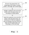
- Fig. 1 shows a flow chart of an embodiment of the inventive method for interconnecting photovoltaic cells in order to form a photovoltaic cells assembly.
- a first photovoltaic cell comprising a first surface, a second surface, a first edge, and a second edge are provided.
- a conductive wire is arranged on the first surface of the first photovoltaic cell according to a certain pattern.
- the conductive wire is attached to the first surface of the first photovoltaic cell with the aid of a first non-conductive yarn by stitching in the area of the first edge of the first photovoltaic cell according to a first stitch type.
- said step 100 can also be a part of the possible preliminary steps as already described above.
- the method comprises the step of additionally attaching the conductive wire to the first surface of the first photovoltaic cell with the aid of a second non-conductive yarn by stitching in the area of the second edge of the first photovoltaic cell according to a second stitch type.
- stitching according to the second stitch type is configured to pull a loop being fed through a hole in the first photovoltaic cell with the aid of the second non-conductive yarn to an edge, preferably the second edge, of the first photovoltaic cell especially along the second surface of the first photovoltaic cell.
- the second stitch type may especially comprise or be an ISO #501 stitch or an over-edge stitch or an overlock stitch or an over-edge chainstitch, preferably a one-thread over-edge chainstitch.
- the first photovoltaic cell may especially comprise or be a thin-film cell such as a copper indium gallium selenide (CIGS) cell.
- said second stitch type can additionally or alternatively comprise or be an ISO #101 stitch or a chainstitch, in particular for the embodiments with cell edge insulation by a transparent insulating foil (which will be described below).
- a transparent insulating foil which will be described below.
- first edge and the second edge may especially be parallel or approximately parallel with respect to each other.
- the conductive wire may especially comprise at least one of copper, nickel, steel, especially stainless steel, aluminum, carbon fiber, or any combination thereof.
- the certain pattern may especially comprise at least one of a zig-zag pattern, a sine-shaped pattern, a pattern being similar to a sine shape, or any combination thereof.
- the first non-conductive yarn may especially comprise polyolefin and/or nylon.
- the second non-conductive yarn may especially comprise polyolefin and/or nylon.
- a swinging arm or beam is used.
- a respective machine stitching presser foot and a corresponding needle may preferably be used.
- the conductive wire may be arranged in such a manner that at least a part, preferably a wire loop or a wire loop pattern, of the conductive wire extends the first surface (preferably beyond an edge, more preferably beyond the second edge) of the first photovoltaic cell especially in the area of the second edge of the first photovoltaic cell.
- the first stitch type comprises or is an ISO #101 stitch or a chainstitch.
- the method may especially comprise the step of cutting the conductive wire if the certain pattern covers the first surface of the first photovoltaic cell according to a predefined manner.
- the method may especially comprise the steps of providing a second photovoltaic cell comprising a first surface, a second surface, a first edge, and a second edge, and aligning the second photovoltaic cell and the first photovoltaic cell especially on the basis of the second edge of the first photovoltaic cell and the first edge of the second photovoltaic cell.
- a second photovoltaic cell is preferably aligned in such a manner that a surface of the second photovoltaic cell covers the part, especially the wire loop or the wire loop pattern, of the conductive wire extending the first surface (preferably beyond an edge, more preferably beyond the second edge) of the first photovoltaic cell.
- the method comprises the step of repeating at least a part of the method steps described above with respect to at least one further photovoltaic cell.
- a wire loop or a wire loop pattern of the conductive wire extending the first surface (preferably beyond an edge, more preferably beyond the second edge) of the first photovoltaic cell may preferably simultaneously be attached to a second surface of a second photovoltaic cell through attaching a conductive wire, preferably a second conductive wire, to a first surface of the second photovoltaic cell with the aid of the first non-conductive yarn by stitching in the area of the first edge of the second photovoltaic cell according to the first stitch type.
- the first non-conductive yarn may be another one than for the first photovoltaic cell.
- the method may especially comprise the step of encapsulating the photovoltaic cells assembly with the aid of an encapsulating material, preferably a thermoplastic material, more preferably a thermoplastic non-reactive material, most preferably a thermoplastic non-reactive polyolefin material.
- an encapsulating material preferably a thermoplastic material, more preferably a thermoplastic non-reactive material, most preferably a thermoplastic non-reactive polyolefin material.
- the melting point of the encapsulating material is below 180 degrees Celsius, preferably between 130 and 150 degrees Celsius.
- the melting point of the first non-conductive yarn may preferably be in the same range as or equal to the melting point of the encapsulating material.
- the melting point of the second non-conductive yarn may preferably be in the same range as or equal to the melting point of the encapsulating material.
- a cell 20, preferably a CIGS cell, is provided or placed, respectively.
- the cell 20 comprises a first edge 21a, exemplarily a bottom edge, a second edge 21b, exemplarily a top edge, a third edge 21c, exemplarily a right edge, a fourth edge 21d, exemplarily a left edge, a first surface 22a, exemplarily a front surface, and a second surface 22b, exemplarily a back surface, which cannot be seen due to the two-dimensional illustration of Fig. 2A .
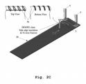
- a swinging beam 1 (preferably working and/or mounted together with two sewing presser feet 3, 4) aligns and guides a conductive Ni-wire 2 with a zigzag pattern on the front surface 22a of the cell 20 or the CIGS cell, respectively.
- the Ni-wire 2 is attached with a polymer yarn 5a (non-conductive, preferably thermoplastic and/or optically transparent and/or with a similar refractive index as module encapsulant material used for the respective embedding process and/or with a similar or higher melting point temperature) to the CIGS cell surface using a stitch ISO #101 class ("chainstitch").
- the stitch is applied using the machine stitching presser foot 3 and a corresponding needle.
- the needle pierces a hole through the CIGS cell 20 and simultaneously feeds the non-conductive yarn 5a through the hole.
- a yarn loop is left behind, which is pulled along the backside surface 22b of the CIGS cell 20 to the area where the needle will feed through a subsequent loop through the CIGS cell 20 (and yarn loop) .
- holes through the cells preferably at the first edge and at the second edge
- Such holes can be made simultaneously with the stitching, for example, by using 2 needles: a first needle to punch a hole, immediately followed by a second needle to do the stitching as already mentioned above.
- the holes can be made beforehand, for example, by punching or by etching.
- This stitch especially is a stitch ISO # 101 class; it is formed by one needle thread (yarn) passing through the CIGS cell 20 and interlooping with itself on the underside of the seam. Meanwhile, the swinging beam 1 progresses along the cell 20 from right (right edge 21c) to left (left edge 21), together with both presser feet 3, 4 and corresponding needles (or alternatively, vice-versa).
- the arm 1 swings to the top edge 21b of the CIGS cell 20. It is attached by a polymer yarn 5b to the CIGS cell 20 using a stitch ISO # 501 class ("1-thread Overedge chainstitch") as illustrated by Fig. 2C .
- This stitch has the feature to pull the loop that is fed through a hole in the CIGS cell 20, to the side edge (especially the second edge 21b) of the cell 20 along the underside surface 22b of the cell 20. It is there pulled up along the edge 21b.
- the non-conductive polymer yarn 5b is now wrapped around the edge 21b of the CIGS cell 20, and simultaneously it is attaching the Ni-wire 2 to the front surface 22a of the CIGS cell 20.
- the ISO #501 class "over edge” or “overlock” stitch type is formed with one needle and 1 looper thread with this thread passing round the edge of the CIGS strip being sewn.
- the swinging arm or beam 1 extends outside the surface area 22a especially beyond the second edge 21b of the CIGS cell 20, before returning to the top side of the cell. This results in a Ni-wire loop that is extending beyond the second edge 21b of the CIGS cell 20. As the wire 2 crosses the path of the top ISO # 501 class stitch again, the wire is attached again to the CIGS cell surface.
- the Ni-wire 2 crosses the bottom edge ISO # 101 class stitch again and is attached to the CIGS cell surface 22a.
- the zigzag trajectory of the Ni wire 2 is secured on four places on the CIGS cell 20 (two at the top edge 21b, two at the bottom edge 21a) surface per single zigzag cycle of the swinging beam/arm 1.
- This sequence of sewing and zigzag arm swinging is repeated along the full length of the first CIGS cell 20, from the third edge 21c to the fourth edge 21d, as shown in Fig. 2D .
- the wire 2 or the yarns 5a, 5b, respectively, are especially cut.
- a new CIGS cell strip 30 or a second cell, respectively, is aligned and placed on the Ni-wire part 2 that is extending beyond the top edge 21b of the first CIGS cell 20.
- said second cell 30 comprises edges and surfaces being analogously denoted with reference signs 31a-31d, 32a, and 32b with respect to the first cell 20.
- the top edge 21b of the first cell 20 that is wrapped with the polymer thread/yarn 5b is separated from the second cell bottom edge 31a (yarn 5b especially acts as a spacer, stitch ISO # 501 class); this advantageously avoids side contacts causing shunts and/or unwanted electrical contacts between both cell strips 20 and 30.
- the stitching sequence of the first step is repeated on the second cell 30 according to Fig. 2F .
- the path of the stitch ISO #101 class at the bottom edge 31a of the second cell strip 30 is also crossing the Ni wire 2 extending/protruding from the first cell 20 underneath the second cell 30, this Ni-wire 2 is, simultaneously with the fixing of the second Ni-wire 2' on the front surface 32a of the second CIGS cell strip 30, also attached to the backside surface 32b of the second CIGS cell strip 30.
- an electrical interconnection is especially created between the top transparent layer on the surface of the first CIGS cell strip 20 and the underside metal surface of the second CIGS cell strip 30. Simultaneously, both cell strips 20, 30 are physically attached to each other to create a cell string.
- Fig. 2G shows four CIGS strips 20, 30, 40, 50 being connected.
- four pieces of wire 2, 2', 2'', 2''' have been used. This analogously applies with respect to the yarn (5a, 5a', 5a", 5a′′′) for the corresponding bottom edge and the yarn (5b, 5b', 5b", 5b′′′) for the corresponding top edge.
- integration of the CIGS cell strings in a photovoltaic module especially depends on the final application.
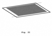
- a possible example of a short process is described to create a module consisting of a transparent front sheet and a back sheet as illustrated by Fig. 2H .
- Fig. 2H a possible example of a short process is described to create a module consisting of a transparent front sheet and a back sheet as illustrated by Fig. 2H .
- other module configurations of integration of CIGS cell strings are possible.
- a glass- or alternative transparent substrate carrier 9 (rigid or flexible) is used to align an encapsulant sheet 8 on.
- the encapsulant sheet may comprise or consist of a non-reactive, preferably thermoplastic, encapsulant material.
- the encapsulant sheet may comprise a single layer or it may be a multi-layer sheet.
- the encapsulant sheet may be a non-reinforced encapsulant sheet or it may preferably be a reinforced encapsulant sheet comprising a glass fibre filling.
- the encapsulant may be consisting of thermoplastic non-reactive polyolefin material compatible with CIGS cell technology, or alternatively an encapsulant should be used that is compatible with CIGS cell technology.
- Strings of interconnected CIGS cells are aligned along one another on the encapsulant sheet 8, and interconnected (via e.g. welding, soldering, conductive adhesives etc.) with bussing ribbons. Suitable terminal ribbons are foreseen at the beginning and end of the CIGS series interconnected cells/strings.
- a second (glass-fibre reinforced) encapsulant sheet 7 may be applied on the CIGS cell string area, and the stack may be covered with a back substrate 6 (for instance, back sheet, glass or the like).
- the module layer stack may be heated to a temperature (for instance, 155-165 degrees Celsius) that is above the melting temperature of the encapsulant material (melting point of 130-150 degrees Celsius) to allow full embedding of the CIGS strings, and to avoid any cavities (but below 180°C to avoid deterioration of the CIGS layers).
- a temperature for instance, 155-165 degrees Celsius
- the melting temperature of the encapsulant material melting point of 130-150 degrees Celsius
- thermoplastic yarn material will melt as melting temperature is in the same range as the melting temperature of the encapsulant.
- the corresponding refractive index may especially be similar to the encapsulant material, improving aesthetical appearance (no yarns visible after lamination).
- FIG. 3A a first exemplary snapshot with respect to the formation of a photovoltaic cells assembly in the context of a further exemplary embodiment of the inventive method is shown.
- this embodiment further comprises a placement of a non-conductive optically transparent foil 23 with one to a few millimeters, preferably 3 millimeters, overlap over the second edge, preferably the top, of the cell 20, exemplarily a CIGS strip.
- the transparent foil is preferably made from or comprises a thermo-plastic material such as a polyolefin material or a thermoset material.
- the transparent foil may be a multilayer foil, such as for example a foil comprising an optically transparent polyurethane layer and a thermoset layer or a thermoplastic layer such as a polyolefin layer or an acrylic layer. By slightly heating this material (for instance, 60 to 120 degrees Celsius, for example 70 to 110 degrees Celsius) it will become sticky and stay fixed onto the CIGS strip.
- the pieces or cell strips can also be up to 4 a 5 cm x 50cm (or other width, for instance, 30 cm).
- a piece of 4 a 5 x 30cm would match with the current of a half silicon cell (i.e., 5 A). This would allow to use conventional half-cell silicon invertors for modules made out of these CIGS cells.
- a swinging beam such as the above-mentioned one 1 (especially working/mounted together with one sewing presser feet such as the above-mentioned one 3) aligns and guides a conductive Ni-wire such as wire 2 with a zigzag pattern on the surface of the CIGS cell such as the surface 22a.
- the Ni-wire 2 When the beam swings to the bottom side of the cell, the Ni-wire 2 is attached with a polymer yarn 5a (non-conductive, preferably thermoplastic, optically transparent, similar refractive index as module encapsulant material used for embedding process, and with a similar or higher melting point temperature) to the CIGS cell surface especially using a stitch ISO #101 class ("chainstitch”) .
- a polymer yarn 5a non-conductive, preferably thermoplastic, optically transparent, similar refractive index as module encapsulant material used for embedding process, and with a similar or higher melting point temperature
- the stitch is applied using a machine stitching presser foot and a corresponding needle.
- the needle pierces a hole through the CIGS cell 20 and simultaneously feeds the non-conductive yarn 5a through the hole.
- a yarn loop is left behind, which is pulled along the backside surface of the CIGS cell 20 to the area where the needle will feed through a subsequent loop through the CIGS cell 20 (and yarn loop).
- This stitch especially is a stitch ISO # 101 class; it is formed by one needle thread (yarn) 5a passing through the CIGS cell 20 and interlooping with itself on the underside of the seam. Meanwhile, the swinging beam progresses along the cell 20 from right to left (on the drawing) . As the Ni-wire 2 is now fixed (attached) to the front side of the cell 20, the arm swings to the top side of the CIGS cell 20 over the non-conductive transparent foil 23. Because this foil is sticky, the Ni-wire 2 will stick where it is placed onto the non-conductive transparent foil 23. Eventually a slightly pressing roller or bar could fix the Ni-wire 2 tighter onto the non-conductive transparent sheet 23.
- the swinging arm or beam extends outside the surface area of the CIGS cell 20, before returning to the top side of the cell 20. This results in a Ni-wire loop that is extending out of the CIGS cell 20. Continuing its trajectory to the bottom side of the CIGS cell 20, the Ni-wire 2 crosses the bottom side ISO # 101 class stitch again and is attached to the CIGS cell surface.
- the zigzag trajectory of the Ni-wire 2 is especially secured on the sticky part of the transparent foil 23 (at the top side of the CIGS cell 20) and at two places at the bottom side by the stitch per single zigzag cycle of the swinging beam/arm.
- This sequence of sewing and zigzag arm swinging is repeated along the full length of the first CIGS cell 20. Once reaching the end, the wires 2 (and yarns 5a) are cut.
- a new CIGS cell strip such as the above-mentioned cells 30, 40, 50 may be aligned and placed on the Ni-wire part that is extending beyond the top side of the first CIGS cell 20.
- the top side border of the first cell 20 is isolated from the second cell bottom side border by the non-conductive transparent foil 23. This avoids side contacts causing shunts or unwanted electrical contacts between both cell strips.
- the above-mentioned stitching sequence may be repeated on the second cell.
- this Ni-wire is, simultaneously with the fixing of the second Ni-wire on the top surface of the second CIGS cell strip, attached to the backside surface of the second CIGS cell strip.
- an electrical interconnection is created between the top transparent layer on the surface of the first CIGS cell strip 20 and the underside metal surface of the second CIGS cell strip.
- both cell strips are physically attached to each other to create a cell string. It also simultaneously will fix the non-conductive foil 23 to the backside of the CIGS cell.
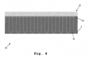
- FIG. 4 an exemplary snapshot with respect to the formation of a photovoltaic cells assembly in the context of a further exemplary embodiment of the inventive method is shown.
- this embodiment further comprises a placement of a non-conductive optically transparent foil 23 with one to a few millimeters, preferably three millimeters, overlap over the top of the CIGS strip 20.
- the transparent foil 23 preferably comprises a thermoplastic material and could be a polyolefin material. By slightly heating this material (for instance, 60 to 120 degrees Celsius, for example 70 to 110 degrees Celsius) it will become sticky and stay fixed onto the CIGS strip 20.
- a swinging beam such as the above-mentioned one 1 (especially working and/or mounted together with two sewing presser feet such as the above-mentioned ones 3 and 4) aligns and guides a conductive Ni-wire 2 with a zigzag pattern on the surface of the CIGS cell.
- the Ni-wire 2 When the beam swings to the bottom side of the cell 20 the Ni-wire 2 is attached with a polymer yarn 5a, 5a' (non-conductive, preferably thermoplastic, optically transparent, similar refractive index as module encapsulant material used for embedding process, and with a similar or higher melting point temperature) to the CIGS cell surface using a stitch ISO #101 class ("chainstitch").
- a polymer yarn 5a, 5a' non-conductive, preferably thermoplastic, optically transparent, similar refractive index as module encapsulant material used for embedding process, and with a similar or higher melting point temperature
- the wire 2 is not only attached to the first edge or the bottom edge, respectively, of the cell 20 with the aid of the yarn 5a, but also to the second edge or the top edge, respectively, of the cell 20 with the aid of the yarn 5a' preferably by using the same stitch type.
- the stitch is applied using the respective machine stitching presser foot and a corresponding needle.
- the needle pierces a hole through the CIGS cell 20 and simultaneously feeds the non-conductive yarn 5a, 5a' through the hole.
- a yarn loop is left behind, which is pulled along the backside surface of the CIGS cell 20 to the area where the needle will feed through a subsequent loop through the CIGS cell 20 (and yarn loop).
- This stitch especially is a stitch ISO # 101 class; it is formed by one needle thread (yarn 5a or 5a', respectively) passing through the CIGS cell 20 and interlooping with itself on the underside of the seam. Meanwhile, the swinging beam progresses along the cell 20 from right to left (on the drawing), together with both presser feet and corresponding needles (or alternatively, vice-versa).
- the arm swings to the top side of the CIGS cell 20.
- it is attached by the polymer yarn 5a' using a stitch ISO #101 class ("chainstitch"). This will stitch the non-conductive transparent foil 23 and the Ni-wire 2 at the same time together.
- the Ni-wire 2 will be on top of this non-conductive transparent foil 23.
- the swinging arm or beam extends outside the surface area of the CIGS cell 20, before returning to the top side of the cell 20. This results in a Ni-wire loop that is beyond the second edge of the CIGS cell 20 and will lay up onto the non-conductive transparent foil 23. As the wire 2 crosses the path of the top ISO # 101 class stitch again, the wire 2 is attached again to the transparent foil 23.
- the Ni-wire 2 crosses the bottom side ISO # 101 class stitch again and is attached to the CIGS cell surface.
- the zigzag trajectory of the Ni-wire 2 is especially secured on four places on the CIGS cell 20 (two at the top side, two at the bottom side) surface per single zigzag cycle of the swinging beam/arm.
- the non-conductive transparent foil 23 is especially stitched between the Ni-wire 2 and the CIGS cell 20. This sequence of sewing and zigzag arm swinging is repeated along the full length of the first CIGS cell 20. Once reaching the end, the wires 2 and/or yarns 5a, 5a' are cut.
- a new CIGS cell strip may be aligned and placed on the Ni-wire part that is extending beyond the top side of the first CIGS cell 20.
- the top side border of the first cell 20 is isolated from the second cell bottom side border by the non-conductive transparent foil 23; this avoids side contacts causing shunts or unwanted electrical contacts between both cell strips.
- the stitching sequence of the above-mentioned step is especially repeated on the second cell.
- this Ni-wire is, simultaneously with the fixing of the second Ni-wire on the top surface of the second CIGS cell strip, attached to the backside surface of the second CIGS cell strip.
- an electrical interconnection is created between the top transparent layer on the surface of the first CIGS cell strip 20 and the underside metal surface of the second CIGS cell strip.
- both cell strips are physically attached to each other to create a cell string.
- the pattern of the conductive wire can be different for different connected cells.
- a different conductive wire pattern may preferably be used for different cell strips within a string. For instance, this may especially be done for creating a visual effect and/or for aesthetical reasons.
Landscapes
- Photovoltaic Devices (AREA)
- Life Sciences & Earth Sciences (AREA)
- Engineering & Computer Science (AREA)
- Sustainable Development (AREA)
- Sustainable Energy (AREA)
Claims (15)
- Ein Verfahren zum Verbinden von photovoltaischen Zellen (20, 30, 40, 50), um eine photovoltaische Zellenanordnung zu bilden, wobei das Verfahren folgende Schritte aufweist:Bereitstellen einer ersten photovoltaischen Zelle (20) mit einer ersten Oberfläche (22a), einer zweiten Oberfläche (22b), einer ersten Kante (21a) und einer zweiten Kante (21b),Anordnen eines elektrisch leitenden Drahts (2) auf der ersten Oberfläche (22a) der ersten photovoltaischen Zelle (20) nach einem bestimmten Muster, sowieBefestigen des elektrisch leitenden Drahts (2) an der ersten Oberfläche (22a) der ersten photovoltaischen Zelle (20) mithilfe eines ersten elektrisch nichtleitenden Fadens (5a) durch Annähen in einem Bereich der ersten Kante (21a) der ersten photovoltaischen Zelle (20) gemäß einem ersten Stichtyp.
- Das Verfahren nach Anspruch 1,
wobei das Verfahren den Schritt des zusätzlichen Befestigens des elektrisch leitenden Drahts (2) an der ersten Oberfläche (22a) der ersten photovoltaischen Zelle (20) mithilfe eines zweiten elektrisch nichtleitenden Fadens (5b) durch Annähen in einem Bereich der zweiten Kante (21b) der ersten photovoltaischen Zelle (20) gemäß einem zweiten Stichtyp. - Das Verfahren nach Anspruch 2,wobei das Annähen gemäß dem zweiten Stichtyp so ausgeführt ist, dass eine Schlaufe, die durch ein Loch in der ersten photovoltaischen Zelle (20) geführt wird, mithilfe des zweiten elektrisch nichtleitenden Fadens (5b) über eine Kante, vorzugsweise die zweite Kante (21b), der ersten photovoltaischen Zelle (20) insbesondere entlang der zweiten Oberfläche (22b) der ersten photovoltaischen Zelle (20) gezogen wird, und/oderwobei der zweite Stichtyp einen ISO #501 Stich oder einen Überwendlich-Stich oder einen Overlock-Stich oder einen Überwendlich-Kettenstich, vorzugsweise einen einfädigen Überwendlich-Kettenstich, aufweist oder bildet.
- Das Verfahren nach Anspruch 2 oder 3,wobei die erste photovoltaische Zelle eine Dünnfilmzelle, vorzugsweise eine Kupfer-Indium-Gallium-Selenid-Zelle oder eine Kupfer-Indium-Selenid-Zelle oder eine Kadmium-Tellurid-Zelle oder eine Perowskit-Zelle oder eine amorphe Siliziumzelle aufweist oder bildet, und/oder wobei die erste Kante (21a) und die zweite Kante (21b) zueinander parallel oder annähernd parallel sind, und/oderwobei der elektrisch leitende Draht (2) mindestens eines der folgenden aufweist: Kupfer, Nickel, Stahl, insbesondere rostfreien Stahl, Aluminium, Kohlefaser oder eine beliebige Kombination aus diesen, und/oderwobei das bestimmte Muster mindestens eines der folgenden aufweist: ein Zickzack-Muster, ein sinusförmiges Muster, ein sinusformähnliches Muster oder eine beliebige Kombination aus diesen, und/oderwobei der erste elektrisch nichtleitende Faden (5a) mindestens eines der folgenden aufweist: Polyolefin, Nylon oder die Kombination aus diesen, und/oderwobei im Falle von Anspruch 2 der zweite elektrisch nichtleitende Faden (5b) mindestens eines der folgenden aufweist: Polyolefin, Nylon oder die Kombination aus diesen.
- Das Verfahren nach einem der Ansprüche 1 bis 4,wobei zur Anordnung des elektrisch leitenden Drahts (2) ein Schwenkarm oder -balken (1) verwendet wird, und/oderwobei zum Nähen ein jeweiliges Maschinennähfüßchen (3, 4) und eine entsprechende Nadel verwendet werden.
- Das Verfahren nach einem der Ansprüche 1 bis 5,
wobei der elektrisch leitende Draht (2) derart angeordnet wird, dass sich mindestens ein Teil, vorzugsweise eine Drahtschlaufe oder ein Drahtschlaufenmuster, des elektrisch leitenden Drahts (2) über die erste Oberfläche (22a) der ersten photovoltaischen Zelle (20) insbesondere im Bereich der zweiten Kante (21b) der ersten photovoltaischen Zelle (20) erstreckt. - Das Verfahren nach einem der Ansprüche 1 bis 5,wobei das Nähen gemäß dem ersten Stichtyp derart ausgeführt wird, dass der erste elektrisch nichtleitende Faden (5a) durch die erste photovoltaische Zelle (20) verläuft und/oder sich selbst auf der zweiten Oberfläche (22b) der ersten photovoltaischen Zelle (20) umschlingt, und/oderwobei der erste Stichtyp einen ISO #101 Stich oder einen Kettenstich aufweist oder bildet.
- Das Verfahren nach einem der Ansprüche 1 bis 7,wobei das Verfahren den Schritt des Schneidens des elektrisch leitenden Drahts (2) aufweist, wenn das bestimmte Muster die erste Oberfläche (22a) der ersten photovoltaischen Zelle (20) in einer vorgegebenen Weise bedeckt, und/oderwobei das Verfahren den Schritt des Schneidens des ersten elektrisch nichtleitenden Fadens (5a) aufweist, wenn das bestimmte Muster die erste Oberfläche (22a) der ersten photovoltaischen Zelle (20) in einer vorgegebenen Weise bedeckt, und/oderwobei, im Falle von einem der Ansprüche 2 bis 7, das Verfahren den Schritt des Schneidens des zweiten elektrisch nichtleitenden Fadens (5b) aufweist, wenn das bestimmte Muster die erste Oberfläche (22a) der ersten photovoltaischen Zelle (20) in einer vorgegebenen Weise bedeckt.
- Das Verfahren nach einem der Ansprüche 1 bis 8,wobei das Verfahren die folgenden Schritte aufweist:Bereitstellen einer zweiten photovoltaischen Zelle (30) mit einer ersten Oberfläche (32a), einer zweiten Oberfläche (32b), einer ersten Kante (31a) und einer zweiten Kante (31b), sowieAusrichten der zweiten photovoltaischen Zelle (30) und der ersten photovoltaischen Zelle (20) insbesondere auf der Basis der zweiten Kante (21b) der ersten photovoltaischen Zelle (20) und der ersten Kante (31a) der zweiten photovoltaischen Zelle (30),wobei die zweite photovoltaische Zelle (30) vorzugsweise derart ausgerichtet wird, dass eine Oberfläche der zweiten photovoltaischen Zelle den Teil, insbesondere die Drahtschlaufe oder das Drahtschlaufenmuster, des elektrisch leitenden Drahts (2) bedeckt, der sich über die erste Oberfläche (22a) der ersten photovoltaischen Zelle (20) erstreckt.
- Das Verfahren nach einem der Ansprüche 1 bis 9,
wobei das Verfahren den Schritt des Wiederholens mindestens eines Teils der Verfahrensschritte nach einem der Ansprüche 1 bis 9 in Bezug auf mindestens eine weitere photovoltaische Zelle (30, 40, 50) aufweist. - Das Verfahren nach Anspruch 10,
wobei eine Drahtschlaufe oder ein Drahtschlaufenmuster des elektrisch leitenden Drahts (2), die/das sich über die erste Oberfläche (22a) der ersten photovoltaischen Zelle (20) erstreckt, vorzugsweise gleichzeitig an einer zweiten Oberfläche (32b) der zweiten photovoltaischen Zelle (30) durch Befestigen eines elektrisch leitenden Drahts, vorzugsweise eines zweiten elektrisch leitenden Drahts (2'), an einer ersten Oberfläche (32a) der zweiten photovoltaischen Zelle (30) mithilfe des ersten elektrisch nichtleitenden Fadens (5a') durch Annähen in dem Bereich der ersten Kante der zweiten photovoltaischen Zelle gemäß dem ersten Stichtyp befestigt wird. - Das Verfahren nach einem der Ansprüche 1 bis 11,
wobei das Verfahren den Schritt des Einkapselns der photovoltaischen Zellenanordnung mithilfe eines Einkapselungsmaterials (7, 8), vorzugsweise eines thermoplastischen Materials, weiter bevorzugt eines thermoplastischen nicht-reaktiven Materials, höchst bevorzugt eines thermoplastischen nicht-reaktiven Polyolefinmaterials, aufweist. - Das Verfahren nach Anspruch 12,
wobei der Schmelzpunkt des Einkapselungsmaterials (7, 8) unter 180 Grad Celsius, vorzugsweise zwischen 140 und 145 Grad Celsius liegt. - Das Verfahren nach Anspruch 12 oder 13,wobei der Schmelzpunkt des ersten elektrisch nichtleitenden Fadens (5a, 5a', 5a", 5a‴) in demselben Bereich liegt wie der oder gleich dem Schmelzpunkt des Einkapselungsmaterials (7, 8) ist, und/oderwobei der Schmelzpunkt des zweiten elektrisch nichtleitenden Fadens (5b, 5b', 5b", 5b‴) in demselben Bereich liegt wie der oder gleich dem Schmelzpunkt des Einkapselungsmaterials (7, 8) ist.
- Eine photovoltaische Zellenanordnung, die durch die Schritte eines Verfahrens nach einem der Ansprüche 1 bis 14 herstellbar ist.
Priority Applications (3)
| Application Number | Priority Date | Filing Date | Title |
|---|---|---|---|
| EP20187110.0A EP3944342B1 (de) | 2020-07-22 | 2020-07-22 | Verfahren zum verbinden von photovoltaischen zellen und dadurch herstellbare photovoltaische zellenanordnung |
| PCT/EP2021/068149 WO2022017756A1 (en) | 2020-07-22 | 2021-07-01 | Method for interconnecting photovoltaic cells and photovoltaic cells assembly being producible thereby |
| US18/006,317 US12419132B2 (en) | 2020-07-22 | 2021-07-01 | Method for interconnecting photovoltaic cells and photovoltaic cell assembly |
Applications Claiming Priority (1)
| Application Number | Priority Date | Filing Date | Title |
|---|---|---|---|
| EP20187110.0A EP3944342B1 (de) | 2020-07-22 | 2020-07-22 | Verfahren zum verbinden von photovoltaischen zellen und dadurch herstellbare photovoltaische zellenanordnung |
Publications (2)
| Publication Number | Publication Date |
|---|---|
| EP3944342A1 EP3944342A1 (de) | 2022-01-26 |
| EP3944342B1 true EP3944342B1 (de) | 2023-11-01 |
Family
ID=71741656
Family Applications (1)
| Application Number | Title | Priority Date | Filing Date |
|---|---|---|---|
| EP20187110.0A Active EP3944342B1 (de) | 2020-07-22 | 2020-07-22 | Verfahren zum verbinden von photovoltaischen zellen und dadurch herstellbare photovoltaische zellenanordnung |
Country Status (3)
| Country | Link |
|---|---|
| US (1) | US12419132B2 (de) |
| EP (1) | EP3944342B1 (de) |
| WO (1) | WO2022017756A1 (de) |
Families Citing this family (2)
| Publication number | Priority date | Publication date | Assignee | Title |
|---|---|---|---|---|
| CN114649436B (zh) * | 2022-05-20 | 2022-08-23 | 英利能源发展有限公司 | 一种新型光伏组件及其制备方法 |
| EP4525056B1 (de) * | 2023-09-14 | 2026-04-01 | IMEC vzw | Technisches gewebe für fotovoltaische module |
Family Cites Families (5)
| Publication number | Priority date | Publication date | Assignee | Title |
|---|---|---|---|---|
| US8212139B2 (en) * | 2008-01-18 | 2012-07-03 | Tenksolar, Inc. | Thin-film photovoltaic module |
| DE102009035703B4 (de) | 2009-08-02 | 2014-11-27 | Solarion Ag | Verfahren zur Herstellung von Verbünden flexibler Dünnschichtsolarzellen |
| HUE051279T2 (hu) * | 2016-01-06 | 2021-03-01 | Flisom Ag | Hajlékony fényelektromos berendezés |
| EP3410494B1 (de) * | 2017-05-29 | 2019-10-09 | Sefar AG | Photovoltaische zelle und module sowie verfahren zu deren herstellung |
| KR101925505B1 (ko) * | 2018-05-11 | 2019-02-26 | 주식회사 광명전기 | 휴대용 박막 태양전지 패널 및 그의 제조 방법 |
-
2020
- 2020-07-22 EP EP20187110.0A patent/EP3944342B1/de active Active
-
2021
- 2021-07-01 US US18/006,317 patent/US12419132B2/en active Active
- 2021-07-01 WO PCT/EP2021/068149 patent/WO2022017756A1/en not_active Ceased
Also Published As
| Publication number | Publication date |
|---|---|
| US20230299226A1 (en) | 2023-09-21 |
| US12419132B2 (en) | 2025-09-16 |
| EP3944342A1 (de) | 2022-01-26 |
| WO2022017756A1 (en) | 2022-01-27 |
Similar Documents
| Publication | Publication Date | Title |
|---|---|---|
| EP2234181B1 (de) | Herstellungsverfahren für ein Solarmodul | |
| US8709841B2 (en) | Woven mesh substrate with semiconductor elements, and method and device for manufacturing the same | |
| US9385255B2 (en) | Integrated thin film solar cell interconnection | |
| US8697980B2 (en) | Photovoltaic module utilizing an integrated flex circuit and incorporating a bypass diode | |
| US8187906B2 (en) | Method for fabricating composite substances for thin film electro-optical devices | |
| US12419132B2 (en) | Method for interconnecting photovoltaic cells and photovoltaic cell assembly | |
| EP2525415A2 (de) | Solarzellenmodul | |
| CN102694037B (zh) | 连接器电极,太阳电池模块和电连接多个太阳电池的方法 | |
| TW200843129A (en) | Photovoltaic module utilizing a flex circuit for reconfiguration | |
| KR20140105520A (ko) | 확장 금속 메쉬의 롤을 사용하는 자동화된 가요성 태양광 전지 제조 및 상호 연결 | |
| EP3400649B1 (de) | Flexible fotovoltaische vorrichtung | |
| WO2010058360A1 (en) | Textile electronic arrangement | |
| US20110240091A1 (en) | Method for Attaching Flat Electronic Components Onto a Flexible Surface Structure | |
| US20240290906A1 (en) | Method and device for wiring photovoltaic cells | |
| EP2869349B1 (de) | Solarzelle und Solarzellenmodul | |
| CN109560147A (zh) | 太阳能电池板 | |
| JP2006165149A (ja) | 光起電力素子、光起電力素子集合体、光起電力素子モジュール、及び、それらの製造方法 | |
| JP4642662B2 (ja) | 光起電力素子 | |
| Borgers et al. | Multi-wire interconnection technologies weaving the way for back contact and bifacial PV modules | |
| AU2020445474B2 (en) | Solar cell panel and method for manufacturing same | |
| KR102042270B1 (ko) | 태양전지 모듈의 수리 방법과 그에 따른 태양 전지 모듈 | |
| KR102198277B1 (ko) | 태양 전지 및 태양 전지 모듈 | |
| JP5435489B2 (ja) | 有機薄膜太陽電池素子、太陽電池モジュールおよび有機薄膜太陽電池素子の製造方法 | |
| Güldner et al. | Flexible, Polymer Encapsulated Solar Modules–A New Concept for Cu-In-S Solar Devices Produced by the CISCuT Technology | |
| JP2006165148A (ja) | 光起電力素子、光起電力素子集合体、光起電力素子モジュール、及び、それらの製造方法 |
Legal Events
| Date | Code | Title | Description |
|---|---|---|---|
| PUAI | Public reference made under article 153(3) epc to a published international application that has entered the european phase |
Free format text: ORIGINAL CODE: 0009012 |
|
| STAA | Information on the status of an ep patent application or granted ep patent |
Free format text: STATUS: THE APPLICATION HAS BEEN PUBLISHED |
|
| AK | Designated contracting states |
Kind code of ref document: A1 Designated state(s): AL AT BE BG CH CY CZ DE DK EE ES FI FR GB GR HR HU IE IS IT LI LT LU LV MC MK MT NL NO PL PT RO RS SE SI SK SM TR |
|
| STAA | Information on the status of an ep patent application or granted ep patent |
Free format text: STATUS: REQUEST FOR EXAMINATION WAS MADE |
|
| 17P | Request for examination filed |
Effective date: 20220525 |
|
| RBV | Designated contracting states (corrected) |
Designated state(s): AL AT BE BG CH CY CZ DE DK EE ES FI FR GB GR HR HU IE IS IT LI LT LU LV MC MK MT NL NO PL PT RO RS SE SI SK SM TR |
|
| GRAP | Despatch of communication of intention to grant a patent |
Free format text: ORIGINAL CODE: EPIDOSNIGR1 |
|
| STAA | Information on the status of an ep patent application or granted ep patent |
Free format text: STATUS: GRANT OF PATENT IS INTENDED |
|
| INTG | Intention to grant announced |
Effective date: 20230623 |
|
| GRAS | Grant fee paid |
Free format text: ORIGINAL CODE: EPIDOSNIGR3 |
|
| GRAA | (expected) grant |
Free format text: ORIGINAL CODE: 0009210 |
|
| STAA | Information on the status of an ep patent application or granted ep patent |
Free format text: STATUS: THE PATENT HAS BEEN GRANTED |
|
| P01 | Opt-out of the competence of the unified patent court (upc) registered |
Effective date: 20230914 |
|
| AK | Designated contracting states |
Kind code of ref document: B1 Designated state(s): AL AT BE BG CH CY CZ DE DK EE ES FI FR GB GR HR HU IE IS IT LI LT LU LV MC MK MT NL NO PL PT RO RS SE SI SK SM TR |
|
| REG | Reference to a national code |
Ref country code: GB Ref legal event code: FG4D |
|
| REG | Reference to a national code |
Ref country code: CH Ref legal event code: EP |
|
| REG | Reference to a national code |
Ref country code: IE Ref legal event code: FG4D |
|
| REG | Reference to a national code |
Ref country code: DE Ref legal event code: R096 Ref document number: 602020020123 Country of ref document: DE |
|
| REG | Reference to a national code |
Ref country code: LT Ref legal event code: MG9D |
|
| REG | Reference to a national code |
Ref country code: NL Ref legal event code: MP Effective date: 20231101 |
|
| PG25 | Lapsed in a contracting state [announced via postgrant information from national office to epo] |
Ref country code: GR Free format text: LAPSE BECAUSE OF FAILURE TO SUBMIT A TRANSLATION OF THE DESCRIPTION OR TO PAY THE FEE WITHIN THE PRESCRIBED TIME-LIMIT Effective date: 20240202 |
|
| PG25 | Lapsed in a contracting state [announced via postgrant information from national office to epo] |
Ref country code: IS Free format text: LAPSE BECAUSE OF FAILURE TO SUBMIT A TRANSLATION OF THE DESCRIPTION OR TO PAY THE FEE WITHIN THE PRESCRIBED TIME-LIMIT Effective date: 20240301 |
|
| PG25 | Lapsed in a contracting state [announced via postgrant information from national office to epo] |
Ref country code: LT Free format text: LAPSE BECAUSE OF FAILURE TO SUBMIT A TRANSLATION OF THE DESCRIPTION OR TO PAY THE FEE WITHIN THE PRESCRIBED TIME-LIMIT Effective date: 20231101 |
|
| REG | Reference to a national code |
Ref country code: AT Ref legal event code: MK05 Ref document number: 1628237 Country of ref document: AT Kind code of ref document: T Effective date: 20231101 |
|
| PG25 | Lapsed in a contracting state [announced via postgrant information from national office to epo] |
Ref country code: NL Free format text: LAPSE BECAUSE OF FAILURE TO SUBMIT A TRANSLATION OF THE DESCRIPTION OR TO PAY THE FEE WITHIN THE PRESCRIBED TIME-LIMIT Effective date: 20231101 |
|
| PG25 | Lapsed in a contracting state [announced via postgrant information from national office to epo] |
Ref country code: AT Free format text: LAPSE BECAUSE OF FAILURE TO SUBMIT A TRANSLATION OF THE DESCRIPTION OR TO PAY THE FEE WITHIN THE PRESCRIBED TIME-LIMIT Effective date: 20231101 |
|
| PG25 | Lapsed in a contracting state [announced via postgrant information from national office to epo] |
Ref country code: ES Free format text: LAPSE BECAUSE OF FAILURE TO SUBMIT A TRANSLATION OF THE DESCRIPTION OR TO PAY THE FEE WITHIN THE PRESCRIBED TIME-LIMIT Effective date: 20231101 |
|
| PG25 | Lapsed in a contracting state [announced via postgrant information from national office to epo] |
Ref country code: NL Free format text: LAPSE BECAUSE OF FAILURE TO SUBMIT A TRANSLATION OF THE DESCRIPTION OR TO PAY THE FEE WITHIN THE PRESCRIBED TIME-LIMIT Effective date: 20231101 Ref country code: LT Free format text: LAPSE BECAUSE OF FAILURE TO SUBMIT A TRANSLATION OF THE DESCRIPTION OR TO PAY THE FEE WITHIN THE PRESCRIBED TIME-LIMIT Effective date: 20231101 Ref country code: IS Free format text: LAPSE BECAUSE OF FAILURE TO SUBMIT A TRANSLATION OF THE DESCRIPTION OR TO PAY THE FEE WITHIN THE PRESCRIBED TIME-LIMIT Effective date: 20240301 Ref country code: GR Free format text: LAPSE BECAUSE OF FAILURE TO SUBMIT A TRANSLATION OF THE DESCRIPTION OR TO PAY THE FEE WITHIN THE PRESCRIBED TIME-LIMIT Effective date: 20240202 Ref country code: ES Free format text: LAPSE BECAUSE OF FAILURE TO SUBMIT A TRANSLATION OF THE DESCRIPTION OR TO PAY THE FEE WITHIN THE PRESCRIBED TIME-LIMIT Effective date: 20231101 Ref country code: BG Free format text: LAPSE BECAUSE OF FAILURE TO SUBMIT A TRANSLATION OF THE DESCRIPTION OR TO PAY THE FEE WITHIN THE PRESCRIBED TIME-LIMIT Effective date: 20240201 Ref country code: AT Free format text: LAPSE BECAUSE OF FAILURE TO SUBMIT A TRANSLATION OF THE DESCRIPTION OR TO PAY THE FEE WITHIN THE PRESCRIBED TIME-LIMIT Effective date: 20231101 Ref country code: PT Free format text: LAPSE BECAUSE OF FAILURE TO SUBMIT A TRANSLATION OF THE DESCRIPTION OR TO PAY THE FEE WITHIN THE PRESCRIBED TIME-LIMIT Effective date: 20240301 |
|
| PG25 | Lapsed in a contracting state [announced via postgrant information from national office to epo] |
Ref country code: SE Free format text: LAPSE BECAUSE OF FAILURE TO SUBMIT A TRANSLATION OF THE DESCRIPTION OR TO PAY THE FEE WITHIN THE PRESCRIBED TIME-LIMIT Effective date: 20231101 Ref country code: RS Free format text: LAPSE BECAUSE OF FAILURE TO SUBMIT A TRANSLATION OF THE DESCRIPTION OR TO PAY THE FEE WITHIN THE PRESCRIBED TIME-LIMIT Effective date: 20231101 Ref country code: PL Free format text: LAPSE BECAUSE OF FAILURE TO SUBMIT A TRANSLATION OF THE DESCRIPTION OR TO PAY THE FEE WITHIN THE PRESCRIBED TIME-LIMIT Effective date: 20231101 Ref country code: NO Free format text: LAPSE BECAUSE OF FAILURE TO SUBMIT A TRANSLATION OF THE DESCRIPTION OR TO PAY THE FEE WITHIN THE PRESCRIBED TIME-LIMIT Effective date: 20240201 Ref country code: LV Free format text: LAPSE BECAUSE OF FAILURE TO SUBMIT A TRANSLATION OF THE DESCRIPTION OR TO PAY THE FEE WITHIN THE PRESCRIBED TIME-LIMIT Effective date: 20231101 Ref country code: HR Free format text: LAPSE BECAUSE OF FAILURE TO SUBMIT A TRANSLATION OF THE DESCRIPTION OR TO PAY THE FEE WITHIN THE PRESCRIBED TIME-LIMIT Effective date: 20231101 |
|
| PG25 | Lapsed in a contracting state [announced via postgrant information from national office to epo] |
Ref country code: DK Free format text: LAPSE BECAUSE OF FAILURE TO SUBMIT A TRANSLATION OF THE DESCRIPTION OR TO PAY THE FEE WITHIN THE PRESCRIBED TIME-LIMIT Effective date: 20231101 |
|
| PG25 | Lapsed in a contracting state [announced via postgrant information from national office to epo] |
Ref country code: CZ Free format text: LAPSE BECAUSE OF FAILURE TO SUBMIT A TRANSLATION OF THE DESCRIPTION OR TO PAY THE FEE WITHIN THE PRESCRIBED TIME-LIMIT Effective date: 20231101 |
|
| PG25 | Lapsed in a contracting state [announced via postgrant information from national office to epo] |
Ref country code: SK Free format text: LAPSE BECAUSE OF FAILURE TO SUBMIT A TRANSLATION OF THE DESCRIPTION OR TO PAY THE FEE WITHIN THE PRESCRIBED TIME-LIMIT Effective date: 20231101 |
|
| PG25 | Lapsed in a contracting state [announced via postgrant information from national office to epo] |
Ref country code: SM Free format text: LAPSE BECAUSE OF FAILURE TO SUBMIT A TRANSLATION OF THE DESCRIPTION OR TO PAY THE FEE WITHIN THE PRESCRIBED TIME-LIMIT Effective date: 20231101 Ref country code: SK Free format text: LAPSE BECAUSE OF FAILURE TO SUBMIT A TRANSLATION OF THE DESCRIPTION OR TO PAY THE FEE WITHIN THE PRESCRIBED TIME-LIMIT Effective date: 20231101 Ref country code: IT Free format text: LAPSE BECAUSE OF FAILURE TO SUBMIT A TRANSLATION OF THE DESCRIPTION OR TO PAY THE FEE WITHIN THE PRESCRIBED TIME-LIMIT Effective date: 20231101 Ref country code: EE Free format text: LAPSE BECAUSE OF FAILURE TO SUBMIT A TRANSLATION OF THE DESCRIPTION OR TO PAY THE FEE WITHIN THE PRESCRIBED TIME-LIMIT Effective date: 20231101 Ref country code: DK Free format text: LAPSE BECAUSE OF FAILURE TO SUBMIT A TRANSLATION OF THE DESCRIPTION OR TO PAY THE FEE WITHIN THE PRESCRIBED TIME-LIMIT Effective date: 20231101 Ref country code: CZ Free format text: LAPSE BECAUSE OF FAILURE TO SUBMIT A TRANSLATION OF THE DESCRIPTION OR TO PAY THE FEE WITHIN THE PRESCRIBED TIME-LIMIT Effective date: 20231101 |
|
| REG | Reference to a national code |
Ref country code: DE Ref legal event code: R097 Ref document number: 602020020123 Country of ref document: DE |
|
| PLBE | No opposition filed within time limit |
Free format text: ORIGINAL CODE: 0009261 |
|
| STAA | Information on the status of an ep patent application or granted ep patent |
Free format text: STATUS: NO OPPOSITION FILED WITHIN TIME LIMIT |
|
| 26N | No opposition filed |
Effective date: 20240802 |
|
| PG25 | Lapsed in a contracting state [announced via postgrant information from national office to epo] |
Ref country code: SI Free format text: LAPSE BECAUSE OF FAILURE TO SUBMIT A TRANSLATION OF THE DESCRIPTION OR TO PAY THE FEE WITHIN THE PRESCRIBED TIME-LIMIT Effective date: 20231101 |
|
| PG25 | Lapsed in a contracting state [announced via postgrant information from national office to epo] |
Ref country code: SI Free format text: LAPSE BECAUSE OF FAILURE TO SUBMIT A TRANSLATION OF THE DESCRIPTION OR TO PAY THE FEE WITHIN THE PRESCRIBED TIME-LIMIT Effective date: 20231101 |
|
| REG | Reference to a national code |
Ref country code: DE Ref legal event code: R079 Ref document number: 602020020123 Country of ref document: DE Free format text: PREVIOUS MAIN CLASS: H01L0031050000 Ipc: H10F0019900000 |
|
| PG25 | Lapsed in a contracting state [announced via postgrant information from national office to epo] |
Ref country code: MC Free format text: LAPSE BECAUSE OF FAILURE TO SUBMIT A TRANSLATION OF THE DESCRIPTION OR TO PAY THE FEE WITHIN THE PRESCRIBED TIME-LIMIT Effective date: 20231101 |
|
| REG | Reference to a national code |
Ref country code: CH Ref legal event code: PL |
|
| PG25 | Lapsed in a contracting state [announced via postgrant information from national office to epo] |
Ref country code: LU Free format text: LAPSE BECAUSE OF NON-PAYMENT OF DUE FEES Effective date: 20240722 |
|
| GBPC | Gb: european patent ceased through non-payment of renewal fee |
Effective date: 20240722 |
|
| PG25 | Lapsed in a contracting state [announced via postgrant information from national office to epo] |
Ref country code: LU Free format text: LAPSE BECAUSE OF NON-PAYMENT OF DUE FEES Effective date: 20240722 |
|
| PG25 | Lapsed in a contracting state [announced via postgrant information from national office to epo] |
Ref country code: CH Free format text: LAPSE BECAUSE OF NON-PAYMENT OF DUE FEES Effective date: 20240731 Ref country code: BE Free format text: LAPSE BECAUSE OF NON-PAYMENT OF DUE FEES Effective date: 20240731 |
|
| PG25 | Lapsed in a contracting state [announced via postgrant information from national office to epo] |
Ref country code: GB Free format text: LAPSE BECAUSE OF NON-PAYMENT OF DUE FEES Effective date: 20240722 |
|
| REG | Reference to a national code |
Ref country code: BE Ref legal event code: MM Effective date: 20240731 |
|
| PG25 | Lapsed in a contracting state [announced via postgrant information from national office to epo] |
Ref country code: IE Free format text: LAPSE BECAUSE OF NON-PAYMENT OF DUE FEES Effective date: 20240722 |
|
| PG25 | Lapsed in a contracting state [announced via postgrant information from national office to epo] |
Ref country code: FI Free format text: LAPSE BECAUSE OF FAILURE TO SUBMIT A TRANSLATION OF THE DESCRIPTION OR TO PAY THE FEE WITHIN THE PRESCRIBED TIME-LIMIT Effective date: 20231101 |
|
| PGFP | Annual fee paid to national office [announced via postgrant information from national office to epo] |
Ref country code: DE Payment date: 20250620 Year of fee payment: 6 |
|
| PG25 | Lapsed in a contracting state [announced via postgrant information from national office to epo] |
Ref country code: RO Free format text: LAPSE BECAUSE OF FAILURE TO SUBMIT A TRANSLATION OF THE DESCRIPTION OR TO PAY THE FEE WITHIN THE PRESCRIBED TIME-LIMIT Effective date: 20231101 |
|
| PG25 | Lapsed in a contracting state [announced via postgrant information from national office to epo] |
Ref country code: CY Free format text: LAPSE BECAUSE OF FAILURE TO SUBMIT A TRANSLATION OF THE DESCRIPTION OR TO PAY THE FEE WITHIN THE PRESCRIBED TIME-LIMIT; INVALID AB INITIO Effective date: 20200722 |
|
| PG25 | Lapsed in a contracting state [announced via postgrant information from national office to epo] |
Ref country code: HU Free format text: LAPSE BECAUSE OF FAILURE TO SUBMIT A TRANSLATION OF THE DESCRIPTION OR TO PAY THE FEE WITHIN THE PRESCRIBED TIME-LIMIT; INVALID AB INITIO Effective date: 20200722 |
|
| PG25 | Lapsed in a contracting state [announced via postgrant information from national office to epo] |
Ref country code: TR Free format text: LAPSE BECAUSE OF FAILURE TO SUBMIT A TRANSLATION OF THE DESCRIPTION OR TO PAY THE FEE WITHIN THE PRESCRIBED TIME-LIMIT Effective date: 20231101 |
|
| PGFP | Annual fee paid to national office [announced via postgrant information from national office to epo] |
Ref country code: FR Payment date: 20260618 Year of fee payment: 7 |