EP3944301A1 - Semiconductor structure and manufacturing method therefor - Google Patents
Semiconductor structure and manufacturing method therefor Download PDFInfo
- Publication number
- EP3944301A1 EP3944301A1 EP21785747.3A EP21785747A EP3944301A1 EP 3944301 A1 EP3944301 A1 EP 3944301A1 EP 21785747 A EP21785747 A EP 21785747A EP 3944301 A1 EP3944301 A1 EP 3944301A1
- Authority
- EP
- European Patent Office
- Prior art keywords
- patterns
- trenches
- dielectric layer
- semiconductor structure
- manufacturing
- Prior art date
- Legal status (The legal status is an assumption and is not a legal conclusion. Google has not performed a legal analysis and makes no representation as to the accuracy of the status listed.)
- Granted
Links
Images


Classifications
-
- H—ELECTRICITY
- H10—SEMICONDUCTOR DEVICES; ELECTRIC SOLID-STATE DEVICES NOT OTHERWISE PROVIDED FOR
- H10P—GENERIC PROCESSES OR APPARATUS FOR THE MANUFACTURE OR TREATMENT OF DEVICES COVERED BY CLASS H10
- H10P50/00—Etching of wafers, substrates or parts of devices
- H10P50/69—Etching of wafers, substrates or parts of devices using masks for semiconductor materials
- H10P50/691—Etching of wafers, substrates or parts of devices using masks for semiconductor materials for Group V materials or Group III-V materials
- H10P50/693—Etching of wafers, substrates or parts of devices using masks for semiconductor materials for Group V materials or Group III-V materials characterised by their size, orientation, disposition, behaviour or shape, in horizontal or vertical plane
-
- H—ELECTRICITY
- H10—SEMICONDUCTOR DEVICES; ELECTRIC SOLID-STATE DEVICES NOT OTHERWISE PROVIDED FOR
- H10P—GENERIC PROCESSES OR APPARATUS FOR THE MANUFACTURE OR TREATMENT OF DEVICES COVERED BY CLASS H10
- H10P50/00—Etching of wafers, substrates or parts of devices
- H10P50/69—Etching of wafers, substrates or parts of devices using masks for semiconductor materials
- H10P50/691—Etching of wafers, substrates or parts of devices using masks for semiconductor materials for Group V materials or Group III-V materials
- H10P50/693—Etching of wafers, substrates or parts of devices using masks for semiconductor materials for Group V materials or Group III-V materials characterised by their size, orientation, disposition, behaviour or shape, in horizontal or vertical plane
- H10P50/695—Etching of wafers, substrates or parts of devices using masks for semiconductor materials for Group V materials or Group III-V materials characterised by their size, orientation, disposition, behaviour or shape, in horizontal or vertical plane characterised by the process involved to create the mask, e.g. lift-off masks or sidewalls or to modify the mask
-
- H—ELECTRICITY
- H10—SEMICONDUCTOR DEVICES; ELECTRIC SOLID-STATE DEVICES NOT OTHERWISE PROVIDED FOR
- H10W—GENERIC PACKAGES, INTERCONNECTIONS, CONNECTORS OR OTHER CONSTRUCTIONAL DETAILS OF DEVICES COVERED BY CLASS H10
- H10W10/00—Isolation regions in semiconductor bodies between components of integrated devices
- H10W10/01—Manufacture or treatment
- H10W10/011—Manufacture or treatment of isolation regions comprising dielectric materials
- H10W10/014—Manufacture or treatment of isolation regions comprising dielectric materials using trench refilling with dielectric materials, e.g. shallow trench isolations
-
- H—ELECTRICITY
- H10—SEMICONDUCTOR DEVICES; ELECTRIC SOLID-STATE DEVICES NOT OTHERWISE PROVIDED FOR
- H10W—GENERIC PACKAGES, INTERCONNECTIONS, CONNECTORS OR OTHER CONSTRUCTIONAL DETAILS OF DEVICES COVERED BY CLASS H10
- H10W10/00—Isolation regions in semiconductor bodies between components of integrated devices
- H10W10/10—Isolation regions comprising dielectric materials
- H10W10/17—Isolation regions comprising dielectric materials formed using trench refilling with dielectric materials, e.g. shallow trench isolations
-
- H—ELECTRICITY
- H10—SEMICONDUCTOR DEVICES; ELECTRIC SOLID-STATE DEVICES NOT OTHERWISE PROVIDED FOR
- H10B—ELECTRONIC MEMORY DEVICES
- H10B12/00—Dynamic random access memory [DRAM] devices
-
- H—ELECTRICITY
- H10—SEMICONDUCTOR DEVICES; ELECTRIC SOLID-STATE DEVICES NOT OTHERWISE PROVIDED FOR
- H10B—ELECTRONIC MEMORY DEVICES
- H10B12/00—Dynamic random access memory [DRAM] devices
- H10B12/01—Manufacture or treatment
Definitions
- the present application relates to a semiconductor device structure and a method for making the same.
- Dynamic random access memory is a kind of semiconductor memory devices widely used in multiple computer systems.
- the critical dimensions of the dynamic random access memory are getting ever smaller.
- the active areas (AA) are becoming increasingly smaller, setting very high requirements for corresponding semiconductor manufacturing process.
- one of the various embodiments discloses a method for manufacturing a semiconductor device structure, the method includes: providing a substrate which has a plurality of first trenches, in which first patterns are formed between two adjacent ones of the plurality of first trenches; forming a first dielectric layer, in which the first dielectric layer covers at least the sidewall of the first pattern; and segmenting the first pattern to form a second pattern.
- a semiconductor devise structure which includes: a substrate; a plurality of first trenches and a plurality of second trenches both disposed in the substrate; second patterns disposed between the first trenches and the second trenches; a first dielectric layer disposed to cover at least sidewalls of the second patterns adjacent to the first trenches; and a second dielectric layer filling the second trenches.
- Reference numerals in the figures 1 . Substrate; 11. First pattern; 111. Second pattern; 12. First trench; 112. Second trench; 2. First dielectric layer; 3. Patterned mask layer; 31. Opening pattern; 4. The second dielectric layer; and 5. The third dielectric layer.
- the ends of such elongated active area are usually damaged during etching with an existing etching process.
- a one-step etching process is used to dry-etch the substrate to form shallow trenches in the substrate to isolate a number of active regions in the substrate, and then the shallow trenches are filled with an insulating material layer to form shallow trench isolation structures.
- the existing dry etching process to directly etch the substrate to form the active areas, especially as the design dimensions decrease, the ends of such active areas become more and more elongated. Because of high-energy charged particles or groups contained in the etching gas, as the charged particles or groups bombard the substrate to form shallow trenches, they cause damage or destruction to the ends of the active areas, which will have an adverse effect on the performance of the device.
- the present disclosure provides a method for manufacturing a semiconductor structure, which includes:
- the method for preparing the semiconductor structure according to the present disclosure obtain the active areas composed of the second patterns by forming a first dielectric layer as a protective layer on the sidewalls of the first patterns in the substrate, and then segmenting the first patterns to form the second patterns.
- the second patterns constituting the active areas forms from segmenting the first patterns
- the sidewalls of the first patterns are always protected by the first dielectric layer, so the ends of the second patterns (which are the ends of the active areas) are not easily damaged during the segmentation process.
- S1 may include the steps of:
- the substrate 1 can be, but not limited to a silicon substrate, a gallium nitride substrate, a silicon-on-insulator or a silicon carbide substrate, etc.
- the substrate 1 may be a silicon substrate.
- a doped well region by applying an ion implantation process may be formed in the substrate 1, and the doping type of the doped well region may be P-type or N-type.
- each line element of the first patterns 11 may be, but is not limited to, a rectangular wall-shaped structure.
- the plurality of the first patterns 11 are spaced apart, and the first trenches 12 are formed between adjacent first patterns 11.
- the plurality of the first patterns 11 are arranged in parallel at intervals.
- the width d of a first pattern 11 along the horizontal direction of the substrate 1 can be set according to actual needs. It is worth noting that the width d of the first pattern 11 is the lenth, along the horizontal direction of the substrate 1, of the cross section perpendicular to the extension direction of the first pattern 11. Preferably, the width d of the first pattern 11 may be ⁇ 20 nm, and more specifically, the width d of the first pattern 11 may be 20 nm, 15 nm, or 10nm, etc. Within the width range, the technical problem described in the present disclosure is more prominent, and the technical solution described in this embodiment has better economic efficiency and beneficial technical effects.
- the distance L between adjacent first patterns 11 may be set according to actual needs.
- the distance L between the adjacent first patterns 11 may be ⁇ 30 nm, and more specifically, the distance L between the adjacent first patterns 11 may be 30 nm, 25 nm, 20nm, 15nm or 10nm and so on. It should be noted that the distance between the adjacent first patterns 11 refers to the center-to-center distance between the adjacent two first patterns 11.
- a SADP Self-Aligned Double Patterning
- a SAQP Self-Aligned Quadruple Patterning
- S2 may further include the following steps.
- the first dielectric layer 2 is formed on the sidewalls of the first pattern 11 and the bottom surfaces of the first trenches 12; alternatively, the first dielectric layer 2 may also be formed on the sidewalls of the first pattern 11, the bottom surfaces of the first trenches 12, and the top surfaces of the first pattern 11, so that when the second trenches are subsequently formed in an etching process, the first dielectric layer 2 can effectively protect the surfaces of the first pattern 11.
- the thickness of the first dielectric layer 2 can be set according to actual needs. Specifically, the thickness of the first dielectric layer 2 is less than half of the width of a first trench 12. In this process, after the first dielectric layer 2 is formed, there are a gap in the first trenches 12, as shown in FIG. 3 .
- the thickness of the first dielectric layer 2 is in the range of 1nm-5nm. Within this range, the first dielectric layer 2 can not only provide sufficient protection for the first pattern 11, but also leave enough space for subsequent filling of the third dielectric layer.
- a third dielectric layer 5 is formed in the first trenches 12 and fills up the first trenches 12. Specifically, the third dielectric layer 5 fills up the gapsbetween the first dielectric layer 2 in the first trenches 12, as shown in FIG. 5 .
- S22 may include these exemplary steps.
- the third dielectric material layer (not shown) is formed, which fills up the first trenches 12 and covers the first dielectric layer 2 on the top surfaces of the first pattern 11.
- the third dielectric material layer is deposited by a process of, but not limited to, a physical vapor deposition process, a chemical vapor deposition process, an atomic layer deposition process, or a spin coating process;
- the third dielectric material layer which covers the top surfaces of the first patterns 11 is removed, and the retained third dielectric material layer in the first trenches 12 is as the third dielectric layer 5.
- the third dielectric material layer covering the first dielectric layer 2 on the top surfaces of the first patterns 11 is removed by a process such as, but not limited to, the chemical mechanical polishing process.
- the third dielectric material layer is located on the first dielectric layer 2 on the top surfaces of the first patterns 11.
- the third dielectric material layer both on the first dielectric layer 2 on the top surface of the first pattern 11 and in the first trenches 12 has a continuous flat upper surface.
- the method further includes removing the first dielectric layer 2 located at the bottom surfaces of the first trenches 12.
- the first dielectric layer 2 is discontinuous at the bottoms of the first trenches 12 into separated structures, to avoid too many carriers accumulate at the bottoms of the first trenches 12, thereby avoiding leakage current caused by holes or electrons accumulated near the first dielectric layer 2 in the transistor substrate.
- the first dielectric layer 2 at the bottoms of the first trenches 12 can be completely removed or partially removed. In this embodiment, all the first dielectric layer 2 at the bottoms of the first trenches 12 is removed.
- S2 may include the following steps of forming a first dielectric layer 2 in the first trenches 12, which fills up the first trenches 12. Specifically, a first dielectric material layer (not shown) may be formed in the first trenches 12 and the top surfaces of the first pattern 11 firstly, and then the first dielecric material layer on the top surfaces of the first patterns 11 are removed by a process such as, but not limited to, a chemical mechanical polishing process. The first dielectric material layer remaining in the first trenches 12 is the first dielectric layer.
- the first dielectric layer 2 serves as a protective layer for the first patterns 11.
- the first dielectric layer 2 may include, but is not limited to, a silicon dioxide (SiO 2 ) layer, a silicon monoxide (SiO) layer, a silicon nitride (SiN) layer, or a silicon oxynitride (SiON) layer, etc.
- the first dielectric layer 2 can be a silicon dioxide layer.
- the third dielectric layer 5 may include, but is not limited to, a silicon dioxide layer.
- the hardness of the first dielectric layer 2 is greater than the hardness of the third dielectric layer 5, so that the first dielectric layer 2 provides good protection for the first patterns 11.
- the etching rate of the third dielectric layer 5 is greater than the etching rate of the first dielectric layer 2, so as to ensure that when the third dielectric layer 5 is removed, the first dielectric layer 2 on the upper surfaces of the first patterns 11 is hardly removed.
- S3 may include the following steps.
- a plurality of second trenches 112 are formed on each of the first patterns 11 to divide each of the first patterns 11 into a plurality of second patterns 111.
- step S31 may include the following steps.
- a mask layer is formed on the upper surface of the substrate 1.
- a patterning process on the mask layer is performed to obtain a patterned mask layer 3.
- the patterned mask layer 3 includes a plurality of openings 31 penetrating through the mask layer, and the openings 31 define the positions and the shape of the second trenches 112 as shown in FIG. 6 .
- the shape of the openings 31 is a circle, an ellipse or a rectangle, etc.
- the first patterns 11 are etched based on the patterned mask 3 to form the plurality of second trenches 112 on the first patterns 11 to divide each of the first patterns 11 into the plurality of second patterns 112.
- the patterned mask layer 3 is removed, as shown in FIG. 7 .
- the mask layer 3 may include one of or a combination of at least two of an amorphous carbon layer, a silicon oxynitride layer and a silicon oxide layer, but not limited thereto.
- the mask layer may be formed by at least one of the processes of a physical vapor formation process, a chemical a vapor phase formation process, an atomic layer formation process and a spin coating process.
- the mask layer 3 may be patterned by a photolithography process to obtain the pattern mask layer 3.
- the dimension of the openings 31 is larger than the width of each first pattern 11.
- the dimension of the openings 31 may be the size along the width of the first patterns 11, or the maximum size along a horizontal direction of the substrate.
- the width of the first patterns 11 is less than or equal to 20nm
- the size of the second trenches 112 is less than or equal to 15nm
- the thickness of the first dielectric layer 2 ranges from 1nm to 5nm
- the size of the openings 31 is less than 30nm.
- the opening size being larger than the width of the first patterns 11 is beneficial to increase the process window and improves the product yield.
- the size of the second trenches 112 may be the size along the width direction of the first patterns 11, or the maximum size along a horizontal direction of the substrate.
- a dry etching process may be used to pattern the first patterns 11 with the patterned mask layer 3.
- the second trenches 112 segment the first patterns 11 only, but do not cut the first dielectric layer 2 which covers the sidewalls of the first patterns 11.
- the first patterns 11 are etched with an etching process that has an etch selection ratio of greater than 8 between the first patterns 11 and the first dielectric layer 2 to form the second trentches 112, and second patterns 111 are formed between the first trenches 12 and the second trenches 112.
- the first dielectric layer 2 on the sidewalls of the second patterns adjacent to the second trenches 112 is not etched. With the etching process having the high etch selection ratio, only the first patterns 11 are etched and segmented, and the whole first dielectric layer 2 is retained intact, which ensures better end shapes of the second patterns 111, thereby improving the device performance.
- an etching process or a chemical mechanical polishing process may be used to remove the patterned mask layer 3.
- the extending direction of the first patterns 11 is obliquely intersected with the arrangement direction of the second trenches 112 with the shortest adjacent distance in each of the columns.
- the second trenches 112 on a same first pattern 11 are arranged at intervals, and the second trenches 112 on the adjacent first patterns 11 are arranged in a staggered way.
- the second trenches 112 located in adjacent odd-numbered columns of the first pattern 11 are arranged in a staggered way with the second trenches 112 located in the nearby even-numbered columns of the first pattern 11, the second trenches 112 located in the adjacent odd-numbered columns of the first pattern 11 are arranged in one-to-one correspondence, and the second trenches 112 in adjacent even-numbered columns of the first pattern 11 are arranged in a one-to-one correspondence.
- the first patterns are the active areas of the storage device, and the above arrangement is beneficial to maximize the device storage density.
- the depth HI of the first trenches 12 may be greater than or equal to the depth H2 of the second trenches 112.
- the depth HI of the first trenches 12 may be greater than the depth H2 of the second trenches 112.
- the isolation effect is better, and thus the mutual influence between the adjacent active areas is avoid.
- the first trenches 12 can be etched with the above process, and the second trenches 112 can be etched later, that is, different depths in HI of the first trenches 12 and H2 of the second trenches 112 are achieved by twice etching.
- the width D1 of the first trenches 12 is narrower than or equal to the width D2 of the second trenches 112.
- the width D1 of the first trenches 12 is less than the width D2 of the second trenches 112.
- the width of the second trenches 112 refers to the dimension along the extending direction of the first patterns 11.
- the maximum dimension of the second trenches 112 in a horizontal direction of the substrate 1 is less than 15 nm.
- S32 is further included, which includes filling a second dielectric layer 4 in the second trenches 112, as shown in FIG. 8 .
- the second dielectric layer 4 can be formed by a process of, but not limited to, a physical vapor formation process, a chemical vapor formation process, or an atomic layer formation process.
- the material of the second dielectric layer 4 may be the same the material of the first dielectric layer 2, or it can be different from that of the first dielectric layer 2.
- the material of the second dielectric layer 4 and the material of the third dielectric layer 5 may be the same or different.
- the second dielectric layer 4 may include, but not limited to, a silicon oxide layer or a silicon nitride (SiN) layer.
- the viscosity of the second dielectric layer 4 is lower than that of the third dielectric layer 5.
- the first trenches 12 and the second trenches 112 are respectively filled with the third dielectric layer 5 and the second dielectric layer 4 which have different viscosities, ensuring the filling quality and the isolation performance as well.
- the first dielectric layer 2 may also include the step of removing the first dielectric layer 2 from the first trenches 12, and in this case, while filling the second dielectric layer 4 into the second trenches 112, the first trenches 12 are filled with the second dielectric layer 4.
- the first trenches 12 may also include a step of removing the third dielectric layer 5 from the first trenches 12, and in this case, when filling the second dielectric layer 4 into the second trenches 112, the first trenches 12 are filled with the second dielectric layer 4.
- the disclosure is simple in manufacture processes and has a broad prospect for applications in the semiconductor manufacturing field, and it effectively overcomes the shortcomings in the related art and having a high industrial application value.
- the exemplary embodiments of the present disclosure also provide a semiconductor structure.
- the semiconductor structure may be formed by the method described in the above embodiments. Other methods may also be used.
- the semiconductor structure includes: a substrate 1; a number of first trenches 12 and a number of second trenches 112 both located in the substrate 1; second patterns 111 located between the first trenches 12 and the second trenches 112; a first dielectric layer 2, covering at least the sidewalls of the second pattern 111 adjacent to the first trenches 12; and a second dielectric layer 4, filling the second trenches 112.
- the substrate 1 includes, but is not limited to, a silicon substrate, a gallium nitride substrate, a silicon-on-insulator substrate or a silicon carbide substrate, etc.
- the substrate 1 may be a silicon substrate.
- a doped well region formed with an ion implantation process may be formed in the substrate 1, and the dopant type of the doped well region may be either P-type or N-type.
- the depth HI of the first trenches 12 may be greater than or equal to the depth H2 of the second trenches 112. In this embodiment, the depth HI of the first trenches 12 being greater than the depth H2 of the second trenches 112 makes the isolation effect better, so to avoid mutual influence between adjacent active areas.
- the material of the second dielectric layer 4 may be the same as the material of the first dielectric layer 2, or may be different from the material of the first dielectric layer 2.
- the second dielectric layer 4 may include, but is not limited to, a silicon oxide layer or a silicon nitride (SiN) layer.
- the width of the second patterns 111 is less than or equal to 20 nm. It is worth noting that the width of the second patterns 111 is the length, along the horizontal direction of the substrate 1, of the cross section perpendicular to the extension direction of the second patterns 111. Specifically, the width of the second patterns 111 may be 20 nm, 15 nm, or 10 nm, etc. Within the width range, the technical problem described in the present disclosure is more prominent, and the technical solution described in this embodiment will be more economical and more beneficial. The distance between adjacent second patterns 111 can be set according to actual needs.
- the sidewalls of the second pattern 111 adjacent to the second trenches 112 are not covered with the first dielectric layer 2.
- the distance between two adjacent second pattern 111 is ⁇ 30 nm. More specifically, the distance between the adjacent second pattern 111 may be 30 nm, 25 nm, 20 nm, 15 nm, or 10 nm, etc., but in other embodiments, the distance between two adjacent second patterns 111 is not limited to the above-mentioned values. It should be noted that the distance between two adjacent ones of the second patterns 111 mentioned herein refers to the center-to-center distance between two adjacent second patterns 111.
- the maximum dimension of one of the second trenches 112 in a horizontal direction of the substrate 1 is less than 15 nm.
- the semiconductor structure further includes a third dielectric layer 5, and the third dielectric layer 5 fills in the first trenches 12.
- the material of the third dielectric layer 5 is different from the material of the first dielectric layer 2.
- the third dielectric layer 5 may include, but is not limited to, a silicon dioxide layer.
- the material of the second dielectric layer 4 and the material of the third dielectric layer 5 may be the same or different.
- the viscosity of the second dielectric layer 4 is lower than that of the third dielectric layer 5.
- the first trench 12 and the second trench 112 are respectively filled with the third dielectric layer 5 and the second dielectric layer 4 which have different viscosities, thereby ensuring both the filling effect and the isolation performance.
- the width of the first patterns 11 is less than or equal to 20 nm
- the distance between adjacent first patterns 11 is less than or equal to 30 nm
- the size of the second trenches 112 is less than or equal to 15 nm
- the thickness of the first dielectric layer 2 ranges from 1 nm to 5 nm.
- the spin coating process may be used to fill the first trenches 12 and the second trenches 112.
- the second trenches 112 are filled with the second dielectric layer 4 with a low viscosity to obtain a better filling effect, and the first trenches 12 can be filled with a high-viscosity third dielectric layer 5 to obtain a better isolation performance.
- the size of the second trenches 112 may be the size along the width direction of the first patternes 11, or the maximum size along the horizontal direction of the substrate.
- the first dielectric layer 2 is also present between the adjacent second patterns 111 and is integrated with the first dielectric layer 2 on the sidewalls of the second patterns 111.
- the second trenches 112 only segment the first patterns 11, and the first dielectric layer 2 covering the sidewalls of the first patterns 11 is not segmented.
- an etching process with an etch selection ratio greater than 8 between the first patterns 11 and the first dielectric layer 2 the first patterns 11 arevpatterned to form the second trenches 112.
- the second patterns 111 are formed between the first trenches 12 and the second trenches 112 , and the first dielectric layer 2 on the sidewalls of the second patterns 111 adjacent to the second trenches 112 is not segmented by this etching.
- the process with the high etch selection ratio only the first patterns 11 are segmented and the first dielectric layer 2 is retained intact, so the end shape of the resultant second patterns 111 will be better ensured, thereby improving the device performance.
Landscapes
- Engineering & Computer Science (AREA)
- Manufacturing & Machinery (AREA)
- Element Separation (AREA)
Abstract
Description
- This application claims priority to
Chinese Patent Application No. 202010428538.8, filed on May 20, 2020 - The present application relates to a semiconductor device structure and a method for making the same.
- Dynamic random access memory (DRAM) is a kind of semiconductor memory devices widely used in multiple computer systems. With the development of semiconductor integrated circuit device technologies, the critical dimensions of the dynamic random access memory are getting ever smaller. For example, the active areas (AA) are becoming increasingly smaller, setting very high requirements for corresponding semiconductor manufacturing process.
- According to the present disclosure, one of the various embodiments discloses a method for manufacturing a semiconductor device structure, the method includes: providing a substrate which has a plurality of first trenches, in which first patterns are formed between two adjacent ones of the plurality of first trenches; forming a first dielectric layer, in which the first dielectric layer covers at least the sidewall of the first pattern; and segmenting the first pattern to form a second pattern.
- Another embodiment discloses a semiconductor devise structure, which includes: a substrate; a plurality of first trenches and a plurality of second trenches both disposed in the substrate; second patterns disposed between the first trenches and the second trenches; a first dielectric layer disposed to cover at least sidewalls of the second patterns adjacent to the first trenches; and a second dielectric layer filling the second trenches. The details of one or more embodiments of the disclosure are set forth in the following drawings and description. Other features and advantages of the disclosure will become apparent from the description, drawings and claims.
- In order to more clearly illustrate the technical solutions in the embodiments of the present application, the following will briefly introduce the drawings needed in the embodiments. Apparently, the drawings in the following description are only some embodiments of the present application For those of ordinary skill in the art, without creative work, other drawings can be obtained from these drawings.
-
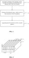
FIG. 1 is a flow chart of the method for preparing the semiconductor structure of the present disclosure; -
FIG. 2 shows a schematic diagram of a perspective view of the substrate having a plurality of first trenches obtained in step S2 according to an embodiment of the present disclosure; -
FIG. 3 shows a schematic diagram of a perspective view of the semiconductor structure obtained in step S21 according to an embodiment of the present disclosure; -
FIG. 4 shows a schematic diagram of a perspective view of the semiconductor structure obtained after removing the first dielectric layer from the bottom of the first trenches according to an embodiment of the present disclosure; -
FIG. 5 shows a schematic diagram of a perspective view of the semiconductor structure obtained in step S22 according to an embodiment of the present disclosure; -
FIG. 6 is a schematic diagram of a perspective view of the semiconductor structure obtained in step S312 according to an embodiment of the present disclosure; -
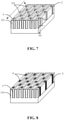
FIG. 7 shows a schematic diagram of a perspective view of the semiconductor structure obtained in step S314 according to an embodiment of the present disclosure; -
FIG. 8 shows a schematic diagram of a perspective view of the semiconductor structure obtained in step S32 according to an embodiment of the present disclosure; -
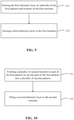
FIG. 9 is a flowchart of an exemplary method of step S2 according to an embodiment of the present disclosure; and -
FIG. 10 is a flowchart of an exemplary method of step according to an embodiment of the present disclosure. - Reference numerals in the
figures: 1 . Substrate; 11. First pattern; 111. Second pattern; 12. First trench; 112. Second trench; 2. First dielectric layer; 3. Patterned mask layer; 31. Opening pattern; 4. The second dielectric layer; and 5. The third dielectric layer. - As the wide of an active area is very narrow, the ends of such elongated active area are usually damaged during etching with an existing etching process.
- In order to better understand the purpose, technical solutions, and technical effects of the present disclosure, the present disclosure will be further explained below in conjunction with the accompanying drawings and embodiments. At the same time, it is stated that the embodiments described below are only used to explain the present disclosure, not to limit the present disclosure.
- Unless otherwise defined, all technical and scientific terms used herein have the same meaning as commonly understood by those skilled in the technical field of the disclosure. The terminology used in the specification of the application herein is only for the purpose of describing specific embodiments, and is not intended to limit the application. The term "and/or" as used herein includes any and all combinations of one or more related listed items.
- In the case of using the "including", "having", and "including" described in this article, unless a clear qualifying term is used, such as "only", "consisting of", etc., another component or process may be added. Unless mentioned to the contrary, terms in the singular form may include the plural form, and it cannot be understood that the number is one.
- In the existing semiconductor process, a one-step etching process is used to dry-etch the substrate to form shallow trenches in the substrate to isolate a number of active regions in the substrate, and then the shallow trenches are filled with an insulating material layer to form shallow trench isolation structures. When using the existing dry etching process to directly etch the substrate to form the active areas, especially as the design dimensions decrease, the ends of such active areas become more and more elongated. Because of high-energy charged particles or groups contained in the etching gas, as the charged particles or groups bombard the substrate to form shallow trenches, they cause damage or destruction to the ends of the active areas, which will have an adverse effect on the performance of the device.
- Therefore, based on the above-mentioned problems, there is a need for a method for preparing a semiconductor structure to reduce the damage to the edge of the active region caused by the etching process.
- As shown in
FIG. 1 , the present disclosure provides a method for manufacturing a semiconductor structure, which includes: - S1: providing a substrate with a plurality of first trenches, in which first patterns are formed between adjacent first trenches;
- S2: forming a first dielectric layer, which covers at least the sidewalls of the first patterns; and
- S3: segmenting the first pattern to form second patterns.
- The method for preparing the semiconductor structure according to the present disclosure obtain the active areas composed of the second patterns by forming a first dielectric layer as a protective layer on the sidewalls of the first patterns in the substrate, and then segmenting the first patterns to form the second patterns. In this way, when the second patterns constituting the active areas forms from segmenting the first patterns, the sidewalls of the first patterns are always protected by the first dielectric layer, so the ends of the second patterns (which are the ends of the active areas) are not easily damaged during the segmentation process.
- Referring to
FIG. 2 , S1 may include the steps of: - S11: providing a
substrate 1; and - S12: etching the
substrate 1 to forma plurality offirst trenches 12 in thesubstrate 1 thus form thefirst pattern 11 between two adjacent ones of the plurality offirst trenches 12. - As an example, at S11, the
substrate 1 can be, but not limited to a silicon substrate, a gallium nitride substrate, a silicon-on-insulator or a silicon carbide substrate, etc. In this embodiment, thesubstrate 1 may be a silicon substrate. A doped well region by applying an ion implantation process may be formed in thesubstrate 1, and the doping type of the doped well region may be P-type or N-type. - As an example, at S12, the
first trenches 12 and thefirst patterns 11 form a line array structure. Specifically, each line element of thefirst patterns 11 may be, but is not limited to, a rectangular wall-shaped structure. Herein, the plurality of thefirst patterns 11 are spaced apart, and thefirst trenches 12 are formed between adjacentfirst patterns 11. Specifically, the plurality of thefirst patterns 11 are arranged in parallel at intervals. - As an example, please refer to
FIG. 2 . In S12, the width d of afirst pattern 11 along the horizontal direction of thesubstrate 1 can be set according to actual needs. It is worth noting that the width d of thefirst pattern 11 is the lenth, along the horizontal direction of thesubstrate 1, of the cross section perpendicular to the extension direction of thefirst pattern 11. Preferably, the width d of thefirst pattern 11 may be ≤ 20 nm, and more specifically, the width d of thefirst pattern 11 may be 20 nm, 15 nm, or 10nm, etc. Within the width range, the technical problem described in the present disclosure is more prominent, and the technical solution described in this embodiment has better economic efficiency and beneficial technical effects. The distance L between adjacentfirst patterns 11 may be set according to actual needs. Specifically, the distance L between the adjacentfirst patterns 11 may be ≤30 nm, and more specifically, the distance L between the adjacentfirst patterns 11 may be 30 nm, 25 nm, 20nm, 15nm or 10nm and so on. It should be noted that the distance between the adjacentfirst patterns 11 refers to the center-to-center distance between the adjacent twofirst patterns 11. - As an example, in S12, a SADP (Self-Aligned Double Patterning) process or a SAQP (Self-Aligned Quadruple Patterning) process can be applied to form the line array structure including the plurality of the
first patterns 11 and the plurality offirst trenches 12 on thesubstrate 1. The SADP process and the SAQP process are known to those skilled in the art and will not be repeated here. - In an example, referring to
FIG. 9 , S2 may further include the following steps. - At S21, the first
dielectric layer 2 is formed on the sidewalls of thefirst pattern 11 and the bottom surfaces of thefirst trenches 12; alternatively, the firstdielectric layer 2 may also be formed on the sidewalls of thefirst pattern 11, the bottom surfaces of thefirst trenches 12, and the top surfaces of thefirst pattern 11, so that when the second trenches are subsequently formed in an etching process, the firstdielectric layer 2 can effectively protect the surfaces of thefirst pattern 11. In this process, the thickness of the firstdielectric layer 2 can be set according to actual needs. Specifically, the thickness of the firstdielectric layer 2 is less than half of the width of afirst trench 12. In this process, after the firstdielectric layer 2 is formed, there are a gap in thefirst trenches 12, as shown inFIG. 3 . Preferably, the thickness of the firstdielectric layer 2 is in the range of 1nm-5nm. Within this range, the firstdielectric layer 2 can not only provide sufficient protection for thefirst pattern 11, but also leave enough space for subsequent filling of the third dielectric layer. - At S22, a third
dielectric layer 5 is formed in thefirst trenches 12 and fills up thefirst trenches 12. Specifically, the thirddielectric layer 5 fills up the gapsbetween the firstdielectric layer 2 in thefirst trenches 12, as shown inFIG. 5 . - More specifically, S22 may include these exemplary steps.
- At S221, the third dielectric material layer (not shown) is formed, which fills up the
first trenches 12 and covers the firstdielectric layer 2 on the top surfaces of thefirst pattern 11. Specifically, the third dielectric material layer is deposited by a process of, but not limited to, a physical vapor deposition process, a chemical vapor deposition process, an atomic layer deposition process, or a spin coating process; and - At S222, the third dielectric material layer which covers the top surfaces of the
first patterns 11 is removed, and the retained third dielectric material layer in thefirst trenches 12 is as the thirddielectric layer 5. Specifically, the third dielectric material layer covering the firstdielectric layer 2 on the top surfaces of thefirst patterns 11 is removed by a process such as, but not limited to, the chemical mechanical polishing process. In another embodiment, the third dielectric material layer is located on the firstdielectric layer 2 on the top surfaces of thefirst patterns 11. The third dielectric material layer both on the firstdielectric layer 2 on the top surface of thefirst pattern 11 and in thefirst trenches 12 has a continuous flat upper surface. - In one example, referring to
FIG. 4 , after forming the firstdielectric layer 2 and before forming the thirddielectric layer 5, the method further includes removing the firstdielectric layer 2 located at the bottom surfaces of thefirst trenches 12. In this way, the firstdielectric layer 2 is discontinuous at the bottoms of thefirst trenches 12 into separated structures, to avoid too many carriers accumulate at the bottoms of thefirst trenches 12, thereby avoiding leakage current caused by holes or electrons accumulated near the firstdielectric layer 2 in the transistor substrate. It is worth noting that the firstdielectric layer 2 at the bottoms of thefirst trenches 12 can be completely removed or partially removed. In this embodiment, all the firstdielectric layer 2 at the bottoms of thefirst trenches 12 is removed. - In another example, S2 may include the following steps of forming a first
dielectric layer 2 in thefirst trenches 12, which fills up thefirst trenches 12. Specifically, a first dielectric material layer (not shown) may be formed in thefirst trenches 12 and the top surfaces of thefirst pattern 11 firstly, and then the first dielecric material layer on the top surfaces of thefirst patterns 11 are removed by a process such as, but not limited to, a chemical mechanical polishing process. The first dielectric material layer remaining in thefirst trenches 12 is the first dielectric layer. - As an example, a physical vapor formation process, a chemical vapor formation process, an atomic layer formation process or a thermal oxidation process can be used to form the first
dielectric layer 2. The firstdielectric layer 2 serves as a protective layer for thefirst patterns 11. The firstdielectric layer 2 may include, but is not limited to, a silicon dioxide (SiO2) layer, a silicon monoxide (SiO) layer, a silicon nitride (SiN) layer, or a silicon oxynitride (SiON) layer, etc. In this embodiment, the firstdielectric layer 2 can be a silicon dioxide layer. - As an example, a physical vapor deposition process, a chemical vapor deposition process, an atomic layer deposition process or a spin coating process may be used to form the third
dielectric layer 5, and the material of the thirddielectric layer 5 is different from the material of the firstdielectric layer 2. In this embodiment, the thirddielectric layer 5 may include, but is not limited to, a silicon dioxide layer. Specifically, the hardness of the firstdielectric layer 2 is greater than the hardness of the thirddielectric layer 5, so that the firstdielectric layer 2 provides good protection for thefirst patterns 11. At the same time, under the same etching conditions, the etching rate of the thirddielectric layer 5 is greater than the etching rate of the firstdielectric layer 2, so as to ensure that when the thirddielectric layer 5 is removed, the firstdielectric layer 2 on the upper surfaces of thefirst patterns 11 is hardly removed. - Referring to
FIG. 10 in detail, S3 may include the following steps. - At S31, a plurality of
second trenches 112 are formed on each of thefirst patterns 11 to divide each of thefirst patterns 11 into a plurality ofsecond patterns 111. - As an example, step S31 may include the following steps.
- At S311, a mask layer is formed on the upper surface of the
substrate 1. - At S312, a patterning process on the mask layer is performed to obtain a patterned
mask layer 3. The patternedmask layer 3 includes a plurality ofopenings 31 penetrating through the mask layer, and theopenings 31 define the positions and the shape of thesecond trenches 112 as shown inFIG. 6 . Optionally, the shape of theopenings 31 is a circle, an ellipse or a rectangle, etc. - At S313, the
first patterns 11 are etched based on the patternedmask 3 to form the plurality ofsecond trenches 112 on thefirst patterns 11 to divide each of thefirst patterns 11 into the plurality ofsecond patterns 112. - At S314, the patterned
mask layer 3 is removed, as shown inFIG. 7 . - As an example, in S311, the
mask layer 3 may include one of or a combination of at least two of an amorphous carbon layer, a silicon oxynitride layer and a silicon oxide layer, but not limited thereto. Specifically, the mask layer may be formed by at least one of the processes of a physical vapor formation process, a chemical a vapor phase formation process, an atomic layer formation process and a spin coating process. - As an example, in S312, the
mask layer 3 may be patterned by a photolithography process to obtain thepattern mask layer 3. The dimension of theopenings 31 is larger than the width of eachfirst pattern 11. Specifically, the dimension of theopenings 31 may be the size along the width of thefirst patterns 11, or the maximum size along a horizontal direction of the substrate. For example, the width of thefirst patterns 11 is less than or equal to 20nm, the size of thesecond trenches 112 is less than or equal to 15nm, the thickness of the firstdielectric layer 2 ranges from 1nm to 5nm, and the size of theopenings 31 is less than 30nm. The opening size being larger than the width of thefirst patterns 11 is beneficial to increase the process window and improves the product yield. It should be noted that the size of thesecond trenches 112 may be the size along the width direction of thefirst patterns 11, or the maximum size along a horizontal direction of the substrate. - As an example, in S313, a dry etching process may be used to pattern the
first patterns 11 with the patternedmask layer 3. In another example, thesecond trenches 112 segment thefirst patterns 11 only, but do not cut the firstdielectric layer 2 which covers the sidewalls of thefirst patterns 11. Specifically, utilizing the pattern of theopenings 31, thefirst patterns 11 are etched with an etching process that has an etch selection ratio of greater than 8 between thefirst patterns 11 and the firstdielectric layer 2 to form thesecond trentches 112, andsecond patterns 111 are formed between thefirst trenches 12 and thesecond trenches 112. The firstdielectric layer 2 on the sidewalls of the second patterns adjacent to thesecond trenches 112 is not etched. With the etching process having the high etch selection ratio, only thefirst patterns 11 are etched and segmented, and the whole firstdielectric layer 2 is retained intact, which ensures better end shapes of thesecond patterns 111, thereby improving the device performance. - As an example, in S314, an etching process or a chemical mechanical polishing process may be used to remove the patterned
mask layer 3. - By referring to
FIG. 7 , according to one of the embodiments, the extending direction of thefirst patterns 11 is obliquely intersected with the arrangement direction of thesecond trenches 112 with the shortest adjacent distance in each of the columns. Specifically, thesecond trenches 112 on a samefirst pattern 11 are arranged at intervals, and thesecond trenches 112 on the adjacentfirst patterns 11 are arranged in a staggered way. More specifically, thesecond trenches 112 located in adjacent odd-numbered columns of thefirst pattern 11 are arranged in a staggered way with thesecond trenches 112 located in the nearby even-numbered columns of thefirst pattern 11, thesecond trenches 112 located in the adjacent odd-numbered columns of thefirst pattern 11 are arranged in one-to-one correspondence, and thesecond trenches 112 in adjacent even-numbered columns of thefirst pattern 11 are arranged in a one-to-one correspondence. Specifically, the first patterns are the active areas of the storage device, and the above arrangement is beneficial to maximize the device storage density. - According to another embodiment, by referring to
FIGS. 1 and7 , the depth HI of thefirst trenches 12 may be greater than or equal to the depth H2 of thesecond trenches 112. In this embodiment, the depth HI of thefirst trenches 12 may be greater than the depth H2 of thesecond trenches 112. As the depth HI of thefirst trenches 12 is greater than the depth H2 of thesecond trenches 112, the isolation effect is better, and thus the mutual influence between the adjacent active areas is avoid. Specifically, thefirst trenches 12 can be etched with the above process, and thesecond trenches 112 can be etched later, that is, different depths in HI of thefirst trenches 12 and H2 of thesecond trenches 112 are achieved by twice etching. - According to another embodiment, in
FIGS. 1 and7 , the width D1 of thefirst trenches 12 is narrower than or equal to the width D2 of thesecond trenches 112. In this embodiment, the width D1 of thefirst trenches 12 is less than the width D2 of thesecond trenches 112. It is worth noting that the width of thesecond trenches 112 refers to the dimension along the extending direction of thefirst patterns 11. The maximum dimension of thesecond trenches 112 in a horizontal direction of thesubstrate 1 is less than 15 nm. - In an example, after the
second pattern 111 is formed, S32 is further included, which includes filling a second dielectric layer 4 in thesecond trenches 112, as shown inFIG. 8 . - As an example, the second dielectric layer 4 can be formed by a process of, but not limited to, a physical vapor formation process, a chemical vapor formation process, or an atomic layer formation process. The material of the second dielectric layer 4 may be the same the material of the first
dielectric layer 2, or it can be different from that of the firstdielectric layer 2. The material of the second dielectric layer 4 and the material of the thirddielectric layer 5 may be the same or different. When the materials of the second dielectric layer 4 and the firstdielectric layer 2 are different, the second dielectric layer 4 may include, but not limited to, a silicon oxide layer or a silicon nitride (SiN) layer. When the material of the second dielectric layer 4 is different from the material of the thirddielectric layer 5, the viscosity of the second dielectric layer 4 is lower than that of the thirddielectric layer 5. Thefirst trenches 12 and thesecond trenches 112 are respectively filled with the thirddielectric layer 5 and the second dielectric layer 4 which have different viscosities, ensuring the filling quality and the isolation performance as well. - It should be noted that, according to other embodiments, with respect to the solution in which the first
dielectric layer 2 fills up thefirst trenches 12, before filling thesecond trenches 112 with the second dielectric layer 4, it may also include the step of removing the firstdielectric layer 2 from thefirst trenches 12, and in this case, while filling the second dielectric layer 4 into thesecond trenches 112, thefirst trenches 12 are filled with the second dielectric layer 4. With respect to the solution in which thefirst trenches 12 is filled up with the thirddielectric layer 5, before filling the second dielectric layer 4 into thesecond trenches 112, it may also include a step of removing the thirddielectric layer 5 from thefirst trenches 12, and in this case, when filling the second dielectric layer 4 into thesecond trenches 112, thefirst trenches 12 are filled with the second dielectric layer 4. - The disclosure is simple in manufacture processes and has a broad prospect for applications in the semiconductor manufacturing field, and it effectively overcomes the shortcomings in the related art and having a high industrial application value.
- The exemplary embodiments of the present disclosure also provide a semiconductor structure. The semiconductor structure may be formed by the method described in the above embodiments. Other methods may also be used.
- The semiconductor structure includes: a
substrate 1; a number offirst trenches 12 and a number ofsecond trenches 112 both located in thesubstrate 1;second patterns 111 located between thefirst trenches 12 and thesecond trenches 112; a firstdielectric layer 2, covering at least the sidewalls of thesecond pattern 111 adjacent to thefirst trenches 12; and a second dielectric layer 4, filling thesecond trenches 112. - In one of the examples, the
substrate 1 includes, but is not limited to, a silicon substrate, a gallium nitride substrate, a silicon-on-insulator substrate or a silicon carbide substrate, etc. In this embodiment, thesubstrate 1 may be a silicon substrate. A doped well region formed with an ion implantation process may be formed in thesubstrate 1, and the dopant type of the doped well region may be either P-type or N-type. - In one of the examples, the depth HI of the
first trenches 12 may be greater than or equal to the depth H2 of thesecond trenches 112. In this embodiment, the depth HI of thefirst trenches 12 being greater than the depth H2 of thesecond trenches 112 makes the isolation effect better, so to avoid mutual influence between adjacent active areas. - In one of the examples, the material of the second dielectric layer 4 may be the same as the material of the first
dielectric layer 2, or may be different from the material of the firstdielectric layer 2. When the materials of the second dielectric layer 4 and the firstdielectric layer 2 are different, the second dielectric layer 4 may include, but is not limited to, a silicon oxide layer or a silicon nitride (SiN) layer. - In another embodiment, the width of the
second patterns 111 is less than or equal to 20 nm. It is worth noting that the width of thesecond patterns 111 is the length, along the horizontal direction of thesubstrate 1, of the cross section perpendicular to the extension direction of thesecond patterns 111. Specifically, the width of thesecond patterns 111 may be 20 nm, 15 nm, or 10 nm, etc. Within the width range, the technical problem described in the present disclosure is more prominent, and the technical solution described in this embodiment will be more economical and more beneficial. The distance between adjacentsecond patterns 111 can be set according to actual needs. - In another embodiment, the sidewalls of the
second pattern 111 adjacent to thesecond trenches 112 are not covered with the firstdielectric layer 2. - In another embodiment, the distance between two adjacent
second pattern 111 is ≤ 30 nm. More specifically, the distance between the adjacentsecond pattern 111 may be 30 nm, 25 nm, 20 nm, 15 nm, or 10 nm, etc., but in other embodiments, the distance between two adjacentsecond patterns 111 is not limited to the above-mentioned values. It should be noted that the distance between two adjacent ones of thesecond patterns 111 mentioned herein refers to the center-to-center distance between two adjacentsecond patterns 111. - In another embodiment, the maximum dimension of one of the
second trenches 112 in a horizontal direction of thesubstrate 1 is less than 15 nm. - In another embodiment, the semiconductor structure further includes a third
dielectric layer 5, and the thirddielectric layer 5 fills in thefirst trenches 12. - In one of the examples, the material of the third
dielectric layer 5 is different from the material of the firstdielectric layer 2. In this embodiment, the thirddielectric layer 5 may include, but is not limited to, a silicon dioxide layer. - In one example, the material of the second dielectric layer 4 and the material of the third
dielectric layer 5 may be the same or different. When the material of the second dielectric layer 4 is different from the material of the thirddielectric layer 5, the viscosity of the second dielectric layer 4 is lower than that of the thirddielectric layer 5. Thefirst trench 12 and thesecond trench 112 are respectively filled with the thirddielectric layer 5 and the second dielectric layer 4 which have different viscosities, thereby ensuring both the filling effect and the isolation performance. Specifically, the width of thefirst patterns 11 is less than or equal to 20 nm, the distance between adjacentfirst patterns 11 is less than or equal to 30 nm, the size of thesecond trenches 112 is less than or equal to 15 nm, and the thickness of the firstdielectric layer 2 ranges from 1 nm to 5 nm. The spin coating process may be used to fill thefirst trenches 12 and thesecond trenches 112. Since the filling difficulty of thesecond trenches 112 is higher than that of thefirst trenches 12, thesecond trenches 112 are filled with the second dielectric layer 4 with a low viscosity to obtain a better filling effect, and thefirst trenches 12 can be filled with a high-viscosity thirddielectric layer 5 to obtain a better isolation performance. It should be noted that the size of thesecond trenches 112 may be the size along the width direction of thefirst patternes 11, or the maximum size along the horizontal direction of the substrate. - In another example, the first
dielectric layer 2 is also present between the adjacentsecond patterns 111 and is integrated with the firstdielectric layer 2 on the sidewalls of thesecond patterns 111. Specifically, thesecond trenches 112 only segment thefirst patterns 11, and the firstdielectric layer 2 covering the sidewalls of thefirst patterns 11 is not segmented. By utilizing theopenings 31, an etching process with an etch selection ratio greater than 8 between thefirst patterns 11 and the firstdielectric layer 2, thefirst patterns 11 arevpatterned to form thesecond trenches 112. Thesecond patterns 111 are formed between thefirst trenches 12 and thesecond trenches 112 , and the firstdielectric layer 2 on the sidewalls of thesecond patterns 111 adjacent to thesecond trenches 112 is not segmented by this etching. In the process with the high etch selection ratio, only thefirst patterns 11 are segmented and the firstdielectric layer 2 is retained intact, so the end shape of the resultantsecond patterns 111 will be better ensured, thereby improving the device performance. - It should be understood that, although the steps disclosed in the flowcharts of the drawings are shown in sequence as indicated by the arrows, these steps are not necessarily performed in the order as indicated. Unless there is a clear description in this disclosure, no strict order for executing these steps, so these steps may be executed in other orders. Moreover, at least some of the steps in the flowcharts may include multiple steps or multiple stages. These steps or stages are not necessarily executed at the same time, instead they may be executed at different times, and the order of execution of these steps or stages is not necessarily in sequence. They may be performed in turn or alternately with other steps, or at least a part of steps or stages of said other steps.
- The technical features of the above-mentioned embodiments can be combined in any ways necessary. In order to describe the disclosure concisely, not all possible combinations of the various technical features in the above-mentioned embodiments are described. However, as long as there is no contradiction in combining these technical features, all should be considered as within the scope of this specification.
- The above-mentioned descriptions only show several embodiments of the present disclosure, and the descriptions are relatively specific and detailed, but these should not be interpreted as limiting the scope of the disclosure. It should be pointed out that for those of ordinary skill in the art, without departing from the concept of the present disclosure, modifications and improvements can be made, which will all fall within the protective scope of the present disclosure. Therefore, the present disclosure intends to cover various modifications and equivalent arrangements included in the spirit and scope of the appended claims.
Claims (27)
- A method for manufacturing a semiconductor structure, comprising:providing a substrate, wherein the substrate comprises a plurality of first trenches, and first patterns are formed between adjacent ones of the plurality of first trenches;forming a first dielectric layer, wherein the first dielectric layer covers at least sidewalls of the first patterns; andsegmenting the first patterns to form second patterns.
- The method for manufacturing a semiconductor structure according to claim 1, wherein a width of the first patterns is ≤ 20 nm.
- The method for manufacturing a semiconductor structure according to claim 2, wherein a distance betweenthe adjacent ones of the first patterns is ≤ 30 nm.
- The method for manufacturing a semiconductor structure according to claim 1, wherein forming the first dielectric layer covering at least the sidewalls of the first patterns comprises:forming the first dielectric layer in the first trenches, wherein the first dielectric layer fills up the first trenches.
- The method for manufacturing a semiconductor structure according to claim 1, wherein forming the first dielectric layer covering at least the sidewalls of the first patterns comprises:
forming the first dielectric layer on sidewalls of the first patterns and bottoms of the first trenches. - The method for manufacturing a semiconductor structure according to claim 5, further comprising removing the first dielectric layer from the bottoms of the first trenches.
- The method for manufacturing a semiconductor structure according to claim 5 or 6, wherein after forming the first dielectric layer covering the sidewalls of the first patterns and before segmenting the first patterns, the method further comprises:
forming a third dielectric layer in the first trenches, wherein the third dielectric layer fills up the first trenches. - The method for manufacturing a semiconductor structure according to claim 7, wherein segmenting the first patterns to form the second patterns comprises:forming a plurality of second trenches in each of the first patterns to divide each of the first patterns into the plurality of second patterns; andthe method further comprises: filling a second dielectric layer in the second trenches.
- The method for manufacturing a semiconductor structure according to claim 8, wherein a material of the third dielectric layer is different from a material of the first dielectric layer.
- The method for manufacturing a semiconductor structure according to claim 8, wherein a material of the third dielectric layer is same as a material of the second dielectric layer.
- The method for manufacturing a semiconductor structure according to claim 8, wherein a material of the third dielectric layer is different from a material of the second dielectric layer.
- The method for manufacturing a semiconductor structure according to claim 11, wherein a maximum dimension of the second trenches along a horizontal direction of the substrate is less than 15 nm.
- The method for manufacturing a semiconductor structure according to claim 12, wherein a viscosity of the second dielectric layer is lower than a viscosity of the third dielectric layer.
- The method of manufacturing a semiconductor structure according to claim 8, wherein forming a plurality of second trenches in each of the first patterns to divide each of the first patterns into the plurality of second patternscomprises:forming a mask layer on an upper surface of the substrate;patterning the mask layer to obtain a patterned mask layer which includes a plurality of openings penetrating through the mask layer, wherein opening-patterns defines locations and a shape of the second trenches; andetching the first patterns based on the patterned mask layer to form the plurality of second trenches in each of the first patterns so as to devide each of the first patterns into a plurality of second patterns.
- The method of manufacturing a semiconductor structure according to claim 14, wherein a shape the opening-patterns is a circle, an ellipse or a rectangle.
- The method of manufacturing a semiconductor structure according to claim 8, wherein an extending direction of the first patterns is obliquely intersected an arrangment direction of the second trenches with the shortest adjacent distances in different columns.
- The method of manufacturing a semiconductor structure according to claim 8, wherein a depth of the first trenches is greater than a depth of the second trenches.
- The method of manufacturing the semiconductor structure according to claim 8, wherein a width of the first trenches is smaller than a width of the second trenches.
- The method of manufacturing the semiconductor structure according to claim 1, wherein the first patterns are arranged in parallel and spaced apart.
- A semiconductor structure, comprising:a substrate;a plurality of first trenches and a plurality of second trenches both disposed in the substrate;second patterns arranged between the first trenches and the second trenches;a first dielectric layer covering at least sidewalls of the second patterns adjacent tothe first trenches; anda second dielectric layer filling the second trenches.
- The semiconductor structure of claim 20, wherein a width of the second patterns is ≤ 20 nm.
- The semiconductor structure of claim 21, wherein the first dielectric layer does not cover the sidewalls of the second patterns adjacent to the second trenches.
- The semiconductor structure of claim 21 or 22, wherein a distance between adjacent ones of the second patterns is ≤ 30 nm.
- The semiconductor structure of claim 23, wherein a maximum dimension of the second trenches in a horizontal direction of the substrate is less than 15 nm.
- The semiconductor structure of claim 24, further comprising a third dielectric layer filling into the first trenches.
- The semiconductor structure of claim 25, wherein a material of the third dielectric layer is different from a material of the second dielectric layer, and wherein a viscosity of the second dielectric layer is lower than a viscosity of the third dielectric layer.
- The semiconductor structure of claim 20, wherein the first dielectric layer is present between adjacent second patterns, and is integrated with the first dielectric layer on the sidewalls of the second patterns.
Applications Claiming Priority (2)
| Application Number | Priority Date | Filing Date | Title |
|---|---|---|---|
| CN202010428538.8A CN113707608B (en) | 2020-05-20 | 2020-05-20 | Semiconductor structure and preparation method thereof |
| PCT/CN2021/083119 WO2021232936A1 (en) | 2020-05-20 | 2021-03-26 | Semiconductor structure and manufacturing method therefor |
Publications (3)
| Publication Number | Publication Date |
|---|---|
| EP3944301A1 true EP3944301A1 (en) | 2022-01-26 |
| EP3944301A4 EP3944301A4 (en) | 2022-08-10 |
| EP3944301B1 EP3944301B1 (en) | 2025-08-06 |
Family
ID=78645444
Family Applications (1)
| Application Number | Title | Priority Date | Filing Date |
|---|---|---|---|
| EP21785747.3A Active EP3944301B1 (en) | 2020-05-20 | 2021-03-26 | Semiconductor structure and manufacturing method therefor |
Country Status (4)
| Country | Link |
|---|---|
| US (1) | US12009250B2 (en) |
| EP (1) | EP3944301B1 (en) |
| CN (1) | CN113707608B (en) |
| WO (1) | WO2021232936A1 (en) |
Cited By (2)
| Publication number | Priority date | Publication date | Assignee | Title |
|---|---|---|---|---|
| EP3944300A4 (en) * | 2020-05-20 | 2022-08-17 | Changxin Memory Technologies, Inc. | METHOD FOR PREPARING A SEMICONDUCTOR STRUCTURE |
| US12009250B2 (en) | 2020-05-20 | 2024-06-11 | Changxin Memory Technologies, Inc. | Semiconductor device and a method making the same |
Families Citing this family (1)
| Publication number | Priority date | Publication date | Assignee | Title |
|---|---|---|---|---|
| CN118055614B (en) * | 2022-11-10 | 2025-01-24 | 长鑫存储技术有限公司 | Semiconductor structure and method for manufacturing the same |
Family Cites Families (26)
| Publication number | Priority date | Publication date | Assignee | Title |
|---|---|---|---|---|
| US5675176A (en) * | 1994-09-16 | 1997-10-07 | Kabushiki Kaisha Toshiba | Semiconductor device and a method for manufacturing the same |
| JP3930939B2 (en) * | 1997-03-25 | 2007-06-13 | 松下電器産業株式会社 | Dielectric thin film forming apparatus and forming method |
| KR100395759B1 (en) | 2001-07-21 | 2003-08-21 | 삼성전자주식회사 | Non-volatile memory device and method of fabricating the same |
| KR100673012B1 (en) * | 2005-09-02 | 2007-01-24 | 삼성전자주식회사 | A dynamic random access memory device having double gate type vertical channel transistors and a method of manufacturing the same |
| CN101577242B (en) | 2008-05-05 | 2011-03-23 | 中芯国际集成电路制造(北京)有限公司 | Shallow trench isolation structure and forming method thereof |
| US8383479B2 (en) * | 2009-07-21 | 2013-02-26 | Sandisk Technologies Inc. | Integrated nanostructure-based non-volatile memory fabrication |
| KR101732462B1 (en) * | 2010-11-12 | 2017-05-08 | 삼성전자주식회사 | Semiconductor Device With Vertical Channel Transistor And Method Of Operating The Same |
| US8932935B2 (en) | 2010-11-23 | 2015-01-13 | Micron Technology, Inc. | Forming three dimensional isolation structures |
| KR101432606B1 (en) * | 2011-07-15 | 2014-08-21 | 제일모직주식회사 | Filler for filling a gap, method for preparing this and method for manufacturing semiconductor capacitor using the same |
| CN102881648B (en) * | 2012-10-17 | 2016-09-14 | 上海华虹宏力半导体制造有限公司 | The manufacture method of metal interconnection structure |
| KR102033785B1 (en) * | 2012-12-24 | 2019-10-17 | 에스케이하이닉스 주식회사 | Semiconductor device having buried metal silicide layer and method of fabricating the same |
| CN104051346B (en) | 2013-03-11 | 2018-01-30 | 中芯国际集成电路制造(上海)有限公司 | A kind of preparation method of flash memories |
| KR102014437B1 (en) | 2013-10-17 | 2019-10-21 | 에스케이하이닉스 주식회사 | Semiconductor appratus having multi-type wall oxides and manufacturing method of the same |
| KR102143438B1 (en) * | 2014-12-04 | 2020-08-11 | 삼성전자주식회사 | Active structure of semiconductor device and method of forming the same |
| US9337101B1 (en) * | 2014-12-05 | 2016-05-10 | Globalfoundries Inc. | Methods for selectively removing a fin when forming FinFET devices |
| CN105762114B (en) * | 2014-12-18 | 2019-01-22 | 中芯国际集成电路制造(上海)有限公司 | The forming method of semiconductor structure |
| US9735151B1 (en) * | 2016-03-24 | 2017-08-15 | Western Digital Technologies, Inc. | 3D cross-point memory device |
| US9779984B1 (en) | 2016-03-25 | 2017-10-03 | Taiwan Semiconductor Manufacturing Co., Ltd. | Method of forming trenches with different depths |
| US9842931B1 (en) | 2016-06-09 | 2017-12-12 | International Business Machines Corporation | Self-aligned shallow trench isolation and doping for vertical fin transistors |
| US9876077B1 (en) | 2016-06-30 | 2018-01-23 | Globalfoundries Inc. | Methods of forming a protection layer on an isolation region of IC products comprising FinFET devices |
| CN108807282B (en) | 2017-04-28 | 2020-09-18 | 长鑫存储技术有限公司 | Memory forming method |
| CN107275286B (en) | 2017-04-28 | 2018-06-19 | 睿力集成电路有限公司 | Method for manufacturing a storage unit, storage unit and memory |
| US10559568B1 (en) | 2018-09-10 | 2020-02-11 | Nanya Technology Corporation | Method for preparing semiconductor capacitor structure |
| US10770571B2 (en) | 2018-09-19 | 2020-09-08 | Taiwan Semiconductor Manufacturing Co., Ltd. | FinFET with dummy fins and methods of making the same |
| CN112447582B (en) | 2019-08-29 | 2022-06-10 | 长鑫存储技术有限公司 | Method for forming trench isolation structure in substrate |
| CN113707608B (en) | 2020-05-20 | 2023-09-26 | 长鑫存储技术有限公司 | Semiconductor structure and preparation method thereof |
-
2020
- 2020-05-20 CN CN202010428538.8A patent/CN113707608B/en active Active
-
2021
- 2021-03-26 WO PCT/CN2021/083119 patent/WO2021232936A1/en not_active Ceased
- 2021-03-26 US US17/431,148 patent/US12009250B2/en active Active
- 2021-03-26 EP EP21785747.3A patent/EP3944301B1/en active Active
Cited By (3)
| Publication number | Priority date | Publication date | Assignee | Title |
|---|---|---|---|---|
| EP3944300A4 (en) * | 2020-05-20 | 2022-08-17 | Changxin Memory Technologies, Inc. | METHOD FOR PREPARING A SEMICONDUCTOR STRUCTURE |
| US11869801B2 (en) | 2020-05-20 | 2024-01-09 | Changxin Memory Technologies, Inc. | Semiconductor manufacturing method |
| US12009250B2 (en) | 2020-05-20 | 2024-06-11 | Changxin Memory Technologies, Inc. | Semiconductor device and a method making the same |
Also Published As
| Publication number | Publication date |
|---|---|
| US20230120791A1 (en) | 2023-04-20 |
| WO2021232936A1 (en) | 2021-11-25 |
| EP3944301B1 (en) | 2025-08-06 |
| US12009250B2 (en) | 2024-06-11 |
| EP3944301A4 (en) | 2022-08-10 |
| CN113707608B (en) | 2023-09-26 |
| CN113707608A (en) | 2021-11-26 |
Similar Documents
| Publication | Publication Date | Title |
|---|---|---|
| US11769727B2 (en) | Semiconductor memory device | |
| US10559570B2 (en) | Semiconductor memory device and manufacturing method thereof | |
| KR101038870B1 (en) | DRAM Cells with Vertical Citron Transistors | |
| KR100910870B1 (en) | Method for manufacturing semiconductor device with vertical channel transistor | |
| EP3944301B1 (en) | Semiconductor structure and manufacturing method therefor | |
| KR100979240B1 (en) | Semiconductor device and manufacturing method thereof | |
| US9741722B2 (en) | Dummy gate structure for electrical isolation of a fin DRAM | |
| CN107634057B (en) | Dynamic random access memory array and its domain structure, production method | |
| KR20070009140A (en) | Vertical channel semiconductor device with improved contact resistance and manufacturing method thereof | |
| US8067799B2 (en) | Semiconductor device having recess channel structure and method for manufacturing the same | |
| KR100920045B1 (en) | Semiconductor device and manufacturing method thereof | |
| TWI471947B (en) | Transistor element and method of manufacturing same | |
| CN116600564A (en) | Manufacturing method of semiconductor structure and semiconductor structure | |
| CN210296377U (en) | Semiconductor device and electronic apparatus | |
| KR20120004802A (en) | Semiconductor device manufacturing method | |
| EP4084073A1 (en) | Semiconductor structure and manufacturing method therefor | |
| EP3944300B1 (en) | Method for preparing semiconductor structure | |
| US12171094B2 (en) | Semiconductor structure, formation method thereof and memory | |
| US12610520B2 (en) | Semiconductor structure and manufacturing method thereof | |
| CN120692845A (en) | Semiconductor device and method for manufacturing the same | |
| CN120018537A (en) | Semiconductor structure and method for manufacturing the same | |
| KR20230062490A (en) | Semiconductor device having bit line contacts | |
| CN121057211A (en) | A semiconductor structure and its fabrication method | |
| CN117835695A (en) | Semiconductor structure preparation method and semiconductor structure |
Legal Events
| Date | Code | Title | Description |
|---|---|---|---|
| STAA | Information on the status of an ep patent application or granted ep patent |
Free format text: STATUS: UNKNOWN |
|
| STAA | Information on the status of an ep patent application or granted ep patent |
Free format text: STATUS: THE INTERNATIONAL PUBLICATION HAS BEEN MADE |
|
| PUAI | Public reference made under article 153(3) epc to a published international application that has entered the european phase |
Free format text: ORIGINAL CODE: 0009012 |
|
| STAA | Information on the status of an ep patent application or granted ep patent |
Free format text: STATUS: REQUEST FOR EXAMINATION WAS MADE |
|
| 17P | Request for examination filed |
Effective date: 20211018 |
|
| AK | Designated contracting states |
Kind code of ref document: A1 Designated state(s): AL AT BE BG CH CY CZ DE DK EE ES FI FR GB GR HR HU IE IS IT LI LT LU LV MC MK MT NL NO PL PT RO RS SE SI SK SM TR |
|
| REG | Reference to a national code |
Ref legal event code: R079 Free format text: PREVIOUS MAIN CLASS: H01L0021824200 Ref country code: DE Ref legal event code: R079 Ref document number: 602021035708 Country of ref document: DE Free format text: PREVIOUS MAIN CLASS: H01L0021824200 Ipc: H01L0021308000 |
|
| A4 | Supplementary search report drawn up and despatched |
Effective date: 20220713 |
|
| RIC1 | Information provided on ipc code assigned before grant |
Ipc: H01L 27/108 20060101ALI20220707BHEP Ipc: H01L 21/762 20060101ALI20220707BHEP Ipc: H01L 21/308 20060101AFI20220707BHEP |
|
| STAA | Information on the status of an ep patent application or granted ep patent |
Free format text: STATUS: EXAMINATION IS IN PROGRESS |
|
| 17Q | First examination report despatched |
Effective date: 20230314 |
|
| DAV | Request for validation of the european patent (deleted) | ||
| DAX | Request for extension of the european patent (deleted) | ||
| GRAP | Despatch of communication of intention to grant a patent |
Free format text: ORIGINAL CODE: EPIDOSNIGR1 |
|
| STAA | Information on the status of an ep patent application or granted ep patent |
Free format text: STATUS: GRANT OF PATENT IS INTENDED |
|
| INTG | Intention to grant announced |
Effective date: 20250519 |
|
| RIC1 | Information provided on ipc code assigned before grant |
Ipc: H10B 12/00 20230101ALI20250512BHEP Ipc: H01L 21/762 20060101ALI20250512BHEP Ipc: H01L 21/308 20060101AFI20250512BHEP |
|
| GRAS | Grant fee paid |
Free format text: ORIGINAL CODE: EPIDOSNIGR3 |
|
| GRAA | (expected) grant |
Free format text: ORIGINAL CODE: 0009210 |
|
| STAA | Information on the status of an ep patent application or granted ep patent |
Free format text: STATUS: THE PATENT HAS BEEN GRANTED |
|
| AK | Designated contracting states |
Kind code of ref document: B1 Designated state(s): AL AT BE BG CH CY CZ DE DK EE ES FI FR GB GR HR HU IE IS IT LI LT LU LV MC MK MT NL NO PL PT RO RS SE SI SK SM TR |
|
| REG | Reference to a national code |
Ref country code: GB Ref legal event code: FG4D |
|
| REG | Reference to a national code |
Ref country code: CH Ref legal event code: EP |
|
| REG | Reference to a national code |
Ref country code: DE Ref legal event code: R096 Ref document number: 602021035708 Country of ref document: DE |
|
| REG | Reference to a national code |
Ref country code: IE Ref legal event code: FG4D |
|
| P01 | Opt-out of the competence of the unified patent court (upc) registered |
Free format text: CASE NUMBER: UPC_APP_2484_3944301/2025 Effective date: 20250805 |
|
| REG | Reference to a national code |
Ref country code: DE Ref legal event code: R079 Ref document number: 602021035708 Country of ref document: DE Free format text: PREVIOUS MAIN CLASS: H01L0021308000 Ipc: H10P0050000000 |
|
| REG | Reference to a national code |
Ref country code: NL Ref legal event code: MP Effective date: 20250806 |
|
| PG25 | Lapsed in a contracting state [announced via postgrant information from national office to epo] |
Ref country code: IS Free format text: LAPSE BECAUSE OF FAILURE TO SUBMIT A TRANSLATION OF THE DESCRIPTION OR TO PAY THE FEE WITHIN THE PRESCRIBED TIME-LIMIT Effective date: 20251206 |
|
| PG25 | Lapsed in a contracting state [announced via postgrant information from national office to epo] |
Ref country code: NO Free format text: LAPSE BECAUSE OF FAILURE TO SUBMIT A TRANSLATION OF THE DESCRIPTION OR TO PAY THE FEE WITHIN THE PRESCRIBED TIME-LIMIT Effective date: 20251106 |
|
| REG | Reference to a national code |
Ref country code: LT Ref legal event code: MG9D |
|
| PG25 | Lapsed in a contracting state [announced via postgrant information from national office to epo] |
Ref country code: PT Free format text: LAPSE BECAUSE OF FAILURE TO SUBMIT A TRANSLATION OF THE DESCRIPTION OR TO PAY THE FEE WITHIN THE PRESCRIBED TIME-LIMIT Effective date: 20251209 |
|
| PG25 | Lapsed in a contracting state [announced via postgrant information from national office to epo] |
Ref country code: FI Free format text: LAPSE BECAUSE OF FAILURE TO SUBMIT A TRANSLATION OF THE DESCRIPTION OR TO PAY THE FEE WITHIN THE PRESCRIBED TIME-LIMIT Effective date: 20250806 |
|
| PG25 | Lapsed in a contracting state [announced via postgrant information from national office to epo] |
Ref country code: HR Free format text: LAPSE BECAUSE OF FAILURE TO SUBMIT A TRANSLATION OF THE DESCRIPTION OR TO PAY THE FEE WITHIN THE PRESCRIBED TIME-LIMIT Effective date: 20250806 Ref country code: NL Free format text: LAPSE BECAUSE OF FAILURE TO SUBMIT A TRANSLATION OF THE DESCRIPTION OR TO PAY THE FEE WITHIN THE PRESCRIBED TIME-LIMIT Effective date: 20250806 |
|
| PG25 | Lapsed in a contracting state [announced via postgrant information from national office to epo] |
Ref country code: GR Free format text: LAPSE BECAUSE OF FAILURE TO SUBMIT A TRANSLATION OF THE DESCRIPTION OR TO PAY THE FEE WITHIN THE PRESCRIBED TIME-LIMIT Effective date: 20251107 |
|
| PG25 | Lapsed in a contracting state [announced via postgrant information from national office to epo] |
Ref country code: SE Free format text: LAPSE BECAUSE OF FAILURE TO SUBMIT A TRANSLATION OF THE DESCRIPTION OR TO PAY THE FEE WITHIN THE PRESCRIBED TIME-LIMIT Effective date: 20250806 |
|
| PG25 | Lapsed in a contracting state [announced via postgrant information from national office to epo] |
Ref country code: LV Free format text: LAPSE BECAUSE OF FAILURE TO SUBMIT A TRANSLATION OF THE DESCRIPTION OR TO PAY THE FEE WITHIN THE PRESCRIBED TIME-LIMIT Effective date: 20250806 |
|
| PG25 | Lapsed in a contracting state [announced via postgrant information from national office to epo] |
Ref country code: BG Free format text: LAPSE BECAUSE OF FAILURE TO SUBMIT A TRANSLATION OF THE DESCRIPTION OR TO PAY THE FEE WITHIN THE PRESCRIBED TIME-LIMIT Effective date: 20250806 Ref country code: PL Free format text: LAPSE BECAUSE OF FAILURE TO SUBMIT A TRANSLATION OF THE DESCRIPTION OR TO PAY THE FEE WITHIN THE PRESCRIBED TIME-LIMIT Effective date: 20250806 |
|
| PG25 | Lapsed in a contracting state [announced via postgrant information from national office to epo] |
Ref country code: RS Free format text: LAPSE BECAUSE OF FAILURE TO SUBMIT A TRANSLATION OF THE DESCRIPTION OR TO PAY THE FEE WITHIN THE PRESCRIBED TIME-LIMIT Effective date: 20251106 |
|
| PG25 | Lapsed in a contracting state [announced via postgrant information from national office to epo] |
Ref country code: ES Free format text: LAPSE BECAUSE OF FAILURE TO SUBMIT A TRANSLATION OF THE DESCRIPTION OR TO PAY THE FEE WITHIN THE PRESCRIBED TIME-LIMIT Effective date: 20250806 |
|
| REG | Reference to a national code |
Ref country code: AT Ref legal event code: MK05 Ref document number: 1822980 Country of ref document: AT Kind code of ref document: T Effective date: 20250806 |
|
| PG25 | Lapsed in a contracting state [announced via postgrant information from national office to epo] |
Ref country code: SM Free format text: LAPSE BECAUSE OF FAILURE TO SUBMIT A TRANSLATION OF THE DESCRIPTION OR TO PAY THE FEE WITHIN THE PRESCRIBED TIME-LIMIT Effective date: 20250806 |
|
| PG25 | Lapsed in a contracting state [announced via postgrant information from national office to epo] |
Ref country code: DK Free format text: LAPSE BECAUSE OF FAILURE TO SUBMIT A TRANSLATION OF THE DESCRIPTION OR TO PAY THE FEE WITHIN THE PRESCRIBED TIME-LIMIT Effective date: 20250806 |
|
| PGFP | Annual fee paid to national office [announced via postgrant information from national office to epo] |
Ref country code: DE Payment date: 20260319 Year of fee payment: 6 |
|
| PG25 | Lapsed in a contracting state [announced via postgrant information from national office to epo] |
Ref country code: AT Free format text: LAPSE BECAUSE OF FAILURE TO SUBMIT A TRANSLATION OF THE DESCRIPTION OR TO PAY THE FEE WITHIN THE PRESCRIBED TIME-LIMIT Effective date: 20250806 |
|
| PG25 | Lapsed in a contracting state [announced via postgrant information from national office to epo] |
Ref country code: IT Free format text: LAPSE BECAUSE OF FAILURE TO SUBMIT A TRANSLATION OF THE DESCRIPTION OR TO PAY THE FEE WITHIN THE PRESCRIBED TIME-LIMIT Effective date: 20250806 |
|
| PG25 | Lapsed in a contracting state [announced via postgrant information from national office to epo] |
Ref country code: CZ Free format text: LAPSE BECAUSE OF FAILURE TO SUBMIT A TRANSLATION OF THE DESCRIPTION OR TO PAY THE FEE WITHIN THE PRESCRIBED TIME-LIMIT Effective date: 20250806 |
|
| PG25 | Lapsed in a contracting state [announced via postgrant information from national office to epo] |
Ref country code: SK Free format text: LAPSE BECAUSE OF FAILURE TO SUBMIT A TRANSLATION OF THE DESCRIPTION OR TO PAY THE FEE WITHIN THE PRESCRIBED TIME-LIMIT Effective date: 20250806 Ref country code: EE Free format text: LAPSE BECAUSE OF FAILURE TO SUBMIT A TRANSLATION OF THE DESCRIPTION OR TO PAY THE FEE WITHIN THE PRESCRIBED TIME-LIMIT Effective date: 20250806 |