US9876077B1 - Methods of forming a protection layer on an isolation region of IC products comprising FinFET devices - Google Patents
Methods of forming a protection layer on an isolation region of IC products comprising FinFET devices Download PDFInfo
- Publication number
- US9876077B1 US9876077B1 US15/197,944 US201615197944A US9876077B1 US 9876077 B1 US9876077 B1 US 9876077B1 US 201615197944 A US201615197944 A US 201615197944A US 9876077 B1 US9876077 B1 US 9876077B1
- Authority
- US
- United States
- Prior art keywords
- layer
- fin
- forming
- isolation region
- insulating material
- Prior art date
- Legal status (The legal status is an assumption and is not a legal conclusion. Google has not performed a legal analysis and makes no representation as to the accuracy of the status listed.)
- Active
Links
- 238000002955 isolation Methods 0.000 title claims abstract description 188
- 238000000034 method Methods 0.000 title claims abstract description 145
- 238000005530 etching Methods 0.000 claims abstract description 76
- 239000011810 insulating material Substances 0.000 claims abstract description 71
- 230000000873 masking effect Effects 0.000 claims abstract description 71
- 239000000758 substrate Substances 0.000 claims abstract description 36
- 239000004065 semiconductor Substances 0.000 claims abstract description 23
- 239000000463 material Substances 0.000 claims description 136
- VYPSYNLAJGMNEJ-UHFFFAOYSA-N Silicium dioxide Chemical compound O=[Si]=O VYPSYNLAJGMNEJ-UHFFFAOYSA-N 0.000 claims description 90
- 235000012239 silicon dioxide Nutrition 0.000 claims description 37
- 239000000377 silicon dioxide Substances 0.000 claims description 37
- 238000005137 deposition process Methods 0.000 claims description 14
- 229910052581 Si3N4 Inorganic materials 0.000 claims description 13
- HQVNEWCFYHHQES-UHFFFAOYSA-N silicon nitride Chemical compound N12[Si]34N5[Si]62N3[Si]51N64 HQVNEWCFYHHQES-UHFFFAOYSA-N 0.000 claims description 13
- XUIMIQQOPSSXEZ-UHFFFAOYSA-N Silicon Chemical compound [Si] XUIMIQQOPSSXEZ-UHFFFAOYSA-N 0.000 claims description 7
- 229910052710 silicon Inorganic materials 0.000 claims description 7
- 239000010703 silicon Substances 0.000 claims description 7
- 238000011112 process operation Methods 0.000 description 21
- 125000006850 spacer group Chemical group 0.000 description 21
- 230000015572 biosynthetic process Effects 0.000 description 14
- 238000004519 manufacturing process Methods 0.000 description 13
- 239000012774 insulation material Substances 0.000 description 10
- 238000012545 processing Methods 0.000 description 8
- 238000000231 atomic layer deposition Methods 0.000 description 7
- 238000004140 cleaning Methods 0.000 description 6
- 230000004323 axial length Effects 0.000 description 5
- 238000009413 insulation Methods 0.000 description 5
- 239000002253 acid Substances 0.000 description 3
- -1 e.g. Substances 0.000 description 3
- 229920002120 photoresistant polymer Polymers 0.000 description 3
- 229910021417 amorphous silicon Inorganic materials 0.000 description 2
- 238000005229 chemical vapour deposition Methods 0.000 description 2
- 238000010276 construction Methods 0.000 description 2
- 238000005520 cutting process Methods 0.000 description 2
- 238000011161 development Methods 0.000 description 2
- 230000018109 developmental process Effects 0.000 description 2
- 238000005516 engineering process Methods 0.000 description 2
- 125000001475 halogen functional group Chemical group 0.000 description 2
- 239000007943 implant Substances 0.000 description 2
- 238000010884 ion-beam technique Methods 0.000 description 2
- 238000012986 modification Methods 0.000 description 2
- 230000004048 modification Effects 0.000 description 2
- 229910021420 polycrystalline silicon Inorganic materials 0.000 description 2
- 229920005591 polysilicon Polymers 0.000 description 2
- 229910000577 Silicon-germanium Inorganic materials 0.000 description 1
- LEVVHYCKPQWKOP-UHFFFAOYSA-N [Si].[Ge] Chemical compound [Si].[Ge] LEVVHYCKPQWKOP-UHFFFAOYSA-N 0.000 description 1
- 238000013459 approach Methods 0.000 description 1
- 230000015556 catabolic process Effects 0.000 description 1
- 230000000295 complement effect Effects 0.000 description 1
- 150000001875 compounds Chemical class 0.000 description 1
- 239000004020 conductor Substances 0.000 description 1
- 230000003247 decreasing effect Effects 0.000 description 1
- 238000006731 degradation reaction Methods 0.000 description 1
- 238000013461 design Methods 0.000 description 1
- 239000002019 doping agent Substances 0.000 description 1
- 230000000694 effects Effects 0.000 description 1
- 229910000449 hafnium oxide Inorganic materials 0.000 description 1
- WIHZLLGSGQNAGK-UHFFFAOYSA-N hafnium(4+);oxygen(2-) Chemical compound [O-2].[O-2].[Hf+4] WIHZLLGSGQNAGK-UHFFFAOYSA-N 0.000 description 1
- 239000012212 insulator Substances 0.000 description 1
- 229910052751 metal Inorganic materials 0.000 description 1
- 239000002184 metal Substances 0.000 description 1
- 229910044991 metal oxide Inorganic materials 0.000 description 1
- 150000004706 metal oxides Chemical class 0.000 description 1
- 239000002070 nanowire Substances 0.000 description 1
- 238000000059 patterning Methods 0.000 description 1
- 238000004528 spin coating Methods 0.000 description 1
- 238000003860 storage Methods 0.000 description 1
- 239000000126 substance Substances 0.000 description 1
Images


Classifications
-
- H—ELECTRICITY
- H01—ELECTRIC ELEMENTS
- H01L—SEMICONDUCTOR DEVICES NOT COVERED BY CLASS H10
- H01L29/00—Semiconductor devices specially adapted for rectifying, amplifying, oscillating or switching and having potential barriers; Capacitors or resistors having potential barriers, e.g. a PN-junction depletion layer or carrier concentration layer; Details of semiconductor bodies or of electrodes thereof ; Multistep manufacturing processes therefor
- H01L29/02—Semiconductor bodies ; Multistep manufacturing processes therefor
- H01L29/06—Semiconductor bodies ; Multistep manufacturing processes therefor characterised by their shape; characterised by the shapes, relative sizes, or dispositions of the semiconductor regions ; characterised by the concentration or distribution of impurities within semiconductor regions
- H01L29/0603—Semiconductor bodies ; Multistep manufacturing processes therefor characterised by their shape; characterised by the shapes, relative sizes, or dispositions of the semiconductor regions ; characterised by the concentration or distribution of impurities within semiconductor regions characterised by particular constructional design considerations, e.g. for preventing surface leakage, for controlling electric field concentration or for internal isolations regions
- H01L29/0642—Isolation within the component, i.e. internal isolation
- H01L29/0649—Dielectric regions, e.g. SiO2 regions, air gaps
-
- H—ELECTRICITY
- H01—ELECTRIC ELEMENTS
- H01L—SEMICONDUCTOR DEVICES NOT COVERED BY CLASS H10
- H01L21/00—Processes or apparatus adapted for the manufacture or treatment of semiconductor or solid state devices or of parts thereof
- H01L21/02—Manufacture or treatment of semiconductor devices or of parts thereof
- H01L21/04—Manufacture or treatment of semiconductor devices or of parts thereof the devices having potential barriers, e.g. a PN junction, depletion layer or carrier concentration layer
- H01L21/18—Manufacture or treatment of semiconductor devices or of parts thereof the devices having potential barriers, e.g. a PN junction, depletion layer or carrier concentration layer the devices having semiconductor bodies comprising elements of Group IV of the Periodic Table or AIIIBV compounds with or without impurities, e.g. doping materials
- H01L21/30—Treatment of semiconductor bodies using processes or apparatus not provided for in groups H01L21/20 - H01L21/26
- H01L21/31—Treatment of semiconductor bodies using processes or apparatus not provided for in groups H01L21/20 - H01L21/26 to form insulating layers thereon, e.g. for masking or by using photolithographic techniques; After treatment of these layers; Selection of materials for these layers
- H01L21/3105—After-treatment
- H01L21/311—Etching the insulating layers by chemical or physical means
- H01L21/31105—Etching inorganic layers
- H01L21/31111—Etching inorganic layers by chemical means
-
- H—ELECTRICITY
- H01—ELECTRIC ELEMENTS
- H01L—SEMICONDUCTOR DEVICES NOT COVERED BY CLASS H10
- H01L21/00—Processes or apparatus adapted for the manufacture or treatment of semiconductor or solid state devices or of parts thereof
- H01L21/02—Manufacture or treatment of semiconductor devices or of parts thereof
- H01L21/04—Manufacture or treatment of semiconductor devices or of parts thereof the devices having potential barriers, e.g. a PN junction, depletion layer or carrier concentration layer
- H01L21/18—Manufacture or treatment of semiconductor devices or of parts thereof the devices having potential barriers, e.g. a PN junction, depletion layer or carrier concentration layer the devices having semiconductor bodies comprising elements of Group IV of the Periodic Table or AIIIBV compounds with or without impurities, e.g. doping materials
- H01L21/30—Treatment of semiconductor bodies using processes or apparatus not provided for in groups H01L21/20 - H01L21/26
- H01L21/31—Treatment of semiconductor bodies using processes or apparatus not provided for in groups H01L21/20 - H01L21/26 to form insulating layers thereon, e.g. for masking or by using photolithographic techniques; After treatment of these layers; Selection of materials for these layers
- H01L21/3105—After-treatment
- H01L21/311—Etching the insulating layers by chemical or physical means
- H01L21/31144—Etching the insulating layers by chemical or physical means using masks
-
- H—ELECTRICITY
- H01—ELECTRIC ELEMENTS
- H01L—SEMICONDUCTOR DEVICES NOT COVERED BY CLASS H10
- H01L21/00—Processes or apparatus adapted for the manufacture or treatment of semiconductor or solid state devices or of parts thereof
- H01L21/70—Manufacture or treatment of devices consisting of a plurality of solid state components formed in or on a common substrate or of parts thereof; Manufacture of integrated circuit devices or of parts thereof
- H01L21/71—Manufacture of specific parts of devices defined in group H01L21/70
- H01L21/76—Making of isolation regions between components
- H01L21/762—Dielectric regions, e.g. EPIC dielectric isolation, LOCOS; Trench refilling techniques, SOI technology, use of channel stoppers
- H01L21/76224—Dielectric regions, e.g. EPIC dielectric isolation, LOCOS; Trench refilling techniques, SOI technology, use of channel stoppers using trench refilling with dielectric materials
-
- H—ELECTRICITY
- H01—ELECTRIC ELEMENTS
- H01L—SEMICONDUCTOR DEVICES NOT COVERED BY CLASS H10
- H01L21/00—Processes or apparatus adapted for the manufacture or treatment of semiconductor or solid state devices or of parts thereof
- H01L21/70—Manufacture or treatment of devices consisting of a plurality of solid state components formed in or on a common substrate or of parts thereof; Manufacture of integrated circuit devices or of parts thereof
- H01L21/77—Manufacture or treatment of devices consisting of a plurality of solid state components or integrated circuits formed in, or on, a common substrate
- H01L21/78—Manufacture or treatment of devices consisting of a plurality of solid state components or integrated circuits formed in, or on, a common substrate with subsequent division of the substrate into plural individual devices
- H01L21/82—Manufacture or treatment of devices consisting of a plurality of solid state components or integrated circuits formed in, or on, a common substrate with subsequent division of the substrate into plural individual devices to produce devices, e.g. integrated circuits, each consisting of a plurality of components
- H01L21/822—Manufacture or treatment of devices consisting of a plurality of solid state components or integrated circuits formed in, or on, a common substrate with subsequent division of the substrate into plural individual devices to produce devices, e.g. integrated circuits, each consisting of a plurality of components the substrate being a semiconductor, using silicon technology
- H01L21/8232—Field-effect technology
- H01L21/8234—MIS technology, i.e. integration processes of field effect transistors of the conductor-insulator-semiconductor type
- H01L21/823431—MIS technology, i.e. integration processes of field effect transistors of the conductor-insulator-semiconductor type with a particular manufacturing method of transistors with a horizontal current flow in a vertical sidewall of a semiconductor body, e.g. FinFET, MuGFET
-
- H—ELECTRICITY
- H01—ELECTRIC ELEMENTS
- H01L—SEMICONDUCTOR DEVICES NOT COVERED BY CLASS H10
- H01L21/00—Processes or apparatus adapted for the manufacture or treatment of semiconductor or solid state devices or of parts thereof
- H01L21/70—Manufacture or treatment of devices consisting of a plurality of solid state components formed in or on a common substrate or of parts thereof; Manufacture of integrated circuit devices or of parts thereof
- H01L21/77—Manufacture or treatment of devices consisting of a plurality of solid state components or integrated circuits formed in, or on, a common substrate
- H01L21/78—Manufacture or treatment of devices consisting of a plurality of solid state components or integrated circuits formed in, or on, a common substrate with subsequent division of the substrate into plural individual devices
- H01L21/82—Manufacture or treatment of devices consisting of a plurality of solid state components or integrated circuits formed in, or on, a common substrate with subsequent division of the substrate into plural individual devices to produce devices, e.g. integrated circuits, each consisting of a plurality of components
- H01L21/822—Manufacture or treatment of devices consisting of a plurality of solid state components or integrated circuits formed in, or on, a common substrate with subsequent division of the substrate into plural individual devices to produce devices, e.g. integrated circuits, each consisting of a plurality of components the substrate being a semiconductor, using silicon technology
- H01L21/8232—Field-effect technology
- H01L21/8234—MIS technology, i.e. integration processes of field effect transistors of the conductor-insulator-semiconductor type
- H01L21/823481—MIS technology, i.e. integration processes of field effect transistors of the conductor-insulator-semiconductor type isolation region manufacturing related aspects, e.g. to avoid interaction of isolation region with adjacent structure
-
- H—ELECTRICITY
- H01—ELECTRIC ELEMENTS
- H01L—SEMICONDUCTOR DEVICES NOT COVERED BY CLASS H10
- H01L27/00—Devices consisting of a plurality of semiconductor or other solid-state components formed in or on a common substrate
- H01L27/02—Devices consisting of a plurality of semiconductor or other solid-state components formed in or on a common substrate including semiconductor components specially adapted for rectifying, oscillating, amplifying or switching and having potential barriers; including integrated passive circuit elements having potential barriers
- H01L27/04—Devices consisting of a plurality of semiconductor or other solid-state components formed in or on a common substrate including semiconductor components specially adapted for rectifying, oscillating, amplifying or switching and having potential barriers; including integrated passive circuit elements having potential barriers the substrate being a semiconductor body
- H01L27/08—Devices consisting of a plurality of semiconductor or other solid-state components formed in or on a common substrate including semiconductor components specially adapted for rectifying, oscillating, amplifying or switching and having potential barriers; including integrated passive circuit elements having potential barriers the substrate being a semiconductor body including only semiconductor components of a single kind
- H01L27/085—Devices consisting of a plurality of semiconductor or other solid-state components formed in or on a common substrate including semiconductor components specially adapted for rectifying, oscillating, amplifying or switching and having potential barriers; including integrated passive circuit elements having potential barriers the substrate being a semiconductor body including only semiconductor components of a single kind including field-effect components only
- H01L27/088—Devices consisting of a plurality of semiconductor or other solid-state components formed in or on a common substrate including semiconductor components specially adapted for rectifying, oscillating, amplifying or switching and having potential barriers; including integrated passive circuit elements having potential barriers the substrate being a semiconductor body including only semiconductor components of a single kind including field-effect components only the components being field-effect transistors with insulated gate
- H01L27/0886—Devices consisting of a plurality of semiconductor or other solid-state components formed in or on a common substrate including semiconductor components specially adapted for rectifying, oscillating, amplifying or switching and having potential barriers; including integrated passive circuit elements having potential barriers the substrate being a semiconductor body including only semiconductor components of a single kind including field-effect components only the components being field-effect transistors with insulated gate including transistors with a horizontal current flow in a vertical sidewall of a semiconductor body, e.g. FinFET, MuGFET
-
- H—ELECTRICITY
- H01—ELECTRIC ELEMENTS
- H01L—SEMICONDUCTOR DEVICES NOT COVERED BY CLASS H10
- H01L29/00—Semiconductor devices specially adapted for rectifying, amplifying, oscillating or switching and having potential barriers; Capacitors or resistors having potential barriers, e.g. a PN-junction depletion layer or carrier concentration layer; Details of semiconductor bodies or of electrodes thereof ; Multistep manufacturing processes therefor
- H01L29/66—Types of semiconductor device ; Multistep manufacturing processes therefor
- H01L29/66007—Multistep manufacturing processes
- H01L29/66075—Multistep manufacturing processes of devices having semiconductor bodies comprising group 14 or group 13/15 materials
- H01L29/66227—Multistep manufacturing processes of devices having semiconductor bodies comprising group 14 or group 13/15 materials the devices being controllable only by the electric current supplied or the electric potential applied, to an electrode which does not carry the current to be rectified, amplified or switched, e.g. three-terminal devices
- H01L29/66409—Unipolar field-effect transistors
- H01L29/66477—Unipolar field-effect transistors with an insulated gate, i.e. MISFET
- H01L29/66787—Unipolar field-effect transistors with an insulated gate, i.e. MISFET with a gate at the side of the channel
- H01L29/66795—Unipolar field-effect transistors with an insulated gate, i.e. MISFET with a gate at the side of the channel with a horizontal current flow in a vertical sidewall of a semiconductor body, e.g. FinFET, MuGFET
-
- H—ELECTRICITY
- H01—ELECTRIC ELEMENTS
- H01L—SEMICONDUCTOR DEVICES NOT COVERED BY CLASS H10
- H01L29/00—Semiconductor devices specially adapted for rectifying, amplifying, oscillating or switching and having potential barriers; Capacitors or resistors having potential barriers, e.g. a PN-junction depletion layer or carrier concentration layer; Details of semiconductor bodies or of electrodes thereof ; Multistep manufacturing processes therefor
- H01L29/66—Types of semiconductor device ; Multistep manufacturing processes therefor
- H01L29/68—Types of semiconductor device ; Multistep manufacturing processes therefor controllable by only the electric current supplied, or only the electric potential applied, to an electrode which does not carry the current to be rectified, amplified or switched
- H01L29/76—Unipolar devices, e.g. field effect transistors
- H01L29/772—Field effect transistors
- H01L29/78—Field effect transistors with field effect produced by an insulated gate
- H01L29/785—Field effect transistors with field effect produced by an insulated gate having a channel with a horizontal current flow in a vertical sidewall of a semiconductor body, e.g. FinFET, MuGFET
Definitions
- the present disclosure relates to the manufacture of semiconductor devices, and, more specifically, to various novel methods of forming a protection layer on an isolation region of integrated circuit (IC) products comprising FinFET devices.
- IC integrated circuit
- Transistors come in a variety of shapes and forms, e.g., planar transistors, FinFET transistors, nanowire devices, etc.
- the transistors are typically either NMOS (NFET) or PMOS (PFET) type devices wherein the “N” and “P” designation is based upon the type of dopants used to create the source/drain regions of the devices.
- CMOS Complementary Metal Oxide Semiconductor
- CMOS Complementary Metal Oxide Semiconductor
- each device comprises drain and source regions and a gate electrode structure positioned above and between the source/drain regions.
- a gate electrode structure positioned above and between the source/drain regions.
- a conductive channel region forms between the drain region and the source region.
- FIG. 1A is a perspective view of an illustrative prior art FinFET semiconductor device 10 that is formed above a semiconductor substrate 12 wherein the fins 14 of the device 10 are made of the material of the substrate 12 , e.g., silicon.
- the device 10 includes a plurality of fin-formation trenches 13 , three illustrative fins 14 , a gate structure 16 , a sidewall spacer 18 and a gate cap layer 20 .
- An insulating material 17 provides electrical isolation between the fins 14 .
- the gate structure 16 is typically comprised of a layer of insulating material (not separately shown), e.g., a layer of high-k insulating material, and one or more conductive material layers that serve as the gate electrode for the device 10 .
- the fins 14 have a three dimensional configuration: a height H, a width W and an axial length L.
- the axial length L corresponds to the gate length (GL) of the device, i.e., the direction of current travel in the device 10 when it is operational.
- the gate width (GW) of the device 10 is orthogonal to the gate length (GL) direction.
- the portions of the fins 14 covered by the gate structure 16 are the channel region of the FinFET device 10 .
- the portions of the fins 14 that are positioned outside of the spacers 18 will become part of the source/drain regions of the device 10 .
- additional epi semiconductor material (not shown) is formed on the portions of the fins 14 in the source/drain regions.
- a trench may or may not be formed in the fins 14 prior to the formation of the epi material.
- the epi material may be formed so as to result in merged or un-merged epi material in the source/drain regions.
- isolation structures e.g., a shallow trench isolation structure that is formed in the semiconducting substrate around the device so as to electrically isolate the semiconductor device from adjacent devices.
- isolation structures were always the first structure that was formed when manufacturing semiconductor devices. The isolation structures were formed by etching the trenches for the isolation structures and thereafter filling the trenches with the desired insulating material, e.g., silicon dioxide. After the isolation structures were formed, various process operations were performed to manufacture the semiconductor device. In the case of a FinFET device, this involved masking the previously formed isolation structure and etching the trenches in the substrate that defined the fins.
- the width of the fins 14 has become very small, e.g., 6-12 nm, and the fin pitch has also been significantly decreased, e.g., the fin pitch may be on the order of about 30-60 nm.
- One manufacturing technique that is employed in manufacturing FinFET devices is to initially etch the fin-formation trenches 13 in the substrate 12 to define multiple “fins” that extend across the entire substrate 12 (or area of the substrate where FinFET devices will be formed). Using this type of manufacturing approach, better accuracy and repeatability may be achieved in forming the fins 14 to very small dimensions due to the more uniform environment in which the etching process that forms the fin-formation trenches 13 is performed.
- the isolation material 17 is formed between the fins 14 such that it substantially fills the fin-formation trenches 13 . At that point, some portion of some of the fins 14 must be removed or cut to create room for or define the spaces where a device isolation region, e.g., an STI region, will ultimately be formed.
- This fin cutting process is typically performed by forming two different “fin cut” masking layers and performing a single etching process. After the fins are cut, additional insulation isolation material 17 is formed between the remaining fins 14 and in the spaces that were formerly occupied by the removed fins.
- a timed recess etching process was then performed on the insulating material 17 so as to “reveal” the desired final fin height of the remaining fins.
- so-called local isolation regions are formed between the fins 14
- a device isolation region e.g., an STI region
- the fin cutting process was performed prior to performing the fin reveal process, i.e., prior to performing the recess etching process on the insulating material 17 .
- FIG. 1B is a cross-sectional view taken through a fin 14 of a prior art integrated circuit product in a gate length direction of the FinFET device. Also depicted is an isolation region 28 that was filled with the insulation material 17 , which is typically silicon dioxide. Depending upon the particular application, the depth of the isolation region may be the same as or deeper than the depth of the fin-formation trenches 13 . Also depicted in FIG. 1B is a plurality of epi semiconductor material regions 30 that are formed in the fin 14 between adjacent gates, i.e., in the source/drain regions of the devices. In this example, after the gate was formed, trenches were etched into the fin 14 and the epi semiconductor material 30 was then deposited into the trenches in the fin 14 .
- etching or cleaning processes are performed on the product over the course of forming the various structures that make up the FinFET devices.
- a plurality of wet HF based cleaning processes may be performed at various times to remove an undesirable material, such as native oxide layers, prior to or after performing a process operation.
- acid-based cleaning processes are typically performed prior to formation of the epi semiconductor materials 30 .
- the isolation structure 28 which is typically comprised of silicon dioxide, is also subject to attack during these cleaning processes.
- the silicon dioxide material 17 in the isolation structure 28 is still subject to some degree of attack.
- the net result of performing all of these acid-based cleaning and etching processes is that relatively large divots or holes 32 may be formed in the isolation structure 28 .
- the divots 32 may become large enough such that the foundational support for the gates is lost to at least some degree.
- the gates are intended to have a generally vertical orientation 31 .
- the gates may actually tilt or “flip-over,” as reflected by the line 33 , from their desired vertical orientation 31 .
- One of the gates in FIG. 1B is depicted in dashed lines so as to simplistically represent such a “tilted gate.” Such tilting of the gates, if sufficient, may lead to significant degradation of the performance of the IC product.
- the present disclosure is directed to various novel methods of forming a protection layer on an isolation region of integrated circuit (IC) products comprising FinFET devices and resulting structures that may solve or reduce one or more of the problems identified above.
- IC integrated circuit
- the present disclosure is directed to various novel methods of forming a protection layer on an isolation region of integrated circuit (IC) products comprising FinFET devices and the resulting structures.
- One illustrative method disclosed herein includes, among other things, forming a plurality of trenches in a semiconductor substrate so as to define a plurality of fins, forming a recessed layer of insulating material comprising a first insulating material in the trenches, wherein a portion of each of the plurality of fins is exposed above an upper surface of the recessed layer of insulating material, and masking a first portion of a first fin and performing at least one first etching process to remove at least a portion of an unmasked second fin.
- the method further includes forming a device isolation region for the FinFET device that comprises a second insulating material and forming an isolation protection layer above the device isolation region.
- One illustrative embodiment of an IC product disclosed herein comprises a FinFET device comprising at least one fin, a gate structure and a sidewall spacer and a device isolation region comprising a first insulating material positioned around a perimeter of the FinFET device.
- the product also comprises an isolation protection layer positioned above the device isolation region, wherein the isolation protection layer comprises a material that is different than the first insulating material, and wherein a first portion of the isolation protection layer is positioned under a portion of the gate structure and a portion of the sidewall spacer and a second portion of the isolation protection layer is not positioned under the gate structure and not positioned under the sidewall spacer, the first portion of the isolation protection layer having a thickness that is greater than a thickness of the second portion.
- FIG. 1A is a perspective view of an illustrative prior art FinFET device
- FIG. 1B is a cross-sectional view taken through a fin of a prior art integrated circuit product comprised of a plurality of gates;
- FIGS. 2A-2R depict various illustrative novel methods disclosed herein for forming a protection layer on an isolation region of integrated circuit (IC) products comprising FinFET devices;
- FIGS. 3A-3I depict other illustrative novel methods disclosed herein for forming a protection layer on an isolation region of integrated circuit (IC) products comprising FinFET devices;
- FIGS. 4A-4I depict yet other illustrative novel methods disclosed herein for forming a protection layer on an isolation region of integrated circuit (IC) products comprising FinFET devices;
- FIG. 5 depicts an illustrative integrated circuit product that includes FinFET devices and an isolation region with one illustrative embodiment of a novel isolation protection layer disclosed herein positioned above the isolation region.
- FIGS. 2A-2R depict various illustrative novel methods disclosed herein for forming a protection layer on an isolation region of an integrated circuit (IC) product 100 comprising FinFET devices.
- the integrated circuit product 100 will be formed in and above a semiconductor substrate 102 .
- the substrate 102 may have a variety of configurations, such as a semiconductor-on-insulator (SOI) configuration that includes a bulk semiconductor layer, a buried insulation layer and an active semiconductor layer. Alternatively, the substrate may have a simple bulk configuration.
- the substrate 102 may be made of silicon or it may be made of materials other than silicon, e.g., silicon-germanium, a III-V compound semiconductor material, etc.
- SOI semiconductor-on-insulator
- the terms “substrate” or “semiconductor substrate” should be understood to cover all semiconducting materials and all forms of such materials.
- FIG. 2A depicts the product 100 at a point in fabrication wherein several process operations have been performed.
- a patterned fin-formation etch mask 104 e.g., a combination of a silicon dioxide layer (e.g., a pad oxide—not separately shown) and a silicon nitride layer (e.g., a pad nitride—not separately shown) was formed above the substrate 102 .
- the pad oxide layer may be omitted if desired.
- FIG. 2B depicts the product 100 after several process operations were performed.
- one or more etching processes were performed through the patterned fin-formation etch mask 104 so as to define a plurality of fin-formation trenches 105 in the substrate 102 .
- a layer of insulating material 108 was deposited so as to over-fill the trenches 105 with the insulating material 108 .
- a planarization process such as a chemical mechanical planarization (CMP) process, was performed on the layer of insulating material 108 that stopped on the upper surface of the patterned fin-formation hard mask 104 .
- CMP chemical mechanical planarization
- the illustrative FinFET device disclosed herein will be depicted as being comprised of three illustrative active fins 106 A, 106 B and 106 C. However, as will be recognized by those skilled in the art after a complete reading of the present application, the methods and devices disclosed herein may be employed when manufacturing FinFET devices having any number of fins.
- the overall size, shape and configuration of the fin-formation trenches 105 and the fins 106 may vary depending on the particular application.
- the depth and width of the trenches 105 may vary depending upon the particular application.
- the overall depth (relative to the upper surface of the substrate 102 ) of the fin-formation trenches 105 may range from approximately 60-200 nm.
- the trenches 105 and the fins 106 will be simplistically depicted as having generally rectangular portions and sections.
- the sidewalls of the fins 106 may be somewhat outwardly tapered (i.e., the fins may be wider at the bottom of the fin than they are at the top of the fin), although that configuration is not depicted in the attached drawings.
- the size and configuration of the trenches 105 and the fins 106 , and the manner in which they are made, should not be considered a limitation of the present invention.
- only the substantially rectangular-shaped trenches 105 and fins 106 having a substantially rectangular-shaped cross-sectional configuration will be depicted in the drawings.
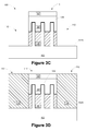
- FIG. 2C depicts the product 100 after a timed, recess etching process—a “fin reveal” etching process—was performed on the layer of insulating material 108 so as to recess the insulating material 108 to a desired height level within the trenches 105 .
- the layer of insulating material 108 has a recessed upper surface 108 R that exposes the desired final fin height of the fins 106 above the insulating material 108 .
- FIG. 2D depicts the product 100 after several process operations were performed.
- a conformal deposition process such as an ALD process, was performed to form a relatively thin (e.g., 2-4 nm) conformal layer of silicon dioxide (not shown) on the recessed upper surface 108 R of the layer of insulating material 108 , on the sidewalls of the fins 106 and around the features of the patterned fin-formation hard mask 104 .
- a sacrificial layer of material 110 was formed so as to over-fill the remaining portions of the trenches 105 such that its upper surface 110 S is positioned at a level that is above the level of the upper surface 104 S of the patterned fin-formation hard mask 104 .
- a CMP process may be performed on the layer of material 110 if desired.
- the layer of material 110 should be made of a material that exhibits good etch selectivity to silicon dioxide, a material such as silicon nitride, silicon oxynitride, SiBCN, etc.
- the next major process operation involves removing portions of the fins 106 so as to define an isolation region opening 112 where a device isolation structure will be formed around the perimeter of the FinFET device.
- a patterned masking layer (not shown), e.g., a patterned layer of photoresist, that was formed above the sacrificial layer of material 110 .
- the patterned masking layer covers the area above the portions of the fins 106 A-C that will become the active fins of the FinFET device.
- the patterned masking layer also has an opening that is located above an area where portions of the laterally adjacent fins 106 D-G and portions of the fins 106 A-C will be removed to define the isolation region opening 112 for the device isolation region that will be formed around the perimeter of the FinFET device.
- a first etching process was performed through the patterned masking layer to remove the portion of the sacrificial layer of material 110 , the portion of the silicon dioxide liner layer (not shown) and the portion of the patterned fin formation masking layer 104 positioned under the opening in the patterned masking layer.
- the first etching process stops on the insulation material 108 .
- This first etching process results in the formation of a patterned fin masking layer 111 .
- the patterned fin masking layer 111 comprises portions of the sacrificial layer of material 110 .
- the patterned fin masking layer 111 is positioned above or covers the portions of the fins 106 A-C that will become part of the FinFET device and contains an opening that corresponds to the isolation region opening 112 where the device isolation region will be formed, i.e., the pattern in the patterned masking layer is transferred to the patterned fin masking layer 111 .
- the patterned masking layer may be removed.
- a second etching process was performed to remove the exposed portions of the fins 106 within the isolation region opening 112 .
- the entire vertical height of the exposed portions of the fins 106 was removed.
- a third etching process was performed to remove the exposed portions of the insulation material 108 within the isolation region opening 112 . The result of all of these process operations is that the isolation region opening 112 for a device isolation region is formed around the perimeter of the FinFET device and that portions of the upper surface 102 S of the substrate 102 is exposed.
- FIG. 2F is a simplistic plan view of the product 100 after the fins 106 have been cut and removed.
- FIG. 2F does not depict any of the various layers of material present above the substrate 102 , only the fins 106 and the substrate 102 are depicted.
- FIG. 2G is a simplistic plan view of the product 100 wherein the patterned fin masking layer 111 (i.e., the remaining portions of the sacrificial layer of material 110 ) is depicted and wherein the remaining fins 106 are depicted in dashed lines.
- the patterned fin masking layer 111 i.e., the remaining portions of the sacrificial layer of material 110
- the illustrative active fins 106 A, 106 B and 106 C for the FinFET device will have been cut to the desired final axial length.
- FIG. 2H depicts the product 100 after several process operations were performed.
- a layer of insulating material 114 was deposited so as to over-fill the isolation region opening 112 for the device isolation region.
- a planarization process such as a CMP process, was performed on the layer of insulating material 114 that stopped on the upper surface of the patterned fin masking layer 111 .
- the layer of insulating material 114 may be comprised of a material that is the same as that of the layer of insulating material 108 , e.g., they both may be silicon dioxide, but, in some applications, the materials of the layers 108 , 114 may be different.
- FIG. 2I depicts the product 100 after a timed, recess etching process was performed on the layer of insulating material 114 so as to recess the insulating material 114 to a desired height level within the isolation region opening 112 .
- the layer of insulating material 114 has a recessed upper surface 114 R.
- the amount of recessing of the layer of insulation material 114 may vary depending upon the particular application.
- the layer of insulting material 114 may be recessed such that its recessed upper surface 114 R is positioned at the level indicated by the dashed line 114 X.
- FIG. 2J depicts the product 100 after a conformal deposition process, such as an ALD process, was performed to form a relatively thin (e.g., 2-4 nm) conformal layer of silicon dioxide 116 on the recessed upper surface 114 R of the layer of insulating material 114 and on the upper surface and sides of the patterned fin masking layer 111 .
- a conformal deposition process such as an ALD process
- FIG. 2K depicts the product 100 after several process operations were performed.
- a directional deposition process such as a gas cluster ion beam (GCIB) process, was performed to form a layer of isolation protection material 118 on the substantially horizontally oriented surfaces, i.e., to form a first portion of the isolation protection material 118 above the patterned fin masking layer 111 and to form a second portion of the isolation protection material 118 in the isolation region opening 112 above the layer of silicon dioxide 116 .
- GCIB gas cluster ion beam
- the thickness of the layer of isolation protection material 118 may vary depending upon the particular application, e.g., 10-30 nm.
- the layer of isolation protection material 118 should be made of a material that exhibits good etch selectivity to silicon dioxide, e.g., a material such as silicon nitride, silicon oxynitride, SiBCN, etc.
- the layer of isolation protection material 118 may be comprised of a material that is the same as that of the sacrificial layer of material 110 , e.g., they both may be made of silicon nitride, but, in some applications, the materials of the layers 118 , 110 may be different.
- the layer of isolation protection material 118 After forming the layer of isolation protection material 118 , another conformal deposition process, such as an ALD process, was performed to form a relatively thin (e.g., 2-4 nm) conformal layer of material 120 .
- the conformal layer of material 120 is depicted with a dashed line so as to distinguish it from the conformal layer of silicon dioxide 116 .
- the conformal layer of material 120 should be made of a material that may be selectively etched relative to the layer of isolation protection material 118 and the conformal layer of silicon dioxide 116 .
- the conformal layer of material 120 may be comprised of a material having a dielectric constant greater than about 10, e.g., hafnium oxide, etc.
- FIG. 2L depicts the product 100 after several process operations were performed.
- a layer of masking material 122 such as SOH, OPL, etc., was deposited so as to substantially fill the remaining portions of the isolation region opening 112 .
- a timed, recess etching process was performed on the layer of masking material 122 such that it has a recessed upper surface 122 R.
- the amount of recessing of the layer of masking material 122 may vary depending upon the particular application. In general, the recessed upper surface 122 R should be positioned at level that is below the upper surface of the patterned fin masking layer 111 .
- FIG. 2M depicts the product after several process operations were performed.
- an etching process was performed to remove exposed portions of the conformal layer of material 120 .
- the etching process exposes the portion of the layer of isolation protection material 118 positioned above the patterned fin masking layer 111 and above the fins 106 .
- another etching process was performed to remove the exposed first portion of the layer of isolation protection material 118 .
- another etching process was performed to remove the exposed portions of the conformal layer of silicon dioxide 116 .
- FIG. 2N depicts the product after an etching process was performed to remove the layer of masking material 122 .
- FIG. 2O depicts the product 100 after several processing operations were performed.
- an etching process was performed to remove the patterned fin masking layer 111 .
- the patterned fin-formation masking layer 104 is protected by a thin conformal layer of silicon dioxide (not shown).
- a brief etching process is performed to remove the conformal layer of silicon dioxide and thereby expose the patterned fin-formation masking layer 104 .
- another etching process was performed to remove the patterned fin-formation masking layer 104 and to expose the upper surface and sidewalls of the fins 106 A-C.
- FIG. 2P depicts the product after one or more etching processes were performed to remove the exposed portion of the conformal layer of silicon dioxide 116 and the conformal layer of material 120 .
- the remaining portions of the layer of isolation protection material 118 constitute an isolation protection layer 125 that is positioned above an isolation region 127 .
- the isolation region 127 comprises at least the insulating material 114 positioned in the isolation region opening 112 .
- FIG. 2Q depicts the product after an illustrative and representative gate structure 130 , a gate cap layer 132 and a sidewall spacer 134 were formed.
- the materials of construction for the gate structure 130 of an NMOS device may be (and likely will be) different from the gate structure of a PMOS device.
- the schematically depicted gate structure 130 includes an illustrative gate insulation layer 130 A and an illustrative gate electrode 130 B.
- the gate insulation layer 130 A may be comprised of a variety of different materials, such as, for example, silicon dioxide, a so-called high-k (k greater than 10) insulation material (where k is the relative dielectric constant), etc.
- the gate electrode 130 B may also be of a material such as polysilicon or amorphous silicon, or it may be comprised of one or more metal layers that act as the gate electrode 130 B.
- the gate structure 130 of the FinFET device depicted in the drawings i.e., the gate insulation layer 130 A and the gate electrode 130 B are intended to be representative in nature.
- the gate structure 130 may be comprised of a variety of different materials and it may have a variety of configurations.
- the gate structure 130 may be manufactured using either the so-called “gate-first” or “replacement gate” techniques.
- other processing activities may also be performed, e.g., the formation of doped halo implant regions (not shown), doped source/drain regions (not shown), the formation of epi semiconductor material (not shown) in the source/drain regions, etc. As depicted in FIG.
- a notch or recess 125 X is formed in the isolation protection layer 125 when the anisotropic etching process is performed to form the spacer 134 , such that the isolation protection layer 125 has a stepped configuration due to the presence of the notch 125 X. That is, in the cross-sectional view shown in FIG.
- the portions of the isolation protection layer 125 positioned under the sidewall spacer 134 and the gate structure 130 are thicker than the portions of the isolation protection layer 125 not covered the spacer 134 and the gate structure 130 .
- the isolation protection layer 125 also has this same stepped configuration when viewed in a cross-section taken through a fin and the gate in a gate length direction of the device.
- the “fin-reveal” process i.e., the recessing of the layer of insulating material 108 , was performed prior to removing the fins in the areas occupied by the device isolation region 127 .
- FIG. 2R is a simplistic plan view of the product 100 after the gate has been formed.
- the isolation protection layer 125 is positioned above the insulating material 114 that constitutes the device isolation structure 127 .
- the isolation protection layer 125 may be comprised of silicon nitride so as to protect the underlying silicon dioxide insulation material 114 in the device isolation structure 127 as subsequent processing proceeds on the device, thereby eliminating or at least reducing the formation of the divots in the isolation material as discussed in the background section of this application.
- FIGS. 3A-3I depict other illustrative novel methods disclosed herein for forming a protection layer on an isolation region of integrated circuit (IC) products comprising FinFET devices.
- FIG. 3A depicts the device at a point in processing that corresponds to that shown in FIG. 2C , i.e., after the above-described timed, recess etching process was performed on the layer of insulating material 108 so as to recess the insulating material 108 to a desired height level within the trenches 105 .
- FIG. 3B depicts the product 100 after several process operations were performed.
- an etching process was performed to remove the patterned fin formation hard mask 104 .
- a conformal deposition process such as an ALD process, was performed to form a relatively thin (e.g., 2-4 nm) conformal layer of silicon dioxide 138 .
- a sacrificial layer of material 140 such as amorphous silicon or polysilicon, and a sacrificial layer of material 142 , e.g., silicon nitride, was blanket-deposited across the substrate 102 .
- the materials 140 , 142 may be formed to any desired thickness.
- FIG. 3C depicts the product 100 after the above-described masking and etching processes were performed to remove various layers of material and portions of the fins 106 so as to define the isolation region opening 112 where the device isolation structure 127 will be formed around the FinFET device.
- a first etching process was performed through a patterned masking layer (not shown), e.g., a patterned layer of photoresist, to remove the exposed portions of sacrificial layer 142 .
- the patterned masking layer may be removed at this point in the process flow if desired.
- another etching process was performed to remove the exposed portions of the sacrificial layer of material 140 that stops on the silicon dioxide liner layer 138 .
- the patterned fin masking layer 111 comprises a portion of the sacrificial layer of material 142 and a portion of the sacrificial layer of material 140 .
- etching process was performed to remove the silicon dioxide liner layer 138 and expose the portions of the fins 106 that are to be removed. This latter etching process stops on the portions of the insulation material 108 positioned within the isolation region opening 112 . Then, yet another etching process was performed to remove the exposed portions of the fins 106 . In the depicted example, the entire vertical height of the exposed portions of the fins 106 was removed. Next, a final etching process was performed to remove the exposed portions of the insulation material 108 . The result of all of these process operations is that the isolation region opening 112 for the device isolation region 127 is formed around the perimeter of the FinFET device and exposes portions of the upper surface 102 S of the substrate 102 .
- FIG. 3D depicts the product 100 after the above-described layer of insulating material 114 was formed in the isolation region opening 112 and after a CMP process was performed on the layer of insulating material 114 that stopped on the upper surface of the sacrificial layer of material 142 .
- FIG. 3E depicts the product 100 after the above-described timed, recess etching process was performed to recess the layer of insulating material 114 to a desired height level within the isolation region opening 112 .
- FIG. 3F depicts the product 100 after the above-described directional deposition process, such as a gas cluster ion beam (GCIB) process, was performed to form the above-described layer of isolation protection material 118 on the substantially horizontally oriented surfaces, i.e., to form a first portion above the patterned fin masking layer 111 and to form a second portion of the isolation protection material 118 in the isolation region opening 112 above the layer of silicon dioxide 114 .
- GCIB gas cluster ion beam
- FIG. 3G depicts the product 100 after the above-described layer of masking material 122 , such as SOH, OPL, etc., was deposited so as to substantially fill the remaining portions of the isolation region opening 112 and after the above-described timed, recess etching process was performed on the layer of masking material 122 such that it has a recessed upper surface 122 R that, in one embodiment, is positioned at a level that is above the upper surface 140 R of the layer of sacrificial material 140 .
- the above-described layer of masking material 122 such as SOH, OPL, etc.
- FIG. 3H depicts the product after several process operations were performed.
- an etching process was performed to remove exposed portions of the layer of isolation protection material 118 positioned above the patterned fin masking layer 111 that is positioned above the fins 106 A-C.
- another etching process was performed to remove the layer of sacrificial material 142 selectively relative to the layer of sacrificial material 140 .
- yet another etching process was performed to remove the layer of sacrificial material 140 relative to the conformal layer of silicon dioxide 138 .
- FIG. 3I depicts the product after several process operations were performed.
- an etching process was performed to remove the layer of masking material 122 so as to expose the isolation protection layer 125 .
- another etching process was performed to remove the conformal layer of silicon dioxide 138 so as to expose the upper surface and sidewalls of the fins 106 A-C. If desired, these etching processes may be performed in any desired order.
- the FinFET device may be completed using traditional fabrication techniques. For example, the gate structure 130 , the gate cap layer 132 and sidewall spacer 134 depicted in FIG. 2Q may be formed.
- FIGS. 4A-4I depict yet other illustrative novel methods disclosed herein for forming a protection layer on an isolation region of integrated circuit (IC) products comprising FinFET devices.
- FIG. 4A depicts the device at a point in processing that corresponds to that shown in FIG. 2C , i.e., after the above-described timed, recess etching process was performed on the layer of insulating material 108 so as to recess the insulating material 108 to a desired height level within the trenches 105 .
- FIG. 4B depicts the product 100 after several process operations were performed.
- a conformal deposition process such as an ALD process, was performed to form the above-described conformal layer of silicon dioxide 138 around the fins 106 and the patterned fin-formation hard mask 104 .
- the above-described sacrificial layer of material 140 e.g., silicon nitride
- the material 140 may be formed to any desired thickness.
- FIG. 4C depicts the product 100 after the above-described masking and etching processes were performed to remove portions of various layers of material and portions of the fins 106 so as to define the isolation region opening 112 where the device isolation structure 127 will be formed around the FinFET device.
- a first etching process was performed through a patterned masking layer (not shown), e.g., a patterned layer of photoresist, to remove the exposed portions of sacrificial layer 140 .
- This process operation results in the formation of the patterned fin masking layer 111 .
- the patterned fin masking layer 111 comprises a portion of the sacrificial layer of material 140 .
- FIG. 4D depicts the product 100 after the above-described layer of insulating material 114 was formed in the isolation region opening 112 and after a CMP process was performed on the layer of insulating material 114 that stopped on the upper surface of the sacrificial layer of material 140 .
- FIG. 4E depicts the product 100 after the above-described timed, recess etching process was performed to recess the layer of insulating material 114 to a desired height level within the isolation region opening 112 .
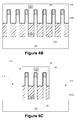
- FIG. 4F depicts the product after a conformal deposition process was performed to form a conformal layer of isolation protection material 148 above the patterned fin masking layer 111 and in the openings 112 .
- the portions of the conformal layer of isolation protection material 148 in the isolation region opening 112 will constitute the isolation protection layer 125 that is positioned above the isolation region 127 .
- the conformal layer of isolation protection material 148 may be comprised of any desired material, e.g., silicon nitride, silicon oxynitride, etc., and it may be formed to any desired thickness, e.g., 15-30 nm.
- FIG. 4G depicts the product 100 after a layer of masking material 150 , such as silicon dioxide, etc., was deposited so as to substantially fill the remaining portions of the isolation region opening 112 and after a CMP process was performed to planarize the upper surface of the layer of masking material 150 with the upper surface of the conformal layer of isolation protection material 148 .
- a layer of masking material 150 such as silicon dioxide, etc.
- FIG. 4H depicts the product 100 after a timed, recess etching process was performed to recess the layer of masking material 150 (e.g., silicon dioxide) to a desired height level within the isolation region opening 112 .
- the layer of masking material 150 may be recessed until such time as there is about 15-30 nm of the layer of masking material 150 remaining in the isolation region opening 112 above the conformal layer of isolation protection material 148 .
- FIG. 4I depicts the product after several process operations were performed. First, an etching process was performed to remove exposed portions of the layer of masking material 150 so as to expose the upper surface and sidewalls of the patterned fin masking layer 111 . Then, another etching process was performed to remove the layer of sacrificial material 140 selectively relative to the conformal layer of silicon dioxide 138 . Next, another etching process was performed to remove the conformal layer of silicon dioxide 138 and the remaining portions of the layer of masking material 150 . The removal of the conformal layer of silicon dioxide 138 exposes the upper surface and sidewalls of the fins 106 A-C.
- the remaining portions of the conformal layer of isolation protection material 148 in the isolation region opening 112 constitutes the isolation protection layer 125 that is positioned above the isolation region 127 .
- the FinFET device may be completed using traditional fabrication techniques.
- the gate structure 130 , the gate cap layer 132 and sidewall spacer 134 depicted in FIG. 2Q may be formed.
- FIG. 5 depicts one illustrative embodiment of an integrated circuit product 100 that includes FinFET devices and an isolation region 127 and one illustrative embodiment of a novel isolation protection layer 125 disclosed herein positioned above the isolation region 127 .
- FIG. 5 is a cross-sectional view taken through the fin 106 B and the gate structure 130 in a gate length (GL) direction of the device after several process operations were performed.
- FIG. 5 depicts the product 100 after the above-described isolation region 127 (comprising the insulating material 114 ) and the above-described novel isolation protection layer 125 was formed above the isolation region 127 . Thereafter, a plurality of gates 160 were formed across the substrate 102 and above the novel isolation protection layer 125 .
- the formation of the gates 160 may involve forming the materials for the gate structures 130 and the gate cap layer 132 across the product 100 and thereafter patterning those materials using traditional masking and etching processes. Thereafter, the sidewall spacer 134 may be formed by performing a conformal deposition process to form a layer of spacer material across the substrate 102 and above the novel isolation protection layer 125 and thereafter performing an anisotropic etching process to remove substantially horizontally positioned portions of the layer of spacer material. As depicted in FIG.
- a notch or recess 125 X is formed in the isolation protection layer 125 when the anisotropic etching process is performed to form the spacer 134 such that the isolation protection layer 125 has a stepped configuration due to the presence of the notch 125 X. That is, in the cross-sectional view shown in FIG.
- the portions of the isolation protection layer 125 positioned under the sidewall spacer 134 and the gate structure 130 are thicker than the portions of the isolation protection layer 125 not covered by the spacer 134 and the gate structure 130 .
- the isolation protection layer 125 also has this same stepped configuration when viewed in a cross-section taken through the gate in a gate width direction of the device.
- the isolation protection layer 125 may be comprised of silicon nitride so as to protect the underlying silicon dioxide insulation material 114 in the device isolation structure 127 as subsequent processing proceeds on the device, thereby eliminating or at least reducing the formation of the divots in the isolation material as discussed in the background section of this application.
Landscapes
- Engineering & Computer Science (AREA)
- Power Engineering (AREA)
- Microelectronics & Electronic Packaging (AREA)
- Computer Hardware Design (AREA)
- Physics & Mathematics (AREA)
- Condensed Matter Physics & Semiconductors (AREA)
- General Physics & Mathematics (AREA)
- Manufacturing & Machinery (AREA)
- Ceramic Engineering (AREA)
- Chemical & Material Sciences (AREA)
- Chemical Kinetics & Catalysis (AREA)
- General Chemical & Material Sciences (AREA)
- Inorganic Chemistry (AREA)
- Element Separation (AREA)
- Insulated Gate Type Field-Effect Transistor (AREA)
- Thin Film Transistor (AREA)
Abstract
Description
Claims (17)
Priority Applications (4)
| Application Number | Priority Date | Filing Date | Title |
|---|---|---|---|
| US15/197,944 US9876077B1 (en) | 2016-06-30 | 2016-06-30 | Methods of forming a protection layer on an isolation region of IC products comprising FinFET devices |
| TW106113770A TWI677029B (en) | 2016-06-30 | 2017-04-25 | Methods of forming a protection layer on an isolation region of ic products comprising finfet devices |
| CN201710525080.6A CN107564860B (en) | 2016-06-30 | 2017-06-30 | Method of forming a protective layer on an isolation region of an IC product including FINFET devices |
| US15/833,285 US10170544B2 (en) | 2016-06-30 | 2017-12-06 | Integrated circuit products that include FinFET devices and a protection layer formed on an isolation region |
Applications Claiming Priority (1)
| Application Number | Priority Date | Filing Date | Title |
|---|---|---|---|
| US15/197,944 US9876077B1 (en) | 2016-06-30 | 2016-06-30 | Methods of forming a protection layer on an isolation region of IC products comprising FinFET devices |
Related Child Applications (1)
| Application Number | Title | Priority Date | Filing Date |
|---|---|---|---|
| US15/833,285 Division US10170544B2 (en) | 2016-06-30 | 2017-12-06 | Integrated circuit products that include FinFET devices and a protection layer formed on an isolation region |
Publications (2)
| Publication Number | Publication Date |
|---|---|
| US20180006111A1 US20180006111A1 (en) | 2018-01-04 |
| US9876077B1 true US9876077B1 (en) | 2018-01-23 |
Family
ID=60807850
Family Applications (2)
| Application Number | Title | Priority Date | Filing Date |
|---|---|---|---|
| US15/197,944 Active US9876077B1 (en) | 2016-06-30 | 2016-06-30 | Methods of forming a protection layer on an isolation region of IC products comprising FinFET devices |
| US15/833,285 Active US10170544B2 (en) | 2016-06-30 | 2017-12-06 | Integrated circuit products that include FinFET devices and a protection layer formed on an isolation region |
Family Applications After (1)
| Application Number | Title | Priority Date | Filing Date |
|---|---|---|---|
| US15/833,285 Active US10170544B2 (en) | 2016-06-30 | 2017-12-06 | Integrated circuit products that include FinFET devices and a protection layer formed on an isolation region |
Country Status (3)
| Country | Link |
|---|---|
| US (2) | US9876077B1 (en) |
| CN (1) | CN107564860B (en) |
| TW (1) | TWI677029B (en) |
Cited By (3)
| Publication number | Priority date | Publication date | Assignee | Title |
|---|---|---|---|---|
| US10643998B2 (en) | 2017-04-03 | 2020-05-05 | Samsung Electronics Co., Ltd. | Semiconductor device having first and second fin-type patterns and method of fabricating the same |
| US10847636B2 (en) * | 2018-08-30 | 2020-11-24 | Taiwan Semiconductor Manufacturing Company Ltd. | Methods for forming semiconductor structure |
| US11018050B2 (en) | 2018-09-04 | 2021-05-25 | Samsung Electronics Co., Ltd. | Semiconductor device and method of fabricating the same |
Families Citing this family (13)
| Publication number | Priority date | Publication date | Assignee | Title |
|---|---|---|---|---|
| US9837405B1 (en) * | 2016-08-02 | 2017-12-05 | International Business Machines Corporation | Fabrication of a vertical fin field effect transistor having a consistent channel width |
| CN109390338B (en) * | 2017-08-08 | 2021-06-22 | 联华电子股份有限公司 | Complementary metal oxide semiconductor element and manufacturing method thereof |
| CN109994384B (en) * | 2017-12-29 | 2022-07-05 | 中芯国际集成电路制造(上海)有限公司 | Semiconductor structure and forming method thereof |
| CN110690285B (en) * | 2018-07-05 | 2023-12-12 | 中芯国际集成电路制造(上海)有限公司 | Semiconductor structure and forming method thereof |
| US11069693B2 (en) | 2018-08-28 | 2021-07-20 | Taiwan Semiconductor Manufacturing Co., Ltd. | Method for improving control gate uniformity during manufacture of processors with embedded flash memory |
| US10903315B2 (en) * | 2018-09-28 | 2021-01-26 | International Business Machines Corporation | Formation of dielectric layer as etch-stop for source and drain epitaxy disconnection |
| US10686033B2 (en) | 2018-11-09 | 2020-06-16 | Applied Materials, Inc. | Fin damage reduction during punch through implantation of FinFET device |
| US10692775B2 (en) * | 2018-11-09 | 2020-06-23 | Applied Materials, Inc. | Fin damage reduction during punch through implantation of FinFET device |
| KR20210056778A (en) * | 2019-11-11 | 2021-05-20 | 삼성전자주식회사 | Integrated circuit device and method of manufacturing the same |
| EP3840035A1 (en) | 2019-12-19 | 2021-06-23 | Imec VZW | A method for semiconductor device processing |
| CN113707609B (en) * | 2020-05-20 | 2023-07-18 | 长鑫存储技术有限公司 | Method for preparing semiconductor structure |
| CN113707608B (en) | 2020-05-20 | 2023-09-26 | 长鑫存储技术有限公司 | Semiconductor structure and preparation method thereof |
| KR20240013579A (en) * | 2022-07-22 | 2024-01-30 | 삼성전자주식회사 | integrated circuit semiconductor device |
Citations (1)
| Publication number | Priority date | Publication date | Assignee | Title |
|---|---|---|---|---|
| US20130277746A1 (en) * | 2012-04-24 | 2013-10-24 | Globalfoundries Inc. | Integrated circuits having protruding source and drain regions and methods for forming integrated circuits |
Family Cites Families (4)
| Publication number | Priority date | Publication date | Assignee | Title |
|---|---|---|---|---|
| US8609480B2 (en) * | 2011-12-21 | 2013-12-17 | Globalfoundries Inc. | Methods of forming isolation structures on FinFET semiconductor devices |
| US8580642B1 (en) * | 2012-05-21 | 2013-11-12 | Globalfoundries Inc. | Methods of forming FinFET devices with alternative channel materials |
| US9385123B2 (en) * | 2014-05-20 | 2016-07-05 | International Business Machines Corporation | STI region for small fin pitch in FinFET devices |
| US9478634B2 (en) * | 2014-11-07 | 2016-10-25 | Globalfoundries Inc. | Methods of forming replacement gate structures on finFET devices and the resulting devices |
-
2016
- 2016-06-30 US US15/197,944 patent/US9876077B1/en active Active
-
2017
- 2017-04-25 TW TW106113770A patent/TWI677029B/en active
- 2017-06-30 CN CN201710525080.6A patent/CN107564860B/en active Active
- 2017-12-06 US US15/833,285 patent/US10170544B2/en active Active
Patent Citations (1)
| Publication number | Priority date | Publication date | Assignee | Title |
|---|---|---|---|---|
| US20130277746A1 (en) * | 2012-04-24 | 2013-10-24 | Globalfoundries Inc. | Integrated circuits having protruding source and drain regions and methods for forming integrated circuits |
Cited By (5)
| Publication number | Priority date | Publication date | Assignee | Title |
|---|---|---|---|---|
| US10643998B2 (en) | 2017-04-03 | 2020-05-05 | Samsung Electronics Co., Ltd. | Semiconductor device having first and second fin-type patterns and method of fabricating the same |
| US10991692B2 (en) | 2017-04-03 | 2021-04-27 | Samsung Electronics Co., Ltd. | Semiconductor device having a plurality of fins and method of fabricating the same |
| US10847636B2 (en) * | 2018-08-30 | 2020-11-24 | Taiwan Semiconductor Manufacturing Company Ltd. | Methods for forming semiconductor structure |
| US11018050B2 (en) | 2018-09-04 | 2021-05-25 | Samsung Electronics Co., Ltd. | Semiconductor device and method of fabricating the same |
| US11600518B2 (en) | 2018-09-04 | 2023-03-07 | Samsung Electronics Co., Ltd. | Semiconductor device and method of fabricating the same |
Also Published As
| Publication number | Publication date |
|---|---|
| CN107564860A (en) | 2018-01-09 |
| US20180102409A1 (en) | 2018-04-12 |
| US20180006111A1 (en) | 2018-01-04 |
| US10170544B2 (en) | 2019-01-01 |
| CN107564860B (en) | 2020-05-15 |
| TW201812912A (en) | 2018-04-01 |
| TWI677029B (en) | 2019-11-11 |
Similar Documents
| Publication | Publication Date | Title |
|---|---|---|
| US9876077B1 (en) | Methods of forming a protection layer on an isolation region of IC products comprising FinFET devices | |
| US9653583B1 (en) | Methods of forming diffusion breaks on integrated circuit products comprised of finFET devices | |
| US11349013B2 (en) | IC product comprising a novel insulating gate separation structure for transistor devices | |
| US9865704B2 (en) | Single and double diffusion breaks on integrated circuit products comprised of FinFET devices | |
| US9640636B1 (en) | Methods of forming replacement gate structures and bottom and top source/drain regions on a vertical transistor device | |
| US9761495B1 (en) | Methods of performing concurrent fin and gate cut etch processes for FinFET semiconductor devices and the resulting devices | |
| US11522068B2 (en) | IC product comprising an insulating gate separation structure positioned between end surfaces of adjacent gate structures | |
| US10651293B2 (en) | Methods of simultaneously forming bottom and top spacers on a vertical transistor device | |
| US9455198B1 (en) | Methods of removing fins so as to form isolation structures on products that include FinFET semiconductor devices | |
| US20180240715A1 (en) | Methods of forming vertical transistor devices with different effective gate lengths and the resulting devices | |
| US20170154977A1 (en) | Tri-gate finfet device | |
| US9337050B1 (en) | Methods of forming fins for finFET semiconductor devices and the selective removal of such fins | |
| US9337101B1 (en) | Methods for selectively removing a fin when forming FinFET devices | |
| US9269628B1 (en) | Methods of removing portions of at least one fin structure so as to form isolation regions when forming FinFET semiconductor devices | |
| US10347745B2 (en) | Methods of forming bottom and top source/drain regions on a vertical transistor device | |
| US10431499B2 (en) | Insulating gate separation structure | |
| US9530869B2 (en) | Methods of forming embedded source/drain regions on finFET devices | |
| US10366930B1 (en) | Self-aligned gate cut isolation | |
| US10373877B1 (en) | Methods of forming source/drain contact structures on integrated circuit products | |
| US10825741B2 (en) | Methods of forming single diffusion breaks on integrated circuit products comprised of FinFET devices and the resulting products | |
| US9449881B1 (en) | Methods of forming fins for FinFET semiconductor devices and the resulting devices | |
| US9171922B1 (en) | Combination finFET/ultra-thin body transistor structure and methods of making such structures | |
| US10727133B2 (en) | Method of forming gate structure with undercut region and resulting device | |
| US20190348508A1 (en) | Methods for chamfering work function material layers in gate cavities having varying widths | |
| US9589829B1 (en) | FinFET device including silicon oxycarbon isolation structure |
Legal Events
| Date | Code | Title | Description |
|---|---|---|---|
| AS | Assignment |
Owner name: GLOBALFOUNDRIES INC., CAYMAN ISLANDS Free format text: ASSIGNMENT OF ASSIGNORS INTEREST;ASSIGNORS:XIE, RUILONG;PRINDLE, CHRISTOPHER M.;SUNG, MIN GYU;AND OTHERS;SIGNING DATES FROM 20160609 TO 20160628;REEL/FRAME:039053/0321 |
|
| STCF | Information on status: patent grant |
Free format text: PATENTED CASE |
|
| AS | Assignment |
Owner name: WILMINGTON TRUST, NATIONAL ASSOCIATION, DELAWARE Free format text: SECURITY AGREEMENT;ASSIGNOR:GLOBALFOUNDRIES INC.;REEL/FRAME:049490/0001 Effective date: 20181127 |
|
| AS | Assignment |
Owner name: GLOBALFOUNDRIES U.S. INC., CALIFORNIA Free format text: ASSIGNMENT OF ASSIGNORS INTEREST;ASSIGNOR:GLOBALFOUNDRIES INC.;REEL/FRAME:054633/0001 Effective date: 20201022 |
|
| AS | Assignment |
Owner name: GLOBALFOUNDRIES INC., CAYMAN ISLANDS Free format text: RELEASE BY SECURED PARTY;ASSIGNOR:WILMINGTON TRUST, NATIONAL ASSOCIATION;REEL/FRAME:054636/0001 Effective date: 20201117 |
|
| MAFP | Maintenance fee payment |
Free format text: PAYMENT OF MAINTENANCE FEE, 4TH YEAR, LARGE ENTITY (ORIGINAL EVENT CODE: M1551); ENTITY STATUS OF PATENT OWNER: LARGE ENTITY Year of fee payment: 4 |
|
| AS | Assignment |
Owner name: GLOBALFOUNDRIES U.S. INC., NEW YORK Free format text: RELEASE BY SECURED PARTY;ASSIGNOR:WILMINGTON TRUST, NATIONAL ASSOCIATION;REEL/FRAME:056987/0001 Effective date: 20201117 |