EP3940772A1 - Semiconductor structure and manufacturing method therefor - Google Patents
Semiconductor structure and manufacturing method therefor Download PDFInfo
- Publication number
- EP3940772A1 EP3940772A1 EP20893357.2A EP20893357A EP3940772A1 EP 3940772 A1 EP3940772 A1 EP 3940772A1 EP 20893357 A EP20893357 A EP 20893357A EP 3940772 A1 EP3940772 A1 EP 3940772A1
- Authority
- EP
- European Patent Office
- Prior art keywords
- layer
- bump
- solder
- groove
- forming
- Prior art date
- Legal status (The legal status is an assumption and is not a legal conclusion. Google has not performed a legal analysis and makes no representation as to the accuracy of the status listed.)
- Granted
Links
Images



Classifications
-
- H—ELECTRICITY
- H10—SEMICONDUCTOR DEVICES; ELECTRIC SOLID-STATE DEVICES NOT OTHERWISE PROVIDED FOR
- H10W—GENERIC PACKAGES, INTERCONNECTIONS, CONNECTORS OR OTHER CONSTRUCTIONAL DETAILS OF DEVICES COVERED BY CLASS H10
- H10W72/00—Interconnections or connectors in packages
- H10W72/30—Die-attach connectors
-
- H—ELECTRICITY
- H10—SEMICONDUCTOR DEVICES; ELECTRIC SOLID-STATE DEVICES NOT OTHERWISE PROVIDED FOR
- H10W—GENERIC PACKAGES, INTERCONNECTIONS, CONNECTORS OR OTHER CONSTRUCTIONAL DETAILS OF DEVICES COVERED BY CLASS H10
- H10W72/00—Interconnections or connectors in packages
- H10W72/20—Bump connectors, e.g. solder bumps or copper pillars; Dummy bumps; Thermal bumps
-
- H—ELECTRICITY
- H10—SEMICONDUCTOR DEVICES; ELECTRIC SOLID-STATE DEVICES NOT OTHERWISE PROVIDED FOR
- H10P—GENERIC PROCESSES OR APPARATUS FOR THE MANUFACTURE OR TREATMENT OF DEVICES COVERED BY CLASS H10
- H10P50/00—Etching of wafers, substrates or parts of devices
- H10P50/60—Wet etching
- H10P50/64—Wet etching of semiconductor materials
- H10P50/642—Chemical etching
-
- H—ELECTRICITY
- H10—SEMICONDUCTOR DEVICES; ELECTRIC SOLID-STATE DEVICES NOT OTHERWISE PROVIDED FOR
- H10W—GENERIC PACKAGES, INTERCONNECTIONS, CONNECTORS OR OTHER CONSTRUCTIONAL DETAILS OF DEVICES COVERED BY CLASS H10
- H10W72/00—Interconnections or connectors in packages
- H10W72/90—Bond pads, in general
-
- H—ELECTRICITY
- H10—SEMICONDUCTOR DEVICES; ELECTRIC SOLID-STATE DEVICES NOT OTHERWISE PROVIDED FOR
- H10W—GENERIC PACKAGES, INTERCONNECTIONS, CONNECTORS OR OTHER CONSTRUCTIONAL DETAILS OF DEVICES COVERED BY CLASS H10
- H10W72/00—Interconnections or connectors in packages
- H10W72/01—Manufacture or treatment
- H10W72/012—Manufacture or treatment of bump connectors, dummy bumps or thermal bumps
-
- H—ELECTRICITY
- H10—SEMICONDUCTOR DEVICES; ELECTRIC SOLID-STATE DEVICES NOT OTHERWISE PROVIDED FOR
- H10W—GENERIC PACKAGES, INTERCONNECTIONS, CONNECTORS OR OTHER CONSTRUCTIONAL DETAILS OF DEVICES COVERED BY CLASS H10
- H10W72/00—Interconnections or connectors in packages
- H10W72/01—Manufacture or treatment
- H10W72/012—Manufacture or treatment of bump connectors, dummy bumps or thermal bumps
- H10W72/01231—Manufacture or treatment of bump connectors, dummy bumps or thermal bumps using blanket deposition
- H10W72/01233—Manufacture or treatment of bump connectors, dummy bumps or thermal bumps using blanket deposition in liquid form, e.g. spin coating, spray coating or immersion coating
- H10W72/01235—Manufacture or treatment of bump connectors, dummy bumps or thermal bumps using blanket deposition in liquid form, e.g. spin coating, spray coating or immersion coating by plating, e.g. electroless plating or electroplating
-
- H—ELECTRICITY
- H10—SEMICONDUCTOR DEVICES; ELECTRIC SOLID-STATE DEVICES NOT OTHERWISE PROVIDED FOR
- H10W—GENERIC PACKAGES, INTERCONNECTIONS, CONNECTORS OR OTHER CONSTRUCTIONAL DETAILS OF DEVICES COVERED BY CLASS H10
- H10W72/00—Interconnections or connectors in packages
- H10W72/01—Manufacture or treatment
- H10W72/012—Manufacture or treatment of bump connectors, dummy bumps or thermal bumps
- H10W72/01231—Manufacture or treatment of bump connectors, dummy bumps or thermal bumps using blanket deposition
- H10W72/01238—Manufacture or treatment of bump connectors, dummy bumps or thermal bumps using blanket deposition in gaseous form, e.g. by CVD or PVD
-
- H—ELECTRICITY
- H10—SEMICONDUCTOR DEVICES; ELECTRIC SOLID-STATE DEVICES NOT OTHERWISE PROVIDED FOR
- H10W—GENERIC PACKAGES, INTERCONNECTIONS, CONNECTORS OR OTHER CONSTRUCTIONAL DETAILS OF DEVICES COVERED BY CLASS H10
- H10W72/00—Interconnections or connectors in packages
- H10W72/01—Manufacture or treatment
- H10W72/012—Manufacture or treatment of bump connectors, dummy bumps or thermal bumps
- H10W72/01251—Changing the shapes of bumps
-
- H—ELECTRICITY
- H10—SEMICONDUCTOR DEVICES; ELECTRIC SOLID-STATE DEVICES NOT OTHERWISE PROVIDED FOR
- H10W—GENERIC PACKAGES, INTERCONNECTIONS, CONNECTORS OR OTHER CONSTRUCTIONAL DETAILS OF DEVICES COVERED BY CLASS H10
- H10W72/00—Interconnections or connectors in packages
- H10W72/01—Manufacture or treatment
- H10W72/012—Manufacture or treatment of bump connectors, dummy bumps or thermal bumps
- H10W72/01251—Changing the shapes of bumps
- H10W72/01253—Changing the shapes of bumps by etching
-
- H—ELECTRICITY
- H10—SEMICONDUCTOR DEVICES; ELECTRIC SOLID-STATE DEVICES NOT OTHERWISE PROVIDED FOR
- H10W—GENERIC PACKAGES, INTERCONNECTIONS, CONNECTORS OR OTHER CONSTRUCTIONAL DETAILS OF DEVICES COVERED BY CLASS H10
- H10W72/00—Interconnections or connectors in packages
- H10W72/01—Manufacture or treatment
- H10W72/012—Manufacture or treatment of bump connectors, dummy bumps or thermal bumps
- H10W72/01251—Changing the shapes of bumps
- H10W72/01255—Changing the shapes of bumps by using masks
-
- H—ELECTRICITY
- H10—SEMICONDUCTOR DEVICES; ELECTRIC SOLID-STATE DEVICES NOT OTHERWISE PROVIDED FOR
- H10W—GENERIC PACKAGES, INTERCONNECTIONS, CONNECTORS OR OTHER CONSTRUCTIONAL DETAILS OF DEVICES COVERED BY CLASS H10
- H10W72/00—Interconnections or connectors in packages
- H10W72/01—Manufacture or treatment
- H10W72/019—Manufacture or treatment of bond pads
-
- H—ELECTRICITY
- H10—SEMICONDUCTOR DEVICES; ELECTRIC SOLID-STATE DEVICES NOT OTHERWISE PROVIDED FOR
- H10W—GENERIC PACKAGES, INTERCONNECTIONS, CONNECTORS OR OTHER CONSTRUCTIONAL DETAILS OF DEVICES COVERED BY CLASS H10
- H10W72/00—Interconnections or connectors in packages
- H10W72/01—Manufacture or treatment
- H10W72/019—Manufacture or treatment of bond pads
- H10W72/01931—Manufacture or treatment of bond pads using blanket deposition
- H10W72/01938—Manufacture or treatment of bond pads using blanket deposition in gaseous form, e.g. by CVD or PVD
-
- H—ELECTRICITY
- H10—SEMICONDUCTOR DEVICES; ELECTRIC SOLID-STATE DEVICES NOT OTHERWISE PROVIDED FOR
- H10W—GENERIC PACKAGES, INTERCONNECTIONS, CONNECTORS OR OTHER CONSTRUCTIONAL DETAILS OF DEVICES COVERED BY CLASS H10
- H10W72/00—Interconnections or connectors in packages
- H10W72/01—Manufacture or treatment
- H10W72/019—Manufacture or treatment of bond pads
- H10W72/01951—Changing the shapes of bond pads
-
- H—ELECTRICITY
- H10—SEMICONDUCTOR DEVICES; ELECTRIC SOLID-STATE DEVICES NOT OTHERWISE PROVIDED FOR
- H10W—GENERIC PACKAGES, INTERCONNECTIONS, CONNECTORS OR OTHER CONSTRUCTIONAL DETAILS OF DEVICES COVERED BY CLASS H10
- H10W72/00—Interconnections or connectors in packages
- H10W72/01—Manufacture or treatment
- H10W72/019—Manufacture or treatment of bond pads
- H10W72/01951—Changing the shapes of bond pads
- H10W72/01953—Changing the shapes of bond pads by etching
-
- H—ELECTRICITY
- H10—SEMICONDUCTOR DEVICES; ELECTRIC SOLID-STATE DEVICES NOT OTHERWISE PROVIDED FOR
- H10W—GENERIC PACKAGES, INTERCONNECTIONS, CONNECTORS OR OTHER CONSTRUCTIONAL DETAILS OF DEVICES COVERED BY CLASS H10
- H10W72/00—Interconnections or connectors in packages
- H10W72/071—Connecting or disconnecting
- H10W72/072—Connecting or disconnecting of bump connectors
- H10W72/07231—Techniques
- H10W72/07236—Soldering or alloying
-
- H—ELECTRICITY
- H10—SEMICONDUCTOR DEVICES; ELECTRIC SOLID-STATE DEVICES NOT OTHERWISE PROVIDED FOR
- H10W—GENERIC PACKAGES, INTERCONNECTIONS, CONNECTORS OR OTHER CONSTRUCTIONAL DETAILS OF DEVICES COVERED BY CLASS H10
- H10W72/00—Interconnections or connectors in packages
- H10W72/071—Connecting or disconnecting
- H10W72/072—Connecting or disconnecting of bump connectors
- H10W72/07251—Connecting or disconnecting of bump connectors characterised by changes in properties of the bump connectors during connecting
- H10W72/07253—Connecting or disconnecting of bump connectors characterised by changes in properties of the bump connectors during connecting changes in shapes
-
- H—ELECTRICITY
- H10—SEMICONDUCTOR DEVICES; ELECTRIC SOLID-STATE DEVICES NOT OTHERWISE PROVIDED FOR
- H10W—GENERIC PACKAGES, INTERCONNECTIONS, CONNECTORS OR OTHER CONSTRUCTIONAL DETAILS OF DEVICES COVERED BY CLASS H10
- H10W72/00—Interconnections or connectors in packages
- H10W72/071—Connecting or disconnecting
- H10W72/072—Connecting or disconnecting of bump connectors
- H10W72/07251—Connecting or disconnecting of bump connectors characterised by changes in properties of the bump connectors during connecting
- H10W72/07254—Connecting or disconnecting of bump connectors characterised by changes in properties of the bump connectors during connecting changes in dispositions
-
- H—ELECTRICITY
- H10—SEMICONDUCTOR DEVICES; ELECTRIC SOLID-STATE DEVICES NOT OTHERWISE PROVIDED FOR
- H10W—GENERIC PACKAGES, INTERCONNECTIONS, CONNECTORS OR OTHER CONSTRUCTIONAL DETAILS OF DEVICES COVERED BY CLASS H10
- H10W72/00—Interconnections or connectors in packages
- H10W72/20—Bump connectors, e.g. solder bumps or copper pillars; Dummy bumps; Thermal bumps
- H10W72/221—Structures or relative sizes
-
- H—ELECTRICITY
- H10—SEMICONDUCTOR DEVICES; ELECTRIC SOLID-STATE DEVICES NOT OTHERWISE PROVIDED FOR
- H10W—GENERIC PACKAGES, INTERCONNECTIONS, CONNECTORS OR OTHER CONSTRUCTIONAL DETAILS OF DEVICES COVERED BY CLASS H10
- H10W72/00—Interconnections or connectors in packages
- H10W72/20—Bump connectors, e.g. solder bumps or copper pillars; Dummy bumps; Thermal bumps
- H10W72/221—Structures or relative sizes
- H10W72/222—Multilayered bumps, e.g. a coating on top and side surfaces of a bump core
-
- H—ELECTRICITY
- H10—SEMICONDUCTOR DEVICES; ELECTRIC SOLID-STATE DEVICES NOT OTHERWISE PROVIDED FOR
- H10W—GENERIC PACKAGES, INTERCONNECTIONS, CONNECTORS OR OTHER CONSTRUCTIONAL DETAILS OF DEVICES COVERED BY CLASS H10
- H10W72/00—Interconnections or connectors in packages
- H10W72/20—Bump connectors, e.g. solder bumps or copper pillars; Dummy bumps; Thermal bumps
- H10W72/221—Structures or relative sizes
- H10W72/224—Bumps having multiple side-by-side cores
-
- H—ELECTRICITY
- H10—SEMICONDUCTOR DEVICES; ELECTRIC SOLID-STATE DEVICES NOT OTHERWISE PROVIDED FOR
- H10W—GENERIC PACKAGES, INTERCONNECTIONS, CONNECTORS OR OTHER CONSTRUCTIONAL DETAILS OF DEVICES COVERED BY CLASS H10
- H10W72/00—Interconnections or connectors in packages
- H10W72/20—Bump connectors, e.g. solder bumps or copper pillars; Dummy bumps; Thermal bumps
- H10W72/231—Shapes
- H10W72/234—Cross-sectional shape, i.e. in side view
-
- H—ELECTRICITY
- H10—SEMICONDUCTOR DEVICES; ELECTRIC SOLID-STATE DEVICES NOT OTHERWISE PROVIDED FOR
- H10W—GENERIC PACKAGES, INTERCONNECTIONS, CONNECTORS OR OTHER CONSTRUCTIONAL DETAILS OF DEVICES COVERED BY CLASS H10
- H10W72/00—Interconnections or connectors in packages
- H10W72/20—Bump connectors, e.g. solder bumps or copper pillars; Dummy bumps; Thermal bumps
- H10W72/241—Dispositions, e.g. layouts
- H10W72/244—Dispositions, e.g. layouts relative to underlying supporting features, e.g. bond pads, RDLs or vias
-
- H—ELECTRICITY
- H10—SEMICONDUCTOR DEVICES; ELECTRIC SOLID-STATE DEVICES NOT OTHERWISE PROVIDED FOR
- H10W—GENERIC PACKAGES, INTERCONNECTIONS, CONNECTORS OR OTHER CONSTRUCTIONAL DETAILS OF DEVICES COVERED BY CLASS H10
- H10W72/00—Interconnections or connectors in packages
- H10W72/20—Bump connectors, e.g. solder bumps or copper pillars; Dummy bumps; Thermal bumps
- H10W72/251—Materials
- H10W72/252—Materials comprising solid metals or solid metalloids, e.g. PbSn, Ag or Cu
-
- H—ELECTRICITY
- H10—SEMICONDUCTOR DEVICES; ELECTRIC SOLID-STATE DEVICES NOT OTHERWISE PROVIDED FOR
- H10W—GENERIC PACKAGES, INTERCONNECTIONS, CONNECTORS OR OTHER CONSTRUCTIONAL DETAILS OF DEVICES COVERED BY CLASS H10
- H10W72/00—Interconnections or connectors in packages
- H10W72/20—Bump connectors, e.g. solder bumps or copper pillars; Dummy bumps; Thermal bumps
- H10W72/251—Materials
- H10W72/255—Materials of outermost layers of multilayered bumps, e.g. material of a coating
-
- H—ELECTRICITY
- H10—SEMICONDUCTOR DEVICES; ELECTRIC SOLID-STATE DEVICES NOT OTHERWISE PROVIDED FOR
- H10W—GENERIC PACKAGES, INTERCONNECTIONS, CONNECTORS OR OTHER CONSTRUCTIONAL DETAILS OF DEVICES COVERED BY CLASS H10
- H10W72/00—Interconnections or connectors in packages
- H10W72/20—Bump connectors, e.g. solder bumps or copper pillars; Dummy bumps; Thermal bumps
- H10W72/281—Auxiliary members
- H10W72/287—Flow barriers
-
- H—ELECTRICITY
- H10—SEMICONDUCTOR DEVICES; ELECTRIC SOLID-STATE DEVICES NOT OTHERWISE PROVIDED FOR
- H10W—GENERIC PACKAGES, INTERCONNECTIONS, CONNECTORS OR OTHER CONSTRUCTIONAL DETAILS OF DEVICES COVERED BY CLASS H10
- H10W72/00—Interconnections or connectors in packages
- H10W72/20—Bump connectors, e.g. solder bumps or copper pillars; Dummy bumps; Thermal bumps
- H10W72/29—Bond pads specially adapted therefor
-
- H—ELECTRICITY
- H10—SEMICONDUCTOR DEVICES; ELECTRIC SOLID-STATE DEVICES NOT OTHERWISE PROVIDED FOR
- H10W—GENERIC PACKAGES, INTERCONNECTIONS, CONNECTORS OR OTHER CONSTRUCTIONAL DETAILS OF DEVICES COVERED BY CLASS H10
- H10W72/00—Interconnections or connectors in packages
- H10W72/90—Bond pads, in general
- H10W72/921—Structures or relative sizes of bond pads
- H10W72/923—Bond pads having multiple stacked layers
-
- H—ELECTRICITY
- H10—SEMICONDUCTOR DEVICES; ELECTRIC SOLID-STATE DEVICES NOT OTHERWISE PROVIDED FOR
- H10W—GENERIC PACKAGES, INTERCONNECTIONS, CONNECTORS OR OTHER CONSTRUCTIONAL DETAILS OF DEVICES COVERED BY CLASS H10
- H10W72/00—Interconnections or connectors in packages
- H10W72/90—Bond pads, in general
- H10W72/931—Shapes of bond pads
- H10W72/934—Cross-sectional shape, i.e. in side view
-
- H—ELECTRICITY
- H10—SEMICONDUCTOR DEVICES; ELECTRIC SOLID-STATE DEVICES NOT OTHERWISE PROVIDED FOR
- H10W—GENERIC PACKAGES, INTERCONNECTIONS, CONNECTORS OR OTHER CONSTRUCTIONAL DETAILS OF DEVICES COVERED BY CLASS H10
- H10W72/00—Interconnections or connectors in packages
- H10W72/90—Bond pads, in general
- H10W72/941—Dispositions of bond pads
- H10W72/9415—Dispositions of bond pads relative to the surface, e.g. recessed, protruding
-
- H—ELECTRICITY
- H10—SEMICONDUCTOR DEVICES; ELECTRIC SOLID-STATE DEVICES NOT OTHERWISE PROVIDED FOR
- H10W—GENERIC PACKAGES, INTERCONNECTIONS, CONNECTORS OR OTHER CONSTRUCTIONAL DETAILS OF DEVICES COVERED BY CLASS H10
- H10W72/00—Interconnections or connectors in packages
- H10W72/90—Bond pads, in general
- H10W72/951—Materials of bond pads
- H10W72/952—Materials of bond pads comprising metals or metalloids, e.g. PbSn, Ag or Cu
-
- H—ELECTRICITY
- H10—SEMICONDUCTOR DEVICES; ELECTRIC SOLID-STATE DEVICES NOT OTHERWISE PROVIDED FOR
- H10W—GENERIC PACKAGES, INTERCONNECTIONS, CONNECTORS OR OTHER CONSTRUCTIONAL DETAILS OF DEVICES COVERED BY CLASS H10
- H10W74/00—Encapsulations, e.g. protective coatings
- H10W74/10—Encapsulations, e.g. protective coatings characterised by their shape or disposition
- H10W74/131—Encapsulations, e.g. protective coatings characterised by their shape or disposition the semiconductor body being only partially enclosed
- H10W74/147—Encapsulations, e.g. protective coatings characterised by their shape or disposition the semiconductor body being only partially enclosed the encapsulations being multilayered
-
- H—ELECTRICITY
- H10—SEMICONDUCTOR DEVICES; ELECTRIC SOLID-STATE DEVICES NOT OTHERWISE PROVIDED FOR
- H10W—GENERIC PACKAGES, INTERCONNECTIONS, CONNECTORS OR OTHER CONSTRUCTIONAL DETAILS OF DEVICES COVERED BY CLASS H10
- H10W90/00—Package configurations
- H10W90/701—Package configurations characterised by the relative positions of pads or connectors relative to package parts
- H10W90/721—Package configurations characterised by the relative positions of pads or connectors relative to package parts of bump connectors
- H10W90/724—Package configurations characterised by the relative positions of pads or connectors relative to package parts of bump connectors between a chip and a stacked insulating package substrate, interposer or RDL
Definitions
- the present disclosure relates to the field of semiconductor technology, and in particular to a semiconductor structure and a manufacturing method thereof.
- solder can creep if the amount of solder is not enough to weld, causing the problem of surface non-wetting, or solder bridging between blocks can occur if there is too much solder.
- a semiconductor structure comprising: a semiconductor substrate; a metal pad, disposed on the semiconductor substrate; a bump, disposed on the metal pad; a barrier layer, disposed on a side of the bump away from the metal pad, the barrier layer includes a first surface and a second surface; a first solder layer, disposed between the bump and the first surface of the barrier layer; and a second solder layer, disposed on the second surface of the barrier layer.
- the barrier layer comprises a first groove, a notch of the first groove faces a direction away from the first solder layer, and the second solder layer is disposed in the first groove, part of the second solder layer protrudes from the first groove; and/or the barrier layer further comprises a second groove, and the first solder layer is disposed in the second groove.
- a cross section of the barrier layer has an H-shape.
- the barrier layer and the bump are spaced apart and the first solder layer is provided between the barrier layer and the bump.
- the second solder layer is provided in the first groove, and/or the first solder layer is provided in the second groove.
- the first groove and the second groove are both semi-closed grooves.
- a distance between a bottom surface of the second groove and a top surface of the bump is in a range of 5um to50um.
- a depth of the first groove is greater than a depth of the second groove.
- the bump comprises a copper pillar
- the semiconductor structure further comprises: an under-bump metal layer, at least part of the under-bump metal layer is sandwiched between the metal pad and the bump.
- the semiconductor structure further comprises: a first protection layer, disposed on the semiconductor substrate, the first protection layer comprises a first opening, and the first opening exposes part of the metal pad.
- the semiconductor structure further comprises: a second protective layer, disposed on the first protective layer, the second protective layer comprises a second opening, a diameter of the second opening is smaller than or equal to a diameter of the first opening; and wherein the under-bump metal layer at least covers a bottom surface and sidewall surfaces of the second opening, and at least part of the under-bump metal layer is disposed in the second opening.
- a method of manufacturing a semiconductor structure comprising: providing a semiconductor substrate, and forming a metal pad on the semiconductor substrate; forming a bump on the metal pad; forming a first solder layer on a side of the bump away from the metal pad; forming a barrier layer on a side of the first solder layer away from the bump; and forming a second solder layer on a side of the barrier layer away from the first solder layer.
- the barrier layer comprises a first groove and a second groove separated from each other, a notch of the first groove faces a direction away from the first solder layer, the first solder layer is arranged in the second groove, the second solder layer is formed in the first groove, and part of the second solder layer protrudes from the notch of the first groove.
- the manufacturing method before forming the bump, further comprises: forming an under-bump metal layer on the metal pad, wherein at least part of the under-bump metal layer is sandwiched between the metal pad and the bump.
- the manufacturing method before forming the bump, further comprises: forming a first protective layer on the semiconductor substrate, wherein the first protection layer has a first opening, and the first opening exposes part of the metal pad.
- the manufacturing method further comprises: forming a second protective layer on an upper surface of the first protective layer and an upper surface of the metal pad; after forming the second protection layer, forming the under-bump metal layer on the metal pad and the second protection layer; wherein the second protection layer comprises a second opening, a diameter of the second opening is smaller than or equal to a diameter of the first opening; and the under-bump metal layer at least covers a bottom surface and sidewall surfaces of the second opening and at least part of the under-bump metal layer is disposed in the second opening.
- the manufacturing method before forming the bump, further comprises: forming a first photoresist layer on the semiconductor substrate except positions corresponding to the bump and the first solder layer; and removing the first photoresist layer after forming the bump and the first solder layer.
- the manufacturing method before forming the barrier layer, further comprises: forming a first mask layer on the semiconductor substrate on which the first solder layer is formed; photoetching the first mask layer by a photolithography process to expose part of the first solder layer; etching the part of the first solder layer by a chemical acid etching process, and then removing the first mask layer; forming a second mask layer; photoetching the second mask layer by a photolithography process to expose the first solder layer, the barrier layer is formed on the first solder layer and the second mask layer, wherein the first solder layer is arranged between the barrier layer and the bump.
- the manufacturing method further comprises: forming a second photoresist layer on the barrier layer at a position corresponding to the first solder layer; etching the barrier layer at a position not covered by the second photoresist layer; removing the second photoresist layer; filling solder in the first groove to form the second solder layer; and removing the second mask layer.
- the manufacturing method further comprises: forming a third photoresist layer on the barrier layer except a position corresponding to the first solder layer; filling solder in the first groove to form the second solder layer; removing the third photoresist layer; etching the barrier layer at a position not covered by solder; and removing the second mask layer.
- the semiconductor structure of the present disclosure includes a semiconductor substrate, a metal pad, a bump, a first solder layer, a barrier layer, and a second solder layer.
- the metal pad is disposed on the upper surface of the semiconductor substrate, and then the bump, the first solder layer, a barrier layer, and a second solder layer are sequentially disposed upwards. Since the second solder layer and the first solder layer are respectively arranged on two sides of the barrier layer, the problem of non-wetting caused by insufficient solder amount during the flip-chip soldering process can be mitigated.
- the reference numerals are explained as follows: 1. package substrate; 10, metal pad; 11, first photoresist layer; 12, first mask layer; 13, second mask layer; 14, second photoresist layer; 20, semiconductor substrate; 30, bump; 40, first solder layer; 41, removal space; 50, barrier layer; 51, first groove; 52, second groove; 60, second solder layer; 70, metal layer under-bump; 80, the first protective layer; 90, the second protective layer.
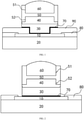
- the semiconductor structure includes: a semiconductor substrate 20; a metal pad 10 disposed on the semiconductor substrate 20; a bump 30 disposed on the metal pad 10; a barrier layer 50 is disposed at the side of the bump 30 away from the metal pad 10, the barrier layer 50 includes a first surface facing down and a second surface facing up; the first solder layer 40 is disposed between the bump 30 and the first surface of the barrier layer 50; and the second solder layer 60 is disposed on the second surface of the barrier layer 50.
- the semiconductor structure of an embodiment of the present disclosure is composed of a semiconductor substrate 20, a metal pad 10, a bump 30, a first solder layer 40, a barrier layer 50, and a second solder layer 60.
- the metal pad 10 is disposed onan upper surface of the semiconductor substrate 20.
- the surface is then provided with a bump 30, a first solder layer 40, a barrier layer 50, and a second solder layer 60 in an upwards order. Since the second solder layer 60 and the first solder layer 40 are respectively disposed on two sides of the barrier layer 50, the problem of surface non-wetting caused by insufficient solder amount during the flip-chip soldering process can be mitigated.
- the barrier layer 50 has a first groove 51, the notch of the first groove 51 faces away from the first solder layer 40, the second solder layer 60 is disposed in the first groove 51, and part of the second solder layer 60 protrudes from the notch of the first groove 51; and/or the barrier layer 50 has a second groove 52, and the first solder layer 40 is disposed in the second groove 52, the first surface of the barrier layer is the bottom surface of the second groove 52, and the second surface of the barrier layer is the bottom surface of the first groove 51. From the arrangement of the first groove 51 and/or the second groove 52, during the flip-chip reflow process, the barrier layer 50 can block the flow of the solder and play a role of drainage.
- the semiconductor structure includes: a semiconductor substrate 20; a metal pad 10 arranged on the semiconductor substrate 20; a bump 30 arranged on the metal pad 10; a first solder layer 40, arranged on the side of the bump 30 away from the metal pad 10; the barrier layer 50 is arranged on the side of the first solder layer 40 away from the bump 30, the barrier layer 50 has a first groove 51 and a second groove 52, the notch of the first groove 51 faces away from the first solder layer 40, the first solder layer 40 is arranged in the second groove 52; the second solder layer 60 is arranged in the first groove 51, part of the second solder layer 60 protrudes from the notch of the first groove 51.
- the semiconductor structure of an embodiment of the present disclosure is composed of a semiconductor substrate 20, a metal pad 10, a bump 30, a first solder layer 40, a barrier layer 50, and a second solder layer 60.
- the metal pad 10 is disposed on an upper surface of the semiconductor substrate 20.
- the surface of the metal pad 10 is then provided with a bump 30, a first solder layer 40, a barrier layer 50, and a second solder layer 60 in an upward order. Since the second solder layer 60 and the first solder layer 40 are tucked in the barrier layer 50, the non-wetting problem caused by insufficient solder and solder bridging caused by excessive solder volume are both improved during the flip-chip soldering process.
- the semiconductor structure is a stretchable metal.
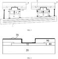
- the package substrate 1 is heated and warped, and the first solder layer 40 has gone through reflow at a high temperature, melted and stretchable. Therefore, the height adjustment is automatically performed, which can reduce the non-wetting problem caused by the deformation of the package substrate 1 after reflow.
- the first groove 51 and the second groove 52 of the barrier layer 50 each have only one opening, that is, the first groove 51 and the second groove 52 are both semi-closed grooves.
- the barrier layer 50 can block the flow of the solder and play a role of drainage, so that the second solder layer 60 does not diffuse in large amounts, which avoids the problem of solder bridging, meeting the goal of improving the yield.
- the distance between the bottom surface of the second groove 52 and the top surface of the bump 30 is 5um-50um, that is, the thickness of the first solder layer 40 between the bottom surface of the second groove 52 and the top surface of the bump 30 ranges from 5um to 50um. Further, the distance between the bottom surface of the second groove 52 and the top surface of the bump 30 is 15um-35um. Optionally, the distance between the bottom surface of the second groove 52 and the top surface of the bump 30 is about 5um, 10 um, 13 um, 15um, 20 um, 30 um, 35um, 40 um, 42 um or 50um.
- the depth of the first groove 51 is greater than the depth of the second groove 52, that is, the thickness of the second solder layer 60 located in the first groove 51 is greater than the thickness of the solder layer 40 located in the first groove 51.
- the material of the first solder layer 40 and the second solder layer 60 may include one of lead, tin, and silver and an alloy containing any one of the foregoing solder metals.
- the material of the first solder layer 40 and/or the second solder layer 60 may be an alloy with a tin content of 91.5% to 98.5% and a silver content of 8.5% to 1.5%.
- the material of the first solder layer 40 and/or the second solder layer 60 may be an alloy with a tin content of 93.2% to 96.5% and a silver content of 6.8% to 3.5%
- the material of the first solder layer 40, and/ or the second solder layer 60 may be an alloy with a tin content of 98.2% to 98.5% and a silver content of 1.8% to 1.5%.
- the semiconductor base 20 includes a semiconductor substrate and a number of IC circuits and insulating layers.
- the material of the metal pad 10 may be aluminum or copper, but is not limited thereto.
- the cross section of the barrier layer 50 is H-shaped.
- the cross section of the barrier layer 50 can be understood as a longitudinal cross section of the barrier layer 50 with reference to FIG. 1 and FIG. 2 .
- the barrier layer 50 is a barrel-shaped structure with a separator in the middle, and the second solder layer 60 and the first solder layer 40 are not in direct contact with each other.
- the barrier layer 50 and the bump 30 are spaced apart, and a first solder layer 40 is provided between the barrier layer 50 and the bump 30.
- the first solder layer 40 has a reversed T-shaped cross section, that is, the smaller end of the first solder layer 40 is located in the second groove 52, and the larger end of the first solder layer 40 is located beyond the second groove 52.
- the second solder layer 60 is provided in the first groove 51, and/or the first solder layer 40 is provided in the second groove 52.
- the portion of the second solder layer 60 protruding out from the first groove 51 may cover part of the upper surface of the barrier layer 50 or fully cover the upper surface of the barrier layer 50, however, it is possible that the upper surface of the barrier layer 50 is not covered at all.
- the barrier layer 50 is a metal barrier layer, and the material of the barrier layer 50 may include nickel.
- the bump 30 is a copper pillar
- the semiconductor structure further includes: an under-bump metal layer 70, at least part of the under-bump metal layer 70 is sandwiched between the metal pad 10 and the bump 30.
- the metal material of the under-bump metal layer 70 may include a titanium (Ti) layer, a titanium tungsten (TiW) layer, and a copper (Cu) layer.
- the under-bump metal layer 70 is electrically connected to the metal pad 10.
- the under-bump metal layer 70 prevents the bump 30 from directly contacting the metal pad 10.
- the semiconductor structure further includes: a first protection layer 80 disposed on the semiconductor substrate 20, the first protection layer 80 has a first opening, and the first opening exposes a portion of the metal pad 10, that is, the first protection layer 80 covers the peripheral outer edge of the metal pad 10.
- the material of the first protection layer 80 may be one or a combination of silicon dioxide and silicon nitride.
- the first protective layer 80 covers part of the metal pad 10 and the semiconductor substrate 20 area outside the metal pad 10.
- the semiconductor structure further includes: a second protective layer 90 disposed on the first protective layer 80, the second protective layer 90 has a second opening, and the diameter of the second opening is smaller than or equal to the diameter of the first opening in the first protection layer 80; wherein, the under-bump metal layer 70 covers at least the bottom surface and the sidewalls of the second opening of the second protective layer, and at least part of the under-bump metal layer 70 is disposed in the second opening.
- the material of the second protective layer 90 may be polyimide.
- the under-bump metal layer 70 is disposed on a part of the second protection layer 90 and the exposed metal pad 10. In one embodiment, the under-bump metal layer 70 may enclose the bump 30, that is, the bump 30 is located in the open cavity formed by the under-bump metal layer 70, and the plane of the notch of the under-bump metal layer 70 is in the same plane with the bottom surface of the first solder layer 40.
- the semiconductor structure is composed of a semiconductor substrate 20, a metal pad 10, a bump 30, a first solder layer 40, a barrier layer 50, a second solder layer 60, an under-bump metal layer 70, a first protective layer 80 and a second protective layer 90.
- the first protective layer 80 covers the metal pad 10, and shields part of the metal pad 10.
- the second protective layer 90 is disposed on the first protective layer 80 and covers part of the metal pad 10. The position where the second protective layer 90 and the first protective layer 80 cover the metal pad 10 are face each other, that is, the first protection layer 80 is located under the second protection layer 90.
- the second protective layer 90 does not cover the middle part of the metal pad 10.
- the under-bump metal layer 70 metal material layers such as a Ti layer, a TiW layer, and a Cu layer are deposited on the bottom surface and sidewalls of the second opening of the second protective layer 90 over the metal pad 10 by the physical vapor deposition process.
- the Ti layer can be used to adhere and prevent the metal copper from diffusing into the semiconductor substrate 20, and the Cu layercan be used to form electroplated electrodes.
- the bump 30 has a T-shaped cross section, that is, the smaller end of the bump 30 is located in the under-bump metal layer 70 and the larger end of the bump 30 is located outside the under-bump metal layer 70.
- the semiconductor structure is composed of a semiconductor substrate 20, a metal pad 10, a bump 30, a first solder layer 40, a barrier layer 50, a second solder layer 60, an under-bump metal layer 70, and a first protective layer 80.
- the first protective layer 80 covers the metal pad 10 and shields part of the metal pad 10.
- metal material layers such as a Ti layer, a TiW layer, and a Cu layer are disposed on the metal pad 10 by the physical vapor deposition process.
- the Ti layer can be used to adhere and prevent the metal copper from diffusing into the semiconductor substrate 20.
- the Cu layer can be used to form electroplated electrodes.
- the bump 30 has a rectangular cross section, and the bump 30 is located between the under-bump metal layer 70 and the first solder layer 40.
- An embodiment of the present disclosure also provides a method for manufacturing a semiconductor structure, including: providing a semiconductor substrate 20, and forming a metal pad 10 on the semiconductor substrate 20; forming a bump 30 on the metal pad 10; forming a first solder layer 40 on the side of the bump 30 away from the metal pad 10; forming a barrier layer 50 on the side of the first solder layer 40 away from the bump 30; forming a second solder layer 60 on the side of the barrier layer 50 away from the first solder layer 40.
- the barrier layer 50 has a first groove 51 and a second groove 52 that are separated from each other.
- the notch of the first groove 51 faces away from the first solder layer 40, and the first solder layer 40 is disposed in the second groove 52, a second solder layer 60 is formed in the first groove 51, and part of the second solder layer 60 protrudes from the notch of the first groove 51.
- a method for manufacturing a semiconductor structure includes: providing a semiconductor substrate 20 and forming a metal pad 10 on the semiconductor substrate 20; forming a bump 30 on the metal pad 10; a first solder layer 40 is formed on the side of the bump 30 away from the metal pad 10; a barrier layer 50 is formed on the side of the first solder layer 40 away from the bump 30.
- the barrier layer 50 has a first groove 51 and a second groove 52 that are separated from each other. The notch of the groove 51 faces away from the first solder layer 40, and the first solder layer 40 is disposed in the second groove 52; a second solder layer 60 is formed in the first groove 51, and part of the second solder layer 60 protrudes from the notch of the first groove 51.
- the manufacturing method before forming the bump 30, the manufacturing method further includes: forming an under-bump metal layer 70 on the metal pad 10; wherein at least part of the under-bump metal layer 70 is sandwiched between the metal pad 10 and the bump 30.
- the manufacturing method before forming the bump 30, the manufacturing method further includes: forming a first protective layer 80 on the semiconductor substrate 20; wherein the first protective layer 80 has a first opening, and the first opening exposes part of the metal pad 10.
- the manufacturing method further includes: forming a second protective layer 90 on the upper surface of the first protective layer 80 and the metal pad 10; after forming the second protective layer 90, an under-bump metal layer 70 is formed on the metal pad 10 and the second protection layer 90; wherein the second protection layer 90 has a second opening, and the diameter of the second opening of the second protective layer 90 is smaller than or equal to the diameter of the first opening of the first protective layer 80.
- the under-bump metal layer 70 covers at least the bottom surface and the sidewalls of the second opening of the second protection layer 90, and at least part of the under-bump metal layer 70 is disposed in the second opening of the second protection layer 90.
- the manufacturing method before forming the bump 30, the manufacturing method further includes: forming the first photoresist layer 11 on the semiconductor substrate 20 at a part except the position corresponding to the bump 30 and the first solder layer 40; after the bumps 30 and the first solder layer 40 are formed, the first photoresist layer 11 is removed.
- the manufacturing method before forming the barrier layer 50, further includes: forming the first mask layer 12 on the semiconductor substrate 20 on which the first solder layer 40 is formed; and using a photolithography process to photoetch the first mask layer 12 to expose part of the first solder layer 40; using a chemical acid etching process to etch part of the first solder layer 40, and then removing the first mask layer 12; forming the second mask layer 13; and using a photolithography process to photoetch the second mask layer 13 to expose the first solder layer 40, forming a barrier layer 50 on the first solder layer 40 and the second mask layer 13, wherein a first solder layer 40 is provided between the barrier layer 50 and the bump 30.
- the manufacturing method further includes: forming a second photoresist layer 14 on the barrier layer 50 at a position corresponding to the first solder layer 40; etching the barrier layer 50 at the positionnot covered by the second photoresist layer 14; removing the second photoresist layer 14; filling the first groove 51 with solder to form the second solder layer 60; removing the second mask layer 13.
- the manufacturing method further includes: forming a third photoresist layer on the barrier layer 50 except the position corresponding to the first solder layer 40; filling the first groove 51 with solder to form the second solder layer 60; removing the third photoresist layer; etching the barrier layer 50 at the position not covered by the solder; and removing the second mask layer 13.
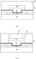
- specific steps of a method for manufacturing a semiconductor structure include: As shown in FIG. 4 , a first protective layer 80 is formed on the metal pad 10, and a second protective layer 90 is formed on the upper surface of the first protective layer 80 and the metal pad 10 using a deposition process. An opening is formed in the protective layer 90 where the bump 30 is pre-prepared by a photolithography process, and a metal material is deposited on the metal pad 10 and the second protective layer 90 to form an under-bump metal layer 70, wherein the under-bump metal layer 70 covers all the second protective layers 90 and the opening of the second protective layer 90.
- the material of the first protective layer 80 may be one or a combination of silicon dioxide and silicon nitride, and the material of the second protective layer 90 may be polyimide.
- the metal material layer of the under-bump metal layer 70 may include a Ti layer, a TiW layer, and a Cu layer.
- the under-bump metal layer 70 is formed on the metal pad 10 and the second protective layer 90 by means of physical vapor deposition (PVD).
- PVD physical vapor deposition
- the Ti layer of the under-bump metal layer 70 can be used to adhere and prevent the metal copper from diffusing into the semiconductor substrate 20 and the metal pad 10.
- the Cu layer of the under-bump metal layer 70 can be used to form the electrode of electroplated copper pillar (bump 30).
- the first photoresist layer 11 is formed on the second protective layer 90 at a part except the position corresponding to the bump 30 and the first solder layer 40, that is, leave a space in the middle of the first photoresist layer 11 preset for forming the bump 30 and the first solder layer 40, then the bump 30 and the first solder layer 40 are electroplated.
- the first photoresist layer 11 may be a photoresist layer. After the photoresist layer is coated, it is exposed and developed to form a space for arranging the bump 30 and the first solder layer 40.
- the material of the first solder layer 40 may be one of lead, tin, and silver or an alloy containing any one of the foregoing solder metals.
- the material of the first solder layer 40 may be an alloy with a tin content of 91.5% to 98.5% and a silver content of 8.5% to 1.5%.
- the material of the first solder layer 40 may be an alloy with a tin content of 93.2% to 96.5% and a silver content of 6.8% to 3.5%, and the material of the first solder layer 40 may be an alloy with a tin content of 98.2% to 98.5%,and a silver content of 1.8%-1.5%
- bump 30 is copper pillar.
- the first photoresist layer 11 is removed after the electroplated bump 30 and the first solder layer 40 are formed.
- a first mask layer 12 is formed on the semiconductor substrate 20 on which the first solder layer 40 is formed.
- the first mask layer 12 covers the first solder layer 40 and the under-bump metal layer 70.
- the first mask layer 12 may be a polyimide layer.
- the first mask layer 12 is lithographically used to expose part of the top surface of the first solder layer 40.
- a part of the first solder layer 40 is etched by chemical acid etching to form are moval space 41.
- the first mask layer 12 is removed.
- a second mask layer 13 is formed.
- the second mask layer 13 covers the first solder layer 40 and the under-bump metal layer 70.
- the second mask layer 13 is lithographically used to expose the first solder layer 40.
- the barrier layer 50 is deposited on the second mask layer 13 and the first solder layer 40 by using a physical vapor deposition (PVD) technology.
- PVD physical vapor deposition
- the barrier layer 50 may be a nickel layer, and when the barrier layer 50 needs to be thickened, an electroplating process may be applied to increase the thickness of the nickel layer.
- the second mask layer 13 may be a polyimide layer.
- a second photoresist layer 14 is formed on the barrier layer 50 at a position corresponding to the first solder layer 40.
- the second photoresist layer 14 covers the upper part of the first solder layer 40 and serves as a mask for the photolithography of the barrier layer 50, and the second photoresist layer 14 may be a photoresist layer.
- the metal material of the barrier layer 50 is etched at a position not covered by the second photoresist layer 14.
- the second photoresist layer 14 is removed to expose the first groove 51 on the barrier layer 50.
- solder is filled in the first groove 51 to form a second solder layer 60, and the top surface of the second solder layer 60 is higher than the barrier layer 50.
- the material of the second solder layer 60 may be one of lead, tin and silver or an alloy containing any one of the foregoing solder metals.
- the material of the second solder layer 60 may be an alloy with a tin content of 91.5% to 98.5% and a silver content of 8.5% to 1.5%.
- the material of the second solder layer 60 may be an alloy with a tin content of 93.2% to 96.5% and a silver content of 6.8% to 3.5%, and the material of the second solder layer 60 may be an alloy with a tin content of 98.2% to 98.5%, and a silver content of 1.8% to 1.5%.
- the second mask layer 13 is etched.
- the under-bump metal layer 70 is etched, and finally a high-temperature reflow process is applied to form a solder bump on the surface of the barrier layer 50, that is, the semiconductor structure shown in FIG. 1 is completed.
- the barrier layer 50 is deposited on the second mask layer 13 and the first solder layer 40 by using the physical vapor deposition (PVD) technology.
- PVD physical vapor deposition
- a third photoresist layer is formed on the metal material of the barrier layer 50 except the position corresponding to the first solder layer 40.
- the third patterning layer may be a photoresist layer.
- a second solder layer 60 is formed by filling solder in the first groove 51, and the top surface of the second solder layer 60 is higher than the barrier layer 50 but lower than the third photoresist layer.
- the material of the solder layer may be one of lead, tin, and silver or an alloy containing any one of the foregoing solder metals.
- the material of the second solder layer 60 may be an alloy with a tin content of 91.5% to 98.5% and a silver content of 8.5% to 1.5%.
- the material of the second solder layer 60 may be an alloy with a tin content of 93.2% to 96.5% and a silver content of 6.8% to 3.5%, and the material of the second solder layer 60 may be an alloy with a tin content of 98.2% to 98.5%, and a silver content of 1.8% to 1.5%.
- the second mask layer 13 is etched. Then, the under-bump metal layer 70 is etched, and finally a high-temperature reflow process is applied to form a solder bump on the surface of the barrier layer 50, that is, the semiconductor structure shown in FIG. 1 is completed.
- the barrier layer 50 may be a metal barrier layer.
Landscapes
- Internal Circuitry In Semiconductor Integrated Circuit Devices (AREA)
- Chemical & Material Sciences (AREA)
- Chemical Kinetics & Catalysis (AREA)
- General Chemical & Material Sciences (AREA)
Abstract
Description
- This disclosure claims priority to
Chinese Patent Application No.201911205447.1 filed on November 29, 2019 - The present disclosure relates to the field of semiconductor technology, and in particular to a semiconductor structure and a manufacturing method thereof.
- As integration levels, functions, and performance of integrated circuits become ever higher, plus the emergence of new types of integrated circuits, packaging technology has been playing an increasingly important role in the value of the entire integrated circuit products and it accounts for an increasing proportion of the value of the entire electronic systems. Bump interconnect technology, with its good electrical performance and resistance to electromigration, has become a key technology for the next generation chip interconnection at narrow-pitch.
- In the current arts, during the flip-chip soldering process, the packaging substrates tend to be warped when they are heated, the flatness difference between a chip and its substrate will occur, solder can creep if the amount of solder is not enough to weld, causing the problem of surface non-wetting, or solder bridging between blocks can occur if there is too much solder.
- Based on the above, it is necessary to provide a semiconductor structure and a manufacturing method to overcome the above-mentioned drawbacks in the prior art.
- According to the first embodiment of the present disclosure, there is provided a semiconductor structure, comprising: a semiconductor substrate; a metal pad, disposed on the semiconductor substrate; a bump, disposed on the metal pad; a barrier layer, disposed on a side of the bump away from the metal pad, the barrier layer includes a first surface and a second surface; a first solder layer, disposed between the bump and the first surface of the barrier layer; and a second solder layer, disposed on the second surface of the barrier layer.
- In some examples, the barrier layer comprises a first groove, a notch of the first groove faces a direction away from the first solder layer, and the second solder layer is disposed in the first groove, part of the second solder layer protrudes from the first groove; and/or the barrier layer further comprises a second groove, and the first solder layer is disposed in the second groove.
- In some examples, a cross section of the barrier layer has an H-shape.
- In some examples, the barrier layer and the bump are spaced apart and the first solder layer is provided between the barrier layer and the bump.
- In some examples, the second solder layer is provided in the first groove, and/or the first solder layer is provided in the second groove.
- In some examples, the first groove and the second groove are both semi-closed grooves.
- In some examples, a distance between a bottom surface of the second groove and a top surface of the bump is in a range of 5um to50um.
- In some examples, a depth of the first groove is greater than a depth of the second groove.
- In some examples, the bump comprises a copper pillar, the semiconductor structure further comprises: an under-bump metal layer, at least part of the under-bump metal layer is sandwiched between the metal pad and the bump.
- In some examples, the semiconductor structure further comprises: a first protection layer, disposed on the semiconductor substrate, the first protection layer comprises a first opening, and the first opening exposes part of the metal pad.
- In some examples, the semiconductor structure further comprises: a second protective layer, disposed on the first protective layer, the second protective layer comprises a second opening, a diameter of the second opening is smaller than or equal to a diameter of the first opening; and wherein the under-bump metal layer at least covers a bottom surface and sidewall surfaces of the second opening, and at least part of the under-bump metal layer is disposed in the second opening.
- According to another embodiment of the present disclosure, a method of manufacturing a semiconductor structure, comprising: providing a semiconductor substrate, and forming a metal pad on the semiconductor substrate; forming a bump on the metal pad; forming a first solder layer on a side of the bump away from the metal pad; forming a barrier layer on a side of the first solder layer away from the bump; and forming a second solder layer on a side of the barrier layer away from the first solder layer.
- In some examples, the barrier layer comprises a first groove and a second groove separated from each other, a notch of the first groove faces a direction away from the first solder layer, the first solder layer is arranged in the second groove, the second solder layer is formed in the first groove, and part of the second solder layer protrudes from the notch of the first groove.
- In some examples, before forming the bump, the manufacturing method further comprises: forming an under-bump metal layer on the metal pad, wherein at least part of the under-bump metal layer is sandwiched between the metal pad and the bump.
- In some examples, before forming the bump, the manufacturing method further comprises: forming a first protective layer on the semiconductor substrate, wherein the first protection layer has a first opening, and the first opening exposes part of the metal pad.
- In some examples, after forming the first protective layer, the manufacturing method further comprises: forming a second protective layer on an upper surface of the first protective layer and an upper surface of the metal pad; after forming the second protection layer, forming the under-bump metal layer on the metal pad and the second protection layer; wherein the second protection layer comprises a second opening, a diameter of the second opening is smaller than or equal to a diameter of the first opening; and the under-bump metal layer at least covers a bottom surface and sidewall surfaces of the second opening and at least part of the under-bump metal layer is disposed in the second opening.
- In some examples, before forming the bump, the manufacturing method further comprises: forming a first photoresist layer on the semiconductor substrate except positions corresponding to the bump and the first solder layer; and removing the first photoresist layer after forming the bump and the first solder layer.
- In some examples, before forming the barrier layer, the manufacturing method further comprises: forming a first mask layer on the semiconductor substrate on which the first solder layer is formed; photoetching the first mask layer by a photolithography process to expose part of the first solder layer; etching the part of the first solder layer by a chemical acid etching process, and then removing the first mask layer; forming a second mask layer; photoetching the second mask layer by a photolithography process to expose the first solder layer, the barrier layer is formed on the first solder layer and the second mask layer, wherein the first solder layer is arranged between the barrier layer and the bump.
- In some examples, after forming the barrier layer, the manufacturing method further comprises: forming a second photoresist layer on the barrier layer at a position corresponding to the first solder layer; etching the barrier layer at a position not covered by the second photoresist layer; removing the second photoresist layer; filling solder in the first groove to form the second solder layer; and removing the second mask layer.
- In some examples, after forming the barrier layer, the manufacturing method further comprises: forming a third photoresist layer on the barrier layer except a position corresponding to the first solder layer; filling solder in the first groove to form the second solder layer; removing the third photoresist layer; etching the barrier layer at a position not covered by solder; and removing the second mask layer.
- The semiconductor structure of the present disclosure includes a semiconductor substrate, a metal pad, a bump, a first solder layer, a barrier layer, and a second solder layer. The metal pad is disposed on the upper surface of the semiconductor substrate, and then the bump, the first solder layer, a barrier layer, and a second solder layer are sequentially disposed upwards. Since the second solder layer and the first solder layer are respectively arranged on two sides of the barrier layer, the problem of non-wetting caused by insufficient solder amount during the flip-chip soldering process can be mitigated.
- By considering the following detailed description of the preferred embodiments of the present disclosure in conjunction with the accompanying drawings, various objectives, features, and advantages of the present disclosure will become more apparent. The drawings are merely exemplary illustrations of the present disclosure and are not necessarily drawn to scale. In the drawings, the same reference numerals always indicate the same or similar parts. The figures are:
-
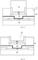
FIG. 1 is a schematic structural diagram showing a semiconductor structure according to an exemplary embodiment; -
FIG. 2 is a schematic structural diagram showing a semiconductor structure according to another exemplary embodiment; -
FIG. 3 is a schematic diagram showing an assembly structure of a semiconductor structure and a packaging substrate according to an exemplary embodiment; -
FIG. 4 is a schematic diagram showing a structure after forming an under-bump metal layer by a method formanufacturing a semiconductor structure according to an exemplary embodiment; -
FIG. 5 is a schematic diagram showing a structure after forming a first solder layer by a method for manufacturing a semiconductor structure according to an exemplary embodiment; -
FIG. 6 is a schematic diagram showing a structure after removing the first photoresist layer by a method for manufacturing a semiconductor structure according to an exemplary embodiment; -
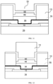
FIG. 7 is a schematic diagram showing a structure after forming a first mask layer by a method for manufacturing a semiconductor structure according to an exemplary embodiment; -
FIG. 8 is a schematic diagram showing a structure after lithography of a first mask layer by a method for manufacturing a semiconductor structure according to an exemplary embodiment; -
FIG. 9 is a schematic diagram showing a structure after acid etching the first mask layer by a method for manufacturing a semiconductor structure according to an exemplary embodiment; -
FIG. 10 is a schematic diagram showing a structure after removing the first mask layer by a method formanufacturing a semiconductor structure according to an exemplary embodiment; -
FIG. 11 is a schematic diagram showing a structure after forming a barrier layer by a method for manufacturing a semiconductor structure according to an exemplary embodiment; -
FIG. 12 is a schematic diagram showing a structure after forming a second photoresist layer by a method formanufacturing a semiconductor structure according to an exemplary embodiment; -
FIG. 13 is a schematic diagram showing a structure after etching the barrier layer by a method formanufacturing a semiconductor structure according to an exemplary embodiment; -
FIG. 14 is a schematic diagram showing a structure after removing a second photoresist layer by a method formanufacturing a semiconductor structure according to an exemplary embodiment; -
FIG. 15 is a schematic diagram showing a structure after forming a second solder layer by a method formanufacturing a semiconductor structure according to an exemplary embodiment; and -
FIG. 16 is a schematic diagram showing a structure after etching a second mask layer by a method for manufacturing a semiconductor structure according to an exemplary embodiment. - The reference numerals are explained as follows:
1. package substrate; 10, metal pad; 11, first photoresist layer; 12, first mask layer; 13, second mask layer; 14, second photoresist layer; 20, semiconductor substrate; 30, bump; 40, first solder layer; 41, removal space; 50, barrier layer; 51, first groove; 52, second groove; 60, second solder layer; 70, metal layer under-bump; 80, the first protective layer; 90, the second protective layer. - Typical embodiments showing the features and advantages of the present disclosure are described in detail in the following description.It should be understood that the present disclosure can have variouschanges in different embodiments without departing from the scope of the present disclosure. The description and drawings are essentially for illustrative purposes, rather than limiting the present disclosure.
- In the following description of the different exemplary embodiments of the present disclosure, reference is made to the accompanying drawings, which form a part of the present disclosure, and therein are shown by way of different exemplary structures, systems, and steps that can implement various aspects of the present disclosure. It should be understood that other specific solutions of components, structures, exemplary devices, systems, and steps can be used, and structural and functional modifications can be made without departing from the scope of the present disclosure. Moreover, although the terms "above", "between", "within", etc. may be used in this specification to describe different exemplary features and elements of the present disclosure, these terms are used herein for convenience only, such as according to the directions of the examples in a drawing. Nothing in this specification should be understood as requiring a specific three-dimensional direction of the structure to fall within the scope of the present disclosure.
- An embodiment of the present disclosure provides a semiconductor structure. Please refer to
FIG. 1 and FIG. 2 . The semiconductor structure includes: asemiconductor substrate 20; ametal pad 10 disposed on thesemiconductor substrate 20; abump 30 disposed on themetal pad 10; abarrier layer 50 is disposed at the side of thebump 30 away from themetal pad 10, thebarrier layer 50 includes a first surface facing down and a second surface facing up; thefirst solder layer 40 is disposed between thebump 30 and the first surface of thebarrier layer 50; and thesecond solder layer 60 is disposed on the second surface of thebarrier layer 50. - The semiconductor structure of an embodiment of the present disclosure is composed of a
semiconductor substrate 20, ametal pad 10, abump 30, afirst solder layer 40, abarrier layer 50, and asecond solder layer 60. Themetal pad 10 is disposed onan upper surface of thesemiconductor substrate 20. The surface is then provided with abump 30, afirst solder layer 40, abarrier layer 50, and asecond solder layer 60 in an upwards order. Since thesecond solder layer 60 and thefirst solder layer 40 are respectively disposed on two sides of thebarrier layer 50, the problem of surface non-wetting caused by insufficient solder amount during the flip-chip soldering process can be mitigated. - In one embodiment, the
barrier layer 50 has afirst groove 51, the notch of thefirst groove 51 faces away from thefirst solder layer 40, thesecond solder layer 60 is disposed in thefirst groove 51, and part of thesecond solder layer 60 protrudes from the notch of thefirst groove 51; and/or thebarrier layer 50 has asecond groove 52, and thefirst solder layer 40 is disposed in thesecond groove 52, the first surface of the barrier layer is the bottom surface of thesecond groove 52, and the second surface of the barrier layer is the bottom surface of thefirst groove 51. From the arrangement of thefirst groove 51 and/or thesecond groove 52, during the flip-chip reflow process, thebarrier layer 50 can block the flow of the solder and play a role of drainage. - In one embodiment, referring to
FIG. 1 and FIG. 2 , the semiconductor structure includes: asemiconductor substrate 20; ametal pad 10 arranged on thesemiconductor substrate 20; abump 30 arranged on themetal pad 10; afirst solder layer 40, arranged on the side of thebump 30 away from themetal pad 10; thebarrier layer 50 is arranged on the side of thefirst solder layer 40 away from thebump 30, thebarrier layer 50 has afirst groove 51 and asecond groove 52, the notch of thefirst groove 51 faces away from thefirst solder layer 40, thefirst solder layer 40 is arranged in thesecond groove 52; thesecond solder layer 60 is arranged in thefirst groove 51, part of thesecond solder layer 60 protrudes from the notch of thefirst groove 51. - The semiconductor structure of an embodiment of the present disclosure is composed of a
semiconductor substrate 20, ametal pad 10, abump 30, afirst solder layer 40, abarrier layer 50, and asecond solder layer 60. Themetal pad 10 is disposed on an upper surface of thesemiconductor substrate 20. The surface of themetal pad 10 is then provided with abump 30, afirst solder layer 40, abarrier layer 50, and asecond solder layer 60 in an upward order. Since thesecond solder layer 60 and thefirst solder layer 40 are tucked in thebarrier layer 50, the non-wetting problem caused by insufficient solder and solder bridging caused by excessive solder volume are both improved during the flip-chip soldering process. - In one embodiment, as shown in
FIG. 3 , the semiconductor structure is a stretchable metal. During the flip-chip soldering process, thepackage substrate 1 is heated and warped, and thefirst solder layer 40 has gone through reflow at a high temperature, melted and stretchable. Therefore, the height adjustment is automatically performed, which can reduce the non-wetting problem caused by the deformation of thepackage substrate 1 after reflow. - In one embodiment, the
first groove 51 and thesecond groove 52 of thebarrier layer 50 each have only one opening, that is, thefirst groove 51 and thesecond groove 52 are both semi-closed grooves. During the flip-chip reflow process, thebarrier layer 50 can block the flow of the solder and play a role of drainage, so that thesecond solder layer 60 does not diffuse in large amounts, which avoids the problem of solder bridging, meeting the goal of improving the yield. - In one embodiment, the distance between the bottom surface of the
second groove 52 and the top surface of thebump 30 is 5um-50um, that is, the thickness of thefirst solder layer 40 between the bottom surface of thesecond groove 52 and the top surface of thebump 30 ranges from 5um to 50um. Further, the distance between the bottom surface of thesecond groove 52 and the top surface of thebump 30 is 15um-35um. Optionally, the distance between the bottom surface of thesecond groove 52 and the top surface of thebump 30 is about 5um, 10 um, 13 um, 15um, 20 um, 30 um, 35um, 40 um, 42 um or 50um. - In one embodiment, the depth of the
first groove 51 is greater than the depth of thesecond groove 52, that is, the thickness of thesecond solder layer 60 located in thefirst groove 51 is greater than the thickness of thesolder layer 40 located in thefirst groove 51. - In one embodiment, the material of the
first solder layer 40 and thesecond solder layer 60 may include one of lead, tin, and silver and an alloy containing any one of the foregoing solder metals. For example, the material of thefirst solder layer 40 and/or thesecond solder layer 60 may be an alloy with a tin content of 91.5% to 98.5% and a silver content of 8.5% to 1.5%. Optionally, the material of thefirst solder layer 40 and/or thesecond solder layer 60 may be an alloy with a tin content of 93.2% to 96.5% and a silver content of 6.8% to 3.5%, the material of thefirst solder layer 40, and/ or thesecond solder layer 60 may be an alloy with a tin content of 98.2% to 98.5% and a silver content of 1.8% to 1.5%. - In one embodiment, the
semiconductor base 20 includes a semiconductor substrate and a number of IC circuits and insulating layers. The material of themetal pad 10 may be aluminum or copper, but is not limited thereto. - In one embodiment, the cross section of the
barrier layer 50 is H-shaped. The cross section of thebarrier layer 50 can be understood as a longitudinal cross section of thebarrier layer 50 with reference toFIG. 1 and FIG. 2 . Thebarrier layer 50 is a barrel-shaped structure with a separator in the middle, and thesecond solder layer 60 and thefirst solder layer 40 are not in direct contact with each other. - In one embodiment, the
barrier layer 50 and thebump 30 are spaced apart, and afirst solder layer 40 is provided between thebarrier layer 50 and thebump 30. Thefirst solder layer 40 has a reversed T-shaped cross section, that is, the smaller end of thefirst solder layer 40 is located in thesecond groove 52, and the larger end of thefirst solder layer 40 is located beyond thesecond groove 52. - In one embodiment, the
second solder layer 60 is provided in thefirst groove 51, and/or thefirst solder layer 40 is provided in thesecond groove 52. Wherein, the portion of thesecond solder layer 60 protruding out from thefirst groove 51 may cover part of the upper surface of thebarrier layer 50 or fully cover the upper surface of thebarrier layer 50, however, it is possible that the upper surface of thebarrier layer 50 is not covered at all. - In an embodiment, the
barrier layer 50 is a metal barrier layer, and the material of thebarrier layer 50 may include nickel. - In one embodiment, the
bump 30 is a copper pillar, and the semiconductor structure further includes: an under-bump metal layer 70, at least part of the under-bump metal layer 70 is sandwiched between themetal pad 10 and thebump 30. The metal material of the under-bump metal layer 70 may include a titanium (Ti) layer, a titanium tungsten (TiW) layer, and a copper (Cu) layer. The under-bump metal layer 70 is electrically connected to themetal pad 10. The under-bump metal layer 70 prevents thebump 30 from directly contacting themetal pad 10. - In one embodiment, the semiconductor structure further includes: a
first protection layer 80 disposed on thesemiconductor substrate 20, thefirst protection layer 80 has a first opening, and the first opening exposes a portion of themetal pad 10, that is, thefirst protection layer 80 covers the peripheral outer edge of themetal pad 10. Wherein, the material of thefirst protection layer 80 may be one or a combination of silicon dioxide and silicon nitride. - In one embodiment, the first
protective layer 80 covers part of themetal pad 10 and thesemiconductor substrate 20 area outside themetal pad 10. - In one embodiment, the semiconductor structure further includes: a second
protective layer 90 disposed on the firstprotective layer 80, the secondprotective layer 90 has a second opening, and the diameter of the second opening is smaller than or equal to the diameter of the first opening in thefirst protection layer 80; wherein, the under-bump metal layer 70 covers at least the bottom surface and the sidewalls of the second opening of the second protective layer, and at least part of the under-bump metal layer 70 is disposed in the second opening. The material of the secondprotective layer 90 may be polyimide. - In one embodiment, the under-
bump metal layer 70 is disposed on a part of thesecond protection layer 90 and the exposedmetal pad 10. In one embodiment, the under-bump metal layer 70 may enclose thebump 30, that is, thebump 30 is located in the open cavity formed by the under-bump metal layer 70, and the plane of the notch of the under-bump metal layer 70 is in the same plane with the bottom surface of thefirst solder layer 40. - In one embodiment, as shown in
FIG. 1 , the semiconductor structure is composed of asemiconductor substrate 20, ametal pad 10, abump 30, afirst solder layer 40, abarrier layer 50, asecond solder layer 60, an under-bump metal layer 70, a firstprotective layer 80 and a secondprotective layer 90. The firstprotective layer 80 covers themetal pad 10, and shields part of themetal pad 10. The secondprotective layer 90 is disposed on the firstprotective layer 80 and covers part of themetal pad 10. The position where the secondprotective layer 90 and the firstprotective layer 80 cover themetal pad 10 are face each other, that is, thefirst protection layer 80 is located under thesecond protection layer 90. The secondprotective layer 90 does not cover the middle part of themetal pad 10. In the under-bump metal layer 70, metal material layers such as a Ti layer, a TiW layer, and a Cu layer are deposited on the bottom surface and sidewalls of the second opening of the secondprotective layer 90 over themetal pad 10 by the physical vapor deposition process. Here the Ti layer can be used to adhere and prevent the metal copper from diffusing into thesemiconductor substrate 20, and the Cu layercan be used to form electroplated electrodes. Thebump 30 has a T-shaped cross section, that is, the smaller end of thebump 30 is located in the under-bump metal layer 70 and the larger end of thebump 30 is located outside the under-bump metal layer 70. - In another embodiment, as shown in
FIG. 2 , the semiconductor structure is composed of asemiconductor substrate 20, ametal pad 10, abump 30, afirst solder layer 40, abarrier layer 50, asecond solder layer 60, an under-bump metal layer 70, and a firstprotective layer 80. The firstprotective layer 80 covers themetal pad 10 and shields part of themetal pad 10. In the under-bump metal layer 70, metal material layers such as a Ti layer, a TiW layer, and a Cu layer are disposed on themetal pad 10 by the physical vapor deposition process. The Ti layer can be used to adhere and prevent the metal copper from diffusing into thesemiconductor substrate 20. The Cu layer can be used to form electroplated electrodes. Thebump 30 has a rectangular cross section, and thebump 30 is located between the under-bump metal layer 70 and thefirst solder layer 40. - An embodiment of the present disclosure also provides a method for manufacturing a semiconductor structure, including: providing a
semiconductor substrate 20, and forming ametal pad 10 on thesemiconductor substrate 20; forming abump 30 on themetal pad 10; forming afirst solder layer 40 on the side of thebump 30 away from themetal pad 10; forming abarrier layer 50 on the side of thefirst solder layer 40 away from thebump 30; forming asecond solder layer 60 on the side of thebarrier layer 50 away from thefirst solder layer 40. - Specifically, the
barrier layer 50 has afirst groove 51 and asecond groove 52 that are separated from each other. The notch of thefirst groove 51 faces away from thefirst solder layer 40, and thefirst solder layer 40 is disposed in thesecond groove 52, asecond solder layer 60 is formed in thefirst groove 51, and part of thesecond solder layer 60 protrudes from the notch of thefirst groove 51. - In one embodiment, a method for manufacturing a semiconductor structure includes: providing a
semiconductor substrate 20 and forming ametal pad 10 on thesemiconductor substrate 20; forming abump 30 on themetal pad 10; afirst solder layer 40 is formed on the side of thebump 30 away from themetal pad 10; abarrier layer 50 is formed on the side of thefirst solder layer 40 away from thebump 30. Thebarrier layer 50 has afirst groove 51 and asecond groove 52 that are separated from each other. The notch of thegroove 51 faces away from thefirst solder layer 40, and thefirst solder layer 40 is disposed in thesecond groove 52; asecond solder layer 60 is formed in thefirst groove 51, and part of thesecond solder layer 60 protrudes from the notch of thefirst groove 51. - In one embodiment, before forming the
bump 30, the manufacturing method further includes: forming an under-bump metal layer 70 on themetal pad 10; wherein at least part of the under-bump metal layer 70 is sandwiched between themetal pad 10 and thebump 30. - In one embodiment, before forming the
bump 30, the manufacturing method further includes: forming a firstprotective layer 80 on thesemiconductor substrate 20; wherein the firstprotective layer 80 has a first opening, and the first opening exposes part of themetal pad 10. - In one embodiment, after forming the first
protective layer 80, the manufacturing method further includes: forming a secondprotective layer 90 on the upper surface of the firstprotective layer 80 and themetal pad 10; after forming the secondprotective layer 90, an under-bump metal layer 70 is formed on themetal pad 10 and thesecond protection layer 90; wherein thesecond protection layer 90 has a second opening, and the diameter of the second opening of the secondprotective layer 90 is smaller than or equal to the diameter of the first opening of the firstprotective layer 80. The under-bump metal layer 70 covers at least the bottom surface and the sidewalls of the second opening of thesecond protection layer 90, and at least part of the under-bump metal layer 70 is disposed in the second opening of thesecond protection layer 90. - In one embodiment, before forming the
bump 30, the manufacturing method further includes: forming thefirst photoresist layer 11 on thesemiconductor substrate 20 at a part except the position corresponding to thebump 30 and thefirst solder layer 40; after thebumps 30 and thefirst solder layer 40 are formed, thefirst photoresist layer 11 is removed. - In one embodiment, before forming the
barrier layer 50, the manufacturing method further includes: forming thefirst mask layer 12 on thesemiconductor substrate 20 on which thefirst solder layer 40 is formed; and using a photolithography process to photoetch thefirst mask layer 12 to expose part of thefirst solder layer 40; using a chemical acid etching process to etch part of thefirst solder layer 40, and then removing thefirst mask layer 12; forming thesecond mask layer 13; and using a photolithography process to photoetch thesecond mask layer 13 to expose thefirst solder layer 40, forming abarrier layer 50 on thefirst solder layer 40 and thesecond mask layer 13, wherein afirst solder layer 40 is provided between thebarrier layer 50 and thebump 30. - In one embodiment, after forming the
barrier layer 50, the manufacturing method further includes: forming asecond photoresist layer 14 on thebarrier layer 50 at a position corresponding to thefirst solder layer 40; etching thebarrier layer 50 at the positionnot covered by thesecond photoresist layer 14; removing thesecond photoresist layer 14; filling thefirst groove 51 with solder to form thesecond solder layer 60; removing thesecond mask layer 13. - In one embodiment, after forming the
barrier layer 50, the manufacturing method further includes: forming a third photoresist layer on thebarrier layer 50 except the position corresponding to thefirst solder layer 40; filling thefirst groove 51 with solder to form thesecond solder layer 60; removing the third photoresist layer; etching thebarrier layer 50 at the position not covered by the solder; and removing thesecond mask layer 13. - In an embodiment, specific steps of a method for manufacturing a semiconductor structure include:
As shown inFIG. 4 , a firstprotective layer 80 is formed on themetal pad 10, and a secondprotective layer 90 is formed on the upper surface of the firstprotective layer 80 and themetal pad 10 using a deposition process. An opening is formed in theprotective layer 90 where thebump 30 is pre-prepared by a photolithography process, and a metal material is deposited on themetal pad 10 and the secondprotective layer 90 to form an under-bump metal layer 70, wherein the under-bump metal layer 70 covers all the secondprotective layers 90 and the opening of the secondprotective layer 90. The material of the firstprotective layer 80 may be one or a combination of silicon dioxide and silicon nitride, and the material of the secondprotective layer 90 may be polyimide. The metal material layer of the under-bump metal layer 70 may include a Ti layer, a TiW layer, and a Cu layer. The under-bump metal layer 70 is formed on themetal pad 10 and the secondprotective layer 90 by means of physical vapor deposition (PVD). The Ti layer of the under-bump metal layer 70 can be used to adhere and prevent the metal copper from diffusing into thesemiconductor substrate 20 and themetal pad 10. The Cu layer of the under-bump metal layer 70 can be used to form the electrode of electroplated copper pillar (bump 30). - As shown in
FIG. 5 , thefirst photoresist layer 11 is formed on the secondprotective layer 90 at a part except the position corresponding to thebump 30 and thefirst solder layer 40, that is, leave a space in the middle of thefirst photoresist layer 11 preset for forming thebump 30 and thefirst solder layer 40, then thebump 30 and thefirst solder layer 40 are electroplated. Thefirst photoresist layer 11 may be a photoresist layer. After the photoresist layer is coated, it is exposed and developed to form a space for arranging thebump 30 and thefirst solder layer 40. The material of thefirst solder layer 40 may be one of lead, tin, and silver or an alloy containing any one of the foregoing solder metals. For example, the material of thefirst solder layer 40 may be an alloy with a tin content of 91.5% to 98.5% and a silver content of 8.5% to 1.5%. Optionally, the material of thefirst solder layer 40 may be an alloy with a tin content of 93.2% to 96.5% and a silver content of 6.8% to 3.5%, and the material of thefirst solder layer 40 may be an alloy with a tin content of 98.2% to 98.5%,and a silver content of 1.8%-1.5%,bump 30 is copper pillar. - As shown in
FIG. 6 , thefirst photoresist layer 11 is removed after the electroplatedbump 30 and thefirst solder layer 40 are formed. - As shown in
FIG. 7 , afirst mask layer 12 is formed on thesemiconductor substrate 20 on which thefirst solder layer 40 is formed. Thefirst mask layer 12 covers thefirst solder layer 40 and the under-bump metal layer 70. Where thefirst mask layer 12 may be a polyimide layer. - As shown in
FIG. 8 , thefirst mask layer 12 is lithographically used to expose part of the top surface of thefirst solder layer 40. - As shown in
FIG. 9 , a part of thefirst solder layer 40 is etched by chemical acid etching to form aremoval space 41. - As shown in
FIG. 10 , thefirst mask layer 12 is removed. - As shown in
FIG. 11 , asecond mask layer 13 is formed. Thesecond mask layer 13 covers thefirst solder layer 40 and the under-bump metal layer 70. Thesecond mask layer 13 is lithographically used to expose thefirst solder layer 40. Thebarrier layer 50 is deposited on thesecond mask layer 13 and thefirst solder layer 40 by using a physical vapor deposition (PVD) technology. Wherein, thebarrier layer 50 may be a nickel layer, and when thebarrier layer 50 needs to be thickened, an electroplating process may be applied to increase the thickness of the nickel layer. Wherein, thesecond mask layer 13 may be a polyimide layer. - As shown in
FIG. 12 , asecond photoresist layer 14 is formed on thebarrier layer 50 at a position corresponding to thefirst solder layer 40. Where thesecond photoresist layer 14 covers the upper part of thefirst solder layer 40 and serves as a mask for the photolithography of thebarrier layer 50, and thesecond photoresist layer 14 may be a photoresist layer. - As shown in
FIG. 13 , the metal material of thebarrier layer 50 is etched at a position not covered by thesecond photoresist layer 14. - As shown in
FIG. 14 , thesecond photoresist layer 14 is removed to expose thefirst groove 51 on thebarrier layer 50. - As shown in
FIG. 15 , solder is filled in thefirst groove 51 to form asecond solder layer 60, and the top surface of thesecond solder layer 60 is higher than thebarrier layer 50. Where the material of thesecond solder layer 60 may be one of lead, tin and silver or an alloy containing any one of the foregoing solder metals. For example, the material of thesecond solder layer 60 may be an alloy with a tin content of 91.5% to 98.5% and a silver content of 8.5% to 1.5%. Optionally, the material of thesecond solder layer 60 may be an alloy with a tin content of 93.2% to 96.5% and a silver content of 6.8% to 3.5%, and the material of thesecond solder layer 60 may be an alloy with a tin content of 98.2% to 98.5%, and a silver content of 1.8% to 1.5%. - As shown in
FIG. 16 , thesecond mask layer 13 is etched. Then, the under-bump metal layer 70 is etched, and finally a high-temperature reflow process is applied to form a solder bump on the surface of thebarrier layer 50, that is, the semiconductor structure shown inFIG. 1 is completed. - In another embodiment, specific steps of a method for manufacturing a semiconductor structure include the following.
- After the manufacturing process shown in
FIGS. 4 to 11 is completed, thebarrier layer 50 is deposited on thesecond mask layer 13 and thefirst solder layer 40 by using the physical vapor deposition (PVD) technology. - A third photoresist layer is formed on the metal material of the
barrier layer 50 except the position corresponding to thefirst solder layer 40. Where the third patterning layer may be a photoresist layer. - A
second solder layer 60 is formed by filling solder in thefirst groove 51, and the top surface of thesecond solder layer 60 is higher than thebarrier layer 50 but lower than the third photoresist layer. Where the material of the solder layer may be one of lead, tin, and silver or an alloy containing any one of the foregoing solder metals. For example, the material of thesecond solder layer 60 may be an alloy with a tin content of 91.5% to 98.5% and a silver content of 8.5% to 1.5%. Optionally, the material of thesecond solder layer 60 may be an alloy with a tin content of 93.2% to 96.5% and a silver content of 6.8% to 3.5%, and the material of thesecond solder layer 60 may be an alloy with a tin content of 98.2% to 98.5%, and a silver content of 1.8% to 1.5%. - Then the third photoresist layer is removed.
- The
second mask layer 13 is etched. Then, the under-bump metal layer 70 is etched, and finally a high-temperature reflow process is applied to form a solder bump on the surface of thebarrier layer 50, that is, the semiconductor structure shown inFIG. 1 is completed. - It should be noted that the
barrier layer 50 may be a metal barrier layer. - Those skilled in the art will easily think of other embodiments of the present disclosure after considering the description and practicing the invention disclosed herein. The present disclosure is intended to cover any variations, uses or adaptive changes of the present disclosure. These variations, uses or adaptive changes follow the general principles of the present disclosure and include common knowledge or conventional technical means in the technical field not disclosed by the present disclosure. The specification and example embodiments are to be regarded as exemplary only, and the true scope and spirit of the present disclosure are pointed out by the following claims.
- It should be understood that the present disclosure is not limited to the precise structure described above and shown in the drawings, and various modifications and changes can be made without departing from its scope. The scope of the present disclosure is only limited by the appended claims.
Claims (20)
- A semiconductor structure, comprising:a semiconductor substrate;a metal pad, disposed on the semiconductor substrate;a bump, disposed on the metal pad;a barrier layer, disposed on a side of the bump away from the metal pad, the barrier layer includes a first surface and a second surface;a first solder layer, disposed between the bump and the first surface of the barrier layer; anda second solder layer, disposed on the second surface of the barrier layer.
- The semiconductor structure of claim 1, wherein the barrier layer comprises a first groove, a notch of the first groove faces a direction away from the first solder layer, and the second solder layer is disposed in the first groove, part of the second solder layer protrudes from the first groove;
and/or, wherein the barrier layer further comprises a second groove, and the first solder layer is disposed in the second groove. - The semiconductor structure of claim 2, wherein a cross section of the barrier layer has an H-shape.
- The semiconductor structure of claim 2, wherein the barrier layer and the bump are spaced apart, and the first solder layer is provided between the barrier layer and the bump.
- The semiconductor structure of claim 2, wherein the second solder layer is provided in the first groove, and/or the first solder layer is provided in the second groove.
- The semiconductor structure of claim 2, wherein the firstgroove and the second groove are both semi-closed grooves.
- The semiconductor structure of claim 2, wherein a distance between a bottom surface of the second groove and a top surface of the bump is in a range of 5um to 50um.
- The semiconductor structure of claim 2, wherein a depth of the first groove is greater than a depth of the second groove.
- The semiconductor structure according to any one of claims 1 to 8, the bump comprises a copper pillar, the semiconductor structure further comprises: an under-bump metal layer, at least part of the under-bump metal layer is sandwiched between the metal pad and the bump.
- The semiconductor structure of claim 9, the semiconductor structure further comprises:
a first protection layer, disposed on the semiconductor substrate, the first protection layer comprises a first opening, and the first opening exposes part of the metal pad. - The semiconductor structure of claim 10, the semiconductor structure further comprises:a second protective layer, disposed on the first protective layer, the second protective layer comprises a second opening, a diameter of the second opening is smaller than or equal to a diameter of the first opening;wherein the under-bump metal layer at least covers a bottom surface and sidewall surfaces of the second opening, and at least part of the under-bump metal layer is disposed in the second opening.
- A method of manufacturing a semiconductor structure, comprising:providing a semiconductor substrate, and forming a metal pad on the semiconductor substrate;forming a bump on the metal pad;forming a first solder layer on a side of the bump away from the metal pad;forming a barrier layer on a side of the first solder layer away from the bump; andforming a second solder layer on a side of the barrier layer away from the first solder layer.
- The manufacturing method of claim 12, wherein the barrier layer comprises a first groove and a second groove separated from each other, a notch of the first groove faces a direction away from the first solder layer, the first solder layer is arranged in the second groove, the second solder layer is formed in the first groove, and part of the second solder layer protrudes from the notch of the first groove.
- The manufacturing method of claim 13, before forming the bump, the manufacturing method further comprises: forming an under-bump metal layer on the metal pad, wherein at least part of the under-bump metal layer is sandwiched between the metal pad and the bump.
- The manufacturing method of claim 14, before forming the bump, the manufacturing method further comprises:
forming a first protective layer on the semiconductor substrate, wherein the first protection layer has a first opening, and the first opening exposes part of the metal pad. - The manufacturing method of claim 15, after forming the first protective layer, the manufacturing method further comprises:forming a second protective layer on an upper surface of the first protective layer and an upper surface of the metal pad;after forming the second protection layer, forming the under-bump metal layer on the metal pad and the second protection layer;wherein the second protection layer comprises a second opening, a diameter of the second opening is smaller than or equal to a diameter of the first opening; andthe under-bump metal layer at least covers a bottom surface and sidewall surfaces of the second opening and at least part of the under-bump metal layer is disposed in the second opening.
- The manufacturing method of claims 13 to 16, before forming the bump, the manufacturing method further comprises:forming a first photoresist layer on the semiconductor substrate except positions corresponding to the bump and the first solder layer; andremoving the first photoresist layer after forming the bump and the first solder layer.
- The manufacturing method of claims 13 to 16, before forming the barrier layer, the manufacturing method further comprises:forming a first mask layer on the semiconductor substrate on which the first solder layer is formed;photoetching the first mask layer by a photolithography process to expose part of the first solder layer;etching the part of the first solder layer by a chemical acid etching process, and then removing the first mask layer;forming a second mask layer; andphotoetching the second mask layer by a photolithography process to expose the first solder layer, the barrier layer is formed on the first solder layer and the second mask layer, wherein the first solder layer is arranged between the barrier layer and the bump.
- The manufacturing method of claim 18, after forming the barrier layer, the manufacturing method further comprises:forming a second photoresist layer on the barrier layer at a position corresponding to the first solder layer;etching the barrier layerat a position not covered by the second photoresist layer;removing the second photoresist layer;filling solder in the first groove to form the second solder layer; andremoving the second mask layer.
- The manufacturing method of claim 18, after forming the barrier layer, the manufacturing method further comprises:forming a third photoresist layer on the barrier layer except a position corresponding to the first solder layer;filling solder in the first groove to form the second solder layer;removing the third photoresist layer;etching the barrier layer at a position not covered by solder; andremoving the second mask layer.
Applications Claiming Priority (2)
| Application Number | Priority Date | Filing Date | Title |
|---|---|---|---|
| CN201911205447.1A CN112885802A (en) | 2019-11-29 | 2019-11-29 | Semiconductor structure and manufacturing method thereof |
| PCT/CN2020/096085 WO2021103489A1 (en) | 2019-11-29 | 2020-06-15 | Semiconductor structure and manufacturing method therefor |
Publications (3)
| Publication Number | Publication Date |
|---|---|
| EP3940772A1 true EP3940772A1 (en) | 2022-01-19 |
| EP3940772A4 EP3940772A4 (en) | 2022-07-13 |
| EP3940772B1 EP3940772B1 (en) | 2024-07-17 |
Family
ID=76039658
Family Applications (1)
| Application Number | Title | Priority Date | Filing Date |
|---|---|---|---|
| EP20893357.2A Active EP3940772B1 (en) | 2019-11-29 | 2020-06-15 | Semiconductor structure and manufacturing method therefor |
Country Status (4)
| Country | Link |
|---|---|
| US (1) | US11855032B2 (en) |
| EP (1) | EP3940772B1 (en) |
| CN (1) | CN112885802A (en) |
| WO (1) | WO2021103489A1 (en) |
Families Citing this family (2)
| Publication number | Priority date | Publication date | Assignee | Title |
|---|---|---|---|---|
| CN112885802A (en) | 2019-11-29 | 2021-06-01 | 长鑫存储技术有限公司 | Semiconductor structure and manufacturing method thereof |
| GB202217714D0 (en) * | 2022-11-25 | 2023-01-11 | Spts Technologies Ltd | Method of operating a pvd apparatus |
Family Cites Families (16)
| Publication number | Priority date | Publication date | Assignee | Title |
|---|---|---|---|---|
| US5130779A (en) * | 1990-06-19 | 1992-07-14 | International Business Machines Corporation | Solder mass having conductive encapsulating arrangement |
| AU2927897A (en) * | 1996-04-29 | 1997-11-19 | Carl Shine | Multilayer solder/barrier attach for semiconductor chip |
| US6281106B1 (en) * | 1999-11-25 | 2001-08-28 | Delphi Technologies, Inc. | Method of solder bumping a circuit component |
| JP2008109009A (en) * | 2006-10-27 | 2008-05-08 | Sony Corp | Manufacturing method of semiconductor device |
| US7786001B2 (en) * | 2007-04-11 | 2010-08-31 | International Business Machines Corporation | Electrical interconnect structure and method |
| EP2075834A1 (en) * | 2007-12-28 | 2009-07-01 | INTERUNIVERSITAIR MICROELEKTRONICA CENTRUM vzw (IMEC) | Solder bumps for flip chip bonding with higher density |
| US9087829B2 (en) | 2011-08-05 | 2015-07-21 | Infineon Technologies Ag | Semiconductor arrangement |
| JPWO2014033977A1 (en) * | 2012-08-29 | 2016-08-08 | パナソニックIpマネジメント株式会社 | Semiconductor device |
| CN102915978B (en) * | 2012-11-08 | 2016-02-03 | 南通富士通微电子股份有限公司 | Semiconductor package |
| US9355980B2 (en) * | 2013-09-03 | 2016-05-31 | Taiwan Semiconductor Manufacturing Company, Ltd. | Three-dimensional chip stack and method of forming the same |
| US10276539B1 (en) * | 2017-10-30 | 2019-04-30 | Micron Technology, Inc. | Method for 3D ink jet TCB interconnect control |
| US10483221B2 (en) * | 2017-10-30 | 2019-11-19 | Micron Technology, Inc. | 3DI solder cup |
| CN209119091U (en) * | 2018-11-20 | 2019-07-16 | 长鑫存储技术有限公司 | Copper pillar bump structure |
| CN209045542U (en) * | 2018-11-30 | 2019-06-28 | 长鑫存储技术有限公司 | Semiconductor devices |
| CN210640233U (en) * | 2019-11-29 | 2020-05-29 | 长鑫存储技术有限公司 | Semiconductor structure |
| CN112885802A (en) | 2019-11-29 | 2021-06-01 | 长鑫存储技术有限公司 | Semiconductor structure and manufacturing method thereof |
-
2019
- 2019-11-29 CN CN201911205447.1A patent/CN112885802A/en active Pending
-
2020
- 2020-06-15 US US17/429,592 patent/US11855032B2/en active Active
- 2020-06-15 EP EP20893357.2A patent/EP3940772B1/en active Active
- 2020-06-15 WO PCT/CN2020/096085 patent/WO2021103489A1/en not_active Ceased
Also Published As
| Publication number | Publication date |
|---|---|
| CN112885802A (en) | 2021-06-01 |
| EP3940772B1 (en) | 2024-07-17 |
| EP3940772A4 (en) | 2022-07-13 |
| US11855032B2 (en) | 2023-12-26 |
| WO2021103489A1 (en) | 2021-06-03 |
| US20220115352A1 (en) | 2022-04-14 |
Similar Documents
| Publication | Publication Date | Title |
|---|---|---|
| CN100555616C (en) | Electronic component, semiconductor device using same, and method of manufacturing electronic component | |
| US7638421B2 (en) | Manufacturing method for semiconductor device and semiconductor device | |
| US9391036B2 (en) | Semiconductor device and manufacturing method thereof | |
| US11798885B2 (en) | Method of fabricating copper pillar bump structure with solder supporting barrier | |
| US20040060970A1 (en) | Under bump metallurgy for Lead-Tin bump over copper pad | |
| KR102578794B1 (en) | Semiconductor device and method for manufacturing the same | |
| JP5064632B2 (en) | Method and apparatus for forming an interconnect structure | |
| CN111199946A (en) | Copper pillar bump structure and manufacturing method thereof | |
| US20250357145A1 (en) | Bump structure and method of making the same | |
| US9059004B2 (en) | Method for chip scale package and package structure thereof | |
| EP3940772B1 (en) | Semiconductor structure and manufacturing method therefor | |
| CN209119091U (en) | Copper pillar bump structure | |
| CN210640231U (en) | semiconductor structure | |
| US11876064B2 (en) | Semiconductor structure and manufacturing method thereof | |
| CN210640233U (en) | Semiconductor structure | |
| CN210640230U (en) | Semiconductor structure | |
| US12336339B2 (en) | Micro light emitting diode structure and micro light emitting diode display device | |
| US11417539B2 (en) | Bump structure and method of making the same | |
| KR20020060307A (en) | Manufacturing method for solder bump | |
| JP2009135345A (en) | Semiconductor device and manufacturing method thereof | |
| JP2000040715A (en) | Flip chip mounted semiconductor device and method of manufacturing flip chip mounted semiconductor device | |
| CN112885801A (en) | Semiconductor structure and manufacturing method thereof | |
| KR100597994B1 (en) | Solder bump of semiconductor package and manufacturing method thereof | |
| KR20020071096A (en) | Method of forming solder bumps |
Legal Events
| Date | Code | Title | Description |
|---|---|---|---|
| STAA | Information on the status of an ep patent application or granted ep patent |
Free format text: STATUS: THE INTERNATIONAL PUBLICATION HAS BEEN MADE |
|
| PUAI | Public reference made under article 153(3) epc to a published international application that has entered the european phase |
Free format text: ORIGINAL CODE: 0009012 |
|
| STAA | Information on the status of an ep patent application or granted ep patent |
Free format text: STATUS: REQUEST FOR EXAMINATION WAS MADE |
|
| 17P | Request for examination filed |
Effective date: 20211015 |
|
| AK | Designated contracting states |
Kind code of ref document: A1 Designated state(s): AL AT BE BG CH CY CZ DE DK EE ES FI FR GB GR HR HU IE IS IT LI LT LU LV MC MK MT NL NO PL PT RO RS SE SI SK SM TR |
|
| A4 | Supplementary search report drawn up and despatched |
Effective date: 20220615 |
|
| RIC1 | Information provided on ipc code assigned before grant |
Ipc: H01L 23/31 20060101ALN20220610BHEP Ipc: H01L 23/00 20060101ALI20220610BHEP Ipc: H01L 23/488 20060101AFI20220610BHEP |
|
| STAA | Information on the status of an ep patent application or granted ep patent |
Free format text: STATUS: EXAMINATION IS IN PROGRESS |
|
| DAV | Request for validation of the european patent (deleted) | ||
| DAX | Request for extension of the european patent (deleted) | ||
| 17Q | First examination report despatched |
Effective date: 20230224 |
|
| REG | Reference to a national code |
Ref country code: DE Ref legal event code: R079 Ref document number: 602020034296 Country of ref document: DE Free format text: PREVIOUS MAIN CLASS: H01L0023488000 Ipc: H01L0023485000 |
|
| GRAP | Despatch of communication of intention to grant a patent |
Free format text: ORIGINAL CODE: EPIDOSNIGR1 |
|
| STAA | Information on the status of an ep patent application or granted ep patent |
Free format text: STATUS: GRANT OF PATENT IS INTENDED |
|
| RIC1 | Information provided on ipc code assigned before grant |
Ipc: H01L 23/31 20060101ALN20240221BHEP Ipc: H01L 23/00 20060101ALI20240221BHEP Ipc: H01L 23/488 20060101AFI20240221BHEP |
|
| RIC1 | Information provided on ipc code assigned before grant |
Ipc: H01L 23/31 20060101ALN20240226BHEP Ipc: H01L 21/60 20060101ALI20240226BHEP Ipc: H01L 23/485 20060101AFI20240226BHEP |
|
| INTG | Intention to grant announced |
Effective date: 20240313 |
|
| P01 | Opt-out of the competence of the unified patent court (upc) registered |
Effective date: 20240405 |
|
| GRAS | Grant fee paid |
Free format text: ORIGINAL CODE: EPIDOSNIGR3 |
|
| GRAA | (expected) grant |
Free format text: ORIGINAL CODE: 0009210 |
|
| STAA | Information on the status of an ep patent application or granted ep patent |
Free format text: STATUS: THE PATENT HAS BEEN GRANTED |
|
| AK | Designated contracting states |
Kind code of ref document: B1 Designated state(s): AL AT BE BG CH CY CZ DE DK EE ES FI FR GB GR HR HU IE IS IT LI LT LU LV MC MK MT NL NO PL PT RO RS SE SI SK SM TR |
|
| REG | Reference to a national code |
Ref country code: CH Ref legal event code: EP |
|
| REG | Reference to a national code |
Ref country code: DE Ref legal event code: R096 Ref document number: 602020034296 Country of ref document: DE |
|
| REG | Reference to a national code |
Ref country code: IE Ref legal event code: FG4D |
|
| REG | Reference to a national code |
Ref country code: LT Ref legal event code: MG9D |
|
| REG | Reference to a national code |
Ref country code: NL Ref legal event code: MP Effective date: 20240717 |
|
| PG25 | Lapsed in a contracting state [announced via postgrant information from national office to epo] |
Ref country code: PT Free format text: LAPSE BECAUSE OF FAILURE TO SUBMIT A TRANSLATION OF THE DESCRIPTION OR TO PAY THE FEE WITHIN THE PRESCRIBED TIME-LIMIT Effective date: 20241118 |
|
| REG | Reference to a national code |
Ref country code: AT Ref legal event code: MK05 Ref document number: 1704970 Country of ref document: AT Kind code of ref document: T Effective date: 20240717 |
|
| PG25 | Lapsed in a contracting state [announced via postgrant information from national office to epo] |
Ref country code: NL Free format text: LAPSE BECAUSE OF FAILURE TO SUBMIT A TRANSLATION OF THE DESCRIPTION OR TO PAY THE FEE WITHIN THE PRESCRIBED TIME-LIMIT Effective date: 20240717 |
|
| PG25 | Lapsed in a contracting state [announced via postgrant information from national office to epo] |
Ref country code: PT Free format text: LAPSE BECAUSE OF FAILURE TO SUBMIT A TRANSLATION OF THE DESCRIPTION OR TO PAY THE FEE WITHIN THE PRESCRIBED TIME-LIMIT Effective date: 20241118 Ref country code: NL Free format text: LAPSE BECAUSE OF FAILURE TO SUBMIT A TRANSLATION OF THE DESCRIPTION OR TO PAY THE FEE WITHIN THE PRESCRIBED TIME-LIMIT Effective date: 20240717 |
|
| PG25 | Lapsed in a contracting state [announced via postgrant information from national office to epo] |
Ref country code: NO Free format text: LAPSE BECAUSE OF FAILURE TO SUBMIT A TRANSLATION OF THE DESCRIPTION OR TO PAY THE FEE WITHIN THE PRESCRIBED TIME-LIMIT Effective date: 20241017 |
|
| PG25 | Lapsed in a contracting state [announced via postgrant information from national office to epo] |
Ref country code: FI Free format text: LAPSE BECAUSE OF FAILURE TO SUBMIT A TRANSLATION OF THE DESCRIPTION OR TO PAY THE FEE WITHIN THE PRESCRIBED TIME-LIMIT Effective date: 20240717 Ref country code: PL Free format text: LAPSE BECAUSE OF FAILURE TO SUBMIT A TRANSLATION OF THE DESCRIPTION OR TO PAY THE FEE WITHIN THE PRESCRIBED TIME-LIMIT Effective date: 20240717 Ref country code: GR Free format text: LAPSE BECAUSE OF FAILURE TO SUBMIT A TRANSLATION OF THE DESCRIPTION OR TO PAY THE FEE WITHIN THE PRESCRIBED TIME-LIMIT Effective date: 20241018 |
|
| PG25 | Lapsed in a contracting state [announced via postgrant information from national office to epo] |
Ref country code: BG Free format text: LAPSE BECAUSE OF FAILURE TO SUBMIT A TRANSLATION OF THE DESCRIPTION OR TO PAY THE FEE WITHIN THE PRESCRIBED TIME-LIMIT Effective date: 20240717 |
|
| PG25 | Lapsed in a contracting state [announced via postgrant information from national office to epo] |
Ref country code: LV Free format text: LAPSE BECAUSE OF FAILURE TO SUBMIT A TRANSLATION OF THE DESCRIPTION OR TO PAY THE FEE WITHIN THE PRESCRIBED TIME-LIMIT Effective date: 20240717 |
|
| PG25 | Lapsed in a contracting state [announced via postgrant information from national office to epo] |
Ref country code: IS Free format text: LAPSE BECAUSE OF FAILURE TO SUBMIT A TRANSLATION OF THE DESCRIPTION OR TO PAY THE FEE WITHIN THE PRESCRIBED TIME-LIMIT Effective date: 20241117 Ref country code: AT Free format text: LAPSE BECAUSE OF FAILURE TO SUBMIT A TRANSLATION OF THE DESCRIPTION OR TO PAY THE FEE WITHIN THE PRESCRIBED TIME-LIMIT Effective date: 20240717 |
|
| PG25 | Lapsed in a contracting state [announced via postgrant information from national office to epo] |
Ref country code: HR Free format text: LAPSE BECAUSE OF FAILURE TO SUBMIT A TRANSLATION OF THE DESCRIPTION OR TO PAY THE FEE WITHIN THE PRESCRIBED TIME-LIMIT Effective date: 20240717 |
|
| PG25 | Lapsed in a contracting state [announced via postgrant information from national office to epo] |
Ref country code: RS Free format text: LAPSE BECAUSE OF FAILURE TO SUBMIT A TRANSLATION OF THE DESCRIPTION OR TO PAY THE FEE WITHIN THE PRESCRIBED TIME-LIMIT Effective date: 20241017 Ref country code: ES Free format text: LAPSE BECAUSE OF FAILURE TO SUBMIT A TRANSLATION OF THE DESCRIPTION OR TO PAY THE FEE WITHIN THE PRESCRIBED TIME-LIMIT Effective date: 20240717 |
|
| PG25 | Lapsed in a contracting state [announced via postgrant information from national office to epo] |
Ref country code: RS Free format text: LAPSE BECAUSE OF FAILURE TO SUBMIT A TRANSLATION OF THE DESCRIPTION OR TO PAY THE FEE WITHIN THE PRESCRIBED TIME-LIMIT Effective date: 20241017 Ref country code: PL Free format text: LAPSE BECAUSE OF FAILURE TO SUBMIT A TRANSLATION OF THE DESCRIPTION OR TO PAY THE FEE WITHIN THE PRESCRIBED TIME-LIMIT Effective date: 20240717 Ref country code: NO Free format text: LAPSE BECAUSE OF FAILURE TO SUBMIT A TRANSLATION OF THE DESCRIPTION OR TO PAY THE FEE WITHIN THE PRESCRIBED TIME-LIMIT Effective date: 20241017 Ref country code: LV Free format text: LAPSE BECAUSE OF FAILURE TO SUBMIT A TRANSLATION OF THE DESCRIPTION OR TO PAY THE FEE WITHIN THE PRESCRIBED TIME-LIMIT Effective date: 20240717 Ref country code: IS Free format text: LAPSE BECAUSE OF FAILURE TO SUBMIT A TRANSLATION OF THE DESCRIPTION OR TO PAY THE FEE WITHIN THE PRESCRIBED TIME-LIMIT Effective date: 20241117 Ref country code: HR Free format text: LAPSE BECAUSE OF FAILURE TO SUBMIT A TRANSLATION OF THE DESCRIPTION OR TO PAY THE FEE WITHIN THE PRESCRIBED TIME-LIMIT Effective date: 20240717 Ref country code: GR Free format text: LAPSE BECAUSE OF FAILURE TO SUBMIT A TRANSLATION OF THE DESCRIPTION OR TO PAY THE FEE WITHIN THE PRESCRIBED TIME-LIMIT Effective date: 20241018 Ref country code: FI Free format text: LAPSE BECAUSE OF FAILURE TO SUBMIT A TRANSLATION OF THE DESCRIPTION OR TO PAY THE FEE WITHIN THE PRESCRIBED TIME-LIMIT Effective date: 20240717 Ref country code: ES Free format text: LAPSE BECAUSE OF FAILURE TO SUBMIT A TRANSLATION OF THE DESCRIPTION OR TO PAY THE FEE WITHIN THE PRESCRIBED TIME-LIMIT Effective date: 20240717 Ref country code: BG Free format text: LAPSE BECAUSE OF FAILURE TO SUBMIT A TRANSLATION OF THE DESCRIPTION OR TO PAY THE FEE WITHIN THE PRESCRIBED TIME-LIMIT Effective date: 20240717 Ref country code: AT Free format text: LAPSE BECAUSE OF FAILURE TO SUBMIT A TRANSLATION OF THE DESCRIPTION OR TO PAY THE FEE WITHIN THE PRESCRIBED TIME-LIMIT Effective date: 20240717 |
|
| PG25 | Lapsed in a contracting state [announced via postgrant information from national office to epo] |
Ref country code: SM Free format text: LAPSE BECAUSE OF FAILURE TO SUBMIT A TRANSLATION OF THE DESCRIPTION OR TO PAY THE FEE WITHIN THE PRESCRIBED TIME-LIMIT Effective date: 20240717 Ref country code: DK Free format text: LAPSE BECAUSE OF FAILURE TO SUBMIT A TRANSLATION OF THE DESCRIPTION OR TO PAY THE FEE WITHIN THE PRESCRIBED TIME-LIMIT Effective date: 20240717 Ref country code: RO Free format text: LAPSE BECAUSE OF FAILURE TO SUBMIT A TRANSLATION OF THE DESCRIPTION OR TO PAY THE FEE WITHIN THE PRESCRIBED TIME-LIMIT Effective date: 20240717 |
|
| REG | Reference to a national code |
Ref country code: DE Ref legal event code: R097 Ref document number: 602020034296 Country of ref document: DE |
|
| PG25 | Lapsed in a contracting state [announced via postgrant information from national office to epo] |
Ref country code: EE Free format text: LAPSE BECAUSE OF FAILURE TO SUBMIT A TRANSLATION OF THE DESCRIPTION OR TO PAY THE FEE WITHIN THE PRESCRIBED TIME-LIMIT Effective date: 20240717 |
|
| PG25 | Lapsed in a contracting state [announced via postgrant information from national office to epo] |
Ref country code: CZ Free format text: LAPSE BECAUSE OF FAILURE TO SUBMIT A TRANSLATION OF THE DESCRIPTION OR TO PAY THE FEE WITHIN THE PRESCRIBED TIME-LIMIT Effective date: 20240717 |
|
| PG25 | Lapsed in a contracting state [announced via postgrant information from national office to epo] |
Ref country code: SK Free format text: LAPSE BECAUSE OF FAILURE TO SUBMIT A TRANSLATION OF THE DESCRIPTION OR TO PAY THE FEE WITHIN THE PRESCRIBED TIME-LIMIT Effective date: 20240717 |
|
| PLBE | No opposition filed within time limit |
Free format text: ORIGINAL CODE: 0009261 |
|
| STAA | Information on the status of an ep patent application or granted ep patent |
Free format text: STATUS: NO OPPOSITION FILED WITHIN TIME LIMIT |
|
| 26N | No opposition filed |
Effective date: 20250422 |
|
| PGFP | Annual fee paid to national office [announced via postgrant information from national office to epo] |
Ref country code: DE Payment date: 20250618 Year of fee payment: 6 |
|
| PGFP | Annual fee paid to national office [announced via postgrant information from national office to epo] |
Ref country code: GB Payment date: 20250618 Year of fee payment: 6 |
|
| PG25 | Lapsed in a contracting state [announced via postgrant information from national office to epo] |
Ref country code: SE Free format text: LAPSE BECAUSE OF FAILURE TO SUBMIT A TRANSLATION OF THE DESCRIPTION OR TO PAY THE FEE WITHIN THE PRESCRIBED TIME-LIMIT Effective date: 20240717 |
|
| REG | Reference to a national code |
Ref country code: DE Ref legal event code: R079 Ref document number: 602020034296 Country of ref document: DE Free format text: PREVIOUS MAIN CLASS: H01L0023485000 Ipc: H10W0070600000 |
|
| REG | Reference to a national code |
Ref country code: CH Ref legal event code: H13 Free format text: ST27 STATUS EVENT CODE: U-0-0-H10-H13 (AS PROVIDED BY THE NATIONAL OFFICE) Effective date: 20260127 |
|
| PG25 | Lapsed in a contracting state [announced via postgrant information from national office to epo] |
Ref country code: IT Free format text: LAPSE BECAUSE OF FAILURE TO SUBMIT A TRANSLATION OF THE DESCRIPTION OR TO PAY THE FEE WITHIN THE PRESCRIBED TIME-LIMIT Effective date: 20240717 |
|
| PG25 | Lapsed in a contracting state [announced via postgrant information from national office to epo] |
Ref country code: MC Free format text: LAPSE BECAUSE OF FAILURE TO SUBMIT A TRANSLATION OF THE DESCRIPTION OR TO PAY THE FEE WITHIN THE PRESCRIBED TIME-LIMIT Effective date: 20240717 |
|
| PG25 | Lapsed in a contracting state [announced via postgrant information from national office to epo] |
Ref country code: LU Free format text: LAPSE BECAUSE OF NON-PAYMENT OF DUE FEES Effective date: 20250615 |
|
| REG | Reference to a national code |
Ref country code: BE Ref legal event code: MM Effective date: 20250630 |
|
| PG25 | Lapsed in a contracting state [announced via postgrant information from national office to epo] |
Ref country code: IE Free format text: LAPSE BECAUSE OF NON-PAYMENT OF DUE FEES Effective date: 20250615 |
|
| PG25 | Lapsed in a contracting state [announced via postgrant information from national office to epo] |
Ref country code: BE Free format text: LAPSE BECAUSE OF NON-PAYMENT OF DUE FEES Effective date: 20250630 |
|
| PG25 | Lapsed in a contracting state [announced via postgrant information from national office to epo] |
Ref country code: FR Free format text: LAPSE BECAUSE OF NON-PAYMENT OF DUE FEES Effective date: 20250630 |
|
| PG25 | Lapsed in a contracting state [announced via postgrant information from national office to epo] |
Ref country code: CH Free format text: LAPSE BECAUSE OF NON-PAYMENT OF DUE FEES Effective date: 20250630 |