EP3937600A1 - Stromrichteranordnung mit einem stromrichtermodul und mit einer aufnahmeeinrichtung - Google Patents
Stromrichteranordnung mit einem stromrichtermodul und mit einer aufnahmeeinrichtung Download PDFInfo
- Publication number
- EP3937600A1 EP3937600A1 EP20185136.7A EP20185136A EP3937600A1 EP 3937600 A1 EP3937600 A1 EP 3937600A1 EP 20185136 A EP20185136 A EP 20185136A EP 3937600 A1 EP3937600 A1 EP 3937600A1
- Authority
- EP
- European Patent Office
- Prior art keywords
- plug
- connection
- electrically conductive
- section
- module
- Prior art date
- Legal status (The legal status is an assumption and is not a legal conclusion. Google has not performed a legal analysis and makes no representation as to the accuracy of the status listed.)
- Granted
Links
Images




Classifications
-
- H—ELECTRICITY
- H05—ELECTRIC TECHNIQUES NOT OTHERWISE PROVIDED FOR
- H05K—PRINTED CIRCUITS; CASINGS OR CONSTRUCTIONAL DETAILS OF ELECTRIC APPARATUS; MANUFACTURE OF ASSEMBLAGES OF ELECTRICAL COMPONENTS
- H05K7/00—Constructional details common to different types of electric apparatus
- H05K7/14—Mounting supporting structure in casing or on frame or rack
- H05K7/1422—Printed circuit boards receptacles, e.g. stacked structures, electronic circuit modules or box like frames
- H05K7/1427—Housings
- H05K7/1432—Housings specially adapted for power drive units or power converters
- H05K7/14325—Housings specially adapted for power drive units or power converters for cabinets or racks
Definitions
- the invention relates to a power converter arrangement with a power converter module having an electrically conductive module negative potential element and an electrically conductive module positive potential element and with a receiving device having an electrically conductive receiving negative potential element and an electrically conductive receiving positive potential element for receiving the power converter module.
- From the DE 10 2009 051 518 B3 is a power converter arrangement with a power converter module having an electrically conductive module negative potential element and an electrically conductive module positive potential element and with a receiving device having an electrically conductive receiving negative potential element and an electrically conductive receiving positive potential element for receiving the power converter module, in which the module negative potential element with the receiving negative potential element and the module positive potential element with the receiving positive potential element by means of a Screw connection are electrically connected.
- the screw connection has the disadvantage that the electrical connection of the power converter module to the receiving device and, for example if the power converter module needs to be replaced, the electrical disconnection of the power converter module from the receiving device is time-consuming.
- the object of the invention is to create a converter arrangement with a converter module and with a receiving device, in which the converter module can be quickly and reliably electrically connected to the receiving device and electrically disconnected again.
- a power converter arrangement with a power converter module having an electrically conductive module negative potential element and an electrically conductive module positive potential element, with a receiving device having an electrically conductive receiving negative potential element and an electrically conductive receiving positive potential element for receiving the power converter module, the module negative potential element with the receiving negative potential element and the module positive potential element with the Recording positive potential element are electrically conductively connected via a DC voltage connector device.
- the DC voltage plug-in connection device has an electrically conductive first plug-in connection element, an electrically conductive second plug-in connection element arranged so as to be electrically insulated from the first plug-in connection element, an electrically conductive third plug-in connection element and an electrically conductive fourth plug-in connection element arranged so as to be electrically insulated from the third plug-in connection element, with the first plug-in connection element with the module negative potential element, the second plug-in connection element with the module positive potential element, the third plug-in connection element with the receiving negative potential element and the fourth plug-in connection element with the receiving positive potential element is electrically conductively contacted, wherein the first plug-in connection element has a first plug-in connection section and the second plug-in connection element has a second plug-in connection section arranged spaced apart from the first plug-in connection section, wherein a plug-in connection space is formed between the first and second plug-in connection section, the third plug-in connection element having a third plug-in connection section and the
- the first plug-in connection element together with the second plug-in connection element forms a socket of the direct-current voltage plug-in connection device and the third plug-in connection element together with the fourth plug-in connection element forms a plug of the direct-current voltage plug-in connection device.
- the first plug-in connection element is formed in one piece with the module negative potential element and the second plug-in connection element is formed in one piece with the module positive potential element, and/or that the third plug-in connection element is formed in one piece with the negative potential element and the fourth plug-in connection element is formed in one piece with the positive potential element.
- the DC voltage plug-in connection device is designed to be particularly reliable.
- the DC voltage plug-in connection device has an electrically conductive first plug-in connection element, an electrically conductive second plug-in connection element arranged so as to be electrically insulated from the first plug-in connection element, an electrically conductive third plug-in connection element and an electrically conductive fourth plug-in connection element arranged so as to be electrically insulated from the third plug-in connection element, with the first
- the plug-in connection element makes electrically conductive contact with the receiving negative potential element, the second plug-in connection element with the receiving positive potential element, the third plug-in connection element with the module negative potential element and the fourth plug-in connection element with the module positive potential element, with the first plug-in connection element having a first plug-in connection section and the second plug connection element has a second plug connection section arranged at a distance from the first plug connection section 6a', a plug connection space being formed between the first and second plug connection sections, the third plug connection element having a third plug connection section and the fourth plug connection element having a fourth plug connection section,
- the first plug-in connection element together with the second plug-in connection element forms a plug of the DC voltage plug-in connection device and the third plug-in connection element together with the fourth plug-in connection element forms a socket of the DC voltage plug-in connection device.
- the first plug-in connection element is formed in one piece with the negative potential element and the second plug-in connection element is formed in one piece with the positive potential element, and/or that the third plug-in connection element is formed in one piece with the negative potential module element and the fourth plug-in connection element is formed in one piece with the positive potential element module.
- the DC voltage plug-in connection device is designed to be particularly reliable.
- the first, second, third and fourth plug-in connection element are designed as flat conductors.
- the DC voltage plug-in connection device is designed to be particularly low-inductive.
- the DC voltage plug-in connection device has a first clamping device which presses the first spring contact device against the first plug-in connection section, so that an electrically conductive pressure contact is formed between the first spring contact device and the first plug-in connection section and that the DC voltage plug-in connection device has a second clamping device which the second spring contact device presses against the second plug-in connection section, so that an electrically conductive pressure contact of the second spring contact device forms with the second plug-in connection section.
- the power converter module is electrically conductively connected to the receiving device in a particularly reliable manner.
- the DC voltage plug-in connection device in the plug-in connection space has a first spacer element arranged on the first plug-in connection section next to the first spring contact device and has a second spacer element arranged on the second plug-in connection section next to the second spring contact device, with the first spacer element having a direction towards the third connector section has such a thickness that if the third connector section has mechanical contact with the first spacer element, the at least one second spring element still has an electrically conductive pressure contact with the fourth connector section, the second spacer element having a direction toward the fourth connector section to run such thickness that, if the fourth connector portion mechanical contact with the second n spacer element having at least one first spring element still has an electrically conductive pressure contact with the third connector portion. It is thus ensured that, despite manufacturing tolerances of the power converter module and the receiving device, the power converter module is reliably electrically conductively connected to the receiving device via the DC voltage plug-in connection device.
- the first spacer element and, if present, the third spacer element tapers at its end region facing the third plug connection section when the third and fourth plug connection section is inserted into the plug connection space.
- the second spacer element and, if present, the fourth spacer element tapers at its end region facing the fourth plug connection section when the third and fourth plug connection section is inserted into the plug connection space.
- the first plug-in connection element together with the second plug-in connection element and the third plug-in connection element together with the fourth plug-in connection element are moved towards one another in such a way that that the third connector element is introduced into the connector space together with the fourth connector element.
- the tapering end regions of the spacer elements make it easier to insert the third plug-in connection element together with the fourth plug-in connection element into the plug-in connection space.
- the first spring contact device has a plurality of first spring elements arranged in a row and the second spring contact device has a plurality of second spring elements arranged in a row.
- the power converter module is electrically conductively connected to the receiving device in a particularly reliable manner.
- the power converter module has a power semiconductor module, which has power semiconductor switches that are electrically connected to one another, and a capacitor device which is electrically conductively connected to DC voltage terminals of the power semiconductor module and has at least one capacitor, with the capacitor device forming an intermediate circuit capacitor.
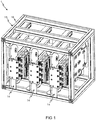
- FIG 1 1 is a perspective view of a converter arrangement 1 according to the invention, in which all three converter modules 14 are electrically conductively connected to a receiving device 15.
- the power converter module 14 arranged on the left is not electrically conductively connected to the receiving device 15 .
- a side view of a direct voltage plug-in connection device 4 of the power converter arrangement 1 is shown in detail, with some of the components of the direct voltage plug-in connection device 4 not being shown.
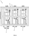
- FIG 4 1 is a side view of the converter arrangement 1, in which the converter module 14 arranged on the left is not electrically conductively connected to the receiving device 15.
- a side view of the DC voltage plug connection device 4 is shown in detail.
- a perspective detailed view of a part of the DC voltage plug-in connection device 4 is shown.
- FIG 7 A perspective view of the power converter module 14 is shown.
- the power converter arrangement 1 has a power converter module 14 having an electrically conductive module negative potential element 2a and an electrically conductive module positive potential element 2b. Between the module negative potential element 2a and the module positive potential element 2b, an electrically non-conductive insulation layer 2c, which can be designed as a plastic film, for example, is preferably arranged.
- the module negative potential element 2a and the module positive potential element 2b are preferably designed as a flat conductor, in particular as sheet metal elements.
- the module negative potential element 2a and the module positive potential element 2b together with the insulating layer 2c form a module DC voltage busbar.
- the power converter module 14 preferably has a power semiconductor module 14a, which has power semiconductor switches that are electrically connected to one another, and a capacitor device 14b, which is electrically conductively connected to the DC voltage connections of the power semiconductor module 14a and has at least one capacitor 14b', with the capacitor device 14b forming an intermediate circuit capacitor.
- the module negative potential element 2a and the module positive potential element 2b are electrically conductively connected to the capacitor device 14b.
- the power semiconductor switches are preferably electrically interconnected to form at least one half-bridge circuit.
- the power converter module 14 also has a module alternating potential element 2d.
- the module negative potential element 2a, the module positive potential element 2b and the module alternating potential element 2d are electrically conductively connected to the power semiconductor switches.
- a DC voltage is present between the module negative potential element 2a and the module positive potential element 2b when the converter arrangement 1 is in operation.
- the power converter arrangement 1 also has an electrically conductive receiving negative potential element 3a and an electrically conductive receiving positive potential element 3b having receiving device 15 for receiving the power converter module 14 .
- the receiving device 15 preferably has, as exemplified in FIGS Figures 1 to 3 shown, a frame member 16 on.
- the frame element 16 can be mounted in a switch cabinet, for example.
- An electrically non-conductive insulation layer 3c which can be embodied, for example, as a plastic film, is preferably arranged between the negative-potential recording element 3a and the positive-potential recording element 3b.
- the recording negative potential element 3a and the recording positive potential element 3b are preferably designed as flat conductors, in particular as sheet metal elements.
- the recording negative potential element 3a and the recording positive potential element 3b together with the insulation layer 2c form a recording DC voltage busbar.
- the module negative potential element 2a and the negative potential element 3a have a negative electrical potential and the module positive potential element 2b and the receptacle positive potential element 3b have a positive electric potential.
- a DC voltage is present between the negative-potential element 3a and the positive-potential element 3b.
- the module negative potential element 2a is electrically conductively connected to the receiving negative potential element 3a and the module positive potential element 2b is electrically conductively connected to the receiving positive potential element 3b via a direct voltage plug-in connection device 4 .
- the power converter module 14 is thus electrically conductively connected to the receiving device 15 via the DC voltage plug-in connection device 4 .
- the power converter module 14 can be quickly and reliably electrically connected to the receiving device 15 and then separated again.
- the power converter arrangement 1 has three power converter modules 14 which are electrically conductively connected to the receiving device 15 via a respective DC voltage plug-in connection device 4 .
- the power converter arrangement 1 according to the invention can also have only a single power converter module 14, which is electrically conductively connected to the receiving device 15 via a DC voltage plug-in connection device 4, or have considerably more power converter modules 14, which are electrically conductively connected to the receiving device 15 via a respective DC voltage plug-in connection device 4.
- the DC voltage plug-in connection device 4 preferably has, as exemplified in 3 and 5 shown in detail, an electrically conductive first connector element 6a, an electrically conductive second connector element 6b arranged electrically insulated from the first connector element 6a, an electrically conductive third connector element 6c and an electrically conductive fourth connector element 6d arranged electrically insulated from the third connector element 6c.
- the first plug-in connection element 6a is in electrically conductive contact with the module negative potential element 2a
- the second plug-in connection element 6b is in electrically conductive contact with the module positive potential element 2b
- the third plug-in connection element 6c is in electrical contact with the receiving negative potential element 3a
- the fourth plug-in connection element 6d is in electrical contact with the receiving positive potential element 3b.
- the respective contact can, for example, by means of a material connection, in particular by means of a soldered or welded connection.
- the respective contacting is preferably implemented in that the first plug-in connection element 6a is formed in one piece with the module negative potential element 2a and the second plug-in connection element 6b with the module positive potential element 2b, and/or in that the third plug-in connection element 6c is formed with the receiving negative potential element 3a and the fourth plug-in connection element 6d with the receiving positive potential element 3b is formed in one piece.
- the first connector element 6a is integral with the module negative potential element 2a and the second connector element 6b is integral with the module positive potential element 2b
- the third connector element 6c is integral with the female negative potential element 3a
- the fourth male connector element 6d is integral with the female positive potential element 3b.
- an electrically non-conductive insulation layer 11 which can be designed as a plastic film, for example, is preferably arranged in one section.
- the insulating layer 11 is preferably formed in one piece with the insulating layer 2c.
- an electrically non-conductive insulation layer 12 which can be in the form of a plastic film, for example.
- the insulation layer 12 is preferably formed in one piece with the insulation layer 3c.
- the first plug-in connection element 6a has a first plug-in connection section 6a' and the second plug-in connection element 6b has a second plug-in connection section 6b' which is arranged at a distance from the first plug-in connection section 6a', with a plug-in connection space 7 being formed between the first and second plug-in connection sections 6a' and 6b'.
- the third plug-in connection element 6c has a third plug-in connection section 6c' and the fourth plug-in connection element 6d has a fourth plug-in connection section 6d', the third and fourth plug-in connection sections 6c' and 6d' being arranged in the plug-in connection space 7.
- the DC voltage plug-in connection device 4 also has an electrically conductive first spring contact device 8 which has an electrically conductive contact with the first plug-in connection section 6a' and has at least one first spring element 8a which presses against the third plug-in connection section 6c'. presses and thereby an electrically conductive pressure contact with the third connector portion 6c 'forms.
- the first spring contact device 8 also preferably has at least one electrically conductive first spring holding element 8b, which holds the at least one first spring element 8a and is electrically conductively contacted with the at least one first spring element 8a.
- the at least one first spring retaining element 8b is in electrically conductive contact with the first plug-in connection section 6a′, in particular in an electrically conductive pressure contact.
- the DC voltage plug-in connection device 4 also has an electrically conductive second spring contact device 9 which has an electrically conductive contact with the second plug-in connection section 6b' and has at least one second spring element 9a which presses against the fourth plug-in connection section 6d' and thereby makes an electrically conductive pressure contact with the fourth plug-in connection section 6d' forms.
- the second spring contact device 9 also preferably has at least one electrically conductive second spring holding element 9b, which holds the at least one second spring element 9a and is electrically conductively contacted with the at least one second spring element 9a.
- the at least one second spring retaining element 9b makes electrically conductive contact with the second plug-in connection section 6b′, in particular makes electrically conductive pressure contact.
- the first plug-in connection element 6a together with the second plug-in connection element 6b forms a socket of the DC voltage plug-in connection device 4 and the third plug-in connection element 6c together with the fourth plug-in connection element 6d forms a plug of the DC voltage plug-in connection device 4.
- the first plug-in connection element 6a together with the second plug-in connection element 6b can form a plug of the DC voltage plug-in connection device 4 and the third plug-in connection element 6c together with the fourth plug-in connection element 6d can form a socket of the DC voltage plug-in connection device 4.
- the first plug-in connection element 6a is connected to the receiving negative potential element 3a, the second plug-in connection element 6b to the receiving positive potential element 3b, the third plug-in connection element 6c with the module negative potential element 2a and the fourth plug-in connection element 6d with the module positive potential element 2b electrically conductively contacted.
- the respective contact can be realized, for example, by means of a material connection, in particular by means of a soldered or welded connection.
- the first plug-in connection element 6a is preferably formed in one piece with the receiving negative potential element 3a and the second plug-in connection element 6b with the receiving positive potential element 3b, and/or the third plug-in connection element 6c is preferably formed in one piece with the module negative potential element 2a and the fourth plug-in connection element 6d is formed in one piece with the module positive potential element 2b.
- this design of the DC voltage plug-in connection device 4 corresponds to the DC voltage plug-in connection device 4 described above, in which the first plug-in connection element 6a together with the second plug-in connection element 6b forms the socket of the DC voltage plug-in connection device 4 and the third plug-in connection element 6c together with the fourth plug-in connection element 6d forms the plug of the DC voltage plug-in connection device 4.
- the first plug-in connection element 6a together with the second plug-in connection element 6b and the third plug-in connection element 6c together with the fourth plug-in connection element 6d are moved towards one another in such a way that the third plug-in connection element 6c together with the fourth plug-in connection element 6d in is inserted into the plug-in connection space 7, so that the at least one first spring element 8a presses against the third plug-in connection section 6c' and thereby forms an electrically conductive pressure contact with the third plug-in connection section 6c' and the at least one second spring element 9a presses against the fourth plug-in connection section 6d' and thereby forms an electrically conductive pressure contact with the fourth connector section 6d'.
- the first plug-in connection element 6a together with the second plug-in connection element 6b and the third plug-in connection element 6c moved away from each other with the fourth connector element 6d in such a way that the third connector element 6c is guided out of the connector space 7 together with the fourth connector element 6d.
- the first, second, third and fourth plug connection elements 6a, 6b, 6c and 6d are preferably designed as flat conductors, in particular as sheet metal elements.
- the first, second, third and fourth plug connection elements 6a, 6b, 6c and 6d are preferably formed at least essentially from copper or from a copper alloy.
- the first spring contact device 8 preferably has a plurality of first spring elements 8a arranged in a row and the second spring contact device 9 has a plurality of second spring elements 9a arranged in a row.
- the DC voltage plug-in connection device 4 preferably has a first clamping device 10a, which presses the first spring contact device 8, more precisely here the at least one first spring holding element 8b, against the first plug-in connection section 6a', so that an electrically conductive pressure contact of the first spring contact device 8 makes contact with the first plug-in connection section 6a', and a second clamping device 10b, which presses the second spring contact device 9, more precisely here the at least one second spring holding element 9b, against the second plug-in connection section 6b', so that an electrically conductive pressure contact of the second spring contact device 9 makes contact with the second plug-in connection section 6b'.
- the DC voltage plug connection device 4 also has, as exemplified in 5 , 6 and FIG 7 shown, in the plug-in connection space 7 there is preferably a first spacer element 13a arranged on the first plug-in connection section 6a' next to the first spring contact device 8 and a second spacer element 13b arranged on the second plug-in connection section 6b' next to the second spring contact device 9.
- the first spacer element 13a has a thickness running in the direction of the third plug-in connection section 6c' such that if the third plug-in connection section 6c' has mechanical contact with the first spacer element 13a, the at least one second spring element 9a still has an electrically conductive pressure contact with the fourth connector portion 6d'.
- the second spacer 13b has a towards the fourth Plug connection section 6d 'to run such thickness that if the fourth plug connection section 6d' has a mechanical contact with the second spacer element 13b, the at least one first spring element 8a still has an electrically conductive pressure contact with the third plug connection section 6c'.
- the DC voltage plug connection device 4 also has, as exemplified in 6 and FIG 7 shown, in the plug-in connection space 7 there is preferably a third spacer element 13c arranged on the first plug-in connection section 6a' next to the first spring contact device 8 and a fourth spacer element 13d arranged on the second plug-in connection section 6b' next to the second spring contact device 9.
- the first spring contact device 8 is arranged between the first and third spacer elements 13a and 13c and the second spring contact device 9 is arranged between the second and fourth spacer elements 13b and 13d.
- the third spacer element 13c has a thickness running in the direction of the third plug-in connection section 6c' such that if the third plug-in connection section 6c' has mechanical contact with the third spacer element 13c, the at least one second spring element 9a still has an electrically conductive pressure contact with the fourth connector portion 6d'.
- the fourth spacer element 13d has such a thickness running in the direction of the fourth plug-in connection section 6d' that if the fourth plug-in connection section 6d' has mechanical contact with the fourth spacer element 13d, the at least one first spring element 8a still has an electrically conductive pressure contact with the third connector portion 6c'.
- the respective spacer elements 13a, 13b, 13c and 13d ensure that, if the third and fourth connector section 6c 'and 6d' are not located in the center of the connector space 7, but based on 5 left or right from the center of the plug-in connection space 7 offset in the plug-in connection space 7, the respective possible offset remains limited in such a way that the at least one first spring element 8a still reliably presses against the third plug-in connection section 6c' and the at least one second spring element 9a still reliably presses against the fourth connector portion 6d'. It is thus ensured that despite manufacturing tolerances of the power converter module 14 and the receiving device 15, the power converter module 14 is reliably electrically conductively connected to the receiving device 15 via the DC voltage plug-in connection device 4 .
- the first spacer element 13a and, if present, the third spacer element 13c preferably tapers, as exemplified in FIG 6 shown, at its end region 13a' or 13c' facing the third and fourth connector section 6c' and 6d' into the connector space 7, when the third and fourth connector section 6c' is inserted.
- the first spacer element 13a and, if present, the third spacer element 13c tapers in the direction of the respective end 13a" or 13c" of the respective end region 13a' or 13c'.
- the second spacer element 13b and, if present, the fourth spacer element 13d preferably tapers, as exemplified in FIG 6 shown, at its end region 13b' or 13d' facing the fourth connector section 6d' when the third and fourth connector sections 6c' and 6d' are inserted into the connector space 7.
- the second spacer element 13b and, if present, the fourth spacer element 13d tapers in the direction of the respective end 13b" or 13d" of the respective end region 13b' or 13d'.
Landscapes
- Engineering & Computer Science (AREA)
- Microelectronics & Electronic Packaging (AREA)
- Dc-Dc Converters (AREA)
Abstract

Description
- Die Erfindung betrifft eine Stromrichteranordnung mit einem ein elektrisch leitendes Modulnegativpotentialelement und ein elektrisch leitendes Modulpositivpotentialelement aufweisenden Stromrichtermodul und mit einer ein elektrisch leitendes Aufnahmenegativpotentialelement und ein elektrisch leitendes Aufnahmepositivpotentialelement aufweisenden Aufnahmeeinrichtung zur Aufnahme des Stromrichtermoduls.
- Aus der
DE 10 2009 051 518 B3 ist eine Stromrichteranordnung mit einem ein elektrisch leitendes Modulnegativpotentialelement und ein elektrisch leitendes Modulpositivpotentialelement aufweisenden Stromrichtermodul und mit einer ein elektrisch leitendes Aufnahmenegativpotentialelement und ein elektrisch leitendes Aufnahmepositivpotentialelement aufweisenden Aufnahmeeinrichtung zur Aufnahme des Stromrichtermoduls, bei der das Modulnegativpotentialelement mit dem Aufnahmenegativpotentialelement und das Modulpositivpotentialelement mit dem Aufnahmepositivpotentialelement mittels einer Schraubverbindung elektrisch leitend verbunden sind. Die Schraubverbindung weist den Nachteil auf, dass das elektrische Verbinden des Stromrichtermoduls mit der Aufnahmeeinrichtung und, z.B. im Falle eines notwenigen Austauschs des Stromrichtermoduls, das elektrische Trennen des Stromrichtermoduls von der Aufnahmeeinrichtung zeitaufwendig ist. - Es ist Aufgabe der Erfindung eine Stromrichteranordnung mit einem Stromrichtermodul und mit einer Aufnahmeeinrichtung zu schaffen, bei der das Stromrichtermodul mit der Aufnahmeeinrichtung schnell und zuverlässig elektrisch leitend verbunden und wieder elektrisch getrennt werden kann.
- Diese Aufgabe wird gelöst durch eine Stromrichteranordnung mit einem ein elektrisch leitendes Modulnegativpotentialelement und ein elektrisch leitendes Modulpositivpotentialelement aufweisenden Stromrichtermodul, mit einer ein elektrisch leitendes Aufnahmenegativpotentialelement und ein elektrisch leitendes Aufnahmepositivpotentialelement aufweisenden Aufnahmeeinrichtung zur Aufnahme des Stromrichtermoduls, wobei das Modulnegativpotentialelement mit dem Aufnahmenegativpotentialelement und das Modulpositivpotentialelement mit dem Aufnahmepositivpotentialelement über eine Gleichspannungsteckverbindungseinrichtung elektrisch leitend verbunden sind.
- Es erweist sich als vorteilhaft, wenn die Gleichspannungsteckverbindungseinrichtung ein elektrisch leitendes erstes Steckverbindungselement, ein vom ersten Steckverbindungselement elektrisch isoliert angeordnetes elektrisch leitendes zweites Steckverbindungselement, ein elektrisch leitendes drittes Steckverbindungselement und ein vom dritten Steckverbindungselement elektrisch isoliertes angeordnetes elektrisch leitendes viertes Steckverbindungselement aufweist, wobei das erste Steckverbindungselement mit dem Modulnegativpotentialelement, das zweite Steckverbindungselement mit dem Modulpositivpotentialelement, das dritte Steckverbindungselement mit dem Aufnahmenegativpotentialelement und das vierte Steckverbindungselement mit dem Aufnahmepositivpotentialelement elektrisch leitend kontaktiert ist, wobei das erste Steckverbindungselement einen ersten Steckverbindungsabschnitt und das zweite Steckverbindungselement einen vom ersten Steckverbindungsabschnitt beabstandet angeordneten zweiten Steckverbindungsabschnitt aufweist, wobei zwischen dem ersten und zweiten Steckverbindungsabschnitt ein Steckverbindungsraum ausgebildet ist, wobei das dritte Steckverbindungselement einen dritten Steckverbindungsabschnitt und das vierte Steckverbindungselement einen vierten Steckverbindungsabschnitt aufweist, wobei der dritte und vierte Steckverbindungsabschnitt im Steckverbindungsraum angeordnet sind, wobei die Gleichspannungsteckverbindungseinrichtung eine mit dem ersten Steckverbindungsabschnitt einen elektrisch leitenden Kontakt aufweisende elektrisch leitende erste Federkontakteinrichtung aufweist, die mindestens ein erstes Federelement aufweist, das gegen den dritten Steckverbindungsabschnitt drückt und hierdurch einen elektrisch leitenden Druckkontakt mit dem dritten Steckverbindungsabschnitt ausbildet, wobei die Gleichspannungsteckverbindungseinrichtung eine mit dem zweiten Steckverbindungsabschnitt einen elektrisch leitenden Kontakt aufweisende elektrisch leitende zweite Federkontakteinrichtung aufweist, die mindestens ein zweites Federelement aufweist, das gegen den vierten Steckverbindungsabschnitt drückt und hierdurch einen elektrisch leitenden Druckkontakt mit dem vierten Steckverbindungsabschnitt ausbildet. Bei dieser Ausbildung der Gleichspannungsteckverbindungseinrichtung bildet das erste Steckverbindungselement zusammen mit dem zweiten Steckverbindungselement eine Buchse der Gleichspannungsteckverbindungseinrichtung aus und das dritte Steckverbindungselement bildet zusammen mit dem vierten Steckverbindungselement einen Stecker der Gleichspannungsteckverbindungseinrichtung aus.
- In diesem Zusammenhang erweist es sich als vorteilhaft, wenn das erste Steckverbindungselement mit dem Modulnegativpotentialelement und das zweite Steckverbindungselement mit dem Modulpositivpotentialelement einstückig ausgebildet ist, und/oder dass das dritte Steckverbindungselement mit dem Aufnahmenegativpotentialelement und das vierte Steckverbindungselement mit dem Aufnahmepositivpotentialelement einstückig ausgebildet ist. Hierdurch ist die Gleichspannungsteckverbindungseinrichtung besonders zuverlässig ausgebildet.
- Weiterhin erweist es sich als vorteilhaft, wenn die Gleichspannungsteckverbindungseinrichtung ein elektrisch leitendes erstes Steckverbindungselement, ein vom ersten Steckverbindungselement elektrisch isoliert angeordnetes elektrisch leitendes zweites Steckverbindungselement, ein elektrisch leitendes drittes Steckverbindungselement und ein vom dritten Steckverbindungselement elektrisch isoliertes angeordnetes elektrisch leitendes viertes Steckverbindungselement aufweist, wobei das erste Steckverbindungselement mit dem Aufnahmenegativpotentialelement, das zweite Steckverbindungselement mit dem Aufnahmepositivpotentialelement, das dritte Steckverbindungselement mit dem Modulnegativpotentialelement und das vierte Steckverbindungselement mit dem Modulpositivpotentialelement elektrisch leitend kontaktiert ist, wobei das erste Steckverbindungselement einen ersten Steckverbindungsabschnitt und das zweite Steckverbindungselement einen vom ersten Steckverbindungsabschnitt 6a' beabstandet angeordneten zweiten Steckverbindungsabschnitt aufweist, wobei zwischen dem ersten und zweiten Steckverbindungsabschnitt ein Steckverbindungsraum ausgebildet ist, wobei das dritte Steckverbindungselement einen dritten Steckverbindungsabschnitt und das vierte Steckverbindungselement einen vierten Steckverbindungsabschnitt aufweist, wobei der dritte und vierte Steckverbindungsabschnitt im Steckverbindungsraum angeordnet sind, wobei die Gleichspannungsteckverbindungseinrichtung eine mit dem ersten Steckverbindungsabschnitt einen elektrisch leitenden Kontakt aufweisende elektrisch leitende erste Federkontakteinrichtung aufweist, die mindestens ein erstes Federelement aufweist, das gegen den dritten Steckverbindungsabschnitt drückt und hierdurch einen elektrisch leitenden Druckkontakt mit dem dritten Steckverbindungsabschnitt ausbildet, wobei die Gleichspannungsteckverbindungseinrichtung eine mit dem zweiten Steckverbindungsabschnitt einen elektrisch leitenden Kontakt aufweisende elektrisch leitende zweite Federkontakteinrichtung aufweist, die mindestens ein zweites Federelement aufweist, das gegen den vierten Steckverbindungsabschnitt drückt und hierdurch einen elektrisch leitenden Druckkontakt mit dem vierten Steckverbindungsabschnitt ausbildet. In diesem Fall bildet das erste Steckverbindungselement zusammen mit dem zweiten Steckverbindungselement einen Stecker der Gleichspannungsteckverbindungseinrichtung aus und das dritte Steckverbindungselement bildet zusammen mit dem vierten Steckverbindungselement eine Buchse der Gleichspannungsteckverbindungseinrichtung aus.
- In diesem Zusammenhang erweist es sich als vorteilhaft, wenn das erste Steckverbindungselement mit dem Aufnahmenegativpotentialelement und das zweite Steckverbindungselement mit dem Aufnahmepositivpotentialelement einstückig ausgebildet ist, und/oder dass das dritte Steckverbindungselement mit dem Modulnegativpotentialelement und das vierte Steckverbindungselement mit dem Modulpositivpotentialelement einstückig ausgebildet ist. Hierdurch ist die Gleichspannungsteckverbindungseinrichtung besonders zuverlässig ausgebildet.
- Weiterhin erweist es sich als vorteilhaft, wenn das erste, zweite, dritte und vierte Steckverbindungselement als Flachleiter ausgebildet sind. Hierdurch ist die Gleichspannungsteckverbindungseinrichtung besonders niederinduktiv ausgebildet.
- Ferner erweist es sich als vorteilhaft, wenn die Gleichspannungsteckverbindungseinrichtung eine erste Klemmeinrichtung aufweist, die die erste Federkontakteinrichtung gegen den ersten Steckverbindungsabschnitt drückt, so dass sich ein elektrisch leitender Druckkontakt der ersten Federkontakteinrichtung mit dem ersten Steckverbindungsabschnitt ausbildet und dass die Gleichspannungsteckverbindungseinrichtung eine zweite Klemmeinrichtung aufweist, die die zweite Federkontakteinrichtung gegen den zweiten Steckverbindungsabschnitt drückt, so dass sich ein elektrisch leitender Druckkontakt der zweiten Federkontakteinrichtung mit dem zweiten Steckverbindungsabschnitt ausbildet. Hierdurch wird das Stromrichtermodul mit der Aufnahmeeinrichtung besonders zuverlässig elektrisch leitend verbunden.
- Ferner erweist es sich als vorteilhaft, wenn die Gleichspannungsteckverbindungseinrichtung im Steckverbindungsraum ein auf dem ersten Steckverbindungsabschnitt neben der ersten Federkontakteinrichtung angeordnetes erstes Abstandselement aufweist und ein auf dem zweiten Steckverbindungsabschnitt neben der zweiten Federkontakteinrichtung angeordnetes zweites Abstandselement aufweist, wobei das erste Abstandselement eine in Richtung auf den dritten Steckverbindungsabschnitt zu verlaufende derartige Dicke aufweist, dass, falls der dritte Steckverbindungsabschnitt einen mechanischen Kontakt mit dem ersten Abstandselement aufweist, das mindestens eine zweite Federelement immer noch einen elektrisch leitenden Druckkontakt mit dem vierten Steckverbindungsabschnitt aufweist, wobei das zweite Abstandselement eine in Richtung auf den vierten Steckverbindungsabschnitt zu verlaufende derartige Dicke aufweist, dass, falls der vierte Steckverbindungsabschnitt einen mechanischen Kontakt mit dem zweiten Abstandselement aufweist, das mindestens eine erste Federelement immer noch einen elektrisch leitenden Druckkontakt mit dem dritten Steckverbindungsabschnitt aufweist. Es ist somit sichergestellt, dass trotz Fertigungstoleranzen des Stromrichtermoduls und der Aufnahmeeinrichtung das Stromrichtermodul mit Aufnahmeeinrichtung über die Gleichspannungsteckverbindungseinrichtung zuverlässig elektrisch leitend verbunden ist.
- In diesem Zusammenhang erweist es sich als vorteilhaft, wenn die Gleichspannungsteckverbindungseinrichtung im Steckverbindungsraum ein auf dem ersten Steckverbindungsabschnitt neben der ersten Federkontakteinrichtung angeordnetes drittes Abstandselement aufweist und ein auf dem zweiten Steckverbindungsabschnitt neben der zweiten Federkontakteinrichtung angeordnetes viertes Abstandselement aufweist, wobei die erste Federkontakteinrichtung zwischen dem ersten und dritten Abstandselement und die zweite Federkontakteinrichtung zwischen dem zweiten und vierten Abstandselement angeordnet ist, wobei das dritte Abstandselement eine in Richtung auf den dritten Steckverbindungsabschnitt zu verlaufende derartige Dicke aufweist, dass, falls der dritte Steckverbindungsabschnitt einen mechanischen Kontakt mit dem dritten Abstandselement aufweist, das mindestens eine zweite Federelement immer noch einen elektrisch leitenden Druckkontakt mit dem vierten Steckverbindungsabschnitt aufweist, wobei das vierte Abstandselement eine in Richtung auf den vierten Steckverbindungsabschnitt zu verlaufende derartige Dicke aufweist, dass, falls der vierte Steckverbindungsabschnitt einen mechanischen Kontakt mit dem vierten Abstandselement aufweist, das mindestens eine erste Federelement immer noch einen elektrisch leitenden Druckkontakt mit dem dritten Steckverbindungsabschnitt aufweist. Es ist somit sichergestellt, das trotz Fertigungstoleranzen des Stromrichtermoduls und der Aufnahmeeinrichtung das Stromrichtermodul mit Aufnahmeeinrichtung über die Gleichspannungsteckverbindungseinrichtung zuverlässig elektrisch leitend verbunden ist.
- Ferner erweist es sich als vorteilhaft, wenn das erste Abstandselement und, falls vorhanden, das dritte Abstandselement sich an seinem bei einem Einführen des dritten und vierten Steckverbindungsabschnitts in den Steckverbindungsraum, dem dritten Steckverbindungsabschnitt zugewandten Endbereich verjüngt.
- Ferner erweist es sich als vorteilhaft, wenn das zweite Abstandselement und, falls vorhanden, das vierte Abstandselement sich an seinem bei einem Einführen des dritten und vierten Steckverbindungsabschnitts in den Steckverbindungsraum, dem vierten Steckverbindungsabschnitt zugewandten Endbereich verjüngt.
- Zum elektrisch leitenden Verbinden des Stromrichtermoduls mit der Aufnahmeeinrichtung werden das erste Steckverbindungselement zusammen mit dem zweiten Steckverbindungselement und das dritte Steckverbindungselement zusammen mit dem vierten Steckverbindungselement derart aufeinander zu bewegt, dass das dritte Steckverbindungselement zusammen mit dem vierten Steckverbindungselement in den Steckverbindungsraum eingeführt wird. Durch die sich verjüngenden Endbereiche der Abstandselemente wird das Einführen des dritten Steckverbindungselements zusammen mit dem vierten Steckverbindungselement in den Steckverbindungsraum erleichtert.
- Weiterhin erweist es sich als vorteilhaft, wenn die erste Federkontakteinrichtung mehrere in einer Reihe angeordnete erste Federelemente aufweist und die zweite Federkontakteinrichtung mehrere in einer Reihe angeordnete zweite Federelemente aufweist. Hierdurch ist das Stromrichtermodul mit der Aufnahmeeinrichtung besonders zuverlässig elektrisch leitend verbunden.
- Ferner erweist es sich als vorteilhaft, wenn das Stromrichtermodul ein Leistungshalbleitermodul, das miteinander elektrisch verschaltete Leistungshalbeiterschalter aufweist, und eine mit Gleichspannungsanschlüssen des Leistungshalbleitermoduls elektrisch leitend verbundene, mindestens einen Kondensator aufweisende Kondensatoreinrichtung aufweist, wobei die Kondensatoreinrichtung einen Zwischenkreiskondensator ausbildet.
- Ein Ausführungsbeispiel der Erfindung wird nachfolgend unter Bezugnahme auf die unten stehenden Figuren erläutert. Dabei zeigen:
- FIG 1
- eine perspektivische Ansicht einer erfindungsgemäßen Stromrichteranordnung bei der alle drei Stromrichtermodule mit einer Aufnahmeeinrichtung elektrisch leitend verbunden sind,
- FIG 2
- eine perspektivische Ansicht einer erfindungsgemäßen Stromrichteranordnung bei der das links angeordnete Stromrichtermodul mit der Aufnahmeeinrichtung nicht elektrisch leitend verbunden ist,
- FIG 3
- eine Seitenansicht von wesentlichen Teilen einer Gleichspannungsteckverbindungseinrichtung der erfindungsgemäßen Stromrichteranordnung und der die Gleichspannungsteckverbindungseinrichtung umgebenden Elemente der Stromrichteranordnung.
- FIG 4
- eine Seitenansicht der erfindungsgemäßen Stromrichteranordnung, bei der das links angeordnete Stromrichtermodul mit der Aufnahmeeinrichtung nicht elektrisch leitend verbunden ist,
- FIG 5
- eine Seitenansicht der Gleichspannungsteckverbindungseinrichtung der erfindungsgemäßen Stromrichteranordnung und der die Gleichspannungsteckverbindungseinrichtung umgebenden Elemente,
- FIG 6
- eine perspektivische Detailansicht eines Teils der Gleichspannungsteckverbindungseinrichtung und
- FIG 7
- eine perspektivische Ansicht eines Stromrichtermoduls der erfindungsgemäßen Stromrichteranordnung.
- In
FIG 1 ist eine perspektivische Ansicht einer erfindungsgemäßen Stromrichteranordnung 1, bei der alle drei Stromrichtermodule 14 mit einer Aufnahmeeinrichtung 15 elektrisch leitend verbunden sind, dargestellt. InFIG 2 ist das links angeordnete Stromrichtermodul 14 mit der Aufnahmeeinrichtung 15 nicht elektrisch leitend verbunden. InFIG 3 ist eine Seitenansicht einer Gleichspannungsteckverbindungseinrichtung 4 der Stromrichteranordnung 1 im Detail dargestellt, wobei ein Teil der Bauelemente der Gleichspannungsteckverbindungseinrichtung 4 nicht dargestellt ist. InFIG 4 ist eine Seitenansicht der Stromrichteranordnung 1, bei der das links angeordnete Stromrichtermodul 14 mit der Aufnahmeeinrichtung 15 nicht elektrisch leitend verbunden ist, dargestellt. InFIG 5 ist eine Seitenansicht der Gleichspannungsteckverbindungseinrichtung 4 im Detail dargestellt. InFIG 6 ist eine perspektivische Detailansicht eines Teils der Gleichspannungsteckverbindungseinrichtung 4 dargestellt. InFIG 7 ist eine perspektivische Ansicht des Stromrichtermoduls 14 dargestellt. - Die erfindungsgemäße Stromrichteranordnung 1 weist ein elektrisch leitendes Modulnegativpotentialelement 2a und ein elektrisch leitendes Modulpositivpotentialelement 2b aufweisendes Stromrichtermodul 14 auf. Zwischen dem Modulnegativpotentialelement 2a und dem Modulpositivpotentialelement 2b ist vorzugweise eine elektrisch nicht leitende Isolationsschicht 2c, die z.B. als Kunststofffolie ausgebildet sein kann, angeordnet. Das Modulnegativpotentialelement 2a und das Modulpositivpotentialelement 2b sind vorzugsweise als Flachleiter, insbesondere als Blechelemente, ausgebildet. Das Modulnegativpotentialelement 2a und das Modulpositivpotentialelement 2b bilden zusammen mit der Isolationsschicht 2c eine Modulgleichspannungsverschienung aus. Wie beispielhaft in
FIG 7 dargestellt, weist das Stromrichtermodul 14 vorzugsweise ein Leistungshalbleitermodul 14a, das miteinander elektrisch verschaltete Leistungshalbeiterschalter aufweist und eine mit Gleichspannungsanschlüssen des Leistungshalbleitermoduls 14a elektrisch leitend verbundene, mindestens einen Kondensator 14b' aufweisende Kondensatoreinrichtung 14b auf, wobei die Kondensatoreinrichtung 14b einen Zwischenkreiskondensator ausbildet. Das Modulnegativpotentialelement 2a, das Modulpositivpotentialelement 2b sind mit der Kondensatoreinrichtung 14b elektrisch leitend verbunden. Die Leistungshalbeiterschalter sind vorzugsweise elektrisch zu mindestens einer Halbbrückenschaltung verschalten. Das Stromrichtermodul 14 weist weiterhin ein Modulwechselpotentialelement 2d auf. Das Modulnegativpotentialelement 2a, das Modulpositivpotentialelement 2b und das Modulwechselpotentialelement 2d sind mit den Leistungshalbeiterschaltern elektrisch leitend verbunden. Zwischen dem Modulnegativpotentialelement 2a und dem Modulpositivpotentialelement 2b liegt im Betrieb der Stromrichteranordnung 1 eine Gleichspannung an. - Die Stromrichteranordnung 1 weist weiterhin ein elektrisch leitendes Aufnahmenegativpotentialelement 3a und ein elektrisch leitendes Aufnahmepositivpotentialelement 3b aufweisende Aufnahmeeinrichtung 15 zur Aufnahme des Stromrichtermoduls 14 auf. Die Aufnahmeeinrichtung 15 weist vorzugsweise, wie beispielhaft in den
Figuren 1 bis 3 dargestellt, ein Rahmenelement 16 auf. Das Rahmenelement 16 kann z.B. in einem Schaltschrank montiert sein. Zwischen dem Aufnahmenegativpotentialelement 3a und dem Aufnahmepositivpotentialelement 3b ist vorzugweise eine elektrisch nicht leitende Isolationsschicht 3c, die z.B. als Kunststofffolie ausgebildet sein kann, angeordnet. Das Aufnahmenegativpotentialelement 3a und das Aufnahmepositivpotentialelement 3b sind vorzugsweise als Flachleiter, insbesondere als Blechelemente, ausgebildet. Das Aufnahmenegativpotentialelement 3a und das Aufnahmepositivpotentialelement 3b bilden zusammen mit der Isolationsschicht 2c eine Aufnahmegleichspannungsverschienung aus. - Im Betrieb der Stromrichteranordnung 1 weisen das Modulnegativpotentialelement 2a und das Aufnahmenegativpotentialelement 3a ein negatives elektrisches Potential auf und das Modulpositivpotentialelement 2b und das Aufnahmepositivpotentialelement 3b ein positives elektrisches Potential auf. Zwischen dem Aufnahmenegativpotentialelement 3a und dem Aufnahmepositivpotentialelement 3b liegt im Betrieb der Stromrichteranordnung 1 eine Gleichspannung an.
- Das Modulnegativpotentialelement 2a ist mit dem Aufnahmenegativpotentialelement 3a und das Modulpositivpotentialelement 2b ist mit dem Aufnahmepositivpotentialelement 3b über eine Gleichspannungsteckverbindungseinrichtung 4 elektrisch leitend verbunden. Bei der Erfindung ist somit das Stromrichtermodul 14 mit der Aufnahmeeinrichtung 15 über die Gleichspannungsteckverbindungseinrichtung 4 elektrisch leitend verbunden. Hierdurch kann das Stromrichtermodul 14 mit der Aufnahmeeinrichtung 15 schnell und zuverlässig elektrisch leitend verbunden und wieder getrennt werden.
- Im Rahmen des Ausführungsbeispiels weist die Stromrichteranordnung 1 drei Stromrichtermodule 14 auf, die mit der Aufnahmeeinrichtung 15 über eine jeweilige Gleichspannungsteckverbindungseinrichtung 4 elektrisch leitend verbunden sind. Selbstverständlich kann die erfindungsgemäße Stromrichteranordnung 1 auch nur ein einzelnes Stromrichtermodul 14 aufweisen, das mit der Aufnahmeeinrichtung 15 über eine Gleichspannungsteckverbindungseinrichtung 4 elektrisch leitend verbunden ist oder noch erheblich mehr Stromrichtermodule 14 aufweisen, die mit der Aufnahmeeinrichtung 15 über eine jeweilige Gleichspannungsteckverbindungseinrichtung 4 elektrisch leitend verbunden sind.
- Die Gleichspannungsteckverbindungseinrichtung 4 weist vorzugsweise, wie beispielhaft in
FIG 3 undFIG 5 im Detail dargestellt, ein elektrisch leitendes erstes Steckverbindungselement 6a, ein vom ersten Steckverbindungselement 6a elektrisch isoliert angeordnetes elektrisch leitendes zweites Steckverbindungselement 6b, ein elektrisch leitendes drittes Steckverbindungselement 6c und ein vom dritten Steckverbindungselement 6c elektrisch isoliertes angeordnetes elektrisch leitendes viertes Steckverbindungselement 6d auf. Das erste Steckverbindungselement 6a ist mit dem Modulnegativpotentialelement 2a, das zweite Steckverbindungselement 6b ist mit dem Modulpositivpotentialelement 2b, das dritte Steckverbindungselement 6c ist mit dem Aufnahmenegativpotentialelement 3a und das vierte Steckverbindungselement 6d ist mit dem Aufnahmepositivpotentialelement 3b elektrisch leitend kontaktiert. Die jeweilige Kontaktierung kann z.B. mittels einer stoffschlüssigen Verbindung, insbesondere mittels einer Löt- oder Schweißverbindung, realisiert sein. Die jeweilige Kontaktierung ist vorzugsweise realisiert, indem das erste Steckverbindungselement 6a mit dem Modulnegativpotentialelement 2a und das zweite Steckverbindungselement 6b mit dem Modulpositivpotentialelement 2b einstückig ausgebildet ist, und/oder indem das dritte Steckverbindungselement 6c mit dem Aufnahmenegativpotentialelement 3a und das vierte Steckverbindungselement 6d mit dem Aufnahmepositivpotentialelement 3b einstückig ausgebildet ist. Beim Ausführungsbeispiel ist das erste Steckverbindungselement 6a mit dem Modulnegativpotentialelement 2a und das zweite Steckverbindungselement 6b ist mit dem Modulpositivpotentialelement 2b einstückig ausgebildet, und das dritte Steckverbindungselement 6c ist mit dem Aufnahmenegativpotentialelement 3a und das vierte Steckverbindungselement 6d ist mit dem Aufnahmepositivpotentialelement 3b einstückig ausgebildet. Zwischen dem ersten Steckverbindungselement 6a und dem zweiten Steckverbindungselement 6b ist vorzugsweise in einem Abschnitt eine elektrisch nicht leitende Isolationsschicht 11, die z.B. als Kunststofffolie ausgebildet sein kann, angeordnet. Die Isolationsschicht 11 ist vorzugsweise mit der Isolationsschicht 2c einstückig ausgebildet. Zwischen dem dritten Steckverbindungselement 6c und dem vierten Steckverbindungselement 6d ist vorzugsweise eine elektrisch nicht leitende Isolationsschicht 12, die z.B. als Kunststofffolie ausgebildet sein kann, angeordnet. Die Isolationsschicht 12 ist vorzugsweise mit der Isolationsschicht 3c einstückig ausgebildet. - Das erste Steckverbindungselement 6a weist einen ersten Steckverbindungsabschnitt 6a' und das zweite Steckverbindungselement 6b einen vom ersten Steckverbindungsabschnitt 6a' beabstandet angeordneten zweiten Steckverbindungsabschnitt 6b' auf, wobei zwischen dem ersten und zweiten Steckverbindungsabschnitt 6a' und 6b' ein Steckverbindungsraum 7 ausgebildet ist. Das dritte Steckverbindungselement 6c weist einen dritten Steckverbindungsabschnitt 6c' und das vierte Steckverbindungselement 6d einen vierten Steckverbindungsabschnitt 6d' auf, wobei der dritte und vierte Steckverbindungsabschnitt 6c' und 6d' im Steckverbindungsraum 7 angeordnet sind.
- Die Gleichspannungsteckverbindungseinrichtung 4 weist weiterhin eine mit dem ersten Steckverbindungsabschnitt 6a' einen elektrisch leitenden Kontakt aufweisende elektrisch leitende erste Federkontakteinrichtung 8 auf, die mindestens ein erstes Federelement 8a aufweist, das gegen den dritten Steckverbindungsabschnitt 6c' drückt und hierdurch einen elektrisch leitenden Druckkontakt mit dem dritten Steckverbindungsabschnitt 6c' ausbildet. Die erste Federkontakteinrichtung 8 weist weiterhin vorzugsweise mindestens ein elektrisch leitendes erstes Federhalteelement 8b auf, das das mindestens eine erste Federelement 8a hält und mit dem mindestens einen ersten Federelement 8a elektrisch leitend kontaktiert ist. Das mindestens eine erste Federhalteelement 8b ist mit dem ersten Steckverbindungsabschnitt 6a' elektrisch leitend kontaktiert, insbesondere elektrisch leitend druckkontaktiert. Die Gleichspannungsteckverbindungseinrichtung 4 weist weiterhin eine mit dem zweiten Steckverbindungsabschnitt 6b' einen elektrisch leitenden Kontakt aufweisende elektrisch leitende zweite Federkontakteinrichtung 9 auf, die mindestens ein zweites Federelement 9a aufweist, das gegen den vierten Steckverbindungsabschnitt 6d' drückt und hierdurch einen elektrisch leitenden Druckkontakt mit dem vierten Steckverbindungsabschnitt 6d' ausbildet. Die zweite Federkontakteinrichtung 9 weist weiterhin vorzugsweise mindestens ein elektrisch leitendes zweites Federhalteelement 9b auf, das das mindestens eine zweite Federelement 9a hält und mit dem mindestens einen zweiten Federelement 9a elektrisch leitend kontaktiert ist. Das mindestens eine zweite Federhalteelement 9b ist mit dem zweiten Steckverbindungsabschnitt 6b' elektrisch leitend kontaktiert, insbesondere elektrisch leitend druckkontaktiert.
- Bei oben beschriebener Gleichspannungsteckverbindungseinrichtung 4 bildet das erste Steckverbindungselement 6a zusammen mit dem zweiten Steckverbindungselement 6b eine Buchse der Gleichspannungsteckverbindungseinrichtung 4 aus und das dritte Steckverbindungselement 6c bildet zusammen mit dem vierten Steckverbindungselement 6d einen Stecker der Gleichspannungsteckverbindungseinrichtung 4 aus.
- Alternativ kann, wie nachfolgend beschrieben, das erste Steckverbindungselement 6a zusammen mit dem zweiten Steckverbindungselement 6b einen Stecker der Gleichspannungsteckverbindungseinrichtung 4 ausbilden und das dritte Steckverbindungselement 6c zusammen mit dem vierten Steckverbindungselement 6d eine Buchse der Gleichspannungsteckverbindungseinrichtung 4 ausbilden. Bei dieser Ausbildung der Gleichspannungsteckverbindungseinrichtung 4, die in den Figuren nicht dargestellt ist, ist das erste Steckverbindungselement 6a mit dem Aufnahmenegativpotentialelement 3a, das zweite Steckverbindungselement 6b mit dem Aufnahmepositivpotentialelement 3b, das dritte Steckverbindungselement 6c mit dem Modulnegativpotentialelement 2a und das vierte Steckverbindungselement 6d mit dem Modulpositivpotentialelement 2b elektrisch leitend kontaktiert. Die jeweilige Kontaktierung kann z.B. mittels einer stoffschlüssigen Verbindung, insbesondere mittels einer Löt- oder Schweißverbindung, realisiert sein. Das erste Steckverbindungselement 6a ist vorzugsweise mit dem Aufnahmenegativpotentialelement 3a und das zweite Steckverbindungselement 6b mit dem Aufnahmepositivpotentialelement 3b einstückig ausgebildet, und/oder das dritte Steckverbindungselement 6c ist vorzugsweise mit dem Modulnegativpotentialelement 2a und das vierte Steckverbindungselement 6d ist mit dem Modulpositivpotentialelement 2b einstückig ausgebildet. Ansonsten entspricht diese Ausbildung der Gleichspannungsteckverbindungseinrichtung 4 der oben beschriebenen Gleichspannungsteckverbindungseinrichtung 4 bei der das erste Steckverbindungselement 6a zusammen mit dem zweiten Steckverbindungselement 6b die Buchse der Gleichspannungsteckverbindungseinrichtung 4 und das dritte Steckverbindungselement 6c zusammen mit dem vierten Steckverbindungselement 6d den Stecker der Gleichspannungsteckverbindungseinrichtung 4 ausbildet.
- Die nachfolgende Beschreibung bezieht sich jeweils auf beide oben beschriebenen Ausbildungen der Gleichspannungsteckverbindungseinrichtung 4.
- Zum elektrisch leitenden Verbinden des Stromrichtermoduls 14 mit der Aufnahmeeinrichtung 15 werden das erste Steckverbindungselement 6a zusammen mit dem zweiten Steckverbindungselement 6b und das dritte Steckverbindungselement 6c zusammen mit dem vierten Steckverbindungselement 6d derart aufeinander zu bewegt, dass das dritte Steckverbindungselement 6c zusammen mit dem vierten Steckverbindungselement 6d in den Steckverbindungsraum 7 eingeführt wird, so dass das mindestens eine erste Federelement 8a gegen den dritten Steckverbindungsabschnitt 6c' drückt und hierdurch einen elektrisch leitenden Druckkontakt mit dem dritten Steckverbindungsabschnitt 6c' ausbildet und das mindestens eine zweite Federelement 9a gegen den vierten Steckverbindungsabschnitt 6d' drückt und hierdurch einen elektrisch leitenden Druckkontakt mit dem vierten Steckverbindungsabschnitt 6d' ausbildet. Zum elektrischen Trennen des Stromrichtermoduls 14 von der Aufnahmeeinrichtung 15 werden das erste Steckverbindungselement 6a zusammen mit dem zweiten Steckverbindungselement 6b und das dritte Steckverbindungselement 6c zusammen mit dem vierten Steckverbindungselement 6d derart voneinander weg bewegt, dass das dritte Steckverbindungselement 6c zusammen mit dem vierten Steckverbindungselement 6d aus den Steckverbindungsraum 7 herausgeführt wird.
- Das erste, zweite, dritte und vierte Steckverbindungselement 6a, 6b, 6c und 6d sind vorzugsweise als Flachleiter, insbesondere als Blechelemente, ausgebildet. Das erste, zweite, dritte und vierte Steckverbindungselement 6a, 6b, 6c und 6d sind vorzugsweise zumindest im Wesentlichen aus Kupfer oder aus einer Kupferlegierung ausgebildet.
- Die erste Federkontakteinrichtung 8 weist vorzugsweise mehrere in einer Reihe angeordnete erste Federelemente 8a und die zweite Federkontakteinrichtung 9 mehrere in einer Reihe angeordnete zweite Federelemente 9a auf.
- Die Gleichspannungsteckverbindungseinrichtung 4 weist vorzugsweise eine erste Klemmeinrichtung 10a auf, die die erste Federkontakteinrichtung 8, genauer ausgedrückt hier das mindestens eine erste Federhalteelement 8b, gegen den ersten Steckverbindungsabschnitt 6a' drückt, so dass sich ein elektrisch leitender Druckkontakt der ersten Federkontakteinrichtung 8 mit dem ersten Steckverbindungsabschnitt 6a' ausbildet, und eine zweite Klemmeinrichtung 10b auf, die die zweite Federkontakteinrichtung 9, genauer ausgedrückt hier das mindestens eine zweite Federhalteelement 9b, gegen den zweiten Steckverbindungsabschnitt 6b' drückt, so dass sich ein elektrisch leitender Druckkontakt der zweiten Federkontakteinrichtung 9 mit dem zweiten Steckverbindungsabschnitt 6b' ausbildet.
- Die Gleichspannungsteckverbindungseinrichtung 4 weist weiterhin, wie beispielhaft in
FIG 5 ,FIG 6 undFIG 7 dargestellt, im Steckverbindungsraum 7 vorzugsweise ein auf dem ersten Steckverbindungsabschnitt 6a' neben der ersten Federkontakteinrichtung 8 angeordnetes erstes Abstandselement 13a und ein auf dem zweiten Steckverbindungsabschnitt 6b' neben der zweiten Federkontakteinrichtung 9 angeordnetes zweites Abstandselement 13b auf. Das erste Abstandselement 13a weist eine in Richtung auf den dritten Steckverbindungsabschnitt 6c' zu verlaufende derartige Dicke auf, dass, falls der dritte Steckverbindungsabschnitt 6c' einen mechanischen Kontakt mit dem ersten Abstandselement 13a aufweist, das mindestens eine zweite Federelement 9a immer noch einen elektrisch leitenden Druckkontakt mit dem vierten Steckverbindungsabschnitt 6d' aufweist. Das zweite Abstandselement 13b weist eine in Richtung auf den vierten Steckverbindungsabschnitt 6d' zu verlaufende derartige Dicke auf, dass, falls der vierte Steckverbindungsabschnitt 6d' einen mechanischen Kontakt mit dem zweiten Abstandselement 13b aufweist, das mindestens eine erste Federelement 8a immer noch einen elektrisch leitenden Druckkontakt mit dem dritten Steckverbindungsabschnitt 6c' aufweist. - Die Gleichspannungsteckverbindungseinrichtung 4 weist weiterhin, wie beispielhaft in
FIG 6 undFIG 7 dargestellt, im Steckverbindungsraum 7 vorzugsweise ein auf dem ersten Steckverbindungsabschnitt 6a' neben der ersten Federkontakteinrichtung 8 angeordnetes drittes Abstandselement 13c und ein auf dem zweiten Steckverbindungsabschnitt 6b' neben der zweiten Federkontakteinrichtung 9 angeordnetes viertes Abstandselement 13d auf. Die erste Federkontakteinrichtung 8 ist zwischen dem ersten und dritten Abstandselement 13a und 13c und die zweite Federkontakteinrichtung 9 ist zwischen dem zweiten und vierten Abstandselement 13b und 13d angeordnet. Das dritte Abstandselement 13c weist eine in Richtung auf den dritten Steckverbindungsabschnitt 6c' zu verlaufende derartige Dicke auf, dass, falls der dritte Steckverbindungsabschnitt 6c' einen mechanischen Kontakt mit dem dritten Abstandselement 13c aufweist, das mindestens eine zweite Federelement 9a immer noch einen elektrisch leitenden Druckkontakt mit dem vierten Steckverbindungsabschnitt 6d' aufweist. Das vierte Abstandselement 13d weist eine in Richtung auf den vierten Steckverbindungsabschnitt 6d' zu verlaufende derartige Dicke auf, dass, falls der vierte Steckverbindungsabschnitt 6d' einen mechanischen Kontakt mit dem vierten Abstandselement 13d aufweist, das mindestens eine erste Federelement 8a immer noch einen elektrisch leitenden Druckkontakt mit dem dritten Steckverbindungsabschnitt 6c' aufweist. - Die jeweiligen Abstandselemente 13a, 13b, 13c bzw. 13d stellen sicher, dass, falls der dritte und vierte Steckverbindungsabschnitt 6c' und 6d' nicht im Steckverbindungsraum 7 mittig angeordnet sind, sondern bezogen auf
FIG 5 links oder rechts aus der Mitte des Steckverbindungsraums 7 versetzt im Steckverbindungsraum 7 angeordnet sind, der jeweilig mögliche Versatz derartig begrenzt bleibt, dass das mindestens eine erste Federelement 8a immer noch zuverlässig gegen den dritten Steckverbindungsabschnitt 6c' drückt und das mindestens eine zweite Federelement 9a immer noch zuverlässig gegen den vierten Steckverbindungsabschnitt 6d' drückt. Es ist somit sichergestellt, das trotz Fertigungstoleranzen des Stromrichtermoduls 14 und der Aufnahmeeinrichtung 15, das Stromrichtermodul 14 mit Aufnahmeeinrichtung 15 über die Gleichspannungsteckverbindungseinrichtung 4 zuverlässig elektrisch leitend verbunden sind. - Das erste Abstandselement 13a und, falls vorhanden, das dritte Abstandselement 13c verjüngt sich vorzugsweise, wie beispielhaft in
FIG 6 dargestellt, an seinem bei einem Einführen des dritten und vierten Steckverbindungsabschnitts 6c' und 6d' in den Steckverbindungsraum 7, dem dritten Steckverbindungsabschnitt 6c' zugewandten Endbereich 13a' bzw. 13c'. Das erste Abstandselement 13a und, falls vorhanden, das dritte Abstandselement 13c verjüngt sich in Richtung auf das jeweilige Ende 13a" bzw. 13c" des jeweiligen Endbereichs 13a' bzw. 13c' zu. - Das zweite Abstandselement 13b und, falls vorhanden, das vierte Abstandselement 13d verjüngt sich vorzugsweise, wie beispielhaft in
FIG 6 dargestellt, an seinem bei einem Einführen des dritten und vierten Steckverbindungsabschnitts 6c' und 6d' in den Steckverbindungsraum 7, dem vierten Steckverbindungsabschnitt 6d' zugewandten Endbereich 13b' bzw. 13d'. Das zweite Abstandselement 13b und, falls vorhanden, das vierte Abstandselement 13d verjüngt sich in Richtung auf das jeweilige Ende 13b" bzw. 13d" des jeweiligen Endbereichs 13b' bzw. 13d' zu.
Claims (13)
- Stromrichteranordnung mit einem ein elektrisch leitendes Modulnegativpotentialelement (2a) und ein elektrisch leitendes Modulpositivpotentialelement (2b) aufweisenden Stromrichtermodul (14), mit einer ein elektrisch leitendes Aufnahmenegativpotentialelement (3a) und ein elektrisch leitendes Aufnahmepositivpotentialelement (3b) aufweisenden Aufnahmeeinrichtung (15) zur Aufnahme des Stromrichtermoduls (14), wobei das Modulnegativpotentialelement (2a) mit dem Aufnahmenegativpotentialelement (3a) und das Modulpositivpotentialelement (2b) mit dem Aufnahmepositivpotentialelement (3b) über eine Gleichspannungsteckverbindungseinrichtung (4) elektrisch leitend verbunden sind.
- Stromrichteranordnung nach Anspruch 1, dadurch gekennzeichnet, dass die Gleichspannungsteckverbindungseinrichtung (4) ein elektrisch leitendes erstes Steckverbindungselement (6a), ein vom ersten Steckverbindungselement (6a) elektrisch isoliert angeordnetes elektrisch leitendes zweites Steckverbindungselement (6b), ein elektrisch leitendes drittes Steckverbindungselement (6c) und ein vom dritten Steckverbindungselement (6c) elektrisch isoliertes angeordnetes elektrisch leitendes viertes Steckverbindungselement (6d) aufweist, wobei das erste Steckverbindungselement (6a) mit dem Modulnegativpotentialelement (2a), das zweite Steckverbindungselement (6b) mit dem Modulpositivpotentialelement (2b), das dritte Steckverbindungselement (6c) mit dem Aufnahmenegativpotentialelement (3a) und das vierte Steckverbindungselement (6d) mit dem Aufnahmepositivpotentialelement (3b) elektrisch leitend kontaktiert ist, wobei das erste Steckverbindungselement (6a) einen ersten Steckverbindungsabschnitt (6a') und das zweite Steckverbindungselement (6b) einen vom ersten Steckverbindungsabschnitt (6a') beabstandet angeordneten zweiten Steckverbindungsabschnitt (6b') aufweist, wobei zwischen dem ersten und zweiten Steckverbindungsabschnitt (6a',6b') ein Steckverbindungsraum (7) ausgebildet ist, wobei das dritte Steckverbindungselement (6c) einen dritten Steckverbindungsabschnitt (6c') und das vierte Steckverbindungselement (6d) einen vierten Steckverbindungsabschnitt (6d') aufweist, wobei der dritte und vierte Steckverbindungsabschnitt (6c',6d') im Steckverbindungsraum (7) angeordnet sind, wobei die Gleichspannungsteckverbindungseinrichtung (4) eine mit dem ersten Steckverbindungsabschnitt (6a') einen elektrisch leitenden Kontakt aufweisende elektrisch leitende erste Federkontakteinrichtung (8) aufweist, die mindestens ein erstes Federelement (8a) aufweist, das gegen den dritten Steckverbindungsabschnitt (6c') drückt und hierdurch einen elektrisch leitenden Druckkontakt mit dem dritten Steckverbindungsabschnitt (6c') ausbildet, wobei die Gleichspannungsteckverbindungseinrichtung (4) eine mit dem zweiten Steckverbindungsabschnitt (6b') einen elektrisch leitenden Kontakt aufweisende elektrisch leitende zweite Federkontakteinrichtung (9) aufweist, die mindestens ein zweites Federelement (9a) aufweist, das gegen den vierten Steckverbindungsabschnitt (6d') drückt und hierdurch einen elektrisch leitenden Druckkontakt mit dem vierten Steckverbindungsabschnitt (6d') ausbildet.
- Stromrichteranordnung nach Anspruch 2, dadurch gekennzeichnet, dass das erste Steckverbindungselement (6a) mit dem Modulnegativpotentialelement (2a) und das zweite Steckverbindungselement (6b) mit dem Modulpositivpotentialelement (2b) einstückig ausgebildet ist, und/oder dass das dritte Steckverbindungselement (6c) mit dem Aufnahmenegativpotentialelement (3a) und das vierte Steckverbindungselement (6d) mit dem Aufnahmepositivpotentialelement (3b) einstückig ausgebildet ist.
- Stromrichteranordnung nach Anspruch 1, dadurch gekennzeichnet, dass die Gleichspannungsteckverbindungseinrichtung (4) ein elektrisch leitendes erstes Steckverbindungselement (6a), ein vom ersten Steckverbindungselement (6a) elektrisch isoliert angeordnetes elektrisch leitendes zweites Steckverbindungselement (6b), ein elektrisch leitendes drittes Steckverbindungselement (6c) und ein vom dritten Steckverbindungselement (6c) elektrisch isoliertes angeordnetes elektrisch leitendes viertes Steckverbindungselement (6d) aufweist, wobei das erste Steckverbindungselement (6a) mit dem Aufnahmenegativpotentialelement (3a), das zweite Steckverbindungselement (6b) mit dem Aufnahmepositivpotentialelement (3b), das dritte Steckverbindungselement (6c) mit dem Modulnegativpotentialelement (2a) und das vierte Steckverbindungselement (6d) mit dem Modulpositivpotentialelement (2b) elektrisch leitend kontaktiert ist, wobei das erste Steckverbindungselement (6a) einen ersten Steckverbindungsabschnitt (6a') und das zweite Steckverbindungselement (6b) einen vom ersten Steckverbindungsabschnitt (6a') beabstandet angeordneten zweiten Steckverbindungsabschnitt (6b') aufweist, wobei zwischen dem ersten und zweiten Steckverbindungsabschnitt (6a',6b') ein Steckverbindungsraum (7) ausgebildet ist, wobei das dritte Steckverbindungselement (6c) einen dritten Steckverbindungsabschnitt (6c') und das vierte Steckverbindungselement (6d) einen vierten Steckverbindungsabschnitt (6d') aufweist, wobei der dritte und vierte Steckverbindungsabschnitt (6c',6d') im Steckverbindungsraum (7) angeordnet sind, wobei die Gleichspannungsteckverbindungseinrichtung (4) eine mit dem ersten Steckverbindungsabschnitt (6a') einen elektrisch leitenden Kontakt aufweisende elektrisch leitende erste Federkontakteinrichtung (8) aufweist, die mindestens ein erstes Federelement (8a) aufweist, das gegen den dritten Steckverbindungsabschnitt (6c') drückt und hierdurch einen elektrisch leitenden Druckkontakt mit dem dritten Steckverbindungsabschnitt (6c') ausbildet, wobei die Gleichspannungsteckverbindungseinrichtung (4) eine mit dem zweiten Steckverbindungsabschnitt (6b') einen elektrisch leitenden Kontakt aufweisende elektrisch leitende zweite Federkontakteinrichtung (9) aufweist, die mindestens ein zweites Federelement (9a) aufweist, das gegen den vierten Steckverbindungsabschnitt (6d') drückt und hierdurch einen elektrisch leitenden Druckkontakt mit dem vierten Steckverbindungsabschnitt (6d') ausbildet.
- Stromrichteranordnung nach Anspruch 4, dadurch gekennzeichnet, dass das erste Steckverbindungselement (6a) mit dem Aufnahmenegativpotentialelement (3a) und das zweite Steckverbindungselement (6b) mit dem Aufnahmepositivpotentialelement (3b) einstückig ausgebildet ist, und/oder dass das dritte Steckverbindungselement (6c) mit dem Modulnegativpotentialelement (2a) und das vierte Steckverbindungselement (6d) mit dem Modulpositivpotentialelement (2b) einstückig ausgebildet ist.
- Stromrichteranordnung nach einem der Ansprüche 2 bis 5, dadurch gekennzeichnet, dass das erste, zweite, dritte und vierte Steckverbindungselement (6a,6b,6c,6d) als Flachleiter ausgebildet sind.
- Stromrichteranordnung nach einem der Ansprüche 2 bis 6, dadurch gekennzeichnet, dass die Gleichspannungsteckverbindungseinrichtung (4) eine erste Klemmeinrichtung (10a) aufweist, die die erste Federkontakteinrichtung (8) gegen den ersten Steckverbindungsabschnitt (6a') drückt, so dass sich ein elektrisch leitender Druckkontakt der ersten Federkontakteinrichtung (8) mit dem ersten Steckverbindungsabschnitt (6a') ausbildet und dass die Gleichspannungsteckverbindungseinrichtung (4) eine zweite Klemmeinrichtung (10b) aufweist, die die zweite Federkontakteinrichtung (9) gegen den zweiten Steckverbindungsabschnitt (6b') drückt, so dass sich ein elektrisch leitender Druckkontakt der zweiten Federkontakteinrichtung (9) mit dem zweiten Steckverbindungsabschnitt (6b') ausbildet.
- Stromrichteranordnung nach einem der Ansprüche 2 bis 7, dadurch gekennzeichnet, dass die Gleichspannungsteckverbindungseinrichtung (4) im Steckverbindungsraum (7) ein auf dem ersten Steckverbindungsabschnitt (6a') neben der ersten Federkontakteinrichtung (8) angeordnetes erstes Abstandselement (13a) aufweist und ein auf dem zweiten Steckverbindungsabschnitt (6b') neben der zweiten Federkontakteinrichtung (9) angeordnetes zweites Abstandselement (13b) aufweist, wobei das erste Abstandselement (13a) eine in Richtung auf den dritten Steckverbindungsabschnitt (6c') zu verlaufende derartige Dicke aufweist, dass, falls der dritte Steckverbindungsabschnitt (6c') einen mechanischen Kontakt mit dem ersten Abstandselement (13a) aufweist, das mindestens eine zweite Federelement (9a) immer noch einen elektrisch leitenden Druckkontakt mit dem vierten Steckverbindungsabschnitt (6d') aufweist, wobei das zweite Abstandselement (13b) eine in Richtung auf den vierten Steckverbindungsabschnitt (6d') zu verlaufende derartige Dicke aufweist, dass, falls der vierte Steckverbindungsabschnitt (6d') einen mechanischen Kontakt mit dem zweiten Abstandselement (13b) aufweist, das mindestens eine erste Federelement (8a) immer noch einen elektrisch leitenden Druckkontakt mit dem dritten Steckverbindungsabschnitt (6c') aufweist.
- Stromrichteranordnung nach Anspruch 8, dadurch gekennzeichnet, dass die Gleichspannungsteckverbindungseinrichtung (4) im Steckverbindungsraum (7) ein auf dem ersten Steckverbindungsabschnitt (6a') neben der ersten Federkontakteinrichtung (8) angeordnetes drittes Abstandselement (13c) aufweist und ein auf dem zweiten Steckverbindungsabschnitt (6b') neben der zweiten Federkontakteinrichtung (9) angeordnetes viertes Abstandselement (13d) aufweist, wobei die erste Federkontakteinrichtung (8) zwischen dem ersten und dritten Abstandselement (13a,13c) und die zweite Federkontakteinrichtung (9) zwischen dem zweiten und vierten Abstandselement (13b,13d) angeordnet ist, wobei das dritte Abstandselement (13c) eine in Richtung auf den dritten Steckverbindungsabschnitt (6c') zu verlaufende derartige Dicke aufweist, dass, falls der dritte Steckverbindungsabschnitt (6c') einen mechanischen Kontakt mit dem dritten Abstandselement (13c) aufweist, das mindestens eine zweite Federelement (9a) immer noch einen elektrisch leitenden Druckkontakt mit dem vierten Steckverbindungsabschnitt (6d') aufweist, wobei das vierte Abstandselement (13d) eine in Richtung auf den vierten Steckverbindungsabschnitt (6d') zu verlaufende derartige Dicke aufweist, dass, falls der vierte Steckverbindungsabschnitt (6d') einen mechanischen Kontakt mit dem vierten Abstandselement (13d) aufweist, das mindestens eine erste Federelement (8a) immer noch einen elektrisch leitenden Druckkontakt mit dem dritten Steckverbindungsabschnitt (6c') aufweist.
- Stromrichteranordnung nach Anspruch 8 oder 9, dadurch gekennzeichnet, dass das erste Abstandselement (13a) und, falls vorhanden, das dritte Abstandselement (13c) sich an seinem bei einem Einführen des dritten und vierten Steckverbindungsabschnitts (6c',6d') in den Steckverbindungsraum (7), dem dritten Steckverbindungsabschnitt (6c') zugewandten Endbereich (13a',13c') verjüngt.
- Stromrichteranordnung nach einem der Ansprüche 8 bis 10, dadurch gekennzeichnet, dass das zweite Abstandselement (13b) und, falls vorhanden, das vierte Abstandselement (13d) sich an seinem bei einem Einführen des dritten und vierten Steckverbindungsabschnitts (6c',6d') in den Steckverbindungsraum (7), dem vierten Steckverbindungsabschnitt (6d') zugewandten Endbereich (13b',13d') verjüngt.
- Stromrichteranordnung nach einem der Ansprüche 2 bis 11, dadurch gekennzeichnet, dass die erste Federkontakteinrichtung (8) mehrere in einer Reihe angeordnete erste Federelemente (8a) aufweist und die zweite Federkontakteinrichtung (9) mehrere in einer Reihe angeordnete zweite Federelemente (9a) aufweist.
- Stromrichteranordnung nach einem der vorhergehenden Ansprüche, dadurch gekennzeichnet, dass das Stromrichtermodul (14) ein Leistungshalbleitermodul (14a), das miteinander elektrisch verschaltete Leistungshalbeiterschalter aufweist, und eine mit Gleichspannungsanschlüssen des Leistungshalbleitermoduls (14a) elektrisch leitend verbundene, mindestens einen Kondensator (14b') aufweisende Kondensatoreinrichtung (14b) aufweist, wobei die Kondensatoreinrichtung (14b) einen Zwischenkreiskondensator ausbildet.
Priority Applications (1)
| Application Number | Priority Date | Filing Date | Title |
|---|---|---|---|
| EP20185136.7A EP3937600B1 (de) | 2020-07-10 | 2020-07-10 | Stromrichteranordnung mit einem stromrichtermodul und mit einer aufnahmeeinrichtung |
Applications Claiming Priority (1)
| Application Number | Priority Date | Filing Date | Title |
|---|---|---|---|
| EP20185136.7A EP3937600B1 (de) | 2020-07-10 | 2020-07-10 | Stromrichteranordnung mit einem stromrichtermodul und mit einer aufnahmeeinrichtung |
Publications (2)
| Publication Number | Publication Date |
|---|---|
| EP3937600A1 true EP3937600A1 (de) | 2022-01-12 |
| EP3937600B1 EP3937600B1 (de) | 2024-02-21 |
Family
ID=71575117
Family Applications (1)
| Application Number | Title | Priority Date | Filing Date |
|---|---|---|---|
| EP20185136.7A Active EP3937600B1 (de) | 2020-07-10 | 2020-07-10 | Stromrichteranordnung mit einem stromrichtermodul und mit einer aufnahmeeinrichtung |
Country Status (1)
| Country | Link |
|---|---|
| EP (1) | EP3937600B1 (de) |
Citations (3)
| Publication number | Priority date | Publication date | Assignee | Title |
|---|---|---|---|---|
| DE19711016A1 (de) * | 1996-05-21 | 1997-11-27 | Siemens Ag | Umrichter mit modularem Aufbau |
| DE102009051518B3 (de) | 2009-10-31 | 2011-05-12 | Semikron Elektronik Gmbh & Co. Kg | Modular aufgebaute Stromrichteranordnung |
| KR101468143B1 (ko) * | 2013-04-23 | 2014-12-05 | 데스틴파워 주식회사 | 인버터 모듈 착탈형 인버터 접속반 |
-
2020
- 2020-07-10 EP EP20185136.7A patent/EP3937600B1/de active Active
Patent Citations (3)
| Publication number | Priority date | Publication date | Assignee | Title |
|---|---|---|---|---|
| DE19711016A1 (de) * | 1996-05-21 | 1997-11-27 | Siemens Ag | Umrichter mit modularem Aufbau |
| DE102009051518B3 (de) | 2009-10-31 | 2011-05-12 | Semikron Elektronik Gmbh & Co. Kg | Modular aufgebaute Stromrichteranordnung |
| KR101468143B1 (ko) * | 2013-04-23 | 2014-12-05 | 데스틴파워 주식회사 | 인버터 모듈 착탈형 인버터 접속반 |
Also Published As
| Publication number | Publication date |
|---|---|
| EP3937600B1 (de) | 2024-02-21 |
Similar Documents
| Publication | Publication Date | Title |
|---|---|---|
| DE102014108965B4 (de) | Elektrischer Einzelelement-Verbinder und elektrische Vorrichtung zum Verbinden eines Drahtes mit einer Leiterplatte | |
| DE102013022451B4 (de) | Einzelelement-Draht/Platte-Verbinder | |
| DE10356754B4 (de) | Schmelzsicherungseinsatz und Verfahren zur Herstellung eines Schmelzsicherungseinsatzes | |
| DE69631980T2 (de) | Elektrischer Verbinder | |
| DE102010010260C9 (de) | Steckverbinder | |
| DE102017220078B4 (de) | Leitermodul | |
| DE102007035987A1 (de) | Kurzschlussverbinder | |
| DE102022200622B4 (de) | Leistungselektronik | |
| DE102014106857A1 (de) | Leistungshalbleitereinrichtung | |
| DE102020125574B3 (de) | Einpresskontaktelement und Leistungshalbleitermodul hiermit | |
| DE102019208195B4 (de) | Stromschienenanschlusssystem zum Verbinden einer Stromschiene mit einer leitfähigen Struktur auf einer Leiterplatte und Kontaktierungsverfahren | |
| DE60315954T2 (de) | Laminierte kontakte in sockel | |
| WO2004047233A1 (de) | Elektrisches kontaktelement | |
| EP3937600B1 (de) | Stromrichteranordnung mit einem stromrichtermodul und mit einer aufnahmeeinrichtung | |
| DE112014001302T5 (de) | Montagestruktur einer Elektronikkomponente und eines elektrischen Verbindungskastens | |
| EP0555653B2 (de) | Schalterstecker | |
| EP4032149A1 (de) | Klemme zur kontaktierung eines kontaktstifts | |
| DE102022207360B3 (de) | Hochstromelement für Hochstromleiterplatten, Hochstromleiterplatte, Verwendung mindestens eines Hochstromelements, Inverter, Elektroantrieb, Kraftfahrzeug und Verfahren zur Herstellung und Montage eines Hochstromelements | |
| DE102021215046B4 (de) | Elektrisches Bauteil | |
| EP0080646B1 (de) | Fassung für ein Miniaturrelais | |
| DE102018101792A1 (de) | Leiterkartenverbinder zur Übertragung hoher Stromstärken | |
| DE102012011047B4 (de) | Verbindungsbauteil und Schaltungsanordnung mit dem Verbindungsbauteil | |
| DE102012201752A1 (de) | Kondensator und Verfahren zum Herstellen eines Kondensators | |
| DE102024127006B3 (de) | Leistungshalbleitermodul mit einem ersten und einem zweiten Gleichspannungs-Lastanschluss | |
| DE102014203248A1 (de) | Steckeranschlusselement, Verbindungsanordnung mit mehreren Steckeranschlusselementen in einem elektrischen Gerät und Einpresswerkzeug zur Ausbildung einer Verbindungsanordnung |
Legal Events
| Date | Code | Title | Description |
|---|---|---|---|
| PUAI | Public reference made under article 153(3) epc to a published international application that has entered the european phase |
Free format text: ORIGINAL CODE: 0009012 |
|
| STAA | Information on the status of an ep patent application or granted ep patent |
Free format text: STATUS: THE APPLICATION HAS BEEN PUBLISHED |
|
| AK | Designated contracting states |
Kind code of ref document: A1 Designated state(s): AL AT BE BG CH CY CZ DE DK EE ES FI FR GB GR HR HU IE IS IT LI LT LU LV MC MK MT NL NO PL PT RO RS SE SI SK SM TR |
|
| B565 | Issuance of search results under rule 164(2) epc |
Effective date: 20201210 |
|
| STAA | Information on the status of an ep patent application or granted ep patent |
Free format text: STATUS: REQUEST FOR EXAMINATION WAS MADE |
|
| 17P | Request for examination filed |
Effective date: 20220411 |
|
| RBV | Designated contracting states (corrected) |
Designated state(s): AL AT BE BG CH CY CZ DE DK EE ES FI FR GB GR HR HU IE IS IT LI LT LU LV MC MK MT NL NO PL PT RO RS SE SI SK SM TR |
|
| GRAP | Despatch of communication of intention to grant a patent |
Free format text: ORIGINAL CODE: EPIDOSNIGR1 |
|
| STAA | Information on the status of an ep patent application or granted ep patent |
Free format text: STATUS: GRANT OF PATENT IS INTENDED |
|
| INTG | Intention to grant announced |
Effective date: 20231110 |
|
| GRAS | Grant fee paid |
Free format text: ORIGINAL CODE: EPIDOSNIGR3 |
|
| GRAA | (expected) grant |
Free format text: ORIGINAL CODE: 0009210 |
|
| STAA | Information on the status of an ep patent application or granted ep patent |
Free format text: STATUS: THE PATENT HAS BEEN GRANTED |
|
| AK | Designated contracting states |
Kind code of ref document: B1 Designated state(s): AL AT BE BG CH CY CZ DE DK EE ES FI FR GB GR HR HU IE IS IT LI LT LU LV MC MK MT NL NO PL PT RO RS SE SI SK SM TR |
|
| REG | Reference to a national code |
Ref country code: GB Ref legal event code: FG4D Free format text: NOT ENGLISH |
|
| REG | Reference to a national code |
Ref country code: CH Ref legal event code: EP |
|
| REG | Reference to a national code |
Ref country code: DE Ref legal event code: R096 Ref document number: 502020007061 Country of ref document: DE |
|
| REG | Reference to a national code |
Ref country code: IE Ref legal event code: FG4D Free format text: LANGUAGE OF EP DOCUMENT: GERMAN |
|
| REG | Reference to a national code |
Ref country code: DE Ref legal event code: R081 Ref document number: 502020007061 Country of ref document: DE Owner name: SEMIKRON DANFOSS ELEKTRONIK GMBH & CO. KG, DE Free format text: FORMER OWNER: SEMIKRON DANFOSS ELEKTRONIK GMBH & CO. KG, 90431 NUERNBERG, DE Ref country code: DE Ref legal event code: R081 Ref document number: 502020007061 Country of ref document: DE Owner name: SEMIKRON DANFOSS ELEKTRONIK GMBH & CO. KG, DE Free format text: FORMER OWNER: SEMIKRON ELEKTRONIK GMBH & CO. KG, 90431 NUERNBERG, DE Ref country code: DE Ref legal event code: R081 Ref document number: 502020007061 Country of ref document: DE Owner name: SEMIKRON DANFOSS ELEKTRONIK GMBH & CO. KG, DE Free format text: FORMER OWNER: ANMELDERANGABEN UNKLAR / UNVOLLSTAENDIG, 80297 MUENCHEN, DE |
|
| REG | Reference to a national code |
Ref country code: LT Ref legal event code: MG9D |
|
| REG | Reference to a national code |
Ref country code: NL Ref legal event code: MP Effective date: 20240221 |
|
| PG25 | Lapsed in a contracting state [announced via postgrant information from national office to epo] |
Ref country code: IS Free format text: LAPSE BECAUSE OF FAILURE TO SUBMIT A TRANSLATION OF THE DESCRIPTION OR TO PAY THE FEE WITHIN THE PRESCRIBED TIME-LIMIT Effective date: 20240621 |
|
| PG25 | Lapsed in a contracting state [announced via postgrant information from national office to epo] |
Ref country code: LT Free format text: LAPSE BECAUSE OF FAILURE TO SUBMIT A TRANSLATION OF THE DESCRIPTION OR TO PAY THE FEE WITHIN THE PRESCRIBED TIME-LIMIT Effective date: 20240221 |
|
| PG25 | Lapsed in a contracting state [announced via postgrant information from national office to epo] |
Ref country code: GR Free format text: LAPSE BECAUSE OF FAILURE TO SUBMIT A TRANSLATION OF THE DESCRIPTION OR TO PAY THE FEE WITHIN THE PRESCRIBED TIME-LIMIT Effective date: 20240522 |
|
| PG25 | Lapsed in a contracting state [announced via postgrant information from national office to epo] |
Ref country code: HR Free format text: LAPSE BECAUSE OF FAILURE TO SUBMIT A TRANSLATION OF THE DESCRIPTION OR TO PAY THE FEE WITHIN THE PRESCRIBED TIME-LIMIT Effective date: 20240221 Ref country code: NL Free format text: LAPSE BECAUSE OF FAILURE TO SUBMIT A TRANSLATION OF THE DESCRIPTION OR TO PAY THE FEE WITHIN THE PRESCRIBED TIME-LIMIT Effective date: 20240221 Ref country code: RS Free format text: LAPSE BECAUSE OF FAILURE TO SUBMIT A TRANSLATION OF THE DESCRIPTION OR TO PAY THE FEE WITHIN THE PRESCRIBED TIME-LIMIT Effective date: 20240521 |
|
| PG25 | Lapsed in a contracting state [announced via postgrant information from national office to epo] |
Ref country code: ES Free format text: LAPSE BECAUSE OF FAILURE TO SUBMIT A TRANSLATION OF THE DESCRIPTION OR TO PAY THE FEE WITHIN THE PRESCRIBED TIME-LIMIT Effective date: 20240221 |
|
| PG25 | Lapsed in a contracting state [announced via postgrant information from national office to epo] |
Ref country code: RS Free format text: LAPSE BECAUSE OF FAILURE TO SUBMIT A TRANSLATION OF THE DESCRIPTION OR TO PAY THE FEE WITHIN THE PRESCRIBED TIME-LIMIT Effective date: 20240521 Ref country code: NO Free format text: LAPSE BECAUSE OF FAILURE TO SUBMIT A TRANSLATION OF THE DESCRIPTION OR TO PAY THE FEE WITHIN THE PRESCRIBED TIME-LIMIT Effective date: 20240521 Ref country code: NL Free format text: LAPSE BECAUSE OF FAILURE TO SUBMIT A TRANSLATION OF THE DESCRIPTION OR TO PAY THE FEE WITHIN THE PRESCRIBED TIME-LIMIT Effective date: 20240221 Ref country code: LT Free format text: LAPSE BECAUSE OF FAILURE TO SUBMIT A TRANSLATION OF THE DESCRIPTION OR TO PAY THE FEE WITHIN THE PRESCRIBED TIME-LIMIT Effective date: 20240221 Ref country code: IS Free format text: LAPSE BECAUSE OF FAILURE TO SUBMIT A TRANSLATION OF THE DESCRIPTION OR TO PAY THE FEE WITHIN THE PRESCRIBED TIME-LIMIT Effective date: 20240621 Ref country code: HR Free format text: LAPSE BECAUSE OF FAILURE TO SUBMIT A TRANSLATION OF THE DESCRIPTION OR TO PAY THE FEE WITHIN THE PRESCRIBED TIME-LIMIT Effective date: 20240221 Ref country code: GR Free format text: LAPSE BECAUSE OF FAILURE TO SUBMIT A TRANSLATION OF THE DESCRIPTION OR TO PAY THE FEE WITHIN THE PRESCRIBED TIME-LIMIT Effective date: 20240522 Ref country code: FI Free format text: LAPSE BECAUSE OF FAILURE TO SUBMIT A TRANSLATION OF THE DESCRIPTION OR TO PAY THE FEE WITHIN THE PRESCRIBED TIME-LIMIT Effective date: 20240221 Ref country code: ES Free format text: LAPSE BECAUSE OF FAILURE TO SUBMIT A TRANSLATION OF THE DESCRIPTION OR TO PAY THE FEE WITHIN THE PRESCRIBED TIME-LIMIT Effective date: 20240221 Ref country code: BG Free format text: LAPSE BECAUSE OF FAILURE TO SUBMIT A TRANSLATION OF THE DESCRIPTION OR TO PAY THE FEE WITHIN THE PRESCRIBED TIME-LIMIT Effective date: 20240221 |
|
| PG25 | Lapsed in a contracting state [announced via postgrant information from national office to epo] |
Ref country code: PT Free format text: LAPSE BECAUSE OF FAILURE TO SUBMIT A TRANSLATION OF THE DESCRIPTION OR TO PAY THE FEE WITHIN THE PRESCRIBED TIME-LIMIT Effective date: 20240621 Ref country code: PL Free format text: LAPSE BECAUSE OF FAILURE TO SUBMIT A TRANSLATION OF THE DESCRIPTION OR TO PAY THE FEE WITHIN THE PRESCRIBED TIME-LIMIT Effective date: 20240221 |
|
| PG25 | Lapsed in a contracting state [announced via postgrant information from national office to epo] |
Ref country code: SE Free format text: LAPSE BECAUSE OF FAILURE TO SUBMIT A TRANSLATION OF THE DESCRIPTION OR TO PAY THE FEE WITHIN THE PRESCRIBED TIME-LIMIT Effective date: 20240221 Ref country code: PT Free format text: LAPSE BECAUSE OF FAILURE TO SUBMIT A TRANSLATION OF THE DESCRIPTION OR TO PAY THE FEE WITHIN THE PRESCRIBED TIME-LIMIT Effective date: 20240621 Ref country code: PL Free format text: LAPSE BECAUSE OF FAILURE TO SUBMIT A TRANSLATION OF THE DESCRIPTION OR TO PAY THE FEE WITHIN THE PRESCRIBED TIME-LIMIT Effective date: 20240221 Ref country code: LV Free format text: LAPSE BECAUSE OF FAILURE TO SUBMIT A TRANSLATION OF THE DESCRIPTION OR TO PAY THE FEE WITHIN THE PRESCRIBED TIME-LIMIT Effective date: 20240221 |
|
| PG25 | Lapsed in a contracting state [announced via postgrant information from national office to epo] |
Ref country code: DK Free format text: LAPSE BECAUSE OF FAILURE TO SUBMIT A TRANSLATION OF THE DESCRIPTION OR TO PAY THE FEE WITHIN THE PRESCRIBED TIME-LIMIT Effective date: 20240221 |
|
| PG25 | Lapsed in a contracting state [announced via postgrant information from national office to epo] |
Ref country code: SM Free format text: LAPSE BECAUSE OF FAILURE TO SUBMIT A TRANSLATION OF THE DESCRIPTION OR TO PAY THE FEE WITHIN THE PRESCRIBED TIME-LIMIT Effective date: 20240221 |
|
| PG25 | Lapsed in a contracting state [announced via postgrant information from national office to epo] |
Ref country code: EE Free format text: LAPSE BECAUSE OF FAILURE TO SUBMIT A TRANSLATION OF THE DESCRIPTION OR TO PAY THE FEE WITHIN THE PRESCRIBED TIME-LIMIT Effective date: 20240221 Ref country code: CZ Free format text: LAPSE BECAUSE OF FAILURE TO SUBMIT A TRANSLATION OF THE DESCRIPTION OR TO PAY THE FEE WITHIN THE PRESCRIBED TIME-LIMIT Effective date: 20240221 |
|
| PG25 | Lapsed in a contracting state [announced via postgrant information from national office to epo] |
Ref country code: SK Free format text: LAPSE BECAUSE OF FAILURE TO SUBMIT A TRANSLATION OF THE DESCRIPTION OR TO PAY THE FEE WITHIN THE PRESCRIBED TIME-LIMIT Effective date: 20240221 |
|
| PG25 | Lapsed in a contracting state [announced via postgrant information from national office to epo] |
Ref country code: SM Free format text: LAPSE BECAUSE OF FAILURE TO SUBMIT A TRANSLATION OF THE DESCRIPTION OR TO PAY THE FEE WITHIN THE PRESCRIBED TIME-LIMIT Effective date: 20240221 Ref country code: SK Free format text: LAPSE BECAUSE OF FAILURE TO SUBMIT A TRANSLATION OF THE DESCRIPTION OR TO PAY THE FEE WITHIN THE PRESCRIBED TIME-LIMIT Effective date: 20240221 Ref country code: RO Free format text: LAPSE BECAUSE OF FAILURE TO SUBMIT A TRANSLATION OF THE DESCRIPTION OR TO PAY THE FEE WITHIN THE PRESCRIBED TIME-LIMIT Effective date: 20240221 Ref country code: EE Free format text: LAPSE BECAUSE OF FAILURE TO SUBMIT A TRANSLATION OF THE DESCRIPTION OR TO PAY THE FEE WITHIN THE PRESCRIBED TIME-LIMIT Effective date: 20240221 Ref country code: DK Free format text: LAPSE BECAUSE OF FAILURE TO SUBMIT A TRANSLATION OF THE DESCRIPTION OR TO PAY THE FEE WITHIN THE PRESCRIBED TIME-LIMIT Effective date: 20240221 Ref country code: CZ Free format text: LAPSE BECAUSE OF FAILURE TO SUBMIT A TRANSLATION OF THE DESCRIPTION OR TO PAY THE FEE WITHIN THE PRESCRIBED TIME-LIMIT Effective date: 20240221 |
|
| REG | Reference to a national code |
Ref country code: DE Ref legal event code: R097 Ref document number: 502020007061 Country of ref document: DE |
|
| PG25 | Lapsed in a contracting state [announced via postgrant information from national office to epo] |
Ref country code: IT Free format text: LAPSE BECAUSE OF FAILURE TO SUBMIT A TRANSLATION OF THE DESCRIPTION OR TO PAY THE FEE WITHIN THE PRESCRIBED TIME-LIMIT Effective date: 20240221 |
|
| PLBE | No opposition filed within time limit |
Free format text: ORIGINAL CODE: 0009261 |
|
| STAA | Information on the status of an ep patent application or granted ep patent |
Free format text: STATUS: NO OPPOSITION FILED WITHIN TIME LIMIT |
|
| PG25 | Lapsed in a contracting state [announced via postgrant information from national office to epo] |
Ref country code: IT Free format text: LAPSE BECAUSE OF FAILURE TO SUBMIT A TRANSLATION OF THE DESCRIPTION OR TO PAY THE FEE WITHIN THE PRESCRIBED TIME-LIMIT Effective date: 20240221 |
|
| 26N | No opposition filed |
Effective date: 20241122 |
|
| PG25 | Lapsed in a contracting state [announced via postgrant information from national office to epo] |
Ref country code: MC Free format text: LAPSE BECAUSE OF FAILURE TO SUBMIT A TRANSLATION OF THE DESCRIPTION OR TO PAY THE FEE WITHIN THE PRESCRIBED TIME-LIMIT Effective date: 20240221 |
|
| REG | Reference to a national code |
Ref country code: CH Ref legal event code: PL |
|
| PG25 | Lapsed in a contracting state [announced via postgrant information from national office to epo] |
Ref country code: LU Free format text: LAPSE BECAUSE OF NON-PAYMENT OF DUE FEES Effective date: 20240710 |
|
| GBPC | Gb: european patent ceased through non-payment of renewal fee |
Effective date: 20240710 |
|
| PG25 | Lapsed in a contracting state [announced via postgrant information from national office to epo] |
Ref country code: LU Free format text: LAPSE BECAUSE OF NON-PAYMENT OF DUE FEES Effective date: 20240710 |
|
| PG25 | Lapsed in a contracting state [announced via postgrant information from national office to epo] |
Ref country code: CH Free format text: LAPSE BECAUSE OF NON-PAYMENT OF DUE FEES Effective date: 20240731 Ref country code: BE Free format text: LAPSE BECAUSE OF NON-PAYMENT OF DUE FEES Effective date: 20240731 Ref country code: SI Free format text: LAPSE BECAUSE OF FAILURE TO SUBMIT A TRANSLATION OF THE DESCRIPTION OR TO PAY THE FEE WITHIN THE PRESCRIBED TIME-LIMIT Effective date: 20240221 |
|
| PG25 | Lapsed in a contracting state [announced via postgrant information from national office to epo] |
Ref country code: GB Free format text: LAPSE BECAUSE OF NON-PAYMENT OF DUE FEES Effective date: 20240710 |
|
| REG | Reference to a national code |
Ref country code: BE Ref legal event code: MM Effective date: 20240731 |
|
| PGFP | Annual fee paid to national office [announced via postgrant information from national office to epo] |
Ref country code: FR Payment date: 20250610 Year of fee payment: 6 |
|
| PG25 | Lapsed in a contracting state [announced via postgrant information from national office to epo] |
Ref country code: IE Free format text: LAPSE BECAUSE OF NON-PAYMENT OF DUE FEES Effective date: 20240710 |
|
| PGFP | Annual fee paid to national office [announced via postgrant information from national office to epo] |
Ref country code: DE Payment date: 20250604 Year of fee payment: 6 |
|
| PGFP | Annual fee paid to national office [announced via postgrant information from national office to epo] |
Ref country code: AT Payment date: 20251020 Year of fee payment: 5 |
|
| PG25 | Lapsed in a contracting state [announced via postgrant information from national office to epo] |
Ref country code: CY Free format text: LAPSE BECAUSE OF FAILURE TO SUBMIT A TRANSLATION OF THE DESCRIPTION OR TO PAY THE FEE WITHIN THE PRESCRIBED TIME-LIMIT; INVALID AB INITIO Effective date: 20200710 |
|
| PG25 | Lapsed in a contracting state [announced via postgrant information from national office to epo] |
Ref country code: HU Free format text: LAPSE BECAUSE OF FAILURE TO SUBMIT A TRANSLATION OF THE DESCRIPTION OR TO PAY THE FEE WITHIN THE PRESCRIBED TIME-LIMIT; INVALID AB INITIO Effective date: 20200710 |