EP3936755A1 - Light module and mobile terminal - Google Patents
Light module and mobile terminal Download PDFInfo
- Publication number
- EP3936755A1 EP3936755A1 EP20766256.0A EP20766256A EP3936755A1 EP 3936755 A1 EP3936755 A1 EP 3936755A1 EP 20766256 A EP20766256 A EP 20766256A EP 3936755 A1 EP3936755 A1 EP 3936755A1
- Authority
- EP
- European Patent Office
- Prior art keywords
- light
- electrical contact
- contact point
- module
- detection module
- Prior art date
- Legal status (The legal status is an assumption and is not a legal conclusion. Google has not performed a legal analysis and makes no representation as to the accuracy of the status listed.)
- Granted
Links
Images


Classifications
-
- F—MECHANICAL ENGINEERING; LIGHTING; HEATING; WEAPONS; BLASTING
- F21—LIGHTING
- F21V—FUNCTIONAL FEATURES OR DETAILS OF LIGHTING DEVICES OR SYSTEMS THEREOF; STRUCTURAL COMBINATIONS OF LIGHTING DEVICES WITH OTHER ARTICLES, NOT OTHERWISE PROVIDED FOR
- F21V25/00—Safety devices structurally associated with lighting devices
- F21V25/02—Safety devices structurally associated with lighting devices coming into action when lighting device is disturbed, dismounted, or broken
- F21V25/04—Safety devices structurally associated with lighting devices coming into action when lighting device is disturbed, dismounted, or broken breaking the electric circuit
-
- F—MECHANICAL ENGINEERING; LIGHTING; HEATING; WEAPONS; BLASTING
- F21—LIGHTING
- F21V—FUNCTIONAL FEATURES OR DETAILS OF LIGHTING DEVICES OR SYSTEMS THEREOF; STRUCTURAL COMBINATIONS OF LIGHTING DEVICES WITH OTHER ARTICLES, NOT OTHERWISE PROVIDED FOR
- F21V23/00—Arrangement of electric circuit elements in or on lighting devices
- F21V23/04—Arrangement of electric circuit elements in or on lighting devices the elements being switches
- F21V23/0442—Arrangement of electric circuit elements in or on lighting devices the elements being switches activated by means of a sensor, e.g. motion or photodetectors
-
- H—ELECTRICITY
- H01—ELECTRIC ELEMENTS
- H01S—DEVICES USING THE PROCESS OF LIGHT AMPLIFICATION BY STIMULATED EMISSION OF RADIATION [LASER] TO AMPLIFY OR GENERATE LIGHT; DEVICES USING STIMULATED EMISSION OF ELECTROMAGNETIC RADIATION IN WAVE RANGES OTHER THAN OPTICAL
- H01S5/00—Semiconductor lasers
- H01S5/005—Optical components external to the laser cavity, specially adapted therefor, e.g. for homogenisation or merging of the beams or for manipulating laser pulses, e.g. pulse shaping
-
- H—ELECTRICITY
- H01—ELECTRIC ELEMENTS
- H01S—DEVICES USING THE PROCESS OF LIGHT AMPLIFICATION BY STIMULATED EMISSION OF RADIATION [LASER] TO AMPLIFY OR GENERATE LIGHT; DEVICES USING STIMULATED EMISSION OF ELECTROMAGNETIC RADIATION IN WAVE RANGES OTHER THAN OPTICAL
- H01S5/00—Semiconductor lasers
- H01S5/02—Structural details or components not essential to laser action
- H01S5/022—Mountings; Housings
- H01S5/0225—Out-coupling of light
- H01S5/02257—Out-coupling of light using windows, e.g. specially adapted for back-reflecting light to a detector inside the housing
-
- H—ELECTRICITY
- H01—ELECTRIC ELEMENTS
- H01S—DEVICES USING THE PROCESS OF LIGHT AMPLIFICATION BY STIMULATED EMISSION OF RADIATION [LASER] TO AMPLIFY OR GENERATE LIGHT; DEVICES USING STIMULATED EMISSION OF ELECTROMAGNETIC RADIATION IN WAVE RANGES OTHER THAN OPTICAL
- H01S5/00—Semiconductor lasers
- H01S5/06—Arrangements for controlling the laser output parameters, e.g. by operating on the active medium
- H01S5/068—Stabilisation of laser output parameters
- H01S5/06825—Protecting the laser, e.g. during switch-on/off, detection of malfunctioning or degradation
-
- F—MECHANICAL ENGINEERING; LIGHTING; HEATING; WEAPONS; BLASTING
- F21—LIGHTING
- F21V—FUNCTIONAL FEATURES OR DETAILS OF LIGHTING DEVICES OR SYSTEMS THEREOF; STRUCTURAL COMBINATIONS OF LIGHTING DEVICES WITH OTHER ARTICLES, NOT OTHERWISE PROVIDED FOR
- F21V23/00—Arrangement of electric circuit elements in or on lighting devices
- F21V23/003—Arrangement of electric circuit elements in or on lighting devices the elements being electronics drivers or controllers for operating the light source, e.g. for a LED array
-
- F—MECHANICAL ENGINEERING; LIGHTING; HEATING; WEAPONS; BLASTING
- F21—LIGHTING
- F21V—FUNCTIONAL FEATURES OR DETAILS OF LIGHTING DEVICES OR SYSTEMS THEREOF; STRUCTURAL COMBINATIONS OF LIGHTING DEVICES WITH OTHER ARTICLES, NOT OTHERWISE PROVIDED FOR
- F21V3/00—Globes; Bowls; Cover glasses
-
- F—MECHANICAL ENGINEERING; LIGHTING; HEATING; WEAPONS; BLASTING
- F21—LIGHTING
- F21Y—INDEXING SCHEME ASSOCIATED WITH SUBCLASSES F21K, F21L, F21S and F21V, RELATING TO THE FORM OR THE KIND OF THE LIGHT SOURCES OR OF THE COLOUR OF THE LIGHT EMITTED
- F21Y2115/00—Light-generating elements of semiconductor light sources
- F21Y2115/30—Semiconductor lasers
Definitions
- This disclosure relates to the technical field of communication devices, and in particular, to a light module and a mobile terminal.
- a mobile terminal in the related art is typically provided with a light module, and a light source in the light module is typically a light-emitting diode LED or a laser chip.
- the light source is not allowed to emit light directly to the outside when the light source has a relatively strong light intensity. Therefore, a light-transmitting element is typically provided, and light rays emitted by the light source can enter the outside only after passing through the light-transmitting element. Generally, the light-transmitting element is directly exposed to the outside. If the light-transmitting element breaks, falls off, or shifts due to the falling of or impact on a mobile terminal, light rays emitted by the light source are likely to directly enter the outside, resulting in poor use safety of the light module.
- Embodiments of this disclosure provide a light module and a mobile terminal, so as to address relatively poor use safety of the light module caused when a light-transmitting element of the mobile terminal breaks, falls off, or shifts.
- an embodiment of this disclosure provides a light module, including:
- an embodiment of this disclosure further provides a mobile terminal, including a light module, a detection module, and a driver module configured to control light emission of a light source of the light module, where the driver module is electrically connected to the detection module;
- the photosensitive coating is provided on the light-transmitting element so as to connect to the first electrical contact point and the second electrical contact point, and when the light-transmitting element breaks, falls off, or shifts, the detection module detects an abnormal voltage across the first electrical contact point and the second electrical contact point, and the driver module controls the light source to stop emitting light, thereby effectively avoiding direct emission of light rays from the light source. Therefore, the light module provided in the embodiments of this disclosure improves use safety of the light module.
- an embodiment of this disclosure provides a light module, including:
- the foregoing detection module may be provided on the foregoing substrate 102; in another optional embodiment, the foregoing detection module may alternatively be an external detection module, and the external detection module is a component in a mobile terminal other than the light module, for example, may be a part of a circuit of a main board of the mobile terminal, which is not further limited herein.
- the foregoing light module may be applied in different scenarios.
- the foregoing light module may be a floodlight module.
- a structure of the foregoing light source 1021 may be set based on actual requirements.
- the light source 1021 may be a laser chip or a light-emitting diode.
- the laser chip may be a vertical-cavity surface-emitting laser (Vertical Cavity Surface Emitting Laser, VCSEL) or a laser diode (Laser Diode, LD).
- the light-emitting diode may be an infrared LED.
- VCSEL Vertical Cavity Surface Emitting Laser
- LD Laser Diode
- the light-emitting diode may be an infrared LED.
- a detailed description is provided by using an example in which the light source 1021 is a vertical-cavity surface-emitting laser.
- the foregoing substrate 102 may be a substrate for packaging the vertical-cavity surface-emitting laser.
- the substrate is provided with a circuit structure inside and may be electrically connected to the light source 1021.
- the light source 1021 may be connected to a driver module 105 by means of the substrate 102, and light emission of the light source is controlled by the driver module 105.
- the foregoing support body 101 may be a hollow structure having openings at both ends, and the hollow part forms the light path channel 1011. Specifically, a shape of the support body 101 may be set based on actual requirements, as long as the support body 101 can support the light-transmitting element 103.
- the foregoing support body 101 may be fixedly bonded to the light-transmitting element 103.
- a connection relationship between the foregoing support body 101 and the substrate 102 may be set based on actual requirements.
- the support body 101 and the substrate 102 may be integrally formed.
- an adhesive may alternatively be provided for fixed bonding.
- the driver module may control the light source 1021 to emit light.
- Light rays from the light source 1021 are incident on a surface of the light-transmitting element 103 through the light path channel 1011, and then enter the outside after passing through the light-transmitting element 103.
- the foregoing detection module 104 may detect that the first electrical contact point 1031 and the second electrical contact point 1032 are electrically connected by means of the photosensitive coating 1033.
- the detection module 104 detects that the electrical connection between the first electrical contact point 1031 and the second electrical contact point 1032 is disconnected, with a voltage being 0.
- the detection module 104 detects that a voltage across the first electrical contact point 1031 and the second electrical contact point 1032 increases or decreases.
- the detection module 104 may output a control signal to the driver module 105, to control the detection module 104 to turn off the light source 1021, such that the light source 1021 stops emitting light. In this way, direct emission of light rays from the light source 1021 can be avoided, thereby improving use safety of the light module.
- a position of the foregoing photosensitive coating may be set based on actual requirements.
- at least part of the region of the photosensitive coating is located in the light path channel 1011.
- the part of the photosensitive coating that is in the light path channel 1011 may be radiated by the light source, so that light energy can be converted into electrical energy, and a voltage across the first electrical contact point 1031 and the second electrical contact point 1032 is generated.
- whether the light-transmitting element 103 is intact may be determined by monitoring, by the detection module 104, an electrical signal between the first electrical contact point 1031 and the second electrical contact point 1032.
- the foregoing detection module may be implemented by including a resistor and a control chip. Two ends of the resistor may be directly connected between the first electrical contact point 1031 and the second electrical contact point 1032.
- the control chip may perform detection for a voltage across the two ends of the resistor.
- the foregoing detection module 104 and the driver module 105 may be designed based on dimension requirements of the light module.
- the detection module 104 and the driver module 105 may be arranged inside the light module.
- the detection module 104 and the driver module 105 may alternatively be arranged outside the light module, or may be arranged near the light module.
- the foregoing light module further includes a first conducting wire and a second conducting wire, where one end of the first conducting wire is connected to the first electrical contact point, and the other end of the first conducting wire is electrically connected to the detection module; and one end of the second conducting wire is connected to the second electrical contact point, and the other end of the second conducting wire is electrically connected to the detection module.
- the first conducting wire and the second conducting wire may be provided on the support body 101.
- the first conducting wire forms a first electrical connection point at an end of the support body 101 that faces towards the light-transmitting element 103, and the first electrical connection point is electrically connected to the first electrical contact point; and the second conducting wire forms a second electrical connection point at the end of the support body 101 that faces towards the light-transmitting element 103, and the second electrical connection point is electrically connected to the second electrical contact point.
- parts of the first conducting wire and the second conducting wire other than the first electrical connection point and the second electrical connection point may be provided on inner and outer surfaces of a side wall of the support body 101, or may be provided inside a side wall of the support body 101, which is not further limited herein.
- the first electrical contact point and the second electrical contact point are electrically connected to the substrate by means of the first conducting wire and the second conducting wire, respectively, and then are electrically connected to the detection module 104 by means of the substrate. Because the first conducting wire and the second conducting wire are provided on the support body 101, the electrical connection between the first electrical contact point 1031 and the second electrical contact point 1032, and the detection module 104 is implemented, which is simple in structure and easy to mount.
- the foregoing optical structure region 1034 is usually provided with a specific optical structure for diffusing a small-angle laser beam emitted by the laser chip, into a uniform large-angle light surface or spot, that is, the optical structure region functions to diverge a light beam.
- a laser originally having good directivity and concentrated energy has reduced energy density after being diffused by the light-transmitting element, making the light module a product that meets safety specifications.
- a size and structure of the optical structure region 1034 may be set based on actual requirements, which is not further limited herein.
- a shape of the photosensitive coating 1033 may be set based on actual requirements. As shown in FIG. 2 , in this embodiment, the photosensitive coating 1033 is provided in a strip shape. Specifically, in an optional embodiment, the first electrical contact point 1031 and the second electrical contact point 1032 are located on a same side of the optical structure region 1034, and the photosensitive coating 1033 is provided around the optical structure region 1034.
- the foregoing photosensitive coating 1033 is provided substantially in a "C" shape. In this way, the optical structure region 1034 is not affected, and in addition, comprehensiveness of checking whether the light-transmitting element 103 is broken can be improved.
- the first electrical connection point and the second electrical connection point may be metal connecting sheets.
- the metal connecting sheets may be provided to be elastically connected to the support body 101, such that after the light-transmitting element 103 is mounted and fixed, the metal connecting sheets can abut against the respective electrical contact points, thereby implementing the electrical connection.
- the first electrical contact point 1031 and the second electrical contact point 1032 are both metal conducting plates.
- the metal conducting plate may be provided as a square plate, and a side length of the metal conducting plate may be greater than a width of the photosensitive coating 1033, so as to facilitate contact with the first electrical connection point and the second electrical connection point.
- an embodiment of this disclosure further provides a mobile terminal, and the mobile terminal includes the foregoing light module, a detection module, and a driver module configured to control light emission of the light source of the light module, where
- the mobile terminal provided in this embodiment of this disclosure has all the beneficial effects of the foregoing light module.
Landscapes
- Physics & Mathematics (AREA)
- Engineering & Computer Science (AREA)
- General Engineering & Computer Science (AREA)
- Electromagnetism (AREA)
- Optics & Photonics (AREA)
- General Physics & Mathematics (AREA)
- Condensed Matter Physics & Semiconductors (AREA)
- Microelectronics & Electronic Packaging (AREA)
- Arrangement Of Elements, Cooling, Sealing, Or The Like Of Lighting Devices (AREA)
- Circuit Arrangement For Electric Light Sources In General (AREA)
- Led Device Packages (AREA)
- Optical Couplings Of Light Guides (AREA)
- Photo Coupler, Interrupter, Optical-To-Optical Conversion Devices (AREA)
Abstract
Description
- This application claims priority to
Chinese Patent Application No. 201910172883.7, filed on March 7, 2019 - This disclosure relates to the technical field of communication devices, and in particular, to a light module and a mobile terminal.
- It is well known that a mobile terminal in the related art is typically provided with a light module, and a light source in the light module is typically a light-emitting diode LED or a laser chip. The light source is not allowed to emit light directly to the outside when the light source has a relatively strong light intensity. Therefore, a light-transmitting element is typically provided, and light rays emitted by the light source can enter the outside only after passing through the light-transmitting element. Generally, the light-transmitting element is directly exposed to the outside. If the light-transmitting element breaks, falls off, or shifts due to the falling of or impact on a mobile terminal, light rays emitted by the light source are likely to directly enter the outside, resulting in poor use safety of the light module.
- Embodiments of this disclosure provide a light module and a mobile terminal, so as to address relatively poor use safety of the light module caused when a light-transmitting element of the mobile terminal breaks, falls off, or shifts.
- According to a first aspect, an embodiment of this disclosure provides a light module, including:
- a support body, where the support body has a light path channel;
- a substrate, where the substrate is connected to the support body and is located at one end of the light path channel, the substrate is provided with a light source, and the light source is located in the light path channel; and
- a light-transmitting element, where the light-transmitting element is connected to the support body, so as to seal an opening at the other end of the light path channel, where
- a side face of the light-transmitting element that faces towards the light source is provided with a first electrical contact point, a second electrical contact point, and a photosensitive coating capable of converting light energy of the light source into electrical energy, the first electrical contact point and the second electrical contact point are electrically connected by means of the photosensitive coating, and the first electrical contact point and the second electrical contact point are configured to connect to a detection module, so that the detection module detects a value of a voltage across the first electrical contact point and the second electrical contact point.
- According to a second aspect, an embodiment of this disclosure further provides a mobile terminal, including a light module, a detection module, and a driver module configured to control light emission of a light source of the light module, where the driver module is electrically connected to the detection module;
- the light module includes: a support body, where the support body has a light path channel;
- a substrate, where the substrate is connected to the support body and is located at one end of the light path channel, the substrate is provided with the light source, and the light source is located in the light path channel; and
- a light-transmitting element, where the light-transmitting element is connected to the support body, so as to seal an opening at the other end of the light path channel, where
- a side face of the light-transmitting element that faces towards the light source is provided with a first electrical contact point, a second electrical contact point, and a photosensitive coating capable of converting light energy of the light source into electrical energy, the first electrical contact point and the second electrical contact point are electrically connected by means of the photosensitive coating, and the first electrical contact point and the second electrical contact point are configured to connect to the detection module, so that the detection module detects a value of a voltage across the first electrical contact point and the second electrical contact point.
- In the embodiments of this disclosure, the photosensitive coating is provided on the light-transmitting element so as to connect to the first electrical contact point and the second electrical contact point, and when the light-transmitting element breaks, falls off, or shifts, the detection module detects an abnormal voltage across the first electrical contact point and the second electrical contact point, and the driver module controls the light source to stop emitting light, thereby effectively avoiding direct emission of light rays from the light source. Therefore, the light module provided in the embodiments of this disclosure improves use safety of the light module.
- To describe the technical solutions in the embodiments of this disclosure more clearly, the following briefly describes the accompanying drawings required for describing the embodiments of this disclosure. Apparently, the accompanying drawings in the following description show merely some embodiments of this disclosure, and those of ordinary skill in the art can still obtain other drawings from these accompanying drawings without creative efforts.
-
FIG. 1 is a structural diagram of a light module according to an embodiment of this disclosure; -
FIG. 2 is a structural diagram of a light-transmitting element in a light module according to an embodiment of this disclosure; and -
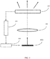
FIG. 3 is a schematic diagram of light emission control for a light source in a mobile terminal according to an embodiment of this disclosure. - The following clearly and completely describes the technical solutions in the embodiments of this disclosure with reference to the accompanying drawings in the embodiments of this disclosure. Apparently, the described embodiments are some rather than all of the embodiments of this disclosure. All other embodiments obtained by a person of ordinary skill in the art based on the embodiments of this disclosure without creative efforts shall fall within the protection scope of this disclosure.
- Unless otherwise defined, the technical terms or scientific terms used in this disclosure should have general meanings understood by a person of ordinary skill in the field to which this disclosure pertains. "First", "second", and like words used in this disclosure do not indicate any order, quantity, or importance, but are merely used to distinguish between different components. Similarly, "a" or "an" or like words do not indicate a quantitative limitation, but indicate at least one. "Connect" or "connected" or like words are not limited to a physical or mechanical connection, but may include an electrical connection, whether direct or indirect. "Up", "down", "left", "right", and the like are merely used to indicate a relative positional relationship, and the relative positional relationship changes accordingly when an absolute position of the described object changes.
- With reference to
FIG. 1 to FIG. 3 , an embodiment of this disclosure provides a light module, including: - a
support body 101, where thesupport body 101 has alight path channel 1011; - a
substrate 102, where thesubstrate 102 is connected to thesupport body 101 and is located at one end of thelight path channel 1011, thesubstrate 102 is provided with alight source 1021, and thelight source 1021 is located in thelight path channel 1011; and - a light-transmitting
element 103, where the light-transmittingelement 103 is connected to thesupport body 101, so as to seal an opening at the other end of thelight path channel 1011, where - a side face of the light-transmitting
element 103 that faces towards thelight source 1021 is provided with a firstelectrical contact point 1031, a secondelectrical contact point 1032, and aphotosensitive coating 1033 capable of converting light energy of the light source into electrical energy, the firstelectrical contact point 1031 and the secondelectrical contact point 1032 are electrically connected by means of thephotosensitive coating 1033, and the firstelectrical contact point 1031 and the secondelectrical contact point 1032 are configured to connect to adetection module 104, so that thedetection module 104 detects a value of a voltage across the firstelectrical contact point 1031 and the secondelectrical contact point 1032. - It should be noted that in an optional embodiment, the foregoing detection module may be provided on the
foregoing substrate 102; in another optional embodiment, the foregoing detection module may alternatively be an external detection module, and the external detection module is a component in a mobile terminal other than the light module, for example, may be a part of a circuit of a main board of the mobile terminal, which is not further limited herein. - The foregoing light module may be applied in different scenarios. In this embodiment, the foregoing light module may be a floodlight module. A structure of the foregoing
light source 1021 may be set based on actual requirements. For example, thelight source 1021 may be a laser chip or a light-emitting diode. The laser chip may be a vertical-cavity surface-emitting laser (Vertical Cavity Surface Emitting Laser, VCSEL) or a laser diode (Laser Diode, LD). The light-emitting diode may be an infrared LED. In the following embodiments, a detailed description is provided by using an example in which thelight source 1021 is a vertical-cavity surface-emitting laser. - The
foregoing substrate 102 may be a substrate for packaging the vertical-cavity surface-emitting laser. The substrate is provided with a circuit structure inside and may be electrically connected to thelight source 1021. Thelight source 1021 may be connected to adriver module 105 by means of thesubstrate 102, and light emission of the light source is controlled by thedriver module 105. - The
foregoing support body 101 may be a hollow structure having openings at both ends, and the hollow part forms thelight path channel 1011. Specifically, a shape of thesupport body 101 may be set based on actual requirements, as long as thesupport body 101 can support the light-transmittingelement 103. - In this embodiment of this disclosure, the
foregoing support body 101 may be fixedly bonded to the light-transmittingelement 103. A connection relationship between theforegoing support body 101 and thesubstrate 102 may be set based on actual requirements. For example, in an optional embodiment, thesupport body 101 and thesubstrate 102 may be integrally formed. In other embodiments, an adhesive may alternatively be provided for fixed bonding. - Specifically, during normal use, the driver module may control the
light source 1021 to emit light. Light rays from thelight source 1021 are incident on a surface of the light-transmittingelement 103 through thelight path channel 1011, and then enter the outside after passing through the light-transmittingelement 103. In this case, theforegoing detection module 104 may detect that the firstelectrical contact point 1031 and the secondelectrical contact point 1032 are electrically connected by means of thephotosensitive coating 1033. When the light-transmittingelement 103 breaks or falls off, thedetection module 104 detects that the electrical connection between the firstelectrical contact point 1031 and the secondelectrical contact point 1032 is disconnected, with a voltage being 0. When the light-transmittingelement 103 shifts, an area of thephotosensitive coating 1033 in the light path channel 101 changes, and thedetection module 104 detects that a voltage across the firstelectrical contact point 1031 and the secondelectrical contact point 1032 increases or decreases. In this case, thedetection module 104 may output a control signal to thedriver module 105, to control thedetection module 104 to turn off thelight source 1021, such that thelight source 1021 stops emitting light. In this way, direct emission of light rays from thelight source 1021 can be avoided, thereby improving use safety of the light module. - In this embodiment of this disclosure, the
photosensitive coating 1033 is provided on the light-transmittingelement 103 so as to connect to the firstelectrical contact point 1031 and the secondelectrical contact point 1032, and when the light-transmittingelement 103 breaks, falls off, or shifts, thedetection module 104 detects an abnormal voltage across the firstelectrical contact point 1031 and the secondelectrical contact point 1032, and thedriver module 105 controls the light source to stop emitting light, thereby effectively avoiding direct emission of light rays from thelight source 1021. Therefore, the light module provided in the embodiments of this disclosure improves use safety of the light module. - A position of the foregoing photosensitive coating may be set based on actual requirements. For example, in an optional embodiment, at least part of the region of the photosensitive coating is located in the
light path channel 1011. - In this way, the part of the photosensitive coating that is in the
light path channel 1011 may be radiated by the light source, so that light energy can be converted into electrical energy, and a voltage across the firstelectrical contact point 1031 and the secondelectrical contact point 1032 is generated. In this embodiment, whether the light-transmittingelement 103 is intact may be determined by monitoring, by thedetection module 104, an electrical signal between the firstelectrical contact point 1031 and the secondelectrical contact point 1032. For example, in this embodiment, the foregoing detection module may be implemented by including a resistor and a control chip. Two ends of the resistor may be directly connected between the firstelectrical contact point 1031 and the secondelectrical contact point 1032. The control chip may perform detection for a voltage across the two ends of the resistor. When thelight source 1021 is in a light emitting state, if thedetection module 104 detects that the voltage is 0, it may be determined that the light-transmittingelement 103 is damaged. Certainly, in other embodiments, other detection methods may alternatively be used for detection, and are not described herein one by one. - It should be noted that the foregoing
detection module 104 and thedriver module 105 may be designed based on dimension requirements of the light module. For example, in an optional embodiment, thedetection module 104 and thedriver module 105 may be arranged inside the light module. In another optional embodiment, thedetection module 104 and thedriver module 105 may alternatively be arranged outside the light module, or may be arranged near the light module. - Specifically, a manner in which the first
electrical contact point 1031 and the secondelectrical contact point 1032 are connected to thedetection module 104 may be set based on actual requirements. For example, in this embodiment, the foregoing light module further includes a first conducting wire and a second conducting wire, where one end of the first conducting wire is connected to the first electrical contact point, and the other end of the first conducting wire is electrically connected to the detection module; and one end of the second conducting wire is connected to the second electrical contact point, and the other end of the second conducting wire is electrically connected to the detection module. - In an optional embodiment, the first conducting wire and the second conducting wire may be provided on the
support body 101. Specifically, the first conducting wire forms a first electrical connection point at an end of thesupport body 101 that faces towards the light-transmittingelement 103, and the first electrical connection point is electrically connected to the first electrical contact point; and the second conducting wire forms a second electrical connection point at the end of thesupport body 101 that faces towards the light-transmittingelement 103, and the second electrical connection point is electrically connected to the second electrical contact point. - In this embodiment, parts of the first conducting wire and the second conducting wire other than the first electrical connection point and the second electrical connection point may be provided on inner and outer surfaces of a side wall of the
support body 101, or may be provided inside a side wall of thesupport body 101, which is not further limited herein. In this embodiment, the first electrical contact point and the second electrical contact point are electrically connected to the substrate by means of the first conducting wire and the second conducting wire, respectively, and then are electrically connected to thedetection module 104 by means of the substrate. Because the first conducting wire and the second conducting wire are provided on thesupport body 101, the electrical connection between the firstelectrical contact point 1031 and the secondelectrical contact point 1032, and thedetection module 104 is implemented, which is simple in structure and easy to mount. - Further, based on the foregoing embodiment, in this embodiment, a region that corresponds to the
light path channel 1011 and that is on the side face of the light-transmittingelement 103 that faces towards the light source is a light-transmitting region, the light-transmitting region is provided with anoptical structure region 1034 and at least part of the region of thephotosensitive coating 1033, and thephotosensitive coating 1033 and theoptical structure region 1034 do not overlap. - The foregoing
optical structure region 1034 is usually provided with a specific optical structure for diffusing a small-angle laser beam emitted by the laser chip, into a uniform large-angle light surface or spot, that is, the optical structure region functions to diverge a light beam. A laser originally having good directivity and concentrated energy has reduced energy density after being diffused by the light-transmitting element, making the light module a product that meets safety specifications. Specifically, a size and structure of theoptical structure region 1034 may be set based on actual requirements, which is not further limited herein. - It should be noted that a shape of the
photosensitive coating 1033 may be set based on actual requirements. As shown inFIG. 2 , in this embodiment, thephotosensitive coating 1033 is provided in a strip shape. Specifically, in an optional embodiment, the firstelectrical contact point 1031 and the secondelectrical contact point 1032 are located on a same side of theoptical structure region 1034, and thephotosensitive coating 1033 is provided around theoptical structure region 1034. - In
FIG. 2 , the foregoingphotosensitive coating 1033 is provided substantially in a "C" shape. In this way, theoptical structure region 1034 is not affected, and in addition, comprehensiveness of checking whether the light-transmittingelement 103 is broken can be improved. - Moreover, the first electrical connection point and the second electrical connection point may be metal connecting sheets. To improve contact reliability, the metal connecting sheets may be provided to be elastically connected to the
support body 101, such that after the light-transmittingelement 103 is mounted and fixed, the metal connecting sheets can abut against the respective electrical contact points, thereby implementing the electrical connection. - Further, based on the foregoing embodiment, in this embodiment, the first
electrical contact point 1031 and the secondelectrical contact point 1032 are both metal conducting plates. - The metal conducting plate may be provided as a square plate, and a side length of the metal conducting plate may be greater than a width of the
photosensitive coating 1033, so as to facilitate contact with the first electrical connection point and the second electrical connection point. - It should be noted that to improve a light emitting effect of a light ray, in this embodiment, a
collimating element 106 may further be provided in the foregoinglight path channel 1011. Thecollimating element 106 is a lens that can convert incident light rays into substantially parallel emergent light rays. In this way, uniformity of light from the light module can be improved. - Further, an embodiment of this disclosure further provides a mobile terminal, and the mobile terminal includes the foregoing light module, a detection module, and a driver module configured to control light emission of the light source of the light module, where
- the detection module is electrically connected to the first electrical contact point and the second electrical contact point in the light module; and
- the driver module is electrically connected to the detection module.
- In this embodiment, for implementation of structures and functions of the foregoing light module, the detection module, and the driver module, reference may be made to the foregoing embodiment, and details are not described herein again. Because the light module in the foregoing embodiment is used, the mobile terminal provided in this embodiment of this disclosure has all the beneficial effects of the foregoing light module.
- The foregoing descriptions are merely embodiments of this disclosure, but the protection scope of this disclosure is not limited thereto. Any variation or replacement readily figured out by a person skilled in the art within the technical scope disclosed in this disclosure shall fall within the protection scope of this disclosure. Therefore, the protection scope of this disclosure shall be subject to the protection scope of the claims.
Claims (10)
- A light module, comprising:a support body, wherein the support body has a light path channel;a substrate, wherein the substrate is connected to the support body and is located at one end of the light path channel, the substrate is provided with a light source, and the light source is located in the light path channel; anda light-transmitting element, wherein the light-transmitting element is connected to the support body, so as to seal an opening at the other end of the light path channel; whereina side face of the light-transmitting element that faces towards the light source is provided with a first electrical contact point, a second electrical contact point, and a photosensitive coating capable of converting light energy of the light source into electrical energy, the first electrical contact point and the second electrical contact point are electrically connected by the photosensitive coating, and the first electrical contact point and the second electrical contact point are configured to connect to a detection module, so that the detection module detects a value of a voltage across the first electrical contact point and the second electrical contact point.
- The light module according to claim 1, wherein the detection module is provided on the substrate, or the detection module is an external detection module.
- The light module according to claim 1, wherein the photosensitive coating is at least partially located in the light path channel.
- The light module according to claim 1, further comprising a first conducting wire and a second conducting wire, wherein one end of the first conducting wire is connected to the first electrical contact point, and the other end of the first conducting wire is electrically connected to the detection module; and one end of the second conducting wire is connected to the second electrical contact point, and the other end of the second conducting wire is electrically connected to the detection module.
- The light module according to claim 4, wherein the first conducting wire and the second conducting wire are provided on the support body, wherein the first conducting wire forms a first electrical connection point at an end of the support body that faces towards the light-transmitting element, and the first electrical connection point is electrically connected to the first electrical contact point; and the second conducting wire forms a second electrical connection point at the end of the support body that faces towards the light-transmitting element, and the second electrical connection point is electrically connected to the second electrical contact point.
- The light module according to claim 1, wherein a region that corresponds to the light path channel and that is on the side face of the light-transmitting element that faces towards the light source is a light-transmitting region, the light-transmitting region is provided with an optical structure region and at least part of the region of the photosensitive coating, and the photosensitive coating and the optical structure region do not overlap.
- The light module according to claim 6, wherein the photosensitive coating is provided in a strip shape.
- The light module according to claim 7, wherein the first electrical contact point and the second electrical contact point are located on a same side of the optical structure region, and the photosensitive coating is provided around the optical structure region.
- The light module according to any one of claims 1 to 8, wherein the light source is a laser chip or a light-emitting diode.
- A mobile terminal, comprising the light module according to any one of claims 1 to 9, a detection module, and a driver module configured to control light emission of the light source of the light module, whereinthe detection module is electrically connected to the first electrical contact point and the second electrical contact point in the light module; andthe driver module is electrically connected to the detection module.
Applications Claiming Priority (2)
| Application Number | Priority Date | Filing Date | Title |
|---|---|---|---|
| CN201910172883.7A CN109751521B (en) | 2019-03-07 | 2019-03-07 | Light module and mobile terminal |
| PCT/CN2020/077739 WO2020177710A1 (en) | 2019-03-07 | 2020-03-04 | Light module and mobile terminal |
Publications (3)
| Publication Number | Publication Date |
|---|---|
| EP3936755A1 true EP3936755A1 (en) | 2022-01-12 |
| EP3936755A4 EP3936755A4 (en) | 2022-05-04 |
| EP3936755B1 EP3936755B1 (en) | 2025-04-23 |
Family
ID=66408220
Family Applications (1)
| Application Number | Title | Priority Date | Filing Date |
|---|---|---|---|
| EP20766256.0A Active EP3936755B1 (en) | 2019-03-07 | 2020-03-04 | Light module and mobile terminal |
Country Status (6)
| Country | Link |
|---|---|
| US (1) | US11448387B2 (en) |
| EP (1) | EP3936755B1 (en) |
| JP (1) | JP7482888B2 (en) |
| CN (1) | CN109751521B (en) |
| ES (1) | ES3028872T3 (en) |
| WO (1) | WO2020177710A1 (en) |
Families Citing this family (5)
| Publication number | Priority date | Publication date | Assignee | Title |
|---|---|---|---|---|
| CN109751521B (en) | 2019-03-07 | 2020-07-28 | 维沃移动通信有限公司 | Light module and mobile terminal |
| US12212119B2 (en) * | 2020-04-23 | 2025-01-28 | Analog Devices International Unlimited Company | Laser system |
| FR3116382B1 (en) * | 2020-11-16 | 2023-04-28 | St Microelectronics Grenoble 2 | Package for integrated circuit and manufacturing method |
| US11396994B1 (en) * | 2021-02-16 | 2022-07-26 | Ii-Vi Delaware, Inc. | Laser light source having diffuser element and light diverging optic |
| WO2024175362A1 (en) * | 2023-02-22 | 2024-08-29 | Ams International Ag | Optical component with damage detection element |
Family Cites Families (34)
| Publication number | Priority date | Publication date | Assignee | Title |
|---|---|---|---|---|
| JPH03216635A (en) * | 1990-01-23 | 1991-09-24 | Pioneer Electron Corp | Projection screen |
| JP2535659B2 (en) * | 1990-09-10 | 1996-09-18 | 三田工業株式会社 | Light / heat sensor |
| JP2970654B1 (en) * | 1998-05-22 | 1999-11-02 | 日新電機株式会社 | Thin film forming equipment |
| JP3120112B2 (en) * | 1998-12-01 | 2000-12-25 | 科学技術庁金属材料技術研究所長 | Precise placement of small objects |
| US7569802B1 (en) * | 2003-03-20 | 2009-08-04 | Patrick Mullins | Photosensor control unit for a lighting module |
| TWM311892U (en) * | 2006-11-22 | 2007-05-11 | Lite On Semiconductor Corp | Movable inspection detecting module |
| EP2489244B1 (en) * | 2009-10-14 | 2019-07-03 | Hewlett-Packard Development Company, L.P. | Stabilized light source having luminance feedback control |
| JP5781838B2 (en) * | 2010-08-25 | 2015-09-24 | スタンレー電気株式会社 | Light source device and lamp for vehicle |
| US20130044444A1 (en) * | 2011-08-18 | 2013-02-21 | General Electric Company | System assembly and design of photoelectric controller device |
| US8480246B2 (en) * | 2011-06-10 | 2013-07-09 | Rockwell Automation Technologies, Inc. | System and method for reduction of optical noise |
| PL224044B1 (en) * | 2011-07-13 | 2016-11-30 | Doros Teodora D A Glass | Method for obtaining a homogeneous beam of electromagnetic radiation of any geometrical shape and the mechanical-optical device to apply this method |
| DE102015213460A1 (en) * | 2015-07-17 | 2017-01-19 | Osram Gmbh | Wavelength conversion of primary light by means of a conversion body |
| US9776560B1 (en) * | 2016-03-23 | 2017-10-03 | Nissan North America, Inc. | Vehicle component including a lighting system |
| US10368411B2 (en) * | 2016-09-20 | 2019-07-30 | Bolb Inc. | Ultraviolet light module having output power control mechanism |
| CN107608167A (en) * | 2017-10-11 | 2018-01-19 | 深圳奥比中光科技有限公司 | Laser projection device and its method of controlling security |
| CN207456385U (en) * | 2017-11-30 | 2018-06-05 | 深圳奥比中光科技有限公司 | Projection module with Beam Monitoring unit |
| CN107870186A (en) * | 2017-12-18 | 2018-04-03 | 深圳奥比中光科技有限公司 | A kind of optics module containing safety monitoring function |
| CN108333850A (en) * | 2018-02-27 | 2018-07-27 | 广东欧珀移动通信有限公司 | Laser projection module and its damage detection method, depth camera and electronic device |
| CN108388072B (en) * | 2018-02-27 | 2020-01-10 | Oppo广东移动通信有限公司 | Laser projection module, depth camera and electronic device |
| CN112611546A (en) * | 2018-02-27 | 2021-04-06 | Oppo广东移动通信有限公司 | Laser projection module, depth camera and electronic device |
| CN108490572B (en) * | 2018-03-12 | 2021-04-23 | Oppo广东移动通信有限公司 | Laser projection modules, depth cameras and electronic devices |
| CN108598849A (en) * | 2018-03-20 | 2018-09-28 | 维沃移动通信有限公司 | Diffusion sheet, laser and mobile device |
| CN108614383A (en) * | 2018-04-03 | 2018-10-02 | Oppo广东移动通信有限公司 | Floodlight assembly, floodlight damage detection method and electronic device |
| CN108832475A (en) * | 2018-04-19 | 2018-11-16 | 信利光电股份有限公司 | Laser emitter and its driving device, driving method and readable storage medium storing program for executing |
| CN108767643A (en) * | 2018-04-19 | 2018-11-06 | 信利光电股份有限公司 | Laser emitter and its driving device, driving method and readable storage medium storing program for executing |
| CN108462774B (en) * | 2018-04-28 | 2019-08-20 | 维沃移动通信有限公司 | A kind of structure optical mode group and mobile terminal |
| CN108879296A (en) * | 2018-06-26 | 2018-11-23 | 维沃移动通信有限公司 | An electronic device and a laser infrared emitting device |
| CN109061879A (en) * | 2018-08-22 | 2018-12-21 | Oppo广东移动通信有限公司 | Light projector, method for detecting breakage of light projector, depth camera, and electronic device |
| CN108828562A (en) * | 2018-08-22 | 2018-11-16 | Oppo广东移动通信有限公司 | Laser projection module, control method, depth image acquisition equipment and electronic device |
| CN208569274U (en) * | 2018-08-23 | 2019-03-01 | 南昌欧菲生物识别技术有限公司 | Projective module group, depth capture device and terminal |
| CN109212763B (en) * | 2018-09-27 | 2020-06-05 | Oppo广东移动通信有限公司 | Light emitting module, damage detection method thereof, depth acquisition device and electronic equipment |
| CN109343227B (en) * | 2018-11-30 | 2021-05-28 | 维沃移动通信(杭州)有限公司 | A light projection module and optical equipment |
| CN109751521B (en) * | 2019-03-07 | 2020-07-28 | 维沃移动通信有限公司 | Light module and mobile terminal |
| US20210038466A1 (en) * | 2019-08-09 | 2021-02-11 | Olympus Innovations, Llc | Cupping device for electrical myofascial decompression |
-
2019
- 2019-03-07 CN CN201910172883.7A patent/CN109751521B/en active Active
-
2020
- 2020-03-04 JP JP2021552657A patent/JP7482888B2/en active Active
- 2020-03-04 EP EP20766256.0A patent/EP3936755B1/en active Active
- 2020-03-04 ES ES20766256T patent/ES3028872T3/en active Active
- 2020-03-04 WO PCT/CN2020/077739 patent/WO2020177710A1/en not_active Ceased
-
2021
- 2021-09-07 US US17/467,824 patent/US11448387B2/en active Active
Also Published As
| Publication number | Publication date |
|---|---|
| JP7482888B2 (en) | 2024-05-14 |
| EP3936755A4 (en) | 2022-05-04 |
| WO2020177710A1 (en) | 2020-09-10 |
| ES3028872T3 (en) | 2025-06-20 |
| EP3936755B1 (en) | 2025-04-23 |
| US11448387B2 (en) | 2022-09-20 |
| CN109751521A (en) | 2019-05-14 |
| CN109751521B (en) | 2020-07-28 |
| US20220026053A1 (en) | 2022-01-27 |
| JP2022523415A (en) | 2022-04-22 |
Similar Documents
| Publication | Publication Date | Title |
|---|---|---|
| US11448387B2 (en) | Light module and mobile terminal | |
| CN110412540B (en) | Light emitting module, time-of-flight camera and electronic device | |
| WO2020038067A1 (en) | Laser projection module and control method therefor, and depth image acquisition apparatus and electronic device | |
| US20170031118A1 (en) | Optoelectronic components housed in a to-can package | |
| SE468027B (en) | OPTION ELECTRONIC COMPONENT WITH SEMICONDUCTOR ELEMENTS INCLUDED IN THE CLOSED CAPSEL, WHICH CAPSELY CONSISTS OF A CAPE WHICH IS CENTERED AND RELATIVELY LOADED A SOCKET BY A BUILDING ELEMENT | |
| US10866375B2 (en) | Light source device and electronic apparatus | |
| WO2020038066A1 (en) | Light projector and method for detecting rupture thereof, and depth camera and electronic device | |
| JP4844031B2 (en) | Light emitting module | |
| CN108387365A (en) | Laser projection module and its damage detection method, depth camera and electronic device | |
| US9525267B2 (en) | Vertical cavity surface emitting laser assembly | |
| JP5068443B2 (en) | Optical coupling device | |
| CN108614383A (en) | Floodlight assembly, floodlight damage detection method and electronic device | |
| JP2007027471A (en) | Semiconductor laser device and light transmitting device using the same | |
| US20230387643A1 (en) | Laser emission module and lidar | |
| CN112393691A (en) | Light emitting module, depth camera and electronic equipment | |
| KR102548859B1 (en) | Beam projector module providing eye protection | |
| US20200285003A1 (en) | Photoelectric conversion module and active optical cable | |
| KR20190142576A (en) | A surface-emitting laser packgae, optical module including the same | |
| KR102246084B1 (en) | Beam projector module providing eye protection | |
| US7324575B2 (en) | Lens with reflective surface | |
| JP4636900B2 (en) | Sensor head for transmissive photoelectric switch | |
| CN222838231U (en) | Packaging structure of optoelectronic device and optical module | |
| CN114628990A (en) | Addressable TOF emission module and laser | |
| CN210582454U (en) | Light Emitting Modules and Imaging Equipment | |
| JP6632650B2 (en) | Optical module |
Legal Events
| Date | Code | Title | Description |
|---|---|---|---|
| STAA | Information on the status of an ep patent application or granted ep patent |
Free format text: STATUS: THE INTERNATIONAL PUBLICATION HAS BEEN MADE |
|
| PUAI | Public reference made under article 153(3) epc to a published international application that has entered the european phase |
Free format text: ORIGINAL CODE: 0009012 |
|
| STAA | Information on the status of an ep patent application or granted ep patent |
Free format text: STATUS: REQUEST FOR EXAMINATION WAS MADE |
|
| 17P | Request for examination filed |
Effective date: 20210930 |
|
| AK | Designated contracting states |
Kind code of ref document: A1 Designated state(s): AL AT BE BG CH CY CZ DE DK EE ES FI FR GB GR HR HU IE IS IT LI LT LU LV MC MK MT NL NO PL PT RO RS SE SI SK SM TR |
|
| A4 | Supplementary search report drawn up and despatched |
Effective date: 20220331 |
|
| RIC1 | Information provided on ipc code assigned before grant |
Ipc: F21V 25/04 20060101ALI20220325BHEP Ipc: F21V 23/04 20060101ALI20220325BHEP Ipc: F21V 3/00 20150101ALI20220325BHEP Ipc: H01S 5/068 20060101ALI20220325BHEP Ipc: H01S 5/02257 20210101ALI20220325BHEP Ipc: H01S 5/00 20060101AFI20220325BHEP |
|
| DAV | Request for validation of the european patent (deleted) | ||
| DAX | Request for extension of the european patent (deleted) | ||
| REG | Reference to a national code |
Ref legal event code: R079 Ipc: H01S0005000000 Ref country code: DE Ref legal event code: R079 Ref document number: 602020049997 Country of ref document: DE Free format text: PREVIOUS MAIN CLASS: F21K0009238000 Ipc: H01S0005000000 |
|
| GRAP | Despatch of communication of intention to grant a patent |
Free format text: ORIGINAL CODE: EPIDOSNIGR1 |
|
| STAA | Information on the status of an ep patent application or granted ep patent |
Free format text: STATUS: GRANT OF PATENT IS INTENDED |
|
| RIC1 | Information provided on ipc code assigned before grant |
Ipc: F21V 23/00 20150101ALI20241115BHEP Ipc: F21V 3/00 20150101ALI20241115BHEP Ipc: F21V 23/04 20060101ALI20241115BHEP Ipc: F21V 25/04 20060101ALI20241115BHEP Ipc: H01S 5/068 20060101ALI20241115BHEP Ipc: H01S 5/02257 20210101ALI20241115BHEP Ipc: H01S 5/00 20060101AFI20241115BHEP |
|
| INTG | Intention to grant announced |
Effective date: 20241205 |
|
| GRAS | Grant fee paid |
Free format text: ORIGINAL CODE: EPIDOSNIGR3 |
|
| GRAA | (expected) grant |
Free format text: ORIGINAL CODE: 0009210 |
|
| STAA | Information on the status of an ep patent application or granted ep patent |
Free format text: STATUS: THE PATENT HAS BEEN GRANTED |
|
| AK | Designated contracting states |
Kind code of ref document: B1 Designated state(s): AL AT BE BG CH CY CZ DE DK EE ES FI FR GB GR HR HU IE IS IT LI LT LU LV MC MK MT NL NO PL PT RO RS SE SI SK SM TR |
|
| REG | Reference to a national code |
Ref country code: GB Ref legal event code: FG4D |
|
| REG | Reference to a national code |
Ref country code: CH Ref legal event code: EP |
|
| REG | Reference to a national code |
Ref country code: DE Ref legal event code: R096 Ref document number: 602020049997 Country of ref document: DE |
|
| REG | Reference to a national code |
Ref country code: IE Ref legal event code: FG4D |
|
| REG | Reference to a national code |
Ref country code: NL Ref legal event code: FP |
|
| REG | Reference to a national code |
Ref country code: ES Ref legal event code: FG2A Ref document number: 3028872 Country of ref document: ES Kind code of ref document: T3 Effective date: 20250620 |
|
| REG | Reference to a national code |
Ref country code: AT Ref legal event code: MK05 Ref document number: 1788754 Country of ref document: AT Kind code of ref document: T Effective date: 20250423 |
|
| PG25 | Lapsed in a contracting state [announced via postgrant information from national office to epo] |
Ref country code: FI Free format text: LAPSE BECAUSE OF FAILURE TO SUBMIT A TRANSLATION OF THE DESCRIPTION OR TO PAY THE FEE WITHIN THE PRESCRIBED TIME-LIMIT Effective date: 20250423 Ref country code: PT Free format text: LAPSE BECAUSE OF FAILURE TO SUBMIT A TRANSLATION OF THE DESCRIPTION OR TO PAY THE FEE WITHIN THE PRESCRIBED TIME-LIMIT Effective date: 20250825 |
|
| REG | Reference to a national code |
Ref country code: LT Ref legal event code: MG9D |
|
| PG25 | Lapsed in a contracting state [announced via postgrant information from national office to epo] |
Ref country code: NO Free format text: LAPSE BECAUSE OF FAILURE TO SUBMIT A TRANSLATION OF THE DESCRIPTION OR TO PAY THE FEE WITHIN THE PRESCRIBED TIME-LIMIT Effective date: 20250723 Ref country code: GR Free format text: LAPSE BECAUSE OF FAILURE TO SUBMIT A TRANSLATION OF THE DESCRIPTION OR TO PAY THE FEE WITHIN THE PRESCRIBED TIME-LIMIT Effective date: 20250724 |
|
| PG25 | Lapsed in a contracting state [announced via postgrant information from national office to epo] |
Ref country code: PL Free format text: LAPSE BECAUSE OF FAILURE TO SUBMIT A TRANSLATION OF THE DESCRIPTION OR TO PAY THE FEE WITHIN THE PRESCRIBED TIME-LIMIT Effective date: 20250423 |
|
| PG25 | Lapsed in a contracting state [announced via postgrant information from national office to epo] |
Ref country code: BG Free format text: LAPSE BECAUSE OF FAILURE TO SUBMIT A TRANSLATION OF THE DESCRIPTION OR TO PAY THE FEE WITHIN THE PRESCRIBED TIME-LIMIT Effective date: 20250423 |
|
| PG25 | Lapsed in a contracting state [announced via postgrant information from national office to epo] |
Ref country code: HR Free format text: LAPSE BECAUSE OF FAILURE TO SUBMIT A TRANSLATION OF THE DESCRIPTION OR TO PAY THE FEE WITHIN THE PRESCRIBED TIME-LIMIT Effective date: 20250423 |
|
| PG25 | Lapsed in a contracting state [announced via postgrant information from national office to epo] |
Ref country code: AT Free format text: LAPSE BECAUSE OF FAILURE TO SUBMIT A TRANSLATION OF THE DESCRIPTION OR TO PAY THE FEE WITHIN THE PRESCRIBED TIME-LIMIT Effective date: 20250423 |
|
| PG25 | Lapsed in a contracting state [announced via postgrant information from national office to epo] |
Ref country code: RS Free format text: LAPSE BECAUSE OF FAILURE TO SUBMIT A TRANSLATION OF THE DESCRIPTION OR TO PAY THE FEE WITHIN THE PRESCRIBED TIME-LIMIT Effective date: 20250723 |
|
| PG25 | Lapsed in a contracting state [announced via postgrant information from national office to epo] |
Ref country code: IS Free format text: LAPSE BECAUSE OF FAILURE TO SUBMIT A TRANSLATION OF THE DESCRIPTION OR TO PAY THE FEE WITHIN THE PRESCRIBED TIME-LIMIT Effective date: 20250823 |
|
| PG25 | Lapsed in a contracting state [announced via postgrant information from national office to epo] |
Ref country code: LV Free format text: LAPSE BECAUSE OF FAILURE TO SUBMIT A TRANSLATION OF THE DESCRIPTION OR TO PAY THE FEE WITHIN THE PRESCRIBED TIME-LIMIT Effective date: 20250423 |
|
| PG25 | Lapsed in a contracting state [announced via postgrant information from national office to epo] |
Ref country code: DK Free format text: LAPSE BECAUSE OF FAILURE TO SUBMIT A TRANSLATION OF THE DESCRIPTION OR TO PAY THE FEE WITHIN THE PRESCRIBED TIME-LIMIT Effective date: 20250423 Ref country code: SM Free format text: LAPSE BECAUSE OF FAILURE TO SUBMIT A TRANSLATION OF THE DESCRIPTION OR TO PAY THE FEE WITHIN THE PRESCRIBED TIME-LIMIT Effective date: 20250423 |
|
| PG25 | Lapsed in a contracting state [announced via postgrant information from national office to epo] |
Ref country code: CZ Free format text: LAPSE BECAUSE OF FAILURE TO SUBMIT A TRANSLATION OF THE DESCRIPTION OR TO PAY THE FEE WITHIN THE PRESCRIBED TIME-LIMIT Effective date: 20250423 |
|
| PG25 | Lapsed in a contracting state [announced via postgrant information from national office to epo] |
Ref country code: EE Free format text: LAPSE BECAUSE OF FAILURE TO SUBMIT A TRANSLATION OF THE DESCRIPTION OR TO PAY THE FEE WITHIN THE PRESCRIBED TIME-LIMIT Effective date: 20250423 |
|
| REG | Reference to a national code |
Ref country code: DE Ref legal event code: R097 Ref document number: 602020049997 Country of ref document: DE |
|
| PG25 | Lapsed in a contracting state [announced via postgrant information from national office to epo] |
Ref country code: SK Free format text: LAPSE BECAUSE OF FAILURE TO SUBMIT A TRANSLATION OF THE DESCRIPTION OR TO PAY THE FEE WITHIN THE PRESCRIBED TIME-LIMIT Effective date: 20250423 Ref country code: RO Free format text: LAPSE BECAUSE OF FAILURE TO SUBMIT A TRANSLATION OF THE DESCRIPTION OR TO PAY THE FEE WITHIN THE PRESCRIBED TIME-LIMIT Effective date: 20250423 |
|
| PLBE | No opposition filed within time limit |
Free format text: ORIGINAL CODE: 0009261 |
|
| STAA | Information on the status of an ep patent application or granted ep patent |
Free format text: STATUS: NO OPPOSITION FILED WITHIN TIME LIMIT |
|
| REG | Reference to a national code |
Ref country code: CH Ref legal event code: L10 Free format text: ST27 STATUS EVENT CODE: U-0-0-L10-L00 (AS PROVIDED BY THE NATIONAL OFFICE) Effective date: 20260304 |
|
| PGFP | Annual fee paid to national office [announced via postgrant information from national office to epo] |
Ref country code: NL Payment date: 20260213 Year of fee payment: 7 |
|
| 26N | No opposition filed |
Effective date: 20260126 |
|
| PGFP | Annual fee paid to national office [announced via postgrant information from national office to epo] |
Ref country code: GB Payment date: 20260202 Year of fee payment: 7 |
|
| PGFP | Annual fee paid to national office [announced via postgrant information from national office to epo] |
Ref country code: DE Payment date: 20260128 Year of fee payment: 7 |
|
| PGFP | Annual fee paid to national office [announced via postgrant information from national office to epo] |
Ref country code: IT Payment date: 20260220 Year of fee payment: 7 |
|
| PGFP | Annual fee paid to national office [announced via postgrant information from national office to epo] |
Ref country code: FR Payment date: 20260209 Year of fee payment: 7 |