EP3933910A1 - Package substrate and forming method therefor, and package structure and forming method therefor - Google Patents
Package substrate and forming method therefor, and package structure and forming method therefor Download PDFInfo
- Publication number
- EP3933910A1 EP3933910A1 EP20919808.4A EP20919808A EP3933910A1 EP 3933910 A1 EP3933910 A1 EP 3933910A1 EP 20919808 A EP20919808 A EP 20919808A EP 3933910 A1 EP3933910 A1 EP 3933910A1
- Authority
- EP
- European Patent Office
- Prior art keywords
- substrate
- vent hole
- chip
- package substrate
- hole
- Prior art date
- Legal status (The legal status is an assumption and is not a legal conclusion. Google has not performed a legal analysis and makes no representation as to the accuracy of the status listed.)
- Granted
Links
Images



Classifications
-
- H—ELECTRICITY
- H10—SEMICONDUCTOR DEVICES; ELECTRIC SOLID-STATE DEVICES NOT OTHERWISE PROVIDED FOR
- H10W—GENERIC PACKAGES, INTERCONNECTIONS, CONNECTORS OR OTHER CONSTRUCTIONAL DETAILS OF DEVICES COVERED BY CLASS H10
- H10W74/00—Encapsulations, e.g. protective coatings
- H10W74/01—Manufacture or treatment
- H10W74/016—Manufacture or treatment using moulds
-
- H—ELECTRICITY
- H10—SEMICONDUCTOR DEVICES; ELECTRIC SOLID-STATE DEVICES NOT OTHERWISE PROVIDED FOR
- H10W—GENERIC PACKAGES, INTERCONNECTIONS, CONNECTORS OR OTHER CONSTRUCTIONAL DETAILS OF DEVICES COVERED BY CLASS H10
- H10W70/00—Package substrates; Interposers; Redistribution layers [RDL]
- H10W70/60—Insulating or insulated package substrates; Interposers; Redistribution layers
- H10W70/67—Insulating or insulated package substrates; Interposers; Redistribution layers characterised by their insulating layers or insulating parts
- H10W70/68—Shapes or dispositions thereof
-
- H—ELECTRICITY
- H10—SEMICONDUCTOR DEVICES; ELECTRIC SOLID-STATE DEVICES NOT OTHERWISE PROVIDED FOR
- H10W—GENERIC PACKAGES, INTERCONNECTIONS, CONNECTORS OR OTHER CONSTRUCTIONAL DETAILS OF DEVICES COVERED BY CLASS H10
- H10W74/00—Encapsulations, e.g. protective coatings
- H10W74/01—Manufacture or treatment
- H10W74/012—Manufacture or treatment of encapsulations on active surfaces of flip-chip devices, e.g. forming underfills
-
- H—ELECTRICITY
- H10—SEMICONDUCTOR DEVICES; ELECTRIC SOLID-STATE DEVICES NOT OTHERWISE PROVIDED FOR
- H10W—GENERIC PACKAGES, INTERCONNECTIONS, CONNECTORS OR OTHER CONSTRUCTIONAL DETAILS OF DEVICES COVERED BY CLASS H10
- H10W74/00—Encapsulations, e.g. protective coatings
- H10W74/10—Encapsulations, e.g. protective coatings characterised by their shape or disposition
- H10W74/111—Encapsulations, e.g. protective coatings characterised by their shape or disposition the semiconductor body being completely enclosed
- H10W74/114—Encapsulations, e.g. protective coatings characterised by their shape or disposition the semiconductor body being completely enclosed by a substrate and the encapsulations
-
- H—ELECTRICITY
- H10—SEMICONDUCTOR DEVICES; ELECTRIC SOLID-STATE DEVICES NOT OTHERWISE PROVIDED FOR
- H10W—GENERIC PACKAGES, INTERCONNECTIONS, CONNECTORS OR OTHER CONSTRUCTIONAL DETAILS OF DEVICES COVERED BY CLASS H10
- H10W74/00—Encapsulations, e.g. protective coatings
- H10W74/10—Encapsulations, e.g. protective coatings characterised by their shape or disposition
- H10W74/111—Encapsulations, e.g. protective coatings characterised by their shape or disposition the semiconductor body being completely enclosed
- H10W74/114—Encapsulations, e.g. protective coatings characterised by their shape or disposition the semiconductor body being completely enclosed by a substrate and the encapsulations
- H10W74/117—Encapsulations, e.g. protective coatings characterised by their shape or disposition the semiconductor body being completely enclosed by a substrate and the encapsulations the substrate having spherical bumps for external connection
-
- H—ELECTRICITY
- H10—SEMICONDUCTOR DEVICES; ELECTRIC SOLID-STATE DEVICES NOT OTHERWISE PROVIDED FOR
- H10W—GENERIC PACKAGES, INTERCONNECTIONS, CONNECTORS OR OTHER CONSTRUCTIONAL DETAILS OF DEVICES COVERED BY CLASS H10
- H10W74/00—Encapsulations, e.g. protective coatings
- H10W74/10—Encapsulations, e.g. protective coatings characterised by their shape or disposition
- H10W74/111—Encapsulations, e.g. protective coatings characterised by their shape or disposition the semiconductor body being completely enclosed
- H10W74/127—Encapsulations, e.g. protective coatings characterised by their shape or disposition the semiconductor body being completely enclosed characterised by arrangements for sealing or adhesion
-
- H—ELECTRICITY
- H10—SEMICONDUCTOR DEVICES; ELECTRIC SOLID-STATE DEVICES NOT OTHERWISE PROVIDED FOR
- H10W—GENERIC PACKAGES, INTERCONNECTIONS, CONNECTORS OR OTHER CONSTRUCTIONAL DETAILS OF DEVICES COVERED BY CLASS H10
- H10W74/00—Encapsulations, e.g. protective coatings
- H10W74/10—Encapsulations, e.g. protective coatings characterised by their shape or disposition
- H10W74/15—Encapsulations, e.g. protective coatings characterised by their shape or disposition on active surfaces of flip-chip devices, e.g. underfills
-
- H—ELECTRICITY
- H10—SEMICONDUCTOR DEVICES; ELECTRIC SOLID-STATE DEVICES NOT OTHERWISE PROVIDED FOR
- H10W—GENERIC PACKAGES, INTERCONNECTIONS, CONNECTORS OR OTHER CONSTRUCTIONAL DETAILS OF DEVICES COVERED BY CLASS H10
- H10W99/00—Subject matter not provided for in other groups of this subclass
-
- H—ELECTRICITY
- H10—SEMICONDUCTOR DEVICES; ELECTRIC SOLID-STATE DEVICES NOT OTHERWISE PROVIDED FOR
- H10W—GENERIC PACKAGES, INTERCONNECTIONS, CONNECTORS OR OTHER CONSTRUCTIONAL DETAILS OF DEVICES COVERED BY CLASS H10
- H10W70/00—Package substrates; Interposers; Redistribution layers [RDL]
- H10W70/60—Insulating or insulated package substrates; Interposers; Redistribution layers
- H10W70/67—Insulating or insulated package substrates; Interposers; Redistribution layers characterised by their insulating layers or insulating parts
- H10W70/68—Shapes or dispositions thereof
- H10W70/681—Shapes or dispositions thereof comprising holes not having chips therein, e.g. for outgassing, underfilling or bond wire passage
-
- H—ELECTRICITY
- H10—SEMICONDUCTOR DEVICES; ELECTRIC SOLID-STATE DEVICES NOT OTHERWISE PROVIDED FOR
- H10W—GENERIC PACKAGES, INTERCONNECTIONS, CONNECTORS OR OTHER CONSTRUCTIONAL DETAILS OF DEVICES COVERED BY CLASS H10
- H10W90/00—Package configurations
- H10W90/701—Package configurations characterised by the relative positions of pads or connectors relative to package parts
-
- H—ELECTRICITY
- H10—SEMICONDUCTOR DEVICES; ELECTRIC SOLID-STATE DEVICES NOT OTHERWISE PROVIDED FOR
- H10W—GENERIC PACKAGES, INTERCONNECTIONS, CONNECTORS OR OTHER CONSTRUCTIONAL DETAILS OF DEVICES COVERED BY CLASS H10
- H10W90/00—Package configurations
- H10W90/701—Package configurations characterised by the relative positions of pads or connectors relative to package parts
- H10W90/721—Package configurations characterised by the relative positions of pads or connectors relative to package parts of bump connectors
- H10W90/724—Package configurations characterised by the relative positions of pads or connectors relative to package parts of bump connectors between a chip and a stacked insulating package substrate, interposer or RDL
Definitions
- the present disclosure relates to the field of semiconductor technology, in particular to a package substrate and a method of forming the same, a package structure and a method of forming the same.
- the chip After the chip is packaged, the chip is protected by wrapping the packaged chip through injection molding.
- connections are made between the chip and the substrate through solder balls to connect the chip to circuits on the substrate.
- the molding process requires a mold compound to wrap the entire chip, filling the gap between the chip and the substrate. Because the gaps are small and the separation distance between the connection points is small due to direct connection between the chip and the substrate via solder balls or other solder bumps, the mold compound is less prone to air evacuation when filled and is prone to unreliable package structures.
- air holes are provided on the package substrate so that as the mold compound is filled, gas is vented from the air holes on the substrate during injection molding, thereby increasing the filling effect of the mold compound fluid and reducing the phenomena such as unfilled air holes and Wire sweep.
- existing chips are typically designed in non-square dimensions, and a single vent hole tends to achieve the desired effect in the direction of the short side of the chip, whereas in the direction of the long side of the chip it tends to be difficult to achieve the desired effect, there are still more air holes and the mold compound filling effect is poor, affecting the reliability of the product.
- the technical problem underlying the present disclosure is to provide a package substrate and a method of forming the same, a package structure and a method of forming the same, which improve the filling effect of a mold compound during injection molding of a package.
- a package substrate comprising: a substrate having opposing a first surface and a second surface; at least one vent hole extending through the first surface and the second surface of the substrate, the vent hole comprising at least a long-strip hole.
- the vent hole comprises two or more of the cross-connected long-strip holes.
- the package substrate comprises more than two of the vent holes uniformly distributed in a length direction of the package substrate.
- vent hole is symmetric about an axis of symmetry of the package substrate.
- a cross-sectional edge of the vent hole parallel to the substrate surface is a smooth line.
- the long-strip hole is formed by connecting a plurality of continuous circular holes.
- the inner wall of the vent hole has a passivation surface.
- the long-strip hole has a width to length ratio ranging from 1: 1.3 to 1:15.
- the package substrate further comprises at least one circular hole distributed across a central axis of the substrate.
- particular embodiments of the present disclosure also provide a method of forming a package substrate, comprises: providing a substrate having a first surface and a second surface; forming at least one vent hole extending through the first surface and the second surface of the substrate, the vent hole including at least a long-strip hole.
- the vent hole comprises two or more of the cross-connected long-strip holes.
- the method of forming a package substrate comprises more than two of the vent holes uniformly distributed in a length direction of the package substrate.
- vent hole is symmetric about an axis of symmetry of the package substrate.
- a cross-sectional edge of the vent hole parallel to the substrate surface is a smooth line.
- the long-strip hole is formed by forming a plurality of continuous circular holes through the substrate, and the plurality of continuous circular holes are interconnected to form the long-strip hole.
- the method of forming a package substrate further comprises performing a passivation process on an inner wall surface of the vent hole.
- the long-strip hole has a width to length ratio ranging from 1: 1.3 to 1:15.
- the method of forming a package substrate further comprises forming at least one circular hole distributed across the central axis of the substrate.
- An aspect of the present disclosure also provides a package structure comprising: a package substrate as described in any of the above; a chip flip-chip fixed to a first surface of the substrate with solder bumps, the vent hole being located within a projection of the chip on the substrate by forming electrical connections between the solder bumps and the substrate; a mold compound enclosing the chip and filling a gap between the chip and the first surface of the substrate and the vent hole.
- An aspect of the present disclosure also provides a method of forming a package structure, comprising: providing a package substrate as described in any of the above; flip-chip fixing a chip to a first surface of the substrate with solder bumps by a flip-chip process, the vent hole within the substrate being located within a projection of the chip on the substrate by forming electrical connections between the solder bumps and the substrate; performing a injection molding process of the chip flip-chip onto the substrate, enclosing the chip and filling a gap between the chip and the first surface of the substrate and the vent holes with a mold compound.
- the packaging substrate of the present disclosure having vent holes extending through the substrate, the vent holes comprising long-strip holes, which can improve the venting effect and reduce the risk of the vent holes becoming blocked during injection molding. Also, while increasing the venting effect, the number of vent holes is reduced so that the soldering region of the substrate to the chip is more concentrated, avoiding wasting design area.
- the inventors have found that in the direction of the long side of the chip, a more pronounced peristaltic flow (Re « 1 in fluid mechanics, or low Reynolds number flow) is generated as the mold compound needs to flow through more solder bump areas, resulting in turbulent influx of the mold compound containing more air bubbles and thus poor venting effect through a single circular hole; This problem can be ameliorated by arranging more air holes in the direction of the long side of the chip, however, more air holes will occupy the area of the soldering region between the chip and the substrate, so that the soldering region is dispersed and design area is wasted.
- hole apertures can be expanded directly to ameliorate problems such as air bubbles and clogging, the solder bumps of the chip and the soldering region of the substrate are also excessively occupied, and the mold compound can droop directly from the hole with large diameter, resulting in unfilled mold compound filling in the area around the hole.
- the inventors propose a new package substrate and a method for forming the same, and a package structure based on the package substrate and a method for forming the same, to solve the above-described problems.
- FIGS. 2a-2c schematic illustrations of a package substrate in accordance with an embodiment of the present disclosure are shown.
- FIG. 2a is a schematic top view of the substrate 200
- FIG. 2b is a schematic cross-sectional view along secant AA 'in FIG. 2a
- FIG. 2c is a schematic cross-sectional view along secant BB' in FIG. 2a .
- the package substrate includes a substrate 200, and a vent hole 210 through the substrate 200.
- the substrate 200 has opposing first surface 201 and second surface 202.
- the substrate 200 may be a circuit board having electrical connection structure like interconnect circuitry, pads, etc. formed on the surface of the substrate 200 and/or within the substrate 200, for making electrical connections to the chip, inputting electrical signals to the chip, or outputting electrical signals generated by the chip.
- the shape of the substrate 200 generally corresponds to the shape of the chip to be packaged, being square or rectangular. In this embodiment, the substrate 200 has a rectangular shape with a length along the Y direction and a width along the X direction.
- the vent hole 210 is a long-strip hole extending through the first surface 201 and the second surface 202 of the substrate 200.
- the region of the first surface 201 of the substrate 200 outside of the vent hole 210 is a soldering region, with a metal connection layer formed for soldering with the chip to be packaged.
- the vent hole 210 includes at least one long-strip hole, and other hole structures in communication with the long-strip hole.
- the vent hole 210 is in the shape of long straight lines, in other embodiments, the vent hole 210 may also be broken line or curved lines, and in particular the vent hole may be shaped according to the distribution of the solder bumps. While increasing the venting effect, by avoiding overly dispersed soldered regions on the substrate 200, the waste of area can be reduced.
- the vent hole 210 When the vent hole 210 has a long-strip shape, the aperture area is larger and the venting effect is better; and, if solid or semi-solid impurities are contained within the mold compound, the impurities are less likely to get stuck within the vent hole with the following of the mold compound, thereby reducing instances of the vent hole 210 becoming blocked. Also, even if the impurities get stuck inside the vent hole 210, gas can be vented from both sides of the impurities because the vent hole 210 has the long-strip shape, thereby preventing the possibility of the vent holes being completely blocked.
- the length direction of the vent hole 210 coincides with the length direction of the substrate 200. Since the mold compound flows a longer distance in the Y-axis direction of the substrate 200 during the injection molding process, more solder bumps are passed through, the vent hole 210 has a longer length in the Y-direction, which can improve the venting effect in the Y-direction. And the vent hole 210 is disposed along the axis of symmetry of the substrate 200, and is symmetric about the axis of symmetry. Since the mold compound typically flows from the edge to the center of the substrate 200 during the injection molding process, the vent hole 210 being provided at the position of axis of symmetry may improve the uniformity of the venting.
- the width to length ratio of the vent hole 210 ranges from 1: 1.3 to 1:15 for a better venting effect.
- the width to length ratio of the vent hole 210 ranges from 1: 2 to 1: 7 to provide a better venting effect and avoid occupying a large substrate area.
- two or more vent holes may also be formed within the substrate 200.
- FIG. 3 a schematic top view of a package substrate in accordance with another embodiment of the present disclosure is shown.
- two vent holes 310 are formed in the substrate 300, each of which is a long-strip hole, the length direction of the vent holes 310 coincides with the length direction of the substrate 300 and the vent holes are distributed along the axis of symmetry.
- FIG. 4a there is a schematic top view of a package substrate in accordance with another embodiment of the present disclosure.
- three vent holes 410 are formed in the substrate 400, the length directions of the vent holes 410 may coincide with the width direction of the substrate 300, and the vent holes are uniformly distributed along the width direction of the substrate 400.
- FIG. 4b there is a schematic top view of a package substrate according to another embodiment wherein two vent holes 420 are arranged obliquely.
- the number and distribution of the vent holes 410, 420 on the substrate 200 can be set properly based on the distribution of the soldering region on the substrate 200 and simulated effects of the flow rate of the mold compound fluid, etc.
- the length to width ratio of the long-strip holes of the vent holes 410, 420 is 1: 1.3 to 1: 15, which has a better effect of venting and avoiding clogging by impurities.
- the substrate may also have at least one circular hole formed through the first surface and the second surface of the substrate.
- the circular holes may be distributed across a central axis of the substrate, preferably, distributed on a central axis along the length direction of the substrate.
- FIG. 5 a schematic top view of a package substrate in accordance with another embodiment of the present disclosure is shown.
- the vent holes 510 in the substrate 500 include two cross-connected long-strip holes 510 and 520, in a crisscross shape.
- the sizes of the hole 501 and the hole 502 are the same, and the length directions of the holes coincide with the length and width directions of the substrate 500, respectively.
- the hole 510 is located at a central position of the substrate 500.
- the sizes of the hole 501 and the hole 502 may also be different, preferably the length of the hole 501 extending along the long side of the substrate 500 is greater than the length of the hole 502 extending along the short side of the substrate 500.
- vent hole may further comprise three or more cross-connected long-strip holes, the cross angles may be perpendicular or oblique to each other, and the cross locations may be located in the middle or in the ends, without being limited here.
- the vent hole 210 has a smooth inner wall edge.
- the cross-sectional edge of the vent hole 210 parallel to the surface of the substrate 200 has smooth lines, and has an arc connect at the position of the corner of the length connecting the width to avoid sharp corner inside the vent hole 210 causing turbulent flow when the gas or fluid passing through, thereby affecting the filling effect of the mold compound.
- the vent hole 210 may be formed by drilling, laser etching, etching, or the like.
- the inner wall surface of the vent hole 210 may also be passivated so that the inner wall surface of the vent hole 210 has a passivation surface to ensure that the vent hole 210 has a smooth inner wall edge.
- the passivation surface may be a passivation layer surface covering the sidewall of the vent hole 210.
- the sidewall of the vent hole 210 is perpendicular to the surface of the substrate 200.
- the vent hole 210 may also have a sloped side wall (please refer to vent hole 210a in Fig. 2d ), or a side wall having a larger middle dimension and two smaller ends (please refer to vent hole 210b in Fig. 2e ), without being limited here.
- FIG. 6 a schematic top view of a package substrate in accordance with an embodiment of the present disclosure is shown.
- the vent hole 610 within the package substrate 600 is formed by connecting a plurality of continuous circular holes 601.
- the size of each of the circular holes 601 is the same, and the size and shape of the vent hole 610 can be adjusted by controlling the number and arrangement of the circular holes 601, and the adjustment is easy to be realized.
- vent hole 610 is connected by circular holes, with a protruding sharp corner where the edges of adjacent circular holes meet, so that the smoothness of the vent hole 610 is to be improved.
- FIG. 7 there is a schematic illustration of a package substrate in accordance with another embodiment of the present disclosure.
- a passivation layer 710 is formed on the inner wall surface of the vent hole 610.
- passivation layer 710 the angle of the protruding sharp corner of the inner wall of the vent hole 610 becomes flat, and the surface of the vent hole 610 becomes arc-shaped, reducing the risk of turbulent flow when the gas or fluid passing through the vent hole 610.
- the passivation layer 710 may be formed by a metallization process.
- the passivation layer 710 may be a metal layer formed by a sputtering process, such as a Cu layer, a W layer, or the like.
- the passivation layer 710 may also be formed on the inner wall surface of the vent hole 610 by chemical deposition.
- the passivation layer 710 may also be formed from other materials that tend to cover the inner wall of the vent hole.
- the inner wall of the vent hole 610 may also be smoothed to remove sharp corners by grinding the inner wall of the vent hole 610, such that there is no sharp protrusion one the inner wall of the vent hole 610.
- the package substrate in the above detailed description having long-strip vent holes, can increase the venting effect and reduce the risk of the vent holes being blocked during injection molding. Also, while increasing the venting effect, the number of vent holes is reduced so that the soldering region between the substrate and the chip is more concentrated, avoiding wasting design area.
- Embodiments of the present disclosure also provide a structural schematic of the above-described formation process of the package substrate.
- a substrate 200 is provided having opposing first surface 201 and second surface 202.
- the substrate 200 may be a circuit board having electrical connection structure like interconnect circuitry, pads, etc. formed on the surface of the substrate 200 and/or within the substrate 200, so that the substrate 200 may be electrically connected to the chip, inputting electrical signals to the chip or outputting electrical signals generated by the chip.
- the shape of the substrate 200 generally corresponds to the shape of the chip to be packaged, being square or rectangular.
- a vent hole 210 is then formed within the substrate 200, extending through the first surface 201 and the second surface 202 of the substrate 200, the vent hole 210 is a long-strip hole.
- the region of the first surface 201 of the substrate 200 outside of the vent hole 210 is a soldering region, with a metal connection layer formed for soldering with the chip to be packaged.
- the vent hole 210 includes at least one long-strip hole, and other hole structures in communication with the long-strip hole.
- the vent hole 210 is in the shape of long straight lines, and in other embodiments, the vent hole 210 may also be broken lines or curved lines. While increasing the venting effect, by avoiding overly dispersed the soldering regions on the substrate 200, the waste of area can be reduced.
- the length direction of the vent hole 210 coincides with the length direction of the substrate 200. In other embodiments, the length direction of the vent hole 210 may also coincide with the width direction of the substrate 200, or may be arranged obliquely..
- vent holes may also be formed within the substrate 200.
- the vent hole also includes two or more cross-connected long-strip holes.
- the length to width ratio of the long-strip hole is 1: 1.3 to 1: 15, preferably 1: 2 to 1: 7.
- the substrate may also have at least one circular hole formed through the first surface and the second surface of the substrate.
- the circular holes may be distributed on a central axis of the substrate, preferably, distributed on a central axis along the length direction of the substrate.
- vent holes formed can be reasonably set as desired by those skilled in the art, without being limited here.
- FIGS. 8a to 8c schematic illustrations of the vent hole formation process are shown in accordance with an implementation of the disclosure.
- FIG. 8a a circular hole 801 is formed on the substrate 800.
- FIG. 8a includes a schematic top view of the circular hole 801 formed by drilling, and a schematic cross-sectional view along secant lines CC in the schematic top view;
- a circular hole 802 of the same size is formed by drilling on the edge of the circular hole 801, with an overlap between the circular hole 802 and the circular hole 801 such that the circular hole 802 communicates with the circular hole 801.
- circular hole 803 and circular hole 804 are continuously formed along the same straight line, circular holes 801-804 communicate with each other to form a long-strip vent hole 810.
- Subsequent passivation treatment may be performed on the inner wall surface of the vent hole 810, such as forming a passivation layer or performing a grinding layer process, such that the inner wall surface of the vent hole 810 is smoother and free of sharp protrusions.
- the passivation process may be a metallization process.
- the metallization process includes: forming a metal layer on the inner wall surface of the formed vent hole 810 and the surface of the substrate 800 by, for example, Sputtering process, Plating process, or Metal Vapor Deposition (MOCVD) process; the metal layer on the surface of the substrate 800 is then removed by methods such as grinding or etching, leaving only the metal layer covering the inner wall of the vent hole 810 as a passivation layer. If, after grinding or etching, the thickness of the metal layer covered within the vent hole 810 is too large, it can be re-drilled by using a drill with a smaller aperture, only leaving a thinner metal layer as the passivation layer.
- the material for the metal layer may be metal materials commonly used in semiconductor processes, such as W or Cu.
- An implementation of the disclosure also provides a package structure employing the package substrate described above.
- FIG. 9 a schematic illustration of a packaging structure in accordance with a specific implementation of the present disclosure is shown.
- the package substrate described in FIG. 2b is taken as an example.
- the packaging structure includes a package substrate including a substrate 200 and a vent hole 210 extending through the substrate 200; a chip 900 flip-chip fixed on the first surface 201 of the substrate 200 by solder bumps 901, forming electrical connections between the solder bumps 901 and the substrate 200, the vent hole 210 being located within a projection of the chip 900 on the substrate 200; a mold compound 910, enclosing the chip 900 and filling the gap between the chip 900 and the first surface 201 of the substrate 200 and the vent hole 210.
- the vent hole 210 in the package is long-strip hole extending through the first surface 201 and the second surface 202 of the substrate 200.
- the packaging structure also includes solder balls 920 formed on the second surface 202 of the substrate 200.
- the filling effect of the mold compound 910 can be effectively improved in various directions, such that the mold compound 910 sufficiently fills the gap between the chip 900 and the substrate 200, reducing problems of poor filling such as air holes etc., and improving the reliability of the package structure.
- vent holes within the package substrate of the package structure can also adopt other configurations, with specific reference to the descriptions in the preceding detailed description, which are not repeated here.
- Embodiments of the present disclosure also provide a method of forming the package structure described above.
- the method of forming the package structure comprises the steps of:
- a substrate with a flip chip on the surface can be placed within a cavity of the injection mold, and a second surface of the substrate is located on the bottom surface of the cavity; then, a liquid mold compound is injected into the cavity and curing process is performed, the mold compound fills the cavity, encloses the chip, and fills the chip-to-substrate surface gap.
- the cavity bottom can have grooves in communication with vent holes in the substrate, the grooves are communicated with the outside of the packaging mold to vent gas out of the cavity.
- vent holes comprise long-strip holes, the vent holes are not easy to be blocked, and have a large aperture, the venting efficiency is improved. Therefore, it may continue to serve as a gas venting channel before the mold compound completely fills the cavity, enhancing the filling effect of the mold compound.
- Step 4 forming solder balls on the second surface of the substrate.
- solder balls which may be soldering lead tin balls or lead-free tin balls, etc.
- the package structure may be subsequently affixed to other electronic components, such as other circuit boards through the solder balls via a reflow soldering process.
Landscapes
- Structures Or Materials For Encapsulating Or Coating Semiconductor Devices Or Solid State Devices (AREA)
- Encapsulation Of And Coatings For Semiconductor Or Solid State Devices (AREA)
Abstract
Description
- The present disclosure claims priority to the
Chinese Patent Application No. 202010102444.1, filed on February 19, 2020 - The present disclosure relates to the field of semiconductor technology, in particular to a package substrate and a method of forming the same, a package structure and a method of forming the same.
- After the chip is packaged, the chip is protected by wrapping the packaged chip through injection molding.
- For chips packaged by Flip chip, connections are made between the chip and the substrate through solder balls to connect the chip to circuits on the substrate. The molding process requires a mold compound to wrap the entire chip, filling the gap between the chip and the substrate. Because the gaps are small and the separation distance between the connection points is small due to direct connection between the chip and the substrate via solder balls or other solder bumps, the mold compound is less prone to air evacuation when filled and is prone to unreliable package structures.
- In the prior art, to facilitate gas venting during injection molding, air holes are provided on the package substrate so that as the mold compound is filled, gas is vented from the air holes on the substrate during injection molding, thereby increasing the filling effect of the mold compound fluid and reducing the phenomena such as unfilled air holes and Wire sweep. However, existing chips are typically designed in non-square dimensions, and a single vent hole tends to achieve the desired effect in the direction of the short side of the chip, whereas in the direction of the long side of the chip it tends to be difficult to achieve the desired effect, there are still more air holes and the mold compound filling effect is poor, affecting the reliability of the product.
- How to further enhance the filling effect of the mold compound in the injection molding process is a problem that is urgently addressed.
- The technical problem underlying the present disclosure is to provide a package substrate and a method of forming the same, a package structure and a method of forming the same, which improve the filling effect of a mold compound during injection molding of a package.
- To address the above issues, the present disclosure provides a package substrate comprising: a substrate having opposing a first surface and a second surface; at least one vent hole extending through the first surface and the second surface of the substrate, the vent hole comprising at least a long-strip hole.
- Optionally, the vent hole comprises two or more of the cross-connected long-strip holes.
- Optionally, the package substrate comprises more than two of the vent holes uniformly distributed in a length direction of the package substrate.
- Optionally, the vent hole is symmetric about an axis of symmetry of the package substrate.
- Optionally, a cross-sectional edge of the vent hole parallel to the substrate surface is a smooth line.
- Optionally, the long-strip hole is formed by connecting a plurality of continuous circular holes.
- Optionally, the inner wall of the vent hole has a passivation surface.
- Optionally, the long-strip hole has a width to length ratio ranging from 1: 1.3 to 1:15.
- Optionally, the package substrate further comprises at least one circular hole distributed across a central axis of the substrate.
- To address the above issues, particular embodiments of the present disclosure also provide a method of forming a package substrate, comprises: providing a substrate having a first surface and a second surface; forming at least one vent hole extending through the first surface and the second surface of the substrate, the vent hole including at least a long-strip hole.
- Optionally, the vent hole comprises two or more of the cross-connected long-strip holes.
- Optionally, the method of forming a package substrate comprises more than two of the vent holes uniformly distributed in a length direction of the package substrate.
- Optionally, the vent hole is symmetric about an axis of symmetry of the package substrate.
- Optionally, a cross-sectional edge of the vent hole parallel to the substrate surface is a smooth line.
- Optionally, the long-strip hole is formed by forming a plurality of continuous circular holes through the substrate, and the plurality of continuous circular holes are interconnected to form the long-strip hole.
- Optionally, the method of forming a package substrate further comprises performing a passivation process on an inner wall surface of the vent hole.
- Optionally, the long-strip hole has a width to length ratio ranging from 1: 1.3 to 1:15.
- Optionally, the method of forming a package substrate further comprises forming at least one circular hole distributed across the central axis of the substrate.
- An aspect of the present disclosure also provides a package structure comprising: a package substrate as described in any of the above; a chip flip-chip fixed to a first surface of the substrate with solder bumps, the vent hole being located within a projection of the chip on the substrate by forming electrical connections between the solder bumps and the substrate; a mold compound enclosing the chip and filling a gap between the chip and the first surface of the substrate and the vent hole.
- An aspect of the present disclosure also provides a method of forming a package structure, comprising: providing a package substrate as described in any of the above; flip-chip fixing a chip to a first surface of the substrate with solder bumps by a flip-chip process, the vent hole within the substrate being located within a projection of the chip on the substrate by forming electrical connections between the solder bumps and the substrate; performing a injection molding process of the chip flip-chip onto the substrate, enclosing the chip and filling a gap between the chip and the first surface of the substrate and the vent holes with a mold compound.
- The packaging substrate of the present disclosure having vent holes extending through the substrate, the vent holes comprising long-strip holes, which can improve the venting effect and reduce the risk of the vent holes becoming blocked during injection molding. Also, while increasing the venting effect, the number of vent holes is reduced so that the soldering region of the substrate to the chip is more concentrated, avoiding wasting design area.
-
-
FIG. 1 is a schematic view of a gas hole on a substrate being blocked by impurities; -
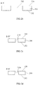
FIGS. 2a to 2e are structural diagrams of a package substrate according to an embodiment of the disclosure; -
FIG. 3 is a schematic illustration of a structure of a package substrate in accordance with an embodiment of the present disclosure; -
FIG. 4a is a schematic illustration of a structure of a package substrate in accordance with an embodiment of the present disclosure; -
FIG. 4b is a schematic illustration of a structure of a package substrate according to an embodiment of the disclosure; -
FIG. 5 is a structural diagram of a package substrate in accordance with an embodiment of the present disclosure; -
FIG. 6 is a structural diagram of a package substrate in accordance with an embodiment of the present disclosure; -
FIG. 7 is a structural diagram of a package substrate in accordance with an embodiment of the present disclosure; -
Figs. 8a-8c are structural schematic views of a package substrate according to an embodiment of the disclosure; -
FIG. 9 is a schematic illustration of a packaging structure according to an embodiment of the present disclosure. - As described in the background, air holes in prior art are formed on the substrate to facilitate gas venting in the short side direction of the chip during injection molding and to improve the filling effect of the mold compound in the short side direction. However, in the direction of the long side of the chip, there is still a problem of filling such as bubbles.
- The inventors have found that in the direction of the long side of the chip, a more pronounced peristaltic flow (Re « 1 in fluid mechanics, or low Reynolds number flow) is generated as the mold compound needs to flow through more solder bump areas, resulting in turbulent influx of the mold compound containing more air bubbles and thus poor venting effect through a single circular hole; This problem can be ameliorated by arranging more air holes in the direction of the long side of the chip, however, more air holes will occupy the area of the soldering region between the chip and the substrate, so that the soldering region is dispersed and design area is wasted.
- The inventors have further discovered that air holes in prior art are provided in a circular shape, it will be difficult for the mold compound to pass through when solid or semi-solid impurities are contained in the mold compound, or the mold compound may cause the air holes to become blocked, resulting in more serious filling abnormalities. Referring now to
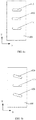
FIG. 1 , where thesubstrate 100 is centrally provided with agas hole 101,impurities 102 in the mold compound that are larger or comparable to the diameter of thegas hole 101 are difficult to escape or detach from thegas hole 101 regardless of how theimpurities 102 change position, are very prone to getting stuck within thegas hole 101, resulting in gas that cannot be removed. While hole apertures can be expanded directly to ameliorate problems such as air bubbles and clogging, the solder bumps of the chip and the soldering region of the substrate are also excessively occupied, and the mold compound can droop directly from the hole with large diameter, resulting in unfilled mold compound filling in the area around the hole. - Based on the above studies, the inventors propose a new package substrate and a method for forming the same, and a package structure based on the package substrate and a method for forming the same, to solve the above-described problems.
- Specific embodiments of package substrates and methods of forming the same, package structures and methods of forming the same provided herein are described in detail below with reference to the accompanying drawings.
- Referring now to
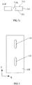
FIGS. 2a-2c , schematic illustrations of a package substrate in accordance with an embodiment of the present disclosure are shown.FIG. 2a is a schematic top view of thesubstrate 200,FIG. 2b is a schematic cross-sectional view along secant AA 'inFIG. 2a andFIG. 2c is a schematic cross-sectional view along secant BB' inFIG. 2a . - The package substrate includes a
substrate 200, and avent hole 210 through thesubstrate 200. - The
substrate 200 has opposingfirst surface 201 andsecond surface 202. Thesubstrate 200 may be a circuit board having electrical connection structure like interconnect circuitry, pads, etc. formed on the surface of thesubstrate 200 and/or within thesubstrate 200, for making electrical connections to the chip, inputting electrical signals to the chip, or outputting electrical signals generated by the chip. The shape of thesubstrate 200 generally corresponds to the shape of the chip to be packaged, being square or rectangular. In this embodiment, thesubstrate 200 has a rectangular shape with a length along the Y direction and a width along the X direction. - The
vent hole 210 is a long-strip hole extending through thefirst surface 201 and thesecond surface 202 of thesubstrate 200. The region of thefirst surface 201 of thesubstrate 200 outside of thevent hole 210 is a soldering region, with a metal connection layer formed for soldering with the chip to be packaged. In other embodiments, thevent hole 210 includes at least one long-strip hole, and other hole structures in communication with the long-strip hole. In this embodiment, thevent hole 210 is in the shape of long straight lines, in other embodiments, thevent hole 210 may also be broken line or curved lines, and in particular the vent hole may be shaped according to the distribution of the solder bumps. While increasing the venting effect, by avoiding overly dispersed soldered regions on thesubstrate 200, the waste of area can be reduced. - When the
vent hole 210 has a long-strip shape, the aperture area is larger and the venting effect is better; and, if solid or semi-solid impurities are contained within the mold compound, the impurities are less likely to get stuck within the vent hole with the following of the mold compound, thereby reducing instances of thevent hole 210 becoming blocked. Also, even if the impurities get stuck inside thevent hole 210, gas can be vented from both sides of the impurities because thevent hole 210 has the long-strip shape, thereby preventing the possibility of the vent holes being completely blocked. - In this embodiment, the length direction of the
vent hole 210 coincides with the length direction of thesubstrate 200. Since the mold compound flows a longer distance in the Y-axis direction of thesubstrate 200 during the injection molding process, more solder bumps are passed through, thevent hole 210 has a longer length in the Y-direction, which can improve the venting effect in the Y-direction. And thevent hole 210 is disposed along the axis of symmetry of thesubstrate 200, and is symmetric about the axis of symmetry. Since the mold compound typically flows from the edge to the center of thesubstrate 200 during the injection molding process, thevent hole 210 being provided at the position of axis of symmetry may improve the uniformity of the venting. - The width to length ratio of the
vent hole 210 ranges from 1: 1.3 to 1:15 for a better venting effect. Preferably, the width to length ratio of thevent hole 210 ranges from 1: 2 to 1: 7 to provide a better venting effect and avoid occupying a large substrate area. - In other embodiments, two or more vent holes may also be formed within the
substrate 200. - Referring now to
FIG. 3 , a schematic top view of a package substrate in accordance with another embodiment of the present disclosure is shown. In this embodiment, twovent holes 310 are formed in thesubstrate 300, each of which is a long-strip hole, the length direction of the vent holes 310 coincides with the length direction of thesubstrate 300 and the vent holes are distributed along the axis of symmetry. - Referring now to
FIG. 4a , there is a schematic top view of a package substrate in accordance with another embodiment of the present disclosure. In this embodiment, threevent holes 410 are formed in thesubstrate 400, the length directions of the vent holes 410 may coincide with the width direction of thesubstrate 300, and the vent holes are uniformly distributed along the width direction of thesubstrate 400. - Referring now to
Fig. 4b , there is a schematic top view of a package substrate according to another embodiment wherein twovent holes 420 are arranged obliquely. - In other embodiments, the number and distribution of the vent holes 410, 420 on the
substrate 200 can be set properly based on the distribution of the soldering region on thesubstrate 200 and simulated effects of the flow rate of the mold compound fluid, etc. The length to width ratio of the long-strip holes of the vent holes 410, 420 is 1: 1.3 to 1: 15, which has a better effect of venting and avoiding clogging by impurities. - In other embodiments, the substrate may also have at least one circular hole formed through the first surface and the second surface of the substrate. The circular holes may be distributed across a central axis of the substrate, preferably, distributed on a central axis along the length direction of the substrate.
- Referring now to
FIG. 5 , a schematic top view of a package substrate in accordance with another embodiment of the present disclosure is shown. - In this embodiment, the vent holes 510 in the
substrate 500 include two cross-connected long-strip holes 510 and 520, in a crisscross shape. In this embodiment, the sizes of thehole 501 and thehole 502 are the same, and the length directions of the holes coincide with the length and width directions of thesubstrate 500, respectively. And thehole 510 is located at a central position of thesubstrate 500. In another embodiment, the sizes of thehole 501 and thehole 502 may also be different, preferably the length of thehole 501 extending along the long side of thesubstrate 500 is greater than the length of thehole 502 extending along the short side of thesubstrate 500. - In other embodiments, the vent hole may further comprise three or more cross-connected long-strip holes, the cross angles may be perpendicular or oblique to each other, and the cross locations may be located in the middle or in the ends, without being limited here.
- With continued reference to
FIG. 2a , thevent hole 210 has a smooth inner wall edge. In particular, the cross-sectional edge of thevent hole 210 parallel to the surface of thesubstrate 200 has smooth lines, and has an arc connect at the position of the corner of the length connecting the width to avoid sharp corner inside thevent hole 210 causing turbulent flow when the gas or fluid passing through, thereby affecting the filling effect of the mold compound. Thevent hole 210 may be formed by drilling, laser etching, etching, or the like. Further, the inner wall surface of thevent hole 210 may also be passivated so that the inner wall surface of thevent hole 210 has a passivation surface to ensure that thevent hole 210 has a smooth inner wall edge. The passivation surface may be a passivation layer surface covering the sidewall of thevent hole 210. - In this embodiment, the sidewall of the
vent hole 210 is perpendicular to the surface of thesubstrate 200. In other embodiments, thevent hole 210 may also have a sloped side wall (please refer to venthole 210a inFig. 2d ), or a side wall having a larger middle dimension and two smaller ends (please refer to venthole 210b inFig. 2e ), without being limited here. - Referring now to
FIG. 6 , a schematic top view of a package substrate in accordance with an embodiment of the present disclosure is shown. - The
vent hole 610 within thepackage substrate 600 is formed by connecting a plurality of continuous circular holes 601. The size of each of thecircular holes 601 is the same, and the size and shape of thevent hole 610 can be adjusted by controlling the number and arrangement of thecircular holes 601, and the adjustment is easy to be realized. - In this embodiment, the
vent hole 610 is connected by circular holes, with a protruding sharp corner where the edges of adjacent circular holes meet, so that the smoothness of thevent hole 610 is to be improved. - Referring now to
FIG. 7 , there is a schematic illustration of a package substrate in accordance with another embodiment of the present disclosure. - On the basis of the package substrate shown in
Fig. 6 , apassivation layer 710 is formed on the inner wall surface of thevent hole 610. Bypassivation layer 710, the angle of the protruding sharp corner of the inner wall of thevent hole 610 becomes flat, and the surface of thevent hole 610 becomes arc-shaped, reducing the risk of turbulent flow when the gas or fluid passing through thevent hole 610. - The
passivation layer 710 may be formed by a metallization process. In some embodiments, thepassivation layer 710 may be a metal layer formed by a sputtering process, such as a Cu layer, a W layer, or the like. - In other embodiments, the
passivation layer 710 may also be formed on the inner wall surface of thevent hole 610 by chemical deposition. Thepassivation layer 710 may also be formed from other materials that tend to cover the inner wall of the vent hole. - In other embodiments, the inner wall of the
vent hole 610 may also be smoothed to remove sharp corners by grinding the inner wall of thevent hole 610, such that there is no sharp protrusion one the inner wall of thevent hole 610. - The package substrate in the above detailed description, having long-strip vent holes, can increase the venting effect and reduce the risk of the vent holes being blocked during injection molding. Also, while increasing the venting effect, the number of vent holes is reduced so that the soldering region between the substrate and the chip is more concentrated, avoiding wasting design area.
- Embodiments of the present disclosure also provide a structural schematic of the above-described formation process of the package substrate.
- Take the package substrate shown in
FIG. 2a as an example. - First, a
substrate 200 is provided having opposingfirst surface 201 andsecond surface 202. Thesubstrate 200 may be a circuit board having electrical connection structure like interconnect circuitry, pads, etc. formed on the surface of thesubstrate 200 and/or within thesubstrate 200, so that thesubstrate 200 may be electrically connected to the chip, inputting electrical signals to the chip or outputting electrical signals generated by the chip. The shape of thesubstrate 200 generally corresponds to the shape of the chip to be packaged, being square or rectangular. - A
vent hole 210 is then formed within thesubstrate 200, extending through thefirst surface 201 and thesecond surface 202 of thesubstrate 200, thevent hole 210 is a long-strip hole. - The region of the
first surface 201 of thesubstrate 200 outside of thevent hole 210 is a soldering region, with a metal connection layer formed for soldering with the chip to be packaged. In other embodiments, thevent hole 210 includes at least one long-strip hole, and other hole structures in communication with the long-strip hole. In this embodiment, thevent hole 210 is in the shape of long straight lines, and in other embodiments, thevent hole 210 may also be broken lines or curved lines. While increasing the venting effect, by avoiding overly dispersed the soldering regions on thesubstrate 200, the waste of area can be reduced. - In this embodiment, the length direction of the
vent hole 210 coincides with the length direction of thesubstrate 200. In other embodiments, the length direction of thevent hole 210 may also coincide with the width direction of thesubstrate 200, or may be arranged obliquely.. - In other embodiments, two or more vent holes may also be formed within the
substrate 200. The vent hole also includes two or more cross-connected long-strip holes. - The length to width ratio of the long-strip hole is 1: 1.3 to 1: 15, preferably 1: 2 to 1: 7.
- In other embodiments, the substrate may also have at least one circular hole formed through the first surface and the second surface of the substrate. The circular holes may be distributed on a central axis of the substrate, preferably, distributed on a central axis along the length direction of the substrate.
- The numbers, locations, shapes, and sizes of the vent holes formed can be reasonably set as desired by those skilled in the art, without being limited here.
- Referring now to
FIGS. 8a to 8c , schematic illustrations of the vent hole formation process are shown in accordance with an implementation of the disclosure. - Referring now to
FIG. 8a , acircular hole 801 is formed on thesubstrate 800.FIG. 8a includes a schematic top view of thecircular hole 801 formed by drilling, and a schematic cross-sectional view along secant lines CC in the schematic top view; - Referring to
FIG. 8b , acircular hole 802 of the same size is formed by drilling on the edge of thecircular hole 801, with an overlap between thecircular hole 802 and thecircular hole 801 such that thecircular hole 802 communicates with thecircular hole 801. - Referring to
FIG. 8c ,circular hole 803 andcircular hole 804 are continuously formed along the same straight line, circular holes 801-804 communicate with each other to form a long-strip vent hole 810. - Subsequent passivation treatment may be performed on the inner wall surface of the
vent hole 810, such as forming a passivation layer or performing a grinding layer process, such that the inner wall surface of thevent hole 810 is smoother and free of sharp protrusions. - The passivation process may be a metallization process. In one embodiment, the metallization process includes: forming a metal layer on the inner wall surface of the formed
vent hole 810 and the surface of thesubstrate 800 by, for example, Sputtering process, Plating process, or Metal Vapor Deposition (MOCVD) process; the metal layer on the surface of thesubstrate 800 is then removed by methods such as grinding or etching, leaving only the metal layer covering the inner wall of thevent hole 810 as a passivation layer. If, after grinding or etching, the thickness of the metal layer covered within thevent hole 810 is too large, it can be re-drilled by using a drill with a smaller aperture, only leaving a thinner metal layer as the passivation layer. Wherein, the material for the metal layer may be metal materials commonly used in semiconductor processes, such as W or Cu. - An implementation of the disclosure also provides a package structure employing the package substrate described above.
- Referring now to
FIG. 9 , a schematic illustration of a packaging structure in accordance with a specific implementation of the present disclosure is shown. - In this particular implementation, the package substrate described in
FIG. 2b is taken as an example. - The packaging structure includes a package substrate including a
substrate 200 and avent hole 210 extending through thesubstrate 200; achip 900 flip-chip fixed on thefirst surface 201 of thesubstrate 200 bysolder bumps 901, forming electrical connections between the solder bumps 901 and thesubstrate 200, thevent hole 210 being located within a projection of thechip 900 on thesubstrate 200; amold compound 910, enclosing thechip 900 and filling the gap between thechip 900 and thefirst surface 201 of thesubstrate 200 and thevent hole 210. - The
vent hole 210 in the package is long-strip hole extending through thefirst surface 201 and thesecond surface 202 of thesubstrate 200. - The packaging structure also includes
solder balls 920 formed on thesecond surface 202 of thesubstrate 200. - In the above-described package structure, since the long-strip vent holes are formed in the package substrate, the filling effect of the
mold compound 910 can be effectively improved in various directions, such that themold compound 910 sufficiently fills the gap between thechip 900 and thesubstrate 200, reducing problems of poor filling such as air holes etc., and improving the reliability of the package structure. - The vent holes within the package substrate of the package structure can also adopt other configurations, with specific reference to the descriptions in the preceding detailed description, which are not repeated here.
- Embodiments of the present disclosure also provide a method of forming the package structure described above.
- The method of forming the package structure comprises the steps of:
- Step 1: providing a package substrate having opposing first surface and second surface; at least one vent hole extending through the first surface and the second surface of the substrate, the vent hole comprising at least a long-strip hole.
- Step 2: flip-chip fixing a chip on a first surface of the substrate with solder bumps by a flip chip process, forming electrical connections between the solder bumps and the substrate, the vent hole within the substrate being located within a projection of the chip on the substrate.
- Step 3: performing a injection molding process of the chip flip-chip onto the substrate, enclosing the chip and filling the gap between the chip and the first surface of the substrate and the vent hole with a mold compound.
- A substrate with a flip chip on the surface can be placed within a cavity of the injection mold, and a second surface of the substrate is located on the bottom surface of the cavity; then, a liquid mold compound is injected into the cavity and curing process is performed, the mold compound fills the cavity, encloses the chip, and fills the chip-to-substrate surface gap.
- During injection of the mold compound, gas within the cavity is vented through at least some of the vent holes. The cavity bottom can have grooves in communication with vent holes in the substrate, the grooves are communicated with the outside of the packaging mold to vent gas out of the cavity.
- Since the vent holes comprise long-strip holes, the vent holes are not easy to be blocked, and have a large aperture, the venting efficiency is improved. Therefore, it may continue to serve as a gas venting channel before the mold compound completely fills the cavity, enhancing the filling effect of the mold compound.
- Step 4: forming solder balls on the second surface of the substrate.
- After the injection molding process is completed, solder balls, which may be soldering lead tin balls or lead-free tin balls, etc., are formed on the second surface of the substrate. The package structure may be subsequently affixed to other electronic components, such as other circuit boards through the solder balls via a reflow soldering process.
- What has been described above is merely the preferred embodiments of the present disclosure, and it should be noted that numerous modifications and modifications can be made to those skilled in the art without departing from the principles of the disclosure, which are also to be regarded as protective in the scope of the disclosure.
Claims (20)
- A package substrate comprising:a substrate having opposing first surface and second surface;at least one vent hole extending through the first surface and the second surface of the substrate, the vent hole comprising at least a long-strip hole.
- The package substrate of claim 1, wherein the vent hole comprises at least two cross-connected long-strip holes.
- The package substrate of claim 1, comprising more than two vent holes uniformly distributed in a length direction of the package substrate.
- The package substrate of claim 1, wherein the vent hole is symmetric about an axis of symmetry of the package substrate.
- The package substrate of claim 1, wherein a cross-sectional edge of the vent hole parallel to the substrate surface has a smooth line.
- The package substrate of claim 1, wherein the long-strip hole is formed by connecting a plurality of continuous circular holes.
- The package substrate of claim 1, wherein the inner wall of the vent hole has a passivation surface.
- The package substrate of claim 1, wherein the long-strip hole has a width to length ratio ranging from 1:1.3 to 1:15.
- The package substrate of claim 1, further comprising at least one circular hole distributed across a central axis of the substrate.
- A method of forming a package substrate, comprising:providing a substrate having a first surface and a second surface;forming at least one vent hole, the vent hole extending through the first surface and the second surface of the substrate, the vent hole including at least a long-strip hole.
- The method of forming a package substrate of claim 10, wherein the vent hole comprises at least two cross-connected long-strip holes.
- The method of forming a package substrate of claim 10, comprising more than two vent holes uniformly distributed in a length direction of the package substrate.
- The method of forming a package substrate of claim 10, wherein the vent hole is symmetric about an axis of symmetry of the package substrate.
- The method of forming a package substrate of claim 10, wherein a cross-sectional edge of the vent hole parallel to the substrate surface has a smooth line.
- The method of forming a package substrate of claim 10, wherein the long-strip hole is formed by forming a plurality of continuous circular holes through the substrate, and the plurality of continuous circular holes are interconnected to form the long-strip hole.
- The method of forming a package substrate of claim 10, further comprising: performing a passivation process on an inner wall surface of the vent hole.
- The method of forming a package substrate of claim 10, wherein the long-strip hole has a width to length ratio ranging from 1: 1.3 to 1: 15.
- The method of forming a package substrate of claim 10, further comprising forming at least one circular hole distributed across a central axis of the substrate.
- A package structure comprising:a package substrate as claimed in any one of claims 1;a chip, flip-chip fixed on a first surface of the substrate with solder bumps, forming electrical connections between the chip and the substrate with the solder bumps the vent hole being located within a projection of the chip on the substrate;a mold compound enclosing the chip and filling a gap between the chip and the first surface of the substrate and the vent hole.
- A method of forming a package structure, comprising:providing a package substrate as claimed in any one of claims 1;flip-chip fixing a chip on a first surface of the substrate with solder bumps by a flip-chip process,forming electrical connections between the chip and the substrate with the solder bumps, the vent hole within the substrate being located within a projection of the chip on the substrate;performing an injection molding process on the chip flipped onto the substrate, enclosing the chip and filling a gap between the chip and the first surface of the substrate and the vent holes with a mold compound.
Applications Claiming Priority (2)
| Application Number | Priority Date | Filing Date | Title |
|---|---|---|---|
| CN202010102444.1A CN113284855B (en) | 2020-02-19 | 2020-02-19 | Package substrate and forming method thereof, package structure and forming method thereof |
| PCT/CN2020/128342 WO2021164337A1 (en) | 2020-02-19 | 2020-11-12 | Package substrate and forming method therefor, and package structure and forming method therefor |
Publications (3)
| Publication Number | Publication Date |
|---|---|
| EP3933910A1 true EP3933910A1 (en) | 2022-01-05 |
| EP3933910A4 EP3933910A4 (en) | 2022-07-06 |
| EP3933910B1 EP3933910B1 (en) | 2023-06-21 |
Family
ID=77275072
Family Applications (1)
| Application Number | Title | Priority Date | Filing Date |
|---|---|---|---|
| EP20919808.4A Active EP3933910B1 (en) | 2020-02-19 | 2020-11-12 | Package substrate and forming method therefor, and package structure and forming method therefor |
Country Status (4)
| Country | Link |
|---|---|
| US (1) | US12027379B2 (en) |
| EP (1) | EP3933910B1 (en) |
| CN (1) | CN113284855B (en) |
| WO (1) | WO2021164337A1 (en) |
Families Citing this family (2)
| Publication number | Priority date | Publication date | Assignee | Title |
|---|---|---|---|---|
| CN115346933A (en) * | 2022-08-10 | 2022-11-15 | 华天科技(南京)有限公司 | Plastic package structure for improving product cavity in plastic package process and packaging method thereof |
| CN119275182A (en) * | 2023-06-28 | 2025-01-07 | 长鑫存储技术有限公司 | Semiconductor structure and method for forming the same |
Family Cites Families (21)
| Publication number | Priority date | Publication date | Assignee | Title |
|---|---|---|---|---|
| JPH03157944A (en) | 1989-11-15 | 1991-07-05 | Sony Corp | Semiconductor package |
| US5581038A (en) * | 1994-04-04 | 1996-12-03 | Sentir, Inc. | Pressure measurement apparatus having a reverse mounted transducer and overpressure guard |
| US6239385B1 (en) * | 1998-02-27 | 2001-05-29 | Agilent Technologies, Inc. | Surface mountable coaxial solder interconnect and method |
| US6383846B1 (en) | 2000-03-20 | 2002-05-07 | Chi-Chih Shen | Method and apparatus for molding a flip chip semiconductor device |
| JP4454792B2 (en) * | 2000-05-18 | 2010-04-21 | 富士通マイクロエレクトロニクス株式会社 | Semiconductor device |
| US6617682B1 (en) * | 2000-09-28 | 2003-09-09 | Intel Corporation | Structure for reducing die corner and edge stresses in microelectronic packages |
| US6772512B2 (en) | 2001-01-13 | 2004-08-10 | Siliconware Precision Industries Co., Ltd. | Method of fabricating a flip-chip ball-grid-array package without causing mold flash |
| US6451625B1 (en) * | 2001-01-13 | 2002-09-17 | Siliconware Precision Industries, Co., Ltd. | Method of fabricating a flip-chip ball-grid-array package with molded underfill |
| JP2002261190A (en) * | 2001-02-28 | 2002-09-13 | Sony Corp | Semiconductor device, method of manufacturing the same, and electronic equipment |
| JP4581301B2 (en) * | 2001-06-29 | 2010-11-17 | ソニー株式会社 | Semiconductor package |
| TW498515B (en) * | 2001-08-01 | 2002-08-11 | Siliconware Precision Industries Co Ltd | Flip chip type semiconductor package piece with flash prevention structure and its manufacture method |
| KR20110092045A (en) * | 2010-02-08 | 2011-08-17 | 삼성전자주식회사 | Molded underfill flip chip package suppresses warpage and voids |
| KR101902996B1 (en) | 2012-07-09 | 2018-10-01 | 삼성전자주식회사 | Semiconductor package and method of forming the same |
| GB2504343A (en) | 2012-07-27 | 2014-01-29 | Ibm | Manufacturing an semiconductor chip underfill using air vent |
| DE112013004122T5 (en) * | 2012-08-23 | 2015-05-07 | Ps4 Luxco S.A.R.L. | Component and method for its production |
| KR101965127B1 (en) * | 2012-10-29 | 2019-04-04 | 삼성전자 주식회사 | Semiconductor package and method for fabricating the same |
| CN203590586U (en) | 2013-08-15 | 2014-05-07 | 青岛海信电器股份有限公司 | Circuit board |
| CN104669221A (en) * | 2015-03-17 | 2015-06-03 | 合肥京东方光电科技有限公司 | Insulation machine, equipment and method for eliminating static electricity |
| CN105914155A (en) | 2016-04-29 | 2016-08-31 | 南通富士通微电子股份有限公司 | Flip chip and package method thereof |
| CN209419980U (en) | 2018-08-24 | 2019-09-20 | 珠海格力电器股份有限公司 | Printed wiring board and control device |
| CN211404481U (en) * | 2020-02-19 | 2020-09-01 | 长鑫存储技术有限公司 | Package substrate and package structure |
-
2020
- 2020-02-19 CN CN202010102444.1A patent/CN113284855B/en active Active
- 2020-11-12 WO PCT/CN2020/128342 patent/WO2021164337A1/en not_active Ceased
- 2020-11-12 EP EP20919808.4A patent/EP3933910B1/en active Active
- 2020-11-12 US US17/433,789 patent/US12027379B2/en active Active
Also Published As
| Publication number | Publication date |
|---|---|
| EP3933910B1 (en) | 2023-06-21 |
| US12027379B2 (en) | 2024-07-02 |
| US20220351984A1 (en) | 2022-11-03 |
| EP3933910A4 (en) | 2022-07-06 |
| CN113284855A (en) | 2021-08-20 |
| CN113284855B (en) | 2025-01-10 |
| WO2021164337A1 (en) | 2021-08-26 |
Similar Documents
| Publication | Publication Date | Title |
|---|---|---|
| CN106471612B (en) | Semiconductor devices and its manufacturing method | |
| CN102194768B (en) | Substrate, package substrates, semiconductor package part and manufacture method thereof | |
| CN102376681A (en) | Package substrate | |
| CN106463426B (en) | Semiconductor device and method for manufacturing the same | |
| TWI550782B (en) | Integrated circuit package system with path circuit leads and manufacturing method thereof | |
| CN106981473A (en) | Substrate structure and its manufacturing method | |
| EP3933910B1 (en) | Package substrate and forming method therefor, and package structure and forming method therefor | |
| CN106463472A (en) | Semiconductor device and method of manufacturing same | |
| US20250054828A1 (en) | Electronic package and manufacturing method thereof | |
| CN103137581B (en) | Semiconductor device with conductive bump, package structure and manufacturing method | |
| CN211404481U (en) | Package substrate and package structure | |
| JP5338572B2 (en) | Manufacturing method of semiconductor device | |
| JP5667381B2 (en) | Semiconductor device and manufacturing method thereof | |
| US8466057B2 (en) | Integrated circuit packaging system with filled vias and method of manufacture thereof | |
| CN203118928U (en) | Packaging structure | |
| KR20240001780A (en) | Semiconductor package | |
| CN212342619U (en) | Three-dimensional package structure that piles up of wafer level chip fan-out | |
| US20250038097A1 (en) | Electronic package and manufacturing method thereof, and substrate structure | |
| TWI480988B (en) | Package substrate plate structure, package substrate, semiconductor package and manufacturing method thereof | |
| CN212461680U (en) | Three-dimensional package structure that piles up of wafer level chip fan-out | |
| US20190385921A1 (en) | Packaging structure | |
| US20250062268A1 (en) | Semiconductor packages having trench structures | |
| US10770425B2 (en) | Flip-chip method | |
| CN221977915U (en) | Semiconductor packaging structure | |
| CN223260601U (en) | Package structure |
Legal Events
| Date | Code | Title | Description |
|---|---|---|---|
| STAA | Information on the status of an ep patent application or granted ep patent |
Free format text: STATUS: THE INTERNATIONAL PUBLICATION HAS BEEN MADE |
|
| PUAI | Public reference made under article 153(3) epc to a published international application that has entered the european phase |
Free format text: ORIGINAL CODE: 0009012 |
|
| STAA | Information on the status of an ep patent application or granted ep patent |
Free format text: STATUS: REQUEST FOR EXAMINATION WAS MADE |
|
| 17P | Request for examination filed |
Effective date: 20210929 |
|
| AK | Designated contracting states |
Kind code of ref document: A1 Designated state(s): AL AT BE BG CH CY CZ DE DK EE ES FI FR GB GR HR HU IE IS IT LI LT LU LV MC MK MT NL NO PL PT RO RS SE SI SK SM TR |
|
| A4 | Supplementary search report drawn up and despatched |
Effective date: 20220608 |
|
| RIC1 | Information provided on ipc code assigned before grant |
Ipc: H01L 21/56 20060101ALI20220601BHEP Ipc: H01L 23/31 20060101ALI20220601BHEP Ipc: H01L 23/13 20060101AFI20220601BHEP |
|
| GRAP | Despatch of communication of intention to grant a patent |
Free format text: ORIGINAL CODE: EPIDOSNIGR1 |
|
| STAA | Information on the status of an ep patent application or granted ep patent |
Free format text: STATUS: GRANT OF PATENT IS INTENDED |
|
| DAV | Request for validation of the european patent (deleted) | ||
| DAX | Request for extension of the european patent (deleted) | ||
| INTG | Intention to grant announced |
Effective date: 20230316 |
|
| GRAS | Grant fee paid |
Free format text: ORIGINAL CODE: EPIDOSNIGR3 |
|
| GRAA | (expected) grant |
Free format text: ORIGINAL CODE: 0009210 |
|
| STAA | Information on the status of an ep patent application or granted ep patent |
Free format text: STATUS: THE PATENT HAS BEEN GRANTED |
|
| AK | Designated contracting states |
Kind code of ref document: B1 Designated state(s): AL AT BE BG CH CY CZ DE DK EE ES FI FR GB GR HR HU IE IS IT LI LT LU LV MC MK MT NL NO PL PT RO RS SE SI SK SM TR |
|
| REG | Reference to a national code |
Ref country code: CH Ref legal event code: EP |
|
| P01 | Opt-out of the competence of the unified patent court (upc) registered |
Effective date: 20230531 |
|
| REG | Reference to a national code |
Ref country code: DE Ref legal event code: R096 Ref document number: 602020012874 Country of ref document: DE |
|
| REG | Reference to a national code |
Ref country code: AT Ref legal event code: REF Ref document number: 1581534 Country of ref document: AT Kind code of ref document: T Effective date: 20230715 |
|
| REG | Reference to a national code |
Ref country code: IE Ref legal event code: FG4D |
|
| REG | Reference to a national code |
Ref country code: NL Ref legal event code: FP |
|
| REG | Reference to a national code |
Ref country code: LT Ref legal event code: MG9D |
|
| PG25 | Lapsed in a contracting state [announced via postgrant information from national office to epo] |
Ref country code: SE Free format text: LAPSE BECAUSE OF FAILURE TO SUBMIT A TRANSLATION OF THE DESCRIPTION OR TO PAY THE FEE WITHIN THE PRESCRIBED TIME-LIMIT Effective date: 20230621 Ref country code: NO Free format text: LAPSE BECAUSE OF FAILURE TO SUBMIT A TRANSLATION OF THE DESCRIPTION OR TO PAY THE FEE WITHIN THE PRESCRIBED TIME-LIMIT Effective date: 20230921 |
|
| REG | Reference to a national code |
Ref country code: AT Ref legal event code: MK05 Ref document number: 1581534 Country of ref document: AT Kind code of ref document: T Effective date: 20230621 |
|
| PG25 | Lapsed in a contracting state [announced via postgrant information from national office to epo] |
Ref country code: RS Free format text: LAPSE BECAUSE OF FAILURE TO SUBMIT A TRANSLATION OF THE DESCRIPTION OR TO PAY THE FEE WITHIN THE PRESCRIBED TIME-LIMIT Effective date: 20230621 Ref country code: LV Free format text: LAPSE BECAUSE OF FAILURE TO SUBMIT A TRANSLATION OF THE DESCRIPTION OR TO PAY THE FEE WITHIN THE PRESCRIBED TIME-LIMIT Effective date: 20230621 Ref country code: LT Free format text: LAPSE BECAUSE OF FAILURE TO SUBMIT A TRANSLATION OF THE DESCRIPTION OR TO PAY THE FEE WITHIN THE PRESCRIBED TIME-LIMIT Effective date: 20230621 Ref country code: HR Free format text: LAPSE BECAUSE OF FAILURE TO SUBMIT A TRANSLATION OF THE DESCRIPTION OR TO PAY THE FEE WITHIN THE PRESCRIBED TIME-LIMIT Effective date: 20230621 Ref country code: GR Free format text: LAPSE BECAUSE OF FAILURE TO SUBMIT A TRANSLATION OF THE DESCRIPTION OR TO PAY THE FEE WITHIN THE PRESCRIBED TIME-LIMIT Effective date: 20230922 |
|
| PG25 | Lapsed in a contracting state [announced via postgrant information from national office to epo] |
Ref country code: FI Free format text: LAPSE BECAUSE OF FAILURE TO SUBMIT A TRANSLATION OF THE DESCRIPTION OR TO PAY THE FEE WITHIN THE PRESCRIBED TIME-LIMIT Effective date: 20230621 |
|
| PG25 | Lapsed in a contracting state [announced via postgrant information from national office to epo] |
Ref country code: SK Free format text: LAPSE BECAUSE OF FAILURE TO SUBMIT A TRANSLATION OF THE DESCRIPTION OR TO PAY THE FEE WITHIN THE PRESCRIBED TIME-LIMIT Effective date: 20230621 |
|
| PG25 | Lapsed in a contracting state [announced via postgrant information from national office to epo] |
Ref country code: ES Free format text: LAPSE BECAUSE OF FAILURE TO SUBMIT A TRANSLATION OF THE DESCRIPTION OR TO PAY THE FEE WITHIN THE PRESCRIBED TIME-LIMIT Effective date: 20230621 |
|
| PG25 | Lapsed in a contracting state [announced via postgrant information from national office to epo] |
Ref country code: IS Free format text: LAPSE BECAUSE OF FAILURE TO SUBMIT A TRANSLATION OF THE DESCRIPTION OR TO PAY THE FEE WITHIN THE PRESCRIBED TIME-LIMIT Effective date: 20231021 |
|
| PG25 | Lapsed in a contracting state [announced via postgrant information from national office to epo] |
Ref country code: SM Free format text: LAPSE BECAUSE OF FAILURE TO SUBMIT A TRANSLATION OF THE DESCRIPTION OR TO PAY THE FEE WITHIN THE PRESCRIBED TIME-LIMIT Effective date: 20230621 Ref country code: SK Free format text: LAPSE BECAUSE OF FAILURE TO SUBMIT A TRANSLATION OF THE DESCRIPTION OR TO PAY THE FEE WITHIN THE PRESCRIBED TIME-LIMIT Effective date: 20230621 Ref country code: RO Free format text: LAPSE BECAUSE OF FAILURE TO SUBMIT A TRANSLATION OF THE DESCRIPTION OR TO PAY THE FEE WITHIN THE PRESCRIBED TIME-LIMIT Effective date: 20230621 Ref country code: PT Free format text: LAPSE BECAUSE OF FAILURE TO SUBMIT A TRANSLATION OF THE DESCRIPTION OR TO PAY THE FEE WITHIN THE PRESCRIBED TIME-LIMIT Effective date: 20231023 Ref country code: IS Free format text: LAPSE BECAUSE OF FAILURE TO SUBMIT A TRANSLATION OF THE DESCRIPTION OR TO PAY THE FEE WITHIN THE PRESCRIBED TIME-LIMIT Effective date: 20231021 Ref country code: ES Free format text: LAPSE BECAUSE OF FAILURE TO SUBMIT A TRANSLATION OF THE DESCRIPTION OR TO PAY THE FEE WITHIN THE PRESCRIBED TIME-LIMIT Effective date: 20230621 Ref country code: EE Free format text: LAPSE BECAUSE OF FAILURE TO SUBMIT A TRANSLATION OF THE DESCRIPTION OR TO PAY THE FEE WITHIN THE PRESCRIBED TIME-LIMIT Effective date: 20230621 Ref country code: CZ Free format text: LAPSE BECAUSE OF FAILURE TO SUBMIT A TRANSLATION OF THE DESCRIPTION OR TO PAY THE FEE WITHIN THE PRESCRIBED TIME-LIMIT Effective date: 20230621 Ref country code: AT Free format text: LAPSE BECAUSE OF FAILURE TO SUBMIT A TRANSLATION OF THE DESCRIPTION OR TO PAY THE FEE WITHIN THE PRESCRIBED TIME-LIMIT Effective date: 20230621 |
|
| PG25 | Lapsed in a contracting state [announced via postgrant information from national office to epo] |
Ref country code: PL Free format text: LAPSE BECAUSE OF FAILURE TO SUBMIT A TRANSLATION OF THE DESCRIPTION OR TO PAY THE FEE WITHIN THE PRESCRIBED TIME-LIMIT Effective date: 20230621 |
|
| REG | Reference to a national code |
Ref country code: DE Ref legal event code: R097 Ref document number: 602020012874 Country of ref document: DE |
|
| PLBE | No opposition filed within time limit |
Free format text: ORIGINAL CODE: 0009261 |
|
| STAA | Information on the status of an ep patent application or granted ep patent |
Free format text: STATUS: NO OPPOSITION FILED WITHIN TIME LIMIT |
|
| PG25 | Lapsed in a contracting state [announced via postgrant information from national office to epo] |
Ref country code: DK Free format text: LAPSE BECAUSE OF FAILURE TO SUBMIT A TRANSLATION OF THE DESCRIPTION OR TO PAY THE FEE WITHIN THE PRESCRIBED TIME-LIMIT Effective date: 20230621 |
|
| PG25 | Lapsed in a contracting state [announced via postgrant information from national office to epo] |
Ref country code: SI Free format text: LAPSE BECAUSE OF FAILURE TO SUBMIT A TRANSLATION OF THE DESCRIPTION OR TO PAY THE FEE WITHIN THE PRESCRIBED TIME-LIMIT Effective date: 20230621 |
|
| 26N | No opposition filed |
Effective date: 20240322 |
|
| PG25 | Lapsed in a contracting state [announced via postgrant information from national office to epo] |
Ref country code: SI Free format text: LAPSE BECAUSE OF FAILURE TO SUBMIT A TRANSLATION OF THE DESCRIPTION OR TO PAY THE FEE WITHIN THE PRESCRIBED TIME-LIMIT Effective date: 20230621 |
|
| REG | Reference to a national code |
Ref country code: CH Ref legal event code: PL |
|
| PG25 | Lapsed in a contracting state [announced via postgrant information from national office to epo] |
Ref country code: MC Free format text: LAPSE BECAUSE OF FAILURE TO SUBMIT A TRANSLATION OF THE DESCRIPTION OR TO PAY THE FEE WITHIN THE PRESCRIBED TIME-LIMIT Effective date: 20230621 |
|
| PG25 | Lapsed in a contracting state [announced via postgrant information from national office to epo] |
Ref country code: LU Free format text: LAPSE BECAUSE OF NON-PAYMENT OF DUE FEES Effective date: 20231112 |
|
| PG25 | Lapsed in a contracting state [announced via postgrant information from national office to epo] |
Ref country code: CH Free format text: LAPSE BECAUSE OF NON-PAYMENT OF DUE FEES Effective date: 20231130 |
|
| PG25 | Lapsed in a contracting state [announced via postgrant information from national office to epo] |
Ref country code: MC Free format text: LAPSE BECAUSE OF FAILURE TO SUBMIT A TRANSLATION OF THE DESCRIPTION OR TO PAY THE FEE WITHIN THE PRESCRIBED TIME-LIMIT Effective date: 20230621 Ref country code: LU Free format text: LAPSE BECAUSE OF NON-PAYMENT OF DUE FEES Effective date: 20231112 Ref country code: CH Free format text: LAPSE BECAUSE OF NON-PAYMENT OF DUE FEES Effective date: 20231130 |
|
| REG | Reference to a national code |
Ref country code: BE Ref legal event code: MM Effective date: 20231130 |
|
| REG | Reference to a national code |
Ref country code: IE Ref legal event code: MM4A |
|
| PG25 | Lapsed in a contracting state [announced via postgrant information from national office to epo] |
Ref country code: IE Free format text: LAPSE BECAUSE OF NON-PAYMENT OF DUE FEES Effective date: 20231112 |
|
| PG25 | Lapsed in a contracting state [announced via postgrant information from national office to epo] |
Ref country code: BE Free format text: LAPSE BECAUSE OF NON-PAYMENT OF DUE FEES Effective date: 20231130 |
|
| PG25 | Lapsed in a contracting state [announced via postgrant information from national office to epo] |
Ref country code: IE Free format text: LAPSE BECAUSE OF NON-PAYMENT OF DUE FEES Effective date: 20231112 Ref country code: BE Free format text: LAPSE BECAUSE OF NON-PAYMENT OF DUE FEES Effective date: 20231130 |
|
| PG25 | Lapsed in a contracting state [announced via postgrant information from national office to epo] |
Ref country code: BG Free format text: LAPSE BECAUSE OF FAILURE TO SUBMIT A TRANSLATION OF THE DESCRIPTION OR TO PAY THE FEE WITHIN THE PRESCRIBED TIME-LIMIT Effective date: 20230621 |
|
| PG25 | Lapsed in a contracting state [announced via postgrant information from national office to epo] |
Ref country code: BG Free format text: LAPSE BECAUSE OF FAILURE TO SUBMIT A TRANSLATION OF THE DESCRIPTION OR TO PAY THE FEE WITHIN THE PRESCRIBED TIME-LIMIT Effective date: 20230621 |
|
| PG25 | Lapsed in a contracting state [announced via postgrant information from national office to epo] |
Ref country code: CY Free format text: LAPSE BECAUSE OF FAILURE TO SUBMIT A TRANSLATION OF THE DESCRIPTION OR TO PAY THE FEE WITHIN THE PRESCRIBED TIME-LIMIT; INVALID AB INITIO Effective date: 20201112 |
|
| PG25 | Lapsed in a contracting state [announced via postgrant information from national office to epo] |
Ref country code: HU Free format text: LAPSE BECAUSE OF FAILURE TO SUBMIT A TRANSLATION OF THE DESCRIPTION OR TO PAY THE FEE WITHIN THE PRESCRIBED TIME-LIMIT; INVALID AB INITIO Effective date: 20201112 |
|
| REG | Reference to a national code |
Ref country code: DE Ref legal event code: R079 Ref document number: 602020012874 Country of ref document: DE Free format text: PREVIOUS MAIN CLASS: H01L0023130000 Ipc: H10W0070680000 |
|
| PG25 | Lapsed in a contracting state [announced via postgrant information from national office to epo] |
Ref country code: TR Free format text: LAPSE BECAUSE OF FAILURE TO SUBMIT A TRANSLATION OF THE DESCRIPTION OR TO PAY THE FEE WITHIN THE PRESCRIBED TIME-LIMIT Effective date: 20230621 |
|
| PGFP | Annual fee paid to national office [announced via postgrant information from national office to epo] |
Ref country code: NL Payment date: 20251119 Year of fee payment: 6 |
|
| PGFP | Annual fee paid to national office [announced via postgrant information from national office to epo] |
Ref country code: DE Payment date: 20251119 Year of fee payment: 6 |
|
| PGFP | Annual fee paid to national office [announced via postgrant information from national office to epo] |
Ref country code: GB Payment date: 20251121 Year of fee payment: 6 |
|
| PGFP | Annual fee paid to national office [announced via postgrant information from national office to epo] |
Ref country code: IT Payment date: 20251125 Year of fee payment: 6 |
|
| PGFP | Annual fee paid to national office [announced via postgrant information from national office to epo] |
Ref country code: FR Payment date: 20251126 Year of fee payment: 6 |