EP3929327A1 - Light-absorbing/heat-insulating film, light-absorbing/heat-insulating member, article, and manufacturing methods therefor - Google Patents
Light-absorbing/heat-insulating film, light-absorbing/heat-insulating member, article, and manufacturing methods therefor Download PDFInfo
- Publication number
- EP3929327A1 EP3929327A1 EP20783879.8A EP20783879A EP3929327A1 EP 3929327 A1 EP3929327 A1 EP 3929327A1 EP 20783879 A EP20783879 A EP 20783879A EP 3929327 A1 EP3929327 A1 EP 3929327A1
- Authority
- EP
- European Patent Office
- Prior art keywords
- light
- absorbing heat
- shielding film
- shielding
- article
- Prior art date
- Legal status (The legal status is an assumption and is not a legal conclusion. Google has not performed a legal analysis and makes no representation as to the accuracy of the status listed.)
- Pending
Links
- 238000004519 manufacturing process Methods 0.000 title description 6
- 229910052751 metal Inorganic materials 0.000 claims abstract description 86
- 239000002184 metal Substances 0.000 claims abstract description 83
- 239000010410 layer Substances 0.000 claims description 86
- PNEYBMLMFCGWSK-UHFFFAOYSA-N aluminium oxide Inorganic materials [O-2].[O-2].[O-2].[Al+3].[Al+3] PNEYBMLMFCGWSK-UHFFFAOYSA-N 0.000 claims description 68
- 230000001788 irregular Effects 0.000 claims description 68
- 229910044991 metal oxide Inorganic materials 0.000 claims description 61
- 150000004706 metal oxides Chemical class 0.000 claims description 61
- 239000000758 substrate Substances 0.000 claims description 53
- 238000000034 method Methods 0.000 claims description 48
- 229910052782 aluminium Inorganic materials 0.000 claims description 43
- PXHVJJICTQNCMI-UHFFFAOYSA-N Nickel Chemical compound [Ni] PXHVJJICTQNCMI-UHFFFAOYSA-N 0.000 claims description 35
- XAGFODPZIPBFFR-UHFFFAOYSA-N aluminium Chemical compound [Al] XAGFODPZIPBFFR-UHFFFAOYSA-N 0.000 claims description 31
- 239000013078 crystal Substances 0.000 claims description 18
- 239000000463 material Substances 0.000 claims description 18
- 230000003746 surface roughness Effects 0.000 claims description 18
- 229910052759 nickel Inorganic materials 0.000 claims description 17
- XLYOFNOQVPJJNP-UHFFFAOYSA-N water Substances O XLYOFNOQVPJJNP-UHFFFAOYSA-N 0.000 claims description 15
- 239000012790 adhesive layer Substances 0.000 claims description 13
- 238000007654 immersion Methods 0.000 claims description 10
- HCHKCACWOHOZIP-UHFFFAOYSA-N Zinc Chemical compound [Zn] HCHKCACWOHOZIP-UHFFFAOYSA-N 0.000 claims description 6
- 238000010438 heat treatment Methods 0.000 claims description 6
- 229910052725 zinc Inorganic materials 0.000 claims description 6
- 239000011701 zinc Substances 0.000 claims description 6
- VYZAMTAEIAYCRO-UHFFFAOYSA-N Chromium Chemical compound [Cr] VYZAMTAEIAYCRO-UHFFFAOYSA-N 0.000 claims description 4
- 229910052804 chromium Inorganic materials 0.000 claims description 4
- 239000011651 chromium Substances 0.000 claims description 4
- 239000000243 solution Substances 0.000 description 37
- 108010025899 gelatin film Proteins 0.000 description 28
- -1 polyethylene terephthalate Polymers 0.000 description 28
- 238000005530 etching Methods 0.000 description 26
- HEMHJVSKTPXQMS-UHFFFAOYSA-M Sodium hydroxide Chemical compound [OH-].[Na+] HEMHJVSKTPXQMS-UHFFFAOYSA-M 0.000 description 21
- 238000000576 coating method Methods 0.000 description 19
- 239000011248 coating agent Substances 0.000 description 18
- 238000009713 electroplating Methods 0.000 description 17
- 238000005259 measurement Methods 0.000 description 17
- 238000001228 spectrum Methods 0.000 description 16
- 238000007747 plating Methods 0.000 description 14
- 238000010586 diagram Methods 0.000 description 13
- 239000007864 aqueous solution Substances 0.000 description 12
- 239000002585 base Substances 0.000 description 11
- 150000001875 compounds Chemical class 0.000 description 10
- 238000007772 electroless plating Methods 0.000 description 9
- VEXZGXHMUGYJMC-UHFFFAOYSA-N Hydrochloric acid Chemical compound Cl VEXZGXHMUGYJMC-UHFFFAOYSA-N 0.000 description 8
- VYPSYNLAJGMNEJ-UHFFFAOYSA-N Silicium dioxide Chemical compound O=[Si]=O VYPSYNLAJGMNEJ-UHFFFAOYSA-N 0.000 description 8
- 230000008569 process Effects 0.000 description 8
- 229920005989 resin Polymers 0.000 description 8
- 239000011347 resin Substances 0.000 description 8
- 239000011358 absorbing material Substances 0.000 description 7
- 230000000052 comparative effect Effects 0.000 description 7
- 238000004528 spin coating Methods 0.000 description 7
- LFQSCWFLJHTTHZ-UHFFFAOYSA-N Ethanol Chemical compound CCO LFQSCWFLJHTTHZ-UHFFFAOYSA-N 0.000 description 6
- KFZMGEQAYNKOFK-UHFFFAOYSA-N Isopropanol Chemical compound CC(C)O KFZMGEQAYNKOFK-UHFFFAOYSA-N 0.000 description 6
- 229920000620 organic polymer Polymers 0.000 description 5
- NRNCYVBFPDDJNE-UHFFFAOYSA-N pemoline Chemical compound O1C(N)=NC(=O)C1C1=CC=CC=C1 NRNCYVBFPDDJNE-UHFFFAOYSA-N 0.000 description 5
- 239000000047 product Substances 0.000 description 5
- 239000003381 stabilizer Substances 0.000 description 5
- WOZZOSDBXABUFO-UHFFFAOYSA-N tri(butan-2-yloxy)alumane Chemical compound [Al+3].CCC(C)[O-].CCC(C)[O-].CCC(C)[O-] WOZZOSDBXABUFO-UHFFFAOYSA-N 0.000 description 5
- RTZKZFJDLAIYFH-UHFFFAOYSA-N Diethyl ether Chemical compound CCOCC RTZKZFJDLAIYFH-UHFFFAOYSA-N 0.000 description 4
- OAICVXFJPJFONN-UHFFFAOYSA-N Phosphorus Chemical compound [P] OAICVXFJPJFONN-UHFFFAOYSA-N 0.000 description 4
- QAOWNCQODCNURD-UHFFFAOYSA-N Sulfuric acid Chemical compound OS(O)(=O)=O QAOWNCQODCNURD-UHFFFAOYSA-N 0.000 description 4
- 238000004833 X-ray photoelectron spectroscopy Methods 0.000 description 4
- 230000015572 biosynthetic process Effects 0.000 description 4
- 239000003960 organic solvent Substances 0.000 description 4
- 239000011574 phosphorus Substances 0.000 description 4
- 229910052698 phosphorus Inorganic materials 0.000 description 4
- 150000003839 salts Chemical class 0.000 description 4
- ZWEHNKRNPOVVGH-UHFFFAOYSA-N 2-Butanone Chemical compound CCC(C)=O ZWEHNKRNPOVVGH-UHFFFAOYSA-N 0.000 description 3
- QTBSBXVTEAMEQO-UHFFFAOYSA-N Acetic acid Chemical compound CC(O)=O QTBSBXVTEAMEQO-UHFFFAOYSA-N 0.000 description 3
- CSCPPACGZOOCGX-UHFFFAOYSA-N Acetone Chemical compound CC(C)=O CSCPPACGZOOCGX-UHFFFAOYSA-N 0.000 description 3
- XEKOWRVHYACXOJ-UHFFFAOYSA-N Ethyl acetate Chemical compound CCOC(C)=O XEKOWRVHYACXOJ-UHFFFAOYSA-N 0.000 description 3
- LYCAIKOWRPUZTN-UHFFFAOYSA-N Ethylene glycol Chemical compound OCCO LYCAIKOWRPUZTN-UHFFFAOYSA-N 0.000 description 3
- OKKJLVBELUTLKV-UHFFFAOYSA-N Methanol Chemical compound OC OKKJLVBELUTLKV-UHFFFAOYSA-N 0.000 description 3
- VEQPNABPJHWNSG-UHFFFAOYSA-N Nickel(2+) Chemical compound [Ni+2] VEQPNABPJHWNSG-UHFFFAOYSA-N 0.000 description 3
- 239000004721 Polyphenylene oxide Substances 0.000 description 3
- KWYUFKZDYYNOTN-UHFFFAOYSA-M Potassium hydroxide Chemical compound [OH-].[K+] KWYUFKZDYYNOTN-UHFFFAOYSA-M 0.000 description 3
- XUIMIQQOPSSXEZ-UHFFFAOYSA-N Silicon Chemical compound [Si] XUIMIQQOPSSXEZ-UHFFFAOYSA-N 0.000 description 3
- YXFVVABEGXRONW-UHFFFAOYSA-N Toluene Chemical compound CC1=CC=CC=C1 YXFVVABEGXRONW-UHFFFAOYSA-N 0.000 description 3
- 239000002253 acid Substances 0.000 description 3
- 230000004913 activation Effects 0.000 description 3
- AZDRQVAHHNSJOQ-UHFFFAOYSA-N alumane Chemical class [AlH3] AZDRQVAHHNSJOQ-UHFFFAOYSA-N 0.000 description 3
- 239000012298 atmosphere Substances 0.000 description 3
- 150000001732 carboxylic acid derivatives Chemical class 0.000 description 3
- MTHSVFCYNBDYFN-UHFFFAOYSA-N diethylene glycol Chemical compound OCCOCCO MTHSVFCYNBDYFN-UHFFFAOYSA-N 0.000 description 3
- 238000002149 energy-dispersive X-ray emission spectroscopy Methods 0.000 description 3
- 229910021645 metal ion Inorganic materials 0.000 description 3
- 229910001453 nickel ion Inorganic materials 0.000 description 3
- PIBWKRNGBLPSSY-UHFFFAOYSA-L palladium(II) chloride Chemical compound Cl[Pd]Cl PIBWKRNGBLPSSY-UHFFFAOYSA-L 0.000 description 3
- OFNHPGDEEMZPFG-UHFFFAOYSA-N phosphanylidynenickel Chemical compound [P].[Ni] OFNHPGDEEMZPFG-UHFFFAOYSA-N 0.000 description 3
- 238000005240 physical vapour deposition Methods 0.000 description 3
- 229910052710 silicon Inorganic materials 0.000 description 3
- 239000010703 silicon Substances 0.000 description 3
- 238000004544 sputter deposition Methods 0.000 description 3
- ARXJGSRGQADJSQ-UHFFFAOYSA-N 1-methoxypropan-2-ol Chemical compound COCC(C)O ARXJGSRGQADJSQ-UHFFFAOYSA-N 0.000 description 2
- ATUUSOSLBXVJKL-UHFFFAOYSA-N 3-ethylpentanoic acid Chemical compound CCC(CC)CC(O)=O ATUUSOSLBXVJKL-UHFFFAOYSA-N 0.000 description 2
- QGZKDVFQNNGYKY-UHFFFAOYSA-N Ammonia Chemical compound N QGZKDVFQNNGYKY-UHFFFAOYSA-N 0.000 description 2
- IJGRMHOSHXDMSA-UHFFFAOYSA-N Atomic nitrogen Chemical compound N#N IJGRMHOSHXDMSA-UHFFFAOYSA-N 0.000 description 2
- FERIUCNNQQJTOY-UHFFFAOYSA-N Butyric acid Chemical compound CCCC(O)=O FERIUCNNQQJTOY-UHFFFAOYSA-N 0.000 description 2
- 239000004215 Carbon black (E152) Substances 0.000 description 2
- RYGMFSIKBFXOCR-UHFFFAOYSA-N Copper Chemical compound [Cu] RYGMFSIKBFXOCR-UHFFFAOYSA-N 0.000 description 2
- RGSFGYAAUTVSQA-UHFFFAOYSA-N Cyclopentane Chemical compound C1CCCC1 RGSFGYAAUTVSQA-UHFFFAOYSA-N 0.000 description 2
- YNQLUTRBYVCPMQ-UHFFFAOYSA-N Ethylbenzene Chemical compound CCC1=CC=CC=C1 YNQLUTRBYVCPMQ-UHFFFAOYSA-N 0.000 description 2
- 238000005033 Fourier transform infrared spectroscopy Methods 0.000 description 2
- PEDCQBHIVMGVHV-UHFFFAOYSA-N Glycerine Chemical compound OCC(O)CO PEDCQBHIVMGVHV-UHFFFAOYSA-N 0.000 description 2
- FYYHWMGAXLPEAU-UHFFFAOYSA-N Magnesium Chemical compound [Mg] FYYHWMGAXLPEAU-UHFFFAOYSA-N 0.000 description 2
- LRHPLDYGYMQRHN-UHFFFAOYSA-N N-Butanol Chemical compound CCCCO LRHPLDYGYMQRHN-UHFFFAOYSA-N 0.000 description 2
- GRYLNZFGIOXLOG-UHFFFAOYSA-N Nitric acid Chemical compound O[N+]([O-])=O GRYLNZFGIOXLOG-UHFFFAOYSA-N 0.000 description 2
- NBIIXXVUZAFLBC-UHFFFAOYSA-N Phosphoric acid Chemical compound OP(O)(O)=O NBIIXXVUZAFLBC-UHFFFAOYSA-N 0.000 description 2
- BQCADISMDOOEFD-UHFFFAOYSA-N Silver Chemical compound [Ag] BQCADISMDOOEFD-UHFFFAOYSA-N 0.000 description 2
- WYURNTSHIVDZCO-UHFFFAOYSA-N Tetrahydrofuran Chemical compound C1CCOC1 WYURNTSHIVDZCO-UHFFFAOYSA-N 0.000 description 2
- RTAQQCXQSZGOHL-UHFFFAOYSA-N Titanium Chemical compound [Ti] RTAQQCXQSZGOHL-UHFFFAOYSA-N 0.000 description 2
- QCWXUUIWCKQGHC-UHFFFAOYSA-N Zirconium Chemical compound [Zr] QCWXUUIWCKQGHC-UHFFFAOYSA-N 0.000 description 2
- YRKCREAYFQTBPV-UHFFFAOYSA-N acetylacetone Chemical compound CC(=O)CC(C)=O YRKCREAYFQTBPV-UHFFFAOYSA-N 0.000 description 2
- 239000000853 adhesive Substances 0.000 description 2
- 230000001070 adhesive effect Effects 0.000 description 2
- 150000001338 aliphatic hydrocarbons Chemical class 0.000 description 2
- 239000012670 alkaline solution Substances 0.000 description 2
- VSCWAEJMTAWNJL-UHFFFAOYSA-K aluminium trichloride Chemical compound Cl[Al](Cl)Cl VSCWAEJMTAWNJL-UHFFFAOYSA-K 0.000 description 2
- 150000004945 aromatic hydrocarbons Chemical class 0.000 description 2
- 230000005540 biological transmission Effects 0.000 description 2
- DKPFZGUDAPQIHT-UHFFFAOYSA-N butyl acetate Chemical compound CCCCOC(C)=O DKPFZGUDAPQIHT-UHFFFAOYSA-N 0.000 description 2
- 239000003054 catalyst Substances 0.000 description 2
- 238000005229 chemical vapour deposition Methods 0.000 description 2
- 229910017052 cobalt Inorganic materials 0.000 description 2
- 239000010941 cobalt Substances 0.000 description 2
- GUTLYIVDDKVIGB-UHFFFAOYSA-N cobalt atom Chemical compound [Co] GUTLYIVDDKVIGB-UHFFFAOYSA-N 0.000 description 2
- 229910052802 copper Inorganic materials 0.000 description 2
- 239000010949 copper Substances 0.000 description 2
- JHIVVAPYMSGYDF-UHFFFAOYSA-N cyclohexanone Chemical compound O=C1CCCCC1 JHIVVAPYMSGYDF-UHFFFAOYSA-N 0.000 description 2
- 238000007598 dipping method Methods 0.000 description 2
- 238000001035 drying Methods 0.000 description 2
- 230000000694 effects Effects 0.000 description 2
- 150000002148 esters Chemical class 0.000 description 2
- XYIBRDXRRQCHLP-UHFFFAOYSA-N ethyl acetoacetate Chemical compound CCOC(=O)CC(C)=O XYIBRDXRRQCHLP-UHFFFAOYSA-N 0.000 description 2
- XLLIQLLCWZCATF-UHFFFAOYSA-N ethylene glycol monomethyl ether acetate Natural products COCCOC(C)=O XLLIQLLCWZCATF-UHFFFAOYSA-N 0.000 description 2
- 239000011521 glass Substances 0.000 description 2
- 150000002334 glycols Chemical class 0.000 description 2
- PCHJSUWPFVWCPO-UHFFFAOYSA-N gold Chemical compound [Au] PCHJSUWPFVWCPO-UHFFFAOYSA-N 0.000 description 2
- 229910052737 gold Inorganic materials 0.000 description 2
- 239000010931 gold Substances 0.000 description 2
- 229930195733 hydrocarbon Natural products 0.000 description 2
- 238000006460 hydrolysis reaction Methods 0.000 description 2
- 238000001746 injection moulding Methods 0.000 description 2
- FGKJLKRYENPLQH-UHFFFAOYSA-N isocaproic acid Chemical compound CC(C)CCC(O)=O FGKJLKRYENPLQH-UHFFFAOYSA-N 0.000 description 2
- 150000002576 ketones Chemical class 0.000 description 2
- 238000003475 lamination Methods 0.000 description 2
- 229910052749 magnesium Inorganic materials 0.000 description 2
- 239000011777 magnesium Substances 0.000 description 2
- 150000002739 metals Chemical class 0.000 description 2
- 239000000203 mixture Substances 0.000 description 2
- VLKZOEOYAKHREP-UHFFFAOYSA-N n-Hexane Chemical compound CCCCCC VLKZOEOYAKHREP-UHFFFAOYSA-N 0.000 description 2
- 229910017604 nitric acid Inorganic materials 0.000 description 2
- TVMXDCGIABBOFY-UHFFFAOYSA-N octane Chemical compound CCCCCCCC TVMXDCGIABBOFY-UHFFFAOYSA-N 0.000 description 2
- 230000003287 optical effect Effects 0.000 description 2
- 150000002941 palladium compounds Chemical class 0.000 description 2
- 229920000570 polyether Polymers 0.000 description 2
- 229920002635 polyurethane Polymers 0.000 description 2
- 239000004814 polyurethane Substances 0.000 description 2
- 230000005855 radiation Effects 0.000 description 2
- 239000002994 raw material Substances 0.000 description 2
- 229910052709 silver Inorganic materials 0.000 description 2
- 239000004332 silver Substances 0.000 description 2
- 229910001220 stainless steel Inorganic materials 0.000 description 2
- 239000010935 stainless steel Substances 0.000 description 2
- 238000003756 stirring Methods 0.000 description 2
- 239000002344 surface layer Substances 0.000 description 2
- 229910052719 titanium Inorganic materials 0.000 description 2
- 239000010936 titanium Substances 0.000 description 2
- WFKWXMTUELFFGS-UHFFFAOYSA-N tungsten Chemical compound [W] WFKWXMTUELFFGS-UHFFFAOYSA-N 0.000 description 2
- 229910052721 tungsten Inorganic materials 0.000 description 2
- 239000010937 tungsten Substances 0.000 description 2
- 238000007740 vapor deposition Methods 0.000 description 2
- 229910052727 yttrium Inorganic materials 0.000 description 2
- 229910052726 zirconium Inorganic materials 0.000 description 2
- OBETXYAYXDNJHR-SSDOTTSWSA-M (2r)-2-ethylhexanoate Chemical compound CCCC[C@@H](CC)C([O-])=O OBETXYAYXDNJHR-SSDOTTSWSA-M 0.000 description 1
- BNGXYYYYKUGPPF-UHFFFAOYSA-M (3-methylphenyl)methyl-triphenylphosphanium;chloride Chemical compound [Cl-].CC1=CC=CC(C[P+](C=2C=CC=CC=2)(C=2C=CC=CC=2)C=2C=CC=CC=2)=C1 BNGXYYYYKUGPPF-UHFFFAOYSA-M 0.000 description 1
- IGIDLTISMCAULB-YFKPBYRVSA-N (3s)-3-methylpentanoic acid Chemical compound CC[C@H](C)CC(O)=O IGIDLTISMCAULB-YFKPBYRVSA-N 0.000 description 1
- SHXHPUAKLCCLDV-UHFFFAOYSA-N 1,1,1-trifluoropentane-2,4-dione Chemical compound CC(=O)CC(=O)C(F)(F)F SHXHPUAKLCCLDV-UHFFFAOYSA-N 0.000 description 1
- RYHBNJHYFVUHQT-UHFFFAOYSA-N 1,4-Dioxane Chemical compound C1COCCO1 RYHBNJHYFVUHQT-UHFFFAOYSA-N 0.000 description 1
- JOLQKTGDSGKSKJ-UHFFFAOYSA-N 1-ethoxypropan-2-ol Chemical compound CCOCC(C)O JOLQKTGDSGKSKJ-UHFFFAOYSA-N 0.000 description 1
- CVBUKMMMRLOKQR-UHFFFAOYSA-N 1-phenylbutane-1,3-dione Chemical compound CC(=O)CC(=O)C1=CC=CC=C1 CVBUKMMMRLOKQR-UHFFFAOYSA-N 0.000 description 1
- 229940054273 1-propoxy-2-propanol Drugs 0.000 description 1
- FENFUOGYJVOCRY-UHFFFAOYSA-N 1-propoxypropan-2-ol Chemical compound CCCOCC(C)O FENFUOGYJVOCRY-UHFFFAOYSA-N 0.000 description 1
- XYHKNCXZYYTLRG-UHFFFAOYSA-N 1h-imidazole-2-carbaldehyde Chemical compound O=CC1=NC=CN1 XYHKNCXZYYTLRG-UHFFFAOYSA-N 0.000 description 1
- VUAXHMVRKOTJKP-UHFFFAOYSA-N 2,2-dimethylbutyric acid Chemical compound CCC(C)(C)C(O)=O VUAXHMVRKOTJKP-UHFFFAOYSA-N 0.000 description 1
- XFOASZQZPWEJAA-UHFFFAOYSA-N 2,3-dimethylbutyric acid Chemical compound CC(C)C(C)C(O)=O XFOASZQZPWEJAA-UHFFFAOYSA-N 0.000 description 1
- LBUDVZDSWKZABS-UHFFFAOYSA-N 2,3-dimethylpentanoic acid Chemical compound CCC(C)C(C)C(O)=O LBUDVZDSWKZABS-UHFFFAOYSA-N 0.000 description 1
- HZAXFHJVJLSVMW-UHFFFAOYSA-N 2-Aminoethan-1-ol Chemical compound NCCO HZAXFHJVJLSVMW-UHFFFAOYSA-N 0.000 description 1
- OXQGTIUCKGYOAA-UHFFFAOYSA-N 2-Ethylbutanoic acid Chemical compound CCC(CC)C(O)=O OXQGTIUCKGYOAA-UHFFFAOYSA-N 0.000 description 1
- XNWFRZJHXBZDAG-UHFFFAOYSA-N 2-METHOXYETHANOL Chemical compound COCCO XNWFRZJHXBZDAG-UHFFFAOYSA-N 0.000 description 1
- NQBXSWAWVZHKBZ-UHFFFAOYSA-N 2-butoxyethyl acetate Chemical compound CCCCOCCOC(C)=O NQBXSWAWVZHKBZ-UHFFFAOYSA-N 0.000 description 1
- ZNQVEEAIQZEUHB-UHFFFAOYSA-N 2-ethoxyethanol Chemical compound CCOCCO ZNQVEEAIQZEUHB-UHFFFAOYSA-N 0.000 description 1
- 229940093475 2-ethoxyethanol Drugs 0.000 description 1
- SVONRAPFKPVNKG-UHFFFAOYSA-N 2-ethoxyethyl acetate Chemical compound CCOCCOC(C)=O SVONRAPFKPVNKG-UHFFFAOYSA-N 0.000 description 1
- TZYRSLHNPKPEFV-UHFFFAOYSA-N 2-ethyl-1-butanol Chemical compound CCC(CC)CO TZYRSLHNPKPEFV-UHFFFAOYSA-N 0.000 description 1
- WLAMNBDJUVNPJU-UHFFFAOYSA-N 2-methylbutyric acid Chemical compound CCC(C)C(O)=O WLAMNBDJUVNPJU-UHFFFAOYSA-N 0.000 description 1
- MLMQPDHYNJCQAO-UHFFFAOYSA-N 3,3-dimethylbutyric acid Chemical compound CC(C)(C)CC(O)=O MLMQPDHYNJCQAO-UHFFFAOYSA-N 0.000 description 1
- GWYFCOCPABKNJV-UHFFFAOYSA-M 3-Methylbutanoic acid Natural products CC(C)CC([O-])=O GWYFCOCPABKNJV-UHFFFAOYSA-M 0.000 description 1
- XBIUWALDKXACEA-UHFFFAOYSA-N 3-[bis(2,4-dioxopentan-3-yl)alumanyl]pentane-2,4-dione Chemical compound CC(=O)C(C(C)=O)[Al](C(C(C)=O)C(C)=O)C(C(C)=O)C(C)=O XBIUWALDKXACEA-UHFFFAOYSA-N 0.000 description 1
- UWWDUVVCVCAPNU-UHFFFAOYSA-N 3-ethylhexanoic acid Chemical compound CCCC(CC)CC(O)=O UWWDUVVCVCAPNU-UHFFFAOYSA-N 0.000 description 1
- GUARKOVVHJSMRW-UHFFFAOYSA-N 3-ethylpentane-2,4-dione Chemical compound CCC(C(C)=O)C(C)=O GUARKOVVHJSMRW-UHFFFAOYSA-N 0.000 description 1
- MFKRHJVUCZRDTF-UHFFFAOYSA-N 3-methoxy-3-methylbutan-1-ol Chemical compound COC(C)(C)CCO MFKRHJVUCZRDTF-UHFFFAOYSA-N 0.000 description 1
- GSOHKPVFCOWKPU-UHFFFAOYSA-N 3-methylpentane-2,4-dione Chemical compound CC(=O)C(C)C(C)=O GSOHKPVFCOWKPU-UHFFFAOYSA-N 0.000 description 1
- WVYWICLMDOOCFB-UHFFFAOYSA-N 4-methyl-2-pentanol Chemical compound CC(C)CC(C)O WVYWICLMDOOCFB-UHFFFAOYSA-N 0.000 description 1
- 239000004925 Acrylic resin Substances 0.000 description 1
- 229920000178 Acrylic resin Polymers 0.000 description 1
- 238000012935 Averaging Methods 0.000 description 1
- WOFAGNLBCJWEOE-UHFFFAOYSA-N Benzyl acetoacetate Chemical compound CC(=O)CC(=O)OCC1=CC=CC=C1 WOFAGNLBCJWEOE-UHFFFAOYSA-N 0.000 description 1
- 229920002799 BoPET Polymers 0.000 description 1
- ZOXJGFHDIHLPTG-UHFFFAOYSA-N Boron Chemical compound [B] ZOXJGFHDIHLPTG-UHFFFAOYSA-N 0.000 description 1
- REIYHFWZISXFKU-UHFFFAOYSA-N Butyl acetoacetate Chemical compound CCCCOC(=O)CC(C)=O REIYHFWZISXFKU-UHFFFAOYSA-N 0.000 description 1
- 229920002284 Cellulose triacetate Polymers 0.000 description 1
- JPVYNHNXODAKFH-UHFFFAOYSA-N Cu2+ Chemical compound [Cu+2] JPVYNHNXODAKFH-UHFFFAOYSA-N 0.000 description 1
- XDTMQSROBMDMFD-UHFFFAOYSA-N Cyclohexane Chemical compound C1CCCCC1 XDTMQSROBMDMFD-UHFFFAOYSA-N 0.000 description 1
- ZAFNJMIOTHYJRJ-UHFFFAOYSA-N Diisopropyl ether Chemical compound CC(C)OC(C)C ZAFNJMIOTHYJRJ-UHFFFAOYSA-N 0.000 description 1
- XTHFKEDIFFGKHM-UHFFFAOYSA-N Dimethoxyethane Chemical compound COCCOC XTHFKEDIFFGKHM-UHFFFAOYSA-N 0.000 description 1
- 239000004593 Epoxy Substances 0.000 description 1
- NTIZESTWPVYFNL-UHFFFAOYSA-N Methyl isobutyl ketone Chemical compound CC(C)CC(C)=O NTIZESTWPVYFNL-UHFFFAOYSA-N 0.000 description 1
- UIHCLUNTQKBZGK-UHFFFAOYSA-N Methyl isobutyl ketone Natural products CCC(C)C(C)=O UIHCLUNTQKBZGK-UHFFFAOYSA-N 0.000 description 1
- WRQNANDWMGAFTP-UHFFFAOYSA-N Methylacetoacetic acid Chemical compound COC(=O)CC(C)=O WRQNANDWMGAFTP-UHFFFAOYSA-N 0.000 description 1
- BRZANEXCSZCZCI-UHFFFAOYSA-N Nifenazone Chemical class O=C1N(C=2C=CC=CC=2)N(C)C(C)=C1NC(=O)C1=CC=CN=C1 BRZANEXCSZCZCI-UHFFFAOYSA-N 0.000 description 1
- CTQNGGLPUBDAKN-UHFFFAOYSA-N O-Xylene Chemical compound CC1=CC=CC=C1C CTQNGGLPUBDAKN-UHFFFAOYSA-N 0.000 description 1
- 239000004698 Polyethylene Substances 0.000 description 1
- 239000002202 Polyethylene glycol Substances 0.000 description 1
- 239000004743 Polypropylene Substances 0.000 description 1
- 239000004793 Polystyrene Substances 0.000 description 1
- XBDQKXXYIPTUBI-UHFFFAOYSA-M Propionate Chemical compound CCC([O-])=O XBDQKXXYIPTUBI-UHFFFAOYSA-M 0.000 description 1
- 229910021607 Silver chloride Inorganic materials 0.000 description 1
- GSEJCLTVZPLZKY-UHFFFAOYSA-N Triethanolamine Chemical compound OCCN(CCO)CCO GSEJCLTVZPLZKY-UHFFFAOYSA-N 0.000 description 1
- PTFCDOFLOPIGGS-UHFFFAOYSA-N Zinc dication Chemical compound [Zn+2] PTFCDOFLOPIGGS-UHFFFAOYSA-N 0.000 description 1
- NNLVGZFZQQXQNW-ADJNRHBOSA-N [(2r,3r,4s,5r,6s)-4,5-diacetyloxy-3-[(2s,3r,4s,5r,6r)-3,4,5-triacetyloxy-6-(acetyloxymethyl)oxan-2-yl]oxy-6-[(2r,3r,4s,5r,6s)-4,5,6-triacetyloxy-2-(acetyloxymethyl)oxan-3-yl]oxyoxan-2-yl]methyl acetate Chemical compound O([C@@H]1O[C@@H]([C@H]([C@H](OC(C)=O)[C@H]1OC(C)=O)O[C@H]1[C@@H]([C@@H](OC(C)=O)[C@H](OC(C)=O)[C@@H](COC(C)=O)O1)OC(C)=O)COC(=O)C)[C@@H]1[C@@H](COC(C)=O)O[C@@H](OC(C)=O)[C@H](OC(C)=O)[C@H]1OC(C)=O NNLVGZFZQQXQNW-ADJNRHBOSA-N 0.000 description 1
- HDYRYUINDGQKMC-UHFFFAOYSA-M acetyloxyaluminum;dihydrate Chemical compound O.O.CC(=O)O[Al] HDYRYUINDGQKMC-UHFFFAOYSA-M 0.000 description 1
- 229920000122 acrylonitrile butadiene styrene Polymers 0.000 description 1
- 230000009471 action Effects 0.000 description 1
- 239000000654 additive Substances 0.000 description 1
- 239000004840 adhesive resin Substances 0.000 description 1
- 229920006223 adhesive resin Polymers 0.000 description 1
- 239000003513 alkali Substances 0.000 description 1
- 150000004703 alkoxides Chemical class 0.000 description 1
- ZRYCZAWRXHAAPZ-UHFFFAOYSA-N alpha,alpha-dimethyl valeric acid Chemical compound CCCC(C)(C)C(O)=O ZRYCZAWRXHAAPZ-UHFFFAOYSA-N 0.000 description 1
- BAZMYXGARXYAEQ-UHFFFAOYSA-N alpha-ethyl valeric acid Chemical compound CCCC(CC)C(O)=O BAZMYXGARXYAEQ-UHFFFAOYSA-N 0.000 description 1
- OBETXYAYXDNJHR-UHFFFAOYSA-N alpha-ethylcaproic acid Natural products CCCCC(CC)C(O)=O OBETXYAYXDNJHR-UHFFFAOYSA-N 0.000 description 1
- WNROFYMDJYEPJX-UHFFFAOYSA-K aluminium hydroxide Chemical compound [OH-].[OH-].[OH-].[Al+3] WNROFYMDJYEPJX-UHFFFAOYSA-K 0.000 description 1
- SMZOGRDCAXLAAR-UHFFFAOYSA-N aluminium isopropoxide Chemical compound [Al+3].CC(C)[O-].CC(C)[O-].CC(C)[O-] SMZOGRDCAXLAAR-UHFFFAOYSA-N 0.000 description 1
- ILRRQNADMUWWFW-UHFFFAOYSA-K aluminium phosphate Chemical compound O1[Al]2OP1(=O)O2 ILRRQNADMUWWFW-UHFFFAOYSA-K 0.000 description 1
- 229910000147 aluminium phosphate Inorganic materials 0.000 description 1
- DIZPMCHEQGEION-UHFFFAOYSA-H aluminium sulfate (anhydrous) Chemical compound [Al+3].[Al+3].[O-]S([O-])(=O)=O.[O-]S([O-])(=O)=O.[O-]S([O-])(=O)=O DIZPMCHEQGEION-UHFFFAOYSA-H 0.000 description 1
- JPUHCPXFQIXLMW-UHFFFAOYSA-N aluminium triethoxide Chemical compound CCO[Al](OCC)OCC JPUHCPXFQIXLMW-UHFFFAOYSA-N 0.000 description 1
- 229940009827 aluminum acetate Drugs 0.000 description 1
- 229910021529 ammonia Inorganic materials 0.000 description 1
- 238000004458 analytical method Methods 0.000 description 1
- IGIDLTISMCAULB-UHFFFAOYSA-N anteisohexanoic acid Natural products CCC(C)CC(O)=O IGIDLTISMCAULB-UHFFFAOYSA-N 0.000 description 1
- UPURPFNAFBQPON-UHFFFAOYSA-N beta,beta-dimethyl valeric acid Chemical compound CCC(C)(C)CC(O)=O UPURPFNAFBQPON-UHFFFAOYSA-N 0.000 description 1
- GWYFCOCPABKNJV-UHFFFAOYSA-N beta-methyl-butyric acid Natural products CC(C)CC(O)=O GWYFCOCPABKNJV-UHFFFAOYSA-N 0.000 description 1
- 238000009529 body temperature measurement Methods 0.000 description 1
- 229910001593 boehmite Inorganic materials 0.000 description 1
- 229910052796 boron Inorganic materials 0.000 description 1
- 238000005282 brightening Methods 0.000 description 1
- 229920002301 cellulose acetate Polymers 0.000 description 1
- 239000000919 ceramic Substances 0.000 description 1
- 230000008859 change Effects 0.000 description 1
- 238000006243 chemical reaction Methods 0.000 description 1
- 239000003795 chemical substances by application Substances 0.000 description 1
- 229910001430 chromium ion Inorganic materials 0.000 description 1
- 229910001431 copper ion Inorganic materials 0.000 description 1
- WJTCGQSWYFHTAC-UHFFFAOYSA-N cyclooctane Chemical compound C1CCCCCCC1 WJTCGQSWYFHTAC-UHFFFAOYSA-N 0.000 description 1
- 239000004914 cyclooctane Substances 0.000 description 1
- 238000000151 deposition Methods 0.000 description 1
- ZBCBWPMODOFKDW-UHFFFAOYSA-N diethanolamine Chemical compound OCCNCCO ZBCBWPMODOFKDW-UHFFFAOYSA-N 0.000 description 1
- 238000005516 engineering process Methods 0.000 description 1
- 239000003822 epoxy resin Substances 0.000 description 1
- 238000011156 evaluation Methods 0.000 description 1
- 239000007888 film coating Substances 0.000 description 1
- 238000009501 film coating Methods 0.000 description 1
- WBJINCZRORDGAQ-UHFFFAOYSA-N formic acid ethyl ester Natural products CCOC=O WBJINCZRORDGAQ-UHFFFAOYSA-N 0.000 description 1
- 235000011187 glycerol Nutrition 0.000 description 1
- 150000002344 gold compounds Chemical class 0.000 description 1
- FDWREHZXQUYJFJ-UHFFFAOYSA-M gold monochloride Chemical compound [Cl-].[Au+] FDWREHZXQUYJFJ-UHFFFAOYSA-M 0.000 description 1
- 150000004820 halides Chemical class 0.000 description 1
- DMEGYFMYUHOHGS-UHFFFAOYSA-N heptamethylene Natural products C1CCCCCC1 DMEGYFMYUHOHGS-UHFFFAOYSA-N 0.000 description 1
- QAMFBRUWYYMMGJ-UHFFFAOYSA-N hexafluoroacetylacetone Chemical compound FC(F)(F)C(=O)CC(=O)C(F)(F)F QAMFBRUWYYMMGJ-UHFFFAOYSA-N 0.000 description 1
- QNZLAXONNWOLJY-UHFFFAOYSA-N hexyl 3-oxobutanoate Chemical compound CCCCCCOC(=O)CC(C)=O QNZLAXONNWOLJY-UHFFFAOYSA-N 0.000 description 1
- 230000007062 hydrolysis Effects 0.000 description 1
- XLYOFNOQVPJJNP-UHFFFAOYSA-M hydroxide Chemical compound [OH-] XLYOFNOQVPJJNP-UHFFFAOYSA-M 0.000 description 1
- 150000004679 hydroxides Chemical class 0.000 description 1
- FAHBNUUHRFUEAI-UHFFFAOYSA-M hydroxidooxidoaluminium Chemical compound O[Al]=O FAHBNUUHRFUEAI-UHFFFAOYSA-M 0.000 description 1
- 239000011261 inert gas Substances 0.000 description 1
- 238000010884 ion-beam technique Methods 0.000 description 1
- 150000002500 ions Chemical class 0.000 description 1
- 229910052742 iron Inorganic materials 0.000 description 1
- XEEYBQQBJWHFJM-UHFFFAOYSA-N iron Substances [Fe] XEEYBQQBJWHFJM-UHFFFAOYSA-N 0.000 description 1
- 125000001449 isopropyl group Chemical group [H]C([H])([H])C([H])(*)C([H])([H])[H] 0.000 description 1
- 238000010030 laminating Methods 0.000 description 1
- 239000007791 liquid phase Substances 0.000 description 1
- 239000012046 mixed solvent Substances 0.000 description 1
- 238000012986 modification Methods 0.000 description 1
- 230000004048 modification Effects 0.000 description 1
- 238000000465 moulding Methods 0.000 description 1
- 229910052757 nitrogen Inorganic materials 0.000 description 1
- 230000001590 oxidative effect Effects 0.000 description 1
- 239000000123 paper Substances 0.000 description 1
- 238000001935 peptisation Methods 0.000 description 1
- 229920001568 phenolic resin Polymers 0.000 description 1
- 239000005011 phenolic resin Substances 0.000 description 1
- 229920003023 plastic Polymers 0.000 description 1
- 239000004033 plastic Substances 0.000 description 1
- 229920003229 poly(methyl methacrylate) Polymers 0.000 description 1
- 229920000515 polycarbonate Polymers 0.000 description 1
- 239000004417 polycarbonate Substances 0.000 description 1
- 229920000647 polyepoxide Polymers 0.000 description 1
- 229920000728 polyester Polymers 0.000 description 1
- 229920001225 polyester resin Polymers 0.000 description 1
- 239000004645 polyester resin Substances 0.000 description 1
- 229920000573 polyethylene Polymers 0.000 description 1
- 229920001223 polyethylene glycol Polymers 0.000 description 1
- 229920000139 polyethylene terephthalate Polymers 0.000 description 1
- 239000005020 polyethylene terephthalate Substances 0.000 description 1
- 239000004926 polymethyl methacrylate Substances 0.000 description 1
- 229920006380 polyphenylene oxide Polymers 0.000 description 1
- 229920001155 polypropylene Polymers 0.000 description 1
- 229920001451 polypropylene glycol Polymers 0.000 description 1
- 229920002223 polystyrene Polymers 0.000 description 1
- 229920000915 polyvinyl chloride Polymers 0.000 description 1
- 239000004800 polyvinyl chloride Substances 0.000 description 1
- 239000002244 precipitate Substances 0.000 description 1
- 238000001556 precipitation Methods 0.000 description 1
- 230000002265 prevention Effects 0.000 description 1
- 238000007639 printing Methods 0.000 description 1
- AXLMPTNTPOWPLT-UHFFFAOYSA-N prop-2-enyl 3-oxobutanoate Chemical compound CC(=O)CC(=O)OCC=C AXLMPTNTPOWPLT-UHFFFAOYSA-N 0.000 description 1
- 230000009257 reactivity Effects 0.000 description 1
- 230000000630 rising effect Effects 0.000 description 1
- 239000000523 sample Substances 0.000 description 1
- 229920006395 saturated elastomer Polymers 0.000 description 1
- 238000000550 scanning electron microscopy energy dispersive X-ray spectroscopy Methods 0.000 description 1
- 229940100890 silver compound Drugs 0.000 description 1
- 150000003379 silver compounds Chemical class 0.000 description 1
- HKZLPVFGJNLROG-UHFFFAOYSA-M silver monochloride Chemical compound [Cl-].[Ag+] HKZLPVFGJNLROG-UHFFFAOYSA-M 0.000 description 1
- 239000007921 spray Substances 0.000 description 1
- 239000000126 substance Substances 0.000 description 1
- 125000000999 tert-butyl group Chemical group [H]C([H])([H])C(*)(C([H])([H])[H])C([H])([H])[H] 0.000 description 1
- YLQBMQCUIZJEEH-UHFFFAOYSA-N tetrahydrofuran Natural products C=1C=COC=1 YLQBMQCUIZJEEH-UHFFFAOYSA-N 0.000 description 1
- 238000001931 thermography Methods 0.000 description 1
- 229920005992 thermoplastic resin Polymers 0.000 description 1
- 229920001187 thermosetting polymer Polymers 0.000 description 1
- UAXOELSVPTZZQG-UHFFFAOYSA-N tiglic acid Natural products CC(C)=C(C)C(O)=O UAXOELSVPTZZQG-UHFFFAOYSA-N 0.000 description 1
- 150000003606 tin compounds Chemical class 0.000 description 1
- HPGGPRDJHPYFRM-UHFFFAOYSA-J tin(iv) chloride Chemical compound Cl[Sn](Cl)(Cl)Cl HPGGPRDJHPYFRM-UHFFFAOYSA-J 0.000 description 1
- MYWQGROTKMBNKN-UHFFFAOYSA-N tributoxyalumane Chemical compound [Al+3].CCCC[O-].CCCC[O-].CCCC[O-] MYWQGROTKMBNKN-UHFFFAOYSA-N 0.000 description 1
- MDDPTCUZZASZIQ-UHFFFAOYSA-N tris[(2-methylpropan-2-yl)oxy]alumane Chemical compound [Al+3].CC(C)(C)[O-].CC(C)(C)[O-].CC(C)(C)[O-] MDDPTCUZZASZIQ-UHFFFAOYSA-N 0.000 description 1
- 229920006337 unsaturated polyester resin Polymers 0.000 description 1
- 239000012808 vapor phase Substances 0.000 description 1
- 238000001039 wet etching Methods 0.000 description 1
- 239000002023 wood Substances 0.000 description 1
- 239000008096 xylene Substances 0.000 description 1
Images

Classifications
-
- C—CHEMISTRY; METALLURGY
- C23—COATING METALLIC MATERIAL; COATING MATERIAL WITH METALLIC MATERIAL; CHEMICAL SURFACE TREATMENT; DIFFUSION TREATMENT OF METALLIC MATERIAL; COATING BY VACUUM EVAPORATION, BY SPUTTERING, BY ION IMPLANTATION OR BY CHEMICAL VAPOUR DEPOSITION, IN GENERAL; INHIBITING CORROSION OF METALLIC MATERIAL OR INCRUSTATION IN GENERAL
- C23C—COATING METALLIC MATERIAL; COATING MATERIAL WITH METALLIC MATERIAL; SURFACE TREATMENT OF METALLIC MATERIAL BY DIFFUSION INTO THE SURFACE, BY CHEMICAL CONVERSION OR SUBSTITUTION; COATING BY VACUUM EVAPORATION, BY SPUTTERING, BY ION IMPLANTATION OR BY CHEMICAL VAPOUR DEPOSITION, IN GENERAL
- C23C28/00—Coating for obtaining at least two superposed coatings either by methods not provided for in a single one of groups C23C2/00 - C23C26/00 or by combinations of methods provided for in subclasses C23C and C25C or C25D
-
- C—CHEMISTRY; METALLURGY
- C23—COATING METALLIC MATERIAL; COATING MATERIAL WITH METALLIC MATERIAL; CHEMICAL SURFACE TREATMENT; DIFFUSION TREATMENT OF METALLIC MATERIAL; COATING BY VACUUM EVAPORATION, BY SPUTTERING, BY ION IMPLANTATION OR BY CHEMICAL VAPOUR DEPOSITION, IN GENERAL; INHIBITING CORROSION OF METALLIC MATERIAL OR INCRUSTATION IN GENERAL
- C23C—COATING METALLIC MATERIAL; COATING MATERIAL WITH METALLIC MATERIAL; SURFACE TREATMENT OF METALLIC MATERIAL BY DIFFUSION INTO THE SURFACE, BY CHEMICAL CONVERSION OR SUBSTITUTION; COATING BY VACUUM EVAPORATION, BY SPUTTERING, BY ION IMPLANTATION OR BY CHEMICAL VAPOUR DEPOSITION, IN GENERAL
- C23C18/00—Chemical coating by decomposition of either liquid compounds or solutions of the coating forming compounds, without leaving reaction products of surface material in the coating; Contact plating
- C23C18/02—Chemical coating by decomposition of either liquid compounds or solutions of the coating forming compounds, without leaving reaction products of surface material in the coating; Contact plating by thermal decomposition
- C23C18/12—Chemical coating by decomposition of either liquid compounds or solutions of the coating forming compounds, without leaving reaction products of surface material in the coating; Contact plating by thermal decomposition characterised by the deposition of inorganic material other than metallic material
- C23C18/1204—Chemical coating by decomposition of either liquid compounds or solutions of the coating forming compounds, without leaving reaction products of surface material in the coating; Contact plating by thermal decomposition characterised by the deposition of inorganic material other than metallic material inorganic material, e.g. non-oxide and non-metallic such as sulfides, nitrides based compounds
- C23C18/1208—Oxides, e.g. ceramics
- C23C18/1216—Metal oxides
-
- C—CHEMISTRY; METALLURGY
- C23—COATING METALLIC MATERIAL; COATING MATERIAL WITH METALLIC MATERIAL; CHEMICAL SURFACE TREATMENT; DIFFUSION TREATMENT OF METALLIC MATERIAL; COATING BY VACUUM EVAPORATION, BY SPUTTERING, BY ION IMPLANTATION OR BY CHEMICAL VAPOUR DEPOSITION, IN GENERAL; INHIBITING CORROSION OF METALLIC MATERIAL OR INCRUSTATION IN GENERAL
- C23C—COATING METALLIC MATERIAL; COATING MATERIAL WITH METALLIC MATERIAL; SURFACE TREATMENT OF METALLIC MATERIAL BY DIFFUSION INTO THE SURFACE, BY CHEMICAL CONVERSION OR SUBSTITUTION; COATING BY VACUUM EVAPORATION, BY SPUTTERING, BY ION IMPLANTATION OR BY CHEMICAL VAPOUR DEPOSITION, IN GENERAL
- C23C18/00—Chemical coating by decomposition of either liquid compounds or solutions of the coating forming compounds, without leaving reaction products of surface material in the coating; Contact plating
- C23C18/02—Chemical coating by decomposition of either liquid compounds or solutions of the coating forming compounds, without leaving reaction products of surface material in the coating; Contact plating by thermal decomposition
- C23C18/12—Chemical coating by decomposition of either liquid compounds or solutions of the coating forming compounds, without leaving reaction products of surface material in the coating; Contact plating by thermal decomposition characterised by the deposition of inorganic material other than metallic material
- C23C18/125—Process of deposition of the inorganic material
- C23C18/1254—Sol or sol-gel processing
-
- C—CHEMISTRY; METALLURGY
- C23—COATING METALLIC MATERIAL; COATING MATERIAL WITH METALLIC MATERIAL; CHEMICAL SURFACE TREATMENT; DIFFUSION TREATMENT OF METALLIC MATERIAL; COATING BY VACUUM EVAPORATION, BY SPUTTERING, BY ION IMPLANTATION OR BY CHEMICAL VAPOUR DEPOSITION, IN GENERAL; INHIBITING CORROSION OF METALLIC MATERIAL OR INCRUSTATION IN GENERAL
- C23C—COATING METALLIC MATERIAL; COATING MATERIAL WITH METALLIC MATERIAL; SURFACE TREATMENT OF METALLIC MATERIAL BY DIFFUSION INTO THE SURFACE, BY CHEMICAL CONVERSION OR SUBSTITUTION; COATING BY VACUUM EVAPORATION, BY SPUTTERING, BY ION IMPLANTATION OR BY CHEMICAL VAPOUR DEPOSITION, IN GENERAL
- C23C18/00—Chemical coating by decomposition of either liquid compounds or solutions of the coating forming compounds, without leaving reaction products of surface material in the coating; Contact plating
- C23C18/02—Chemical coating by decomposition of either liquid compounds or solutions of the coating forming compounds, without leaving reaction products of surface material in the coating; Contact plating by thermal decomposition
- C23C18/12—Chemical coating by decomposition of either liquid compounds or solutions of the coating forming compounds, without leaving reaction products of surface material in the coating; Contact plating by thermal decomposition characterised by the deposition of inorganic material other than metallic material
- C23C18/125—Process of deposition of the inorganic material
- C23C18/1295—Process of deposition of the inorganic material with after-treatment of the deposited inorganic material
-
- C—CHEMISTRY; METALLURGY
- C23—COATING METALLIC MATERIAL; COATING MATERIAL WITH METALLIC MATERIAL; CHEMICAL SURFACE TREATMENT; DIFFUSION TREATMENT OF METALLIC MATERIAL; COATING BY VACUUM EVAPORATION, BY SPUTTERING, BY ION IMPLANTATION OR BY CHEMICAL VAPOUR DEPOSITION, IN GENERAL; INHIBITING CORROSION OF METALLIC MATERIAL OR INCRUSTATION IN GENERAL
- C23C—COATING METALLIC MATERIAL; COATING MATERIAL WITH METALLIC MATERIAL; SURFACE TREATMENT OF METALLIC MATERIAL BY DIFFUSION INTO THE SURFACE, BY CHEMICAL CONVERSION OR SUBSTITUTION; COATING BY VACUUM EVAPORATION, BY SPUTTERING, BY ION IMPLANTATION OR BY CHEMICAL VAPOUR DEPOSITION, IN GENERAL
- C23C18/00—Chemical coating by decomposition of either liquid compounds or solutions of the coating forming compounds, without leaving reaction products of surface material in the coating; Contact plating
- C23C18/16—Chemical coating by decomposition of either liquid compounds or solutions of the coating forming compounds, without leaving reaction products of surface material in the coating; Contact plating by reduction or substitution, e.g. electroless plating
- C23C18/1601—Process or apparatus
- C23C18/1633—Process of electroless plating
- C23C18/1646—Characteristics of the product obtained
- C23C18/165—Multilayered product
-
- C—CHEMISTRY; METALLURGY
- C23—COATING METALLIC MATERIAL; COATING MATERIAL WITH METALLIC MATERIAL; CHEMICAL SURFACE TREATMENT; DIFFUSION TREATMENT OF METALLIC MATERIAL; COATING BY VACUUM EVAPORATION, BY SPUTTERING, BY ION IMPLANTATION OR BY CHEMICAL VAPOUR DEPOSITION, IN GENERAL; INHIBITING CORROSION OF METALLIC MATERIAL OR INCRUSTATION IN GENERAL
- C23C—COATING METALLIC MATERIAL; COATING MATERIAL WITH METALLIC MATERIAL; SURFACE TREATMENT OF METALLIC MATERIAL BY DIFFUSION INTO THE SURFACE, BY CHEMICAL CONVERSION OR SUBSTITUTION; COATING BY VACUUM EVAPORATION, BY SPUTTERING, BY ION IMPLANTATION OR BY CHEMICAL VAPOUR DEPOSITION, IN GENERAL
- C23C18/00—Chemical coating by decomposition of either liquid compounds or solutions of the coating forming compounds, without leaving reaction products of surface material in the coating; Contact plating
- C23C18/16—Chemical coating by decomposition of either liquid compounds or solutions of the coating forming compounds, without leaving reaction products of surface material in the coating; Contact plating by reduction or substitution, e.g. electroless plating
- C23C18/1601—Process or apparatus
- C23C18/1633—Process of electroless plating
- C23C18/1646—Characteristics of the product obtained
- C23C18/165—Multilayered product
- C23C18/1653—Two or more layers with at least one layer obtained by electroless plating and one layer obtained by electroplating
-
- C—CHEMISTRY; METALLURGY
- C23—COATING METALLIC MATERIAL; COATING MATERIAL WITH METALLIC MATERIAL; CHEMICAL SURFACE TREATMENT; DIFFUSION TREATMENT OF METALLIC MATERIAL; COATING BY VACUUM EVAPORATION, BY SPUTTERING, BY ION IMPLANTATION OR BY CHEMICAL VAPOUR DEPOSITION, IN GENERAL; INHIBITING CORROSION OF METALLIC MATERIAL OR INCRUSTATION IN GENERAL
- C23C—COATING METALLIC MATERIAL; COATING MATERIAL WITH METALLIC MATERIAL; SURFACE TREATMENT OF METALLIC MATERIAL BY DIFFUSION INTO THE SURFACE, BY CHEMICAL CONVERSION OR SUBSTITUTION; COATING BY VACUUM EVAPORATION, BY SPUTTERING, BY ION IMPLANTATION OR BY CHEMICAL VAPOUR DEPOSITION, IN GENERAL
- C23C18/00—Chemical coating by decomposition of either liquid compounds or solutions of the coating forming compounds, without leaving reaction products of surface material in the coating; Contact plating
- C23C18/16—Chemical coating by decomposition of either liquid compounds or solutions of the coating forming compounds, without leaving reaction products of surface material in the coating; Contact plating by reduction or substitution, e.g. electroless plating
- C23C18/18—Pretreatment of the material to be coated
- C23C18/1851—Pretreatment of the material to be coated of surfaces of non-metallic or semiconducting in organic material
- C23C18/1872—Pretreatment of the material to be coated of surfaces of non-metallic or semiconducting in organic material by chemical pretreatment
- C23C18/1875—Pretreatment of the material to be coated of surfaces of non-metallic or semiconducting in organic material by chemical pretreatment only one step pretreatment
- C23C18/1879—Use of metal, e.g. activation, sensitisation with noble metals
-
- C—CHEMISTRY; METALLURGY
- C23—COATING METALLIC MATERIAL; COATING MATERIAL WITH METALLIC MATERIAL; CHEMICAL SURFACE TREATMENT; DIFFUSION TREATMENT OF METALLIC MATERIAL; COATING BY VACUUM EVAPORATION, BY SPUTTERING, BY ION IMPLANTATION OR BY CHEMICAL VAPOUR DEPOSITION, IN GENERAL; INHIBITING CORROSION OF METALLIC MATERIAL OR INCRUSTATION IN GENERAL
- C23C—COATING METALLIC MATERIAL; COATING MATERIAL WITH METALLIC MATERIAL; SURFACE TREATMENT OF METALLIC MATERIAL BY DIFFUSION INTO THE SURFACE, BY CHEMICAL CONVERSION OR SUBSTITUTION; COATING BY VACUUM EVAPORATION, BY SPUTTERING, BY ION IMPLANTATION OR BY CHEMICAL VAPOUR DEPOSITION, IN GENERAL
- C23C18/00—Chemical coating by decomposition of either liquid compounds or solutions of the coating forming compounds, without leaving reaction products of surface material in the coating; Contact plating
- C23C18/16—Chemical coating by decomposition of either liquid compounds or solutions of the coating forming compounds, without leaving reaction products of surface material in the coating; Contact plating by reduction or substitution, e.g. electroless plating
- C23C18/31—Coating with metals
- C23C18/32—Coating with nickel, cobalt or mixtures thereof with phosphorus or boron
-
- C—CHEMISTRY; METALLURGY
- C23—COATING METALLIC MATERIAL; COATING MATERIAL WITH METALLIC MATERIAL; CHEMICAL SURFACE TREATMENT; DIFFUSION TREATMENT OF METALLIC MATERIAL; COATING BY VACUUM EVAPORATION, BY SPUTTERING, BY ION IMPLANTATION OR BY CHEMICAL VAPOUR DEPOSITION, IN GENERAL; INHIBITING CORROSION OF METALLIC MATERIAL OR INCRUSTATION IN GENERAL
- C23C—COATING METALLIC MATERIAL; COATING MATERIAL WITH METALLIC MATERIAL; SURFACE TREATMENT OF METALLIC MATERIAL BY DIFFUSION INTO THE SURFACE, BY CHEMICAL CONVERSION OR SUBSTITUTION; COATING BY VACUUM EVAPORATION, BY SPUTTERING, BY ION IMPLANTATION OR BY CHEMICAL VAPOUR DEPOSITION, IN GENERAL
- C23C28/00—Coating for obtaining at least two superposed coatings either by methods not provided for in a single one of groups C23C2/00 - C23C26/00 or by combinations of methods provided for in subclasses C23C and C25C or C25D
- C23C28/30—Coatings combining at least one metallic layer and at least one inorganic non-metallic layer
-
- C—CHEMISTRY; METALLURGY
- C23—COATING METALLIC MATERIAL; COATING MATERIAL WITH METALLIC MATERIAL; CHEMICAL SURFACE TREATMENT; DIFFUSION TREATMENT OF METALLIC MATERIAL; COATING BY VACUUM EVAPORATION, BY SPUTTERING, BY ION IMPLANTATION OR BY CHEMICAL VAPOUR DEPOSITION, IN GENERAL; INHIBITING CORROSION OF METALLIC MATERIAL OR INCRUSTATION IN GENERAL
- C23C—COATING METALLIC MATERIAL; COATING MATERIAL WITH METALLIC MATERIAL; SURFACE TREATMENT OF METALLIC MATERIAL BY DIFFUSION INTO THE SURFACE, BY CHEMICAL CONVERSION OR SUBSTITUTION; COATING BY VACUUM EVAPORATION, BY SPUTTERING, BY ION IMPLANTATION OR BY CHEMICAL VAPOUR DEPOSITION, IN GENERAL
- C23C28/00—Coating for obtaining at least two superposed coatings either by methods not provided for in a single one of groups C23C2/00 - C23C26/00 or by combinations of methods provided for in subclasses C23C and C25C or C25D
- C23C28/30—Coatings combining at least one metallic layer and at least one inorganic non-metallic layer
- C23C28/32—Coatings combining at least one metallic layer and at least one inorganic non-metallic layer including at least one pure metallic layer
-
- C—CHEMISTRY; METALLURGY
- C23—COATING METALLIC MATERIAL; COATING MATERIAL WITH METALLIC MATERIAL; CHEMICAL SURFACE TREATMENT; DIFFUSION TREATMENT OF METALLIC MATERIAL; COATING BY VACUUM EVAPORATION, BY SPUTTERING, BY ION IMPLANTATION OR BY CHEMICAL VAPOUR DEPOSITION, IN GENERAL; INHIBITING CORROSION OF METALLIC MATERIAL OR INCRUSTATION IN GENERAL
- C23C—COATING METALLIC MATERIAL; COATING MATERIAL WITH METALLIC MATERIAL; SURFACE TREATMENT OF METALLIC MATERIAL BY DIFFUSION INTO THE SURFACE, BY CHEMICAL CONVERSION OR SUBSTITUTION; COATING BY VACUUM EVAPORATION, BY SPUTTERING, BY ION IMPLANTATION OR BY CHEMICAL VAPOUR DEPOSITION, IN GENERAL
- C23C28/00—Coating for obtaining at least two superposed coatings either by methods not provided for in a single one of groups C23C2/00 - C23C26/00 or by combinations of methods provided for in subclasses C23C and C25C or C25D
- C23C28/30—Coatings combining at least one metallic layer and at least one inorganic non-metallic layer
- C23C28/32—Coatings combining at least one metallic layer and at least one inorganic non-metallic layer including at least one pure metallic layer
- C23C28/322—Coatings combining at least one metallic layer and at least one inorganic non-metallic layer including at least one pure metallic layer only coatings of metal elements only
-
- C—CHEMISTRY; METALLURGY
- C23—COATING METALLIC MATERIAL; COATING MATERIAL WITH METALLIC MATERIAL; CHEMICAL SURFACE TREATMENT; DIFFUSION TREATMENT OF METALLIC MATERIAL; COATING BY VACUUM EVAPORATION, BY SPUTTERING, BY ION IMPLANTATION OR BY CHEMICAL VAPOUR DEPOSITION, IN GENERAL; INHIBITING CORROSION OF METALLIC MATERIAL OR INCRUSTATION IN GENERAL
- C23C—COATING METALLIC MATERIAL; COATING MATERIAL WITH METALLIC MATERIAL; SURFACE TREATMENT OF METALLIC MATERIAL BY DIFFUSION INTO THE SURFACE, BY CHEMICAL CONVERSION OR SUBSTITUTION; COATING BY VACUUM EVAPORATION, BY SPUTTERING, BY ION IMPLANTATION OR BY CHEMICAL VAPOUR DEPOSITION, IN GENERAL
- C23C28/00—Coating for obtaining at least two superposed coatings either by methods not provided for in a single one of groups C23C2/00 - C23C26/00 or by combinations of methods provided for in subclasses C23C and C25C or C25D
- C23C28/30—Coatings combining at least one metallic layer and at least one inorganic non-metallic layer
- C23C28/32—Coatings combining at least one metallic layer and at least one inorganic non-metallic layer including at least one pure metallic layer
- C23C28/322—Coatings combining at least one metallic layer and at least one inorganic non-metallic layer including at least one pure metallic layer only coatings of metal elements only
- C23C28/3225—Coatings combining at least one metallic layer and at least one inorganic non-metallic layer including at least one pure metallic layer only coatings of metal elements only with at least one zinc-based layer
-
- C—CHEMISTRY; METALLURGY
- C23—COATING METALLIC MATERIAL; COATING MATERIAL WITH METALLIC MATERIAL; CHEMICAL SURFACE TREATMENT; DIFFUSION TREATMENT OF METALLIC MATERIAL; COATING BY VACUUM EVAPORATION, BY SPUTTERING, BY ION IMPLANTATION OR BY CHEMICAL VAPOUR DEPOSITION, IN GENERAL; INHIBITING CORROSION OF METALLIC MATERIAL OR INCRUSTATION IN GENERAL
- C23C—COATING METALLIC MATERIAL; COATING MATERIAL WITH METALLIC MATERIAL; SURFACE TREATMENT OF METALLIC MATERIAL BY DIFFUSION INTO THE SURFACE, BY CHEMICAL CONVERSION OR SUBSTITUTION; COATING BY VACUUM EVAPORATION, BY SPUTTERING, BY ION IMPLANTATION OR BY CHEMICAL VAPOUR DEPOSITION, IN GENERAL
- C23C28/00—Coating for obtaining at least two superposed coatings either by methods not provided for in a single one of groups C23C2/00 - C23C26/00 or by combinations of methods provided for in subclasses C23C and C25C or C25D
- C23C28/30—Coatings combining at least one metallic layer and at least one inorganic non-metallic layer
- C23C28/34—Coatings combining at least one metallic layer and at least one inorganic non-metallic layer including at least one inorganic non-metallic material layer, e.g. metal carbide, nitride, boride, silicide layer and their mixtures, enamels, phosphates and sulphates
- C23C28/345—Coatings combining at least one metallic layer and at least one inorganic non-metallic layer including at least one inorganic non-metallic material layer, e.g. metal carbide, nitride, boride, silicide layer and their mixtures, enamels, phosphates and sulphates with at least one oxide layer
-
- G—PHYSICS
- G02—OPTICS
- G02B—OPTICAL ELEMENTS, SYSTEMS OR APPARATUS
- G02B1/00—Optical elements characterised by the material of which they are made; Optical coatings for optical elements
- G02B1/10—Optical coatings produced by application to, or surface treatment of, optical elements
- G02B1/11—Anti-reflection coatings
- G02B1/118—Anti-reflection coatings having sub-optical wavelength surface structures designed to provide an enhanced transmittance, e.g. moth-eye structures
-
- G—PHYSICS
- G02—OPTICS
- G02B—OPTICAL ELEMENTS, SYSTEMS OR APPARATUS
- G02B5/00—Optical elements other than lenses
- G02B5/003—Light absorbing elements
-
- C—CHEMISTRY; METALLURGY
- C25—ELECTROLYTIC OR ELECTROPHORETIC PROCESSES; APPARATUS THEREFOR
- C25D—PROCESSES FOR THE ELECTROLYTIC OR ELECTROPHORETIC PRODUCTION OF COATINGS; ELECTROFORMING; APPARATUS THEREFOR
- C25D7/00—Electroplating characterised by the article coated
Definitions
- the present invention relates to a light-absorbing heat-shielding film, a light-absorbing heat-shielding member, and an article, as well as a method of producing the same.
- heat-shielding materials to suppress temperature rise has been expanding in the interior and exterior parts of optical equipment, space equipment, and transportation products.
- materials having both a light-absorbing property and a heat-shielding property are required because heat-shielding materials also having a light-absorbing property can reduce noise caused by stray light when used inside the lens barrels of infrared cameras or in aperture films, and also achieve high dimensional stability owing to the property of not easily rising in temperature.
- light-absorbing materials light-absorbing materials with black electroless nickel plating have been known (for example, NPL 1).
- a technique has been shown to fabricate a resin with a microstructure on its surface by injection molding using a mold with a metal surface having a fine irregular shape (PTL 1).
- NPL 1 Black Electroless Nickel Plating
- the black-colored material disclosed in the above NPL 1 emits a large amount of radiation even in the far-infrared region and does not exhibit an excellent heat-shielding property.
- the invention described in PTL 1 relates to an injection molding of resin using a mold, and is incapable of molding a metal film in a versatile form. For this reason, it is difficult to apply members thus obtained to various products as light-absorbing heat-shielding members, which poses problem in practical use.
- the present invention has been made in view of the above problems, and an object thereof is to provide a light-absorbing heat-shielding member having usually incompatible characteristics of absorbing visible light and near-infrared rays (that is, low reflective index) and emitting less far-infrared rays (that is, high reflective index).
- a light-absorbing heat-shielding film according to the present invention includes a metal layer including fine irregularities, wherein a height of the fine irregularities is 100 nm or more and 1000 nm or less.
- a light-absorbing heat-shielding film with fine irregularities makes it possible to achieve light-absorbing and heat-shielding characteristics, which are usually incompatible.
- the detected temperature can be lowered by about 3°C or more.
- a light-absorbing heat-shielding film according to the present invention includes a metal layer including fine irregularities, wherein a height of the fine irregularities is 100 nm or more and 1000 nm or less.
- Highly conductive metals such as aluminum and nickel emit less far-infrared rays and have a heat-shielding property, but do not show a light-absorbing property.
- fine irregular shapes with sub-wavelength structures smaller than the wavelengths of visible light are known to have anti-reflection effects, and to exhibit excellent wavelength band characteristics and incident angle characteristics when the spatial occupancy of the structure is continuously changed. Therefore, when the metal surface is made into fine irregularities, the reflection on the metal surface is suppressed in a wide wavelength region of visible light, the reflective index in the entire visible light region is lowered, so that the surface looks black and exhibits a light-absorbing property.
- a metal member having a fine irregular shape structure on its surface can have both light-absorbing and heat-shielding properties.
- the light-absorbing material disclosed in NPL 1 has a fine irregular shape on its surface obtained by oxidizing the nickel surface, but it emits a large amount of radiation (low reflective index) even in the far-infrared region and does not exhibit a heat-shielding property. Therefore, the present inventors found that, in addition to the heat-shielding property of the metal itself that forms the light-absorbing heat-shielding film, the specific shape of the fine irregular shape on the metal surface was important for the exhibition of the heat-shielding property. Thus, the present invention was completed.
- the light-absorbing heat-shielding film of the present invention can exhibit both light-absorbing property and heat-shielding property.
- the light-absorbing heat-shielding film of the present invention preferably has a reflective index of 10% or less in the visible light region (550 nm) and a reflective index of 70% or more in the far-infrared light region (10 ⁇ m).
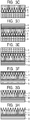
- an embodiment of the light-absorbing heat-shielding film of the present invention is a light-absorbing heat-shielding film which includes a metal layer 1 including fine irregularities 2 on its surface.
- a highly conductive metal is preferable as the material for the metal layer 1. Examples of highly conductive metals include silver, copper, gold, aluminum, magnesium, tungsten, cobalt, zinc, nickel, and chromium. Nickel, zinc, and chromium are preferable, and nickel is particularly preferable.
- the fine irregularities 2 provided on the surface of the metal layer 1 are also preferably made of the above highly conductive metal, and more preferably made of the same metal as the metal layer 1.
- a transparent metal oxide may be attached to the surface of the fine irregularities 2.
- the fine irregularities 2 are fine irregularities provided on one surface of the metal layer 1, and the height of the fine irregularities 2 refers to the difference in height between the apex of the convex portion and the bottom point of the concave portion formed on the surface of the metal layer.
- the average height of the fine irregularities 2 is 100 nm or more and 1000 nm or less, and preferably 100 nm or more and 500 nm or less.
- a transparent metal oxide may be attached to the surface of the fine irregularities 2.
- the average height of the fine irregularities 2 containing the transparent metal oxide is preferably 150 nm or more and 600 nm or less.
- the height of the fine irregularities 2 or the height of the fine irregularities 2 containing a transparent metal oxide refers to the difference in height between the top of the mountain and the bottom of the valley, as specified in JIS-B-061, "Definition and Indication of Surface Roughness," and is equivalent to the maximum roughness (Rmax).
- the light-absorbing heat-shielding film of the present invention have, on its surface, an average surface roughness Ra', which is a surface extension of the centerline average roughness Ra, of 1 nm or more and 50 nm or less.
- the average surface roughness Ra' value (nm) is the centerline average roughness Ra defined in JIS-B-0601, applied to the measurement surface and extended to three dimensions, and is expressed as "a value obtained by averaging the absolute values of deviation from the reference surface to the specified surface" and is obtained by the following formula (1).
- Ra ′ 1 S 0 ⁇ Y B Y T ⁇ X L X R F X Y ⁇ Z 0 d X d Y
- Ra' is the average surface roughness (nm)
- So is the area
- F(X, Y) is the height at the measurement point (X, Y) where the X-coordinate is X and the Y-coordinate is Y
- X L and X R are the range of the X-coordinate of the measurement surface
- Y B and Y T are the range of the Y-coordinate of the measurement surface
- Z 0 is the average height in the measurement surface.
- its surface preferably has a specific surface area Sr of 1.0 or more and 3.0 or less.
- So is the surface area where the measurement surface is ideally flat
- S is the surface area of the actual measurement surface.
- the surface area of the actual measured surface is determined by dividing the surface into micro triangles ⁇ ABC composed of three closest data points (A, B, and C), and then determining the area of each micro triangle ⁇ S using the vector product as described in formula (3) below. The sum of these ⁇ S is the surface area S to be determined.
- ⁇ S ⁇ ABC 2 s s ⁇ AB s ⁇ BC s ⁇ CA
- the height of the fine irregularities 2 can be determined by observing the cross section of the light-absorbing heat-shielding film of the present invention with a scanning electron microscope or the like.
- the average surface roughness Ra' and specific surface area of the surface of the light-absorbing heat-shielding film of the present invention can be determined by observing the surface of the metal layer including the fine irregularities by using a scanning probe microscope.
- Another embodiment of the light-absorbing heat-shielding film of the present invention may include a fine irregular shape 3 of a transparent metal oxide that is in close contact with the fine irregularities 2, as shown in FIG. 1B .
- another embodiment of the light-absorbing heat-shielding film of the present invention may further include a transparent metal oxide layer 4 that covers the surface of the fine irregular shape 3 of the metal oxide that is not in contact with the fine irregularities 2, as shown in FIG. 1C .
- close contact means that the metal oxide constituting the fine irregular shape 3 of the metal oxide fills the space surrounded by the fine irregularities 2 and reaches the metal layer 1.
- the average surface roughness Ra' which is a surface extension of the centerline average roughness Ra, on the surface of the metal oxide layer 4, which is the surface of the light-absorbing heat-shielding film
- the specific surface area Sr of the surface of the light-absorbing heat-shielding film is preferably 1.0 or more and 1.1 or less.
- the material of the fine irregular shape 3 of the metal oxide is not particularly limited, but it preferably contains alumina as a main component, and more preferably contains plate-shaped crystals containing alumina as a main component.
- the plate-shaped crystals containing alumina as a main component are formed of plate-shaped crystals containing an oxide or hydroxide of aluminum or a hydrate thereof as a main component, and a particularly preferable crystal is boehmite.
- the plate-shaped crystal containing alumina as a main component may be a plate-shaped crystal composed of only alumina, or may be a plate-shaped crystal containing a trace amount of zirconium, silicon, titanium, zinc, or the like in the plate-shaped crystal of alumina.
- the fine irregular shape 3 of the metal oxide By providing the fine irregular shape 3 of the metal oxide, it is possible to protect the fine irregularities 2. Further, when the fine irregular shape 3 of the metal oxide has a plate-shaped structure of plate-shaped crystals containing alumina as a main component, it is preferable that the plate-shaped crystals containing alumina as a main component be arranged in the direction perpendicular to the plane direction of the metal layer 1, and that the spatial occupancy of the fine irregular shape 3 continuously change.
- the material of the metal oxide layer 4 is not particularly limited, but preferably contains an amorphous gel of alumina.
- the metal oxide layer 4 increases the hardness of the surface of the light-absorbing heat-shielding film of the present invention, while lowering the light-absorbing property thereof. Therefore, the thickness of the metal oxide layer 4 may be appropriately determined so as to satisfy the required hardness and light-absorbing property.
- the aluminum elements, silicon elements, and the like in the fine irregularities 2, fine irregular shape 3, and metal oxide layer 4, as well as the metal elements such as silver, copper, gold, aluminum, magnesium, tungsten, cobalt, zinc, nickel, and chromium in the metal layer 1 can be detected by measurement such as energy dispersive X-ray analysis (EDX) or X-ray photoelectron spectroscopy (XPS) during surface or cross-sectional observation with a scanning electron microscope (SEM) or a transmission electron microscope (TEM).
- EDX energy dispersive X-ray analysis
- XPS X-ray photoelectron spectroscopy
- the ratio of metal oxides such as aluminum elements becomes lower and the ratio of metal elements constituting the metal layer 1 and fine irregularities 2 becomes higher, relatively in the direction perpendicular to the surface direction of the metal layer 1, from the surface (metal oxide layer 4) to the interior (metal layer 1), and finally only the metal elements are detected.
- the embodiment of the light-absorbing heat-shielding member of the present invention is a light-absorbing heat-shielding member in which a substrate 5 is provided on the surface of the metal layer 1 of the light-absorbing heat-shielding film of the present invention on the side opposite to the fine irregularities 2.
- the shape of the substrate 5 may be any shape as long as it can be formed according to the purpose of use, and examples thereof include, but are not limited to, a flat plate shape, a film shape, and a sheet shape.
- the material for the substrate 5 include, but are not limited to, metal, glass, ceramics, wood, paper, and resin.
- the resin examples include films and molded products of thermoplastic resins such as polyester, triacetyl cellulose, cellulose acetate, polyethylene terephthalate, polypropylene, polystyrene, polycarbonate, polymethyl methacrylate, ABS resin, polyphenylene oxide, polyurethane, polyethylene, and polyvinyl chloride; and thermosetting resins such as unsaturated polyester resins, phenolic resins, cross-linked polyurethane, cross-linked acrylic resins, and cross-linked saturated polyester resins.
- thermoplastic resins such as polyester, triacetyl cellulose, cellulose acetate, polyethylene terephthalate, polypropylene, polystyrene, polycarbonate, polymethyl methacrylate, ABS resin, polyphenylene oxide, polyurethane, polyethylene, and polyvinyl chloride
- thermosetting resins such as unsaturated polyester resins, phenolic resins, cross-linked polyurethane, cross-linked acrylic resins, and cross-linked saturated polyester resin
- the light-absorbing heat-shielding film and the substrate 5 may be bonded together with an adhesive layer 6.
- the adhesive layer 6 may be any layer as long as it can bond the light-absorbing heat-shielding film with the substrate 5, and examples thereof include a layer composed of a cured product of adhesive resin (for example, epoxy resin), double-sided tape, and the like.
- FIGS. 2A and 2B show a light-absorbing heat-shielding member provided with the light-absorbing heat-shielding film shown in FIG. 1C
- the light-absorbing heat-shielding member may be provided with the light-absorbing heat-shielding film shown in FIG. 1A or 1B instead of the light-absorbing heat-shielding film shown in FIG. 1C .
- a method of producing a light-absorbing heat-shielding film of the present invention includes a first step of forming a fine irregular shape of a metal oxide; and a second step of forming a metal layer on the fine irregular shape of the metal oxide.
- the light-absorbing heat-shielding member of the present invention further includes a step of bonding a substrate to a surface of the metal layer of the light-absorbing heat-shielding film opposite to a surface in contact with the fine irregular shape of the metal oxide.
- a fine irregular shape of a metal oxide to be used as a mold is formed.
- the material of the fine irregular shape of the metal oxide is not particularly limited, but preferably contains alumina as a main component.
- the fine irregular shape can be formed by a known vapor phase method such as chemical vapor deposition (CVD) or physical vapor deposition (PVD), or a sol-gel liquid phase method. With these methods, it is possible to provide a fine irregular shape of a metal oxide containing plate-shaped crystals containing alumina as a main component. Above all, a method of treating a film containing aluminum with warm water to grow alumina plate-shaped crystals is preferable.
- films containing aluminum examples include alumina gel films formed by applying a sol-gel coating solution containing aluminum compounds, and films containing metallic aluminum formed by dry film formation such as vacuum vapor deposition and sputtering. It is preferable to form a fine irregular shape of a metal oxide by using an alumina gel film from the viewpoints of the reactivity and easiness of adjusting the height of the fine irregular shape of the metal oxide.
- an aluminum compound such as an aluminum alkoxide, an aluminum halide, or an aluminum salt. From the viewpoint of film forming property, it is preferable to use aluminum alkoxide.
- Examples of the aluminum compound include aluminum alkoxides such as aluminum ethoxide, aluminum isopropoxide, aluminum-n-butoxide, aluminum-sec-butoxide, and aluminum-tert-butoxide, oligomers thereof, aluminum halides such as aluminum chloride, aluminum salts such as aluminum nitrate, aluminum acetate, aluminum phosphate, and aluminum sulfate, aluminum acetylacetonate, and aluminum hydroxide.
- aluminum alkoxides such as aluminum ethoxide, aluminum isopropoxide, aluminum-n-butoxide, aluminum-sec-butoxide, and aluminum-tert-butoxide, oligomers thereof, aluminum halides such as aluminum chloride, aluminum salts such as aluminum nitrate, aluminum acetate, aluminum phosphate, and aluminum sulfate, aluminum acetylacetonate, and aluminum hydroxide.
- the alumina gel film may contain an additional compound.
- the additional compound include alkoxides of zirconium, silicon, titanium, and zinc, halides, salts, and combinations thereof.
- the height of the fine irregular shape of the metal oxide formed can be made greater than in the case where none of these is contained.
- the alumina gel film is formed on a base substrate by applying a sol-gel coating solution containing an aluminum compound.
- the sol-gel coating solution is prepared by dissolving the aluminum compound in an organic solvent.
- the amount of the organic solvent is preferably about 20 times the amount of the aluminum compound in molar ratio.
- the organic solvent it is possible to use alcohol, carboxylic acid, aliphatic hydrocarbon, alicyclic hydrocarbon, aromatic hydrocarbon, ester, ketone, ether, or a mixed solvent thereof.
- the alcohol include methanol, ethanol, 2-propanol, butanol, 2-methoxyethanol, 2-ethoxyethanol, 1-methoxy-2-propanol, 1-ethoxy-2-propanol, 1-propoxy-2-propanol, 4-methyl-2-pentanol, 2-ethylbutanol, 3-methoxy-3-methylbutanol, ethylene glycol, diethylene glycol, and glycerin.
- carboxylic acid examples include n-butyric acid, ⁇ -methylbutyric acid, isovaleric acid, 2-ethylbutyric acid, 2,2-dimethylbutyric acid, 3,3-dimethylbutyric acid, 2,3-dimethylbutyric acid, 3-methylpentanoic acid, 4-methylpentanoic acid, 2-ethylpentanoic acid, 3-ethylpentanoic acid, 2,2-dimethylpentanoic acid, 3,3-dimethylpentanoic acid, 2,3-dimethylpentanoic acid, 2-ethylhexanoic acid, and 3-ethylhexanoic acid.
- Examples of the aliphatic hydrocarbon or alicyclic hydrocarbon include n-hexane, n-octane, cyclohexane, cyclopentane, and cyclooctane.
- Examples of the aromatic hydrocarbon include toluene, xylene, and ethylbenzene.
- Examples of the ester include ethyl formate, ethyl acetate, n-butyl acetate, ethylene glycol monomethyl ether acetate, ethylene glycol monoethyl ether acetate, and ethylene glycol monobutyl ether acetate.
- Examples of the ketone include acetone, methyl ethyl ketone, methyl isobutyl ketone, and cyclohexanone.
- Examples of the ether include dimethoxyethane, tetrahydrofuran, dioxane, and diisopropyl ether. Above all, it is preferable to use alcohol from the viewpoint of stability of the sol-gel coating solution.
- the aluminum alkoxide being highly reactive to water may cause rapid hydrolysis in contact with moisture in the air or with addition of water, resulting in clouding and precipitation in the sol-gel coating solution.
- a stabilizer it is possible to use ⁇ -diketone compounds, ⁇ -ketoester compounds, alkanolamines, and the like.
- ⁇ -diketone compounds examples include acetylacetone, trifluoroacetylacetone, hexafluoroacetylacetone, benzoylacetone, 3-methyl-2,4-pentanedione, and 3-ethyl-2,4-pentanedione.
- Examples of the ⁇ -ketoester compounds include methyl acetoacetate, ethyl acetoacetate, butyl acetoacetate, hexyl acetoacetate, allyl acetoacetate, benzyl acetoacetate, acetoacetic acid-iso-propyl, acetoacetic acid-2-methoxyethyl, acetoacetic acid-sec-butyl, acetoacetic acid-tert-butyl, and acetoacetic acid-iso-butyl.
- Examples of the alkanolamines include monoethanolamine, diethanolamine, and triethanolamine.
- the amount of the stabilizer is preferably about 1 time the amount of the aluminum alkoxide in molar ratio.
- a catalyst may be used to accelerate the hydrolysis reaction of the aluminum alkoxide.
- the catalyst include nitric acid, hydrochloric acid, sulfuric acid, phosphoric acid, acetic acid, and ammonia.
- a water-soluble organic polymer compound can be added to the alumina gel film as needed.
- the water-soluble organic polymer compound is easily eluted from the alumina gel film by immersion in warm water, which increases the reaction surface area between the aluminum compound and the warm water, enabling the formation of a fine irregular shape at low temperature and in a short time. Further, by changing the type and molecular weight of the organic polymer to be added, it is possible to control the height and the like of the formed fine irregular shape.
- the organic polymer polyether glycols such as polyethylene glycol and polypropylene glycol are preferable because they are easily eluted from the alumina gel film by immersion in warm water.
- the weight ratio of the amount of polyether glycols to the weight of the weight of the aluminum compound is preferably in the range of 0.1 to 10 times.
- a method for producing a fine irregular shape of a metal oxide is described with reference to FIGS. 3A and 3B .
- a sol-gel coating solution is prepared by dissolving or suspending an aluminum compound and, if necessary, additional compounds, a stabilizer, and a water-soluble organic polymer compound in an organic solvent. This sol-gel coating solution is applied onto the base substrate 8 and dried to form an alumina gel film as a film 7 containing aluminum. Alternatively, a film containing metallic aluminum as the film 7 containing aluminum is formed on the base substrate 8 by dry film formation such as vacuum vapor deposition or sputtering.
- the material for the base substrate 8 is not particularly limited, and various materials such as glass, plastic, and metal can be used.
- the atmosphere for application is an inert gas atmosphere such as dry air or dry nitrogen.
- the relative humidity in the dry atmosphere is preferably 30% or less.
- the solution application method for forming the alumina gel film it is possible to appropriately employ known application means such as a dipping method, a spin coating method, a spray method, a printing method, a flow coating method, and a combination thereof.
- the film thickness can be controlled by changing the pulling speed in the dipping method, the substrate rotation speed in the spin coating method, and the like, and changing the concentration of the sol-gel coating solution.
- the drying may be performed at room temperature for about 30 minutes.
- the preferable film thickness of the film 7 containing aluminum is 100 nm or more and 600 nm or less, preferably 100 nm or more and 300 nm or less, and more preferably 100 nm or more and 200 nm or less.
- the film 7 containing aluminum is subjected to immersion treatment in warm water to form a fine irregular shape of alumina.
- immersion treatment in warm water
- plate-shaped crystals containing alumina as the main component precipitate and grow on the surface layer of the alumina gel film due to the difference in solubility of various hydroxides in warm water, forming a fine irregular shape 3 of the metal oxide.
- the aluminum reacts with warm water and is oxidized to alumina, and then the fine irregular shape 3 of the metal oxide is formed as in the case of using the alumina gel film. Therefore, when the material of the base substrate 8 mainly contains aluminum or alumina, it is possible to omit the film formation of the film 7 containing aluminum on the base substrate 8.
- the temperature of the warm water is preferably 40°C or more and less than 100°C.
- the immersion treatment time is preferably about 5 minutes to 24 hours.
- the plate-shaped crystals of alumina are crystallized by using the difference in solubility of each component in warm water. Therefore, unlike the immersion treatment of the alumina gel film containing a single alumina component, the size of the plate-shaped crystals can be controlled over a wide range by changing the composition of the inorganic components. Further, the height of the fine irregular shape 3 of alumina can be adjusted by adjusting the film thickness of the film 7 containing aluminum.
- the average height of the fine irregular shape 3 of the metal oxide is preferably 100 nm or more and 1000 nm or less, and more preferably 100 nm or more and 500 nm or less. As a result, it becomes possible to control the fine irregularities formed by the plate-shaped crystals over the above-mentioned wide range.
- a metal layer is formed on the fine irregular shape of the metal oxide, and fine irregularities with the fine irregular shape transferred thereon are formed on the metal layer.
- the step of forming the metal layer 1 on the fine irregular shape 3 of the metal oxide is described below with reference to FIG. 3C .
- a metal plating treatment is preferable, and an electroless plating treatment is further preferable.
- an aqueous solution containing a palladium compound such as palladium chloride, a gold compound such as gold chloride, a silver compound such as silver chloride, or a tin compound such as tin chloride is applied to the fine irregular shape 3 of the metal oxide, followed by activation.
- the activation may be performed by immersing the fine irregular shape 3 of the metal oxide together with the base substrate 8 in an aqueous solution having a palladium compound dissolved therein. After that, the metal layer 1 is deposited on the fine irregular shape 3 of the metal oxide using an electroless plating solution.
- the metal ions in the electroless plating solution correspond to the metal layer of the light-absorbing heat-shielding film of the present invention, and an electroless plating solution containing nickel ions, chromium ions, or zinc ions is preferable, and a nickel-plating solution containing nickel ions is particularly preferable.
- the nickel-plating solution may contain a phosphorus component and a boron component in addition to the nickel component.
- Examples of commercially available nickel-plating solutions include the Top Nicoron series manufactured by Okuno Chemical Industries Co., Ltd.
- the temperature of the plating solution in the electroless plating treatment is preferably 30°C or more and 98°C or less, and more preferably 50°C or more and 90°C or less.
- the time for performing the electroless plating treatment can be adjusted according to the thickness of the metal layer to be formed, and is usually 30 seconds to 1 hour. In this way, the metal layer 1 is formed so as to fill the gaps of the fine irregular shape, and the metal layer 1 is formed including the fine irregularities 2 with the fine irregular shape 3 of the metal oxide transferred thereon.
- the thickness of the metal layer 1 including the fine irregularities 2 is 200 nm or more and 15000 nm or less.
- the average height of the fine irregularities 2 corresponds to the average height of the fine irregular shape 3 of the metal oxide, and is 100 nm or more and 1000 nm or less.
- the light-absorbing heat-shielding film of the present invention shows excellent light-absorbing and heat-shielding characteristics.
- electroplating treatment may be performed on the surface of the metal layer 1 opposite to the surface provided with the fine irregularities 2.
- a known electroplating solution can be used for the electroplating treatment.
- the electroplating treatment is performed using the same metal as the metal of the metal layer 1, the thickness of the metal layer can be increased by the electroplating treatment. Note that when the electroplating treatment is performed using a metal different from the metal of the metal layer 1, the metal layer provided by the electroplating treatment becomes the substrate 5.
- conductive salts, salts for adjusting counter ions, carboxylic acid-based additives for improving the homogeneity of the plating film, brightening agents, and the like may be added to the electroplating solution as necessary.
- the thickness of the metal layer 1 can be made a desired thickness by adjusting the solution temperature, current density, the plating time of the electroplating solution.
- an aqueous solution containing an acid or the like may be used for activation treatment of the surface of the metal layer 1 opposite to the surface provided with the fine irregularities 2.
- a step of removing foreign matters in the electroplating solution may be included.
- the substrate 5 is bonded to the surface of the metal layer 1 obtained above opposite to the surface provided with the fine irregularities 2.
- the shape and material of the substrate 5 those described above can be used.
- the metal as the substrate 5 may be further laminated on the surface of the metal layer 1 opposite to the surface provided with the fine irregularities 2.
- lamination may be performed by the above electroplating treatment, or lamination may be performed by physical vapor deposition such as sputtering.
- the substrate when the material of the substrate 5 is a resin, the substrate may be provided by depositing the resin as the substrate 5 on the surface of the metal layer 1 opposite to the fine irregular shape 3 of the metal oxide, followed by curing.
- the substrate 5 may be bonded to the metal layer 1 with the adhesive layer 6.
- the adhesive material used for the adhesive layer 6 is not particularly limited, and may be any material as long as the substrate 5 and the metal layer 1 are firmly bonded to each other.
- the etching step is described in detail using the example of a light-absorbing heat-shielding member including a substrate 5 and an adhesive layer 6 as shown in FIGS. 3E to 3H , but the same applies to a light-absorbing heat-shielding member including only the substrate 5 without the adhesive layer 6 and a light-absorbing heat-shielding film without the substrate 5 and the adhesive layer 6.
- FIG. 3E shows the light-absorbing heat-shielding member shown in FIG. 3D inverted upside down.
- the base substrate 8 is removed as shown in FIG. 3F .
- the light-absorbing heat-shielding member after removing the base substrate 8 includes a film 7 containing aluminum on the surface thereof.
- the film 7 containing aluminum is a film containing metallic aluminum
- visible light is reflected by the metallic aluminum, so that it is necessary to further remove the film containing metallic aluminum by etching, as shown in FIG. 3G .
- the film 7 containing aluminum is an alumina gel film
- the alumina gel film is the metal oxide layer 4 of the light-absorbing heat-shielding member.
- the alumina gel film may be removed by etching so as to satisfy the required surface hardness and light-absorbing property.
- etching method wet etching is preferable in which an acid or alkaline solution is used to dissolve the film 7 containing aluminum.
- the acid include hydrochloric acid, nitric acid, and sulfuric acid.
- the alkali include sodium hydroxide and potassium hydroxide. From the viewpoint of work efficiency, an etching method using an alkaline solution is more preferable.
- the etching concentration is preferably in the range of several percent to several tens of percent, and the etching time is preferably in the range of several hours to several days. Further, as shown in FIG.
- the fine irregular shape 3 of the metal oxide may also be removed by etching.
- the light-absorbing heat-shielding member in which the metal layer 1 including the fine irregularities 2 on the outermost surface is bonded to the substrate 5 via the adhesive layer 6 achieves particularly excellent light-absorbing property.
- the residual metal oxide such as alumina after etching can be detected, for example, by measuring EDX or XPS when observing the surface or cross section by SEM or TEM.
- the degree of the etching treatment may be adjusted according to the balance between the light-absorbing property and the surface hardness of the desired light-absorbing heat-shielding member or light-absorbing heat-shielding film. Further, prior to performing the substrate adhesion step as the third step, the etching step of this step may be performed, and after that the substrate may be bonded.
- the light-absorbing heat-shielding member and the light-absorbing heat-shielding film of the present invention include the metal layer 1 including fine irregularities 2, so that the reflective index in the visible light region is low because they absorb visible light, and the reflective index in the far-infrared region is high because they emit less far-infrared rays, thus achieving excellent light-absorbing and heat-shielding characteristics.
- the light-absorbing heat-shielding film of the present invention By providing the light-absorbing heat-shielding film of the present invention on the surface of various members or articles, the light-absorbing heat-shielding member can be obtained.
- the light-absorbing heat-shielding film of the present invention is preferably used for a heating element as a member or an article. Examples of the article provided with such a heating element include a battery, an engine, a motor, and a vehicle.
- the light-absorbing heat-shielding film of the present invention can also be used for clothes and the like. Further, the light-absorbing heat-shielding film of the present invention may be used as a heat-shielding decorative film.
- the light-absorbing heat-shielding film of the present invention can be provided as a heat-shielding decorative film on the surface of vehicle interiors, mobile devices, home appliances, parasols, and tent supplies.
- Various adhesives can be used when the light-absorbing heat-shielding film of the present invention is provided on the surface of a member or an article. Therefore, the light-absorbing heat-shielding film of the present invention can be provided on the surfaces of members and articles according to the purpose of use, and the surfaces of members and articles are not limited to those that are smooth, and may have a two-dimensional or three-dimensional curved surface.
- the member or article provided with the light-absorbing heat-shielding film of the present invention on the outermost surface causes a difference in detected temperature as compared with the member or article not provided with the light-absorbing heat-shielding film, and therefore, by using the light-absorbing heat-shielding film of the present invention, it is possible to clearly identify the member or article.
- the detected temperature on the surface of the light-absorbing heat-shielding film opposite to the surface in contact with the member or article may be lower by 3°C or more than the detected temperature on the portion of the member or article not provided with the light-absorbing heat-shielding film.
- the member or article is a heating element, it can be identified more clearly.
- a lens reflective index measuring device (trade name: USPM-RU III, manufactured by Olympus Corporation) was used for the reflective index spectrum measurement in the visible light regions of Examples.
- a Fourier transform infrared spectrophotometer (FT/IR-6600, manufactured by JASCO Corporation) was used for the reflective index spectrum measurement in the infrared region of the examples.
- An alumina sol solution was prepared by dissolving aluminum-sec-butoxide (hereinafter also referred to as “Al(O-sec-Bu) 3 ”) and ethyl acetoacetate (hereinafter also referred to as "EtOAcAc”) in 2-propanol (hereinafter also referred to as "IPA”) and stirring at room temperature for about 3 hours.
- Al(O-sec-Bu) 3 aluminum-sec-butoxide
- EtOAcAc ethyl acetoacetate
- IPA 2-propanol
- a 0.01 M dilute aqueous solution of hydrochloric acid was added to the alumina sol solution so that the amount of hydrochloric acid added was twice the molar ratio of Al(O-sec-Bu) 3 , and the mixture was refluxed for about 6 hours to prepare a sol-gel coating solution.
- the sol-gel coating solution was applied onto a quartz glass substrate as the base substrate by the spin coating method to form a coating film. After that, the coating film was heat-treated at 100°C for 1 hour to obtain a transparent alumina gel film. Next, the alumina gel film was immersed in warm water at 80°C for 30 minutes and then dried at 100°C for 10 minutes to form an alumina layer having a fine irregular shape.
- An aqueous solution of palladium chloride was applied on the alumina layer having a fine irregular shape by the spin coating method, and then dried at 100°C. After that, it was subjected to immersion treatment in a nickel-phosphorus plating solution set at 80°C (phosphorus content of about 10 wt%) for 1 minute to form fine irregularities and a nickel layer as a metal layer.
- An epoxy-based resin as an adhesive layer was applied to the surface of the obtained metal layer opposite to the alumina layer having a fine irregular shape, cured, and a PET film as a substrate was bonded with the adhesive layer. After that, the light-absorbing heat-shielding member was released from the quartz glass substrate together with the substrate to produce the light-absorbing heat-shielding member.
- a nickel layer was formed on the alumina layer having a fine irregular shape, which was cut out with a dicing saw, and then thinned in the cross-sectional direction by the focused ion beam (FIB) method, and the cross section was observed by SEM.
- the cross section was observed using a scanning transmission electron microscope (trade name: HD-2300, manufactured by Hitachi High-Technologies Corporation). From the observation image shown in FIG. 4 , fine irregularities 2 are formed to fill the inside of the alumina plate-shaped crystals, which have a fine irregular shape 3 of the metal oxide formed from the alumina gel film on the base substrate 8, and a nickel layer as the metal layer 1 is present on top of the fine irregularities 2.
- the average height of the fine irregularities 2 of the obtained light-absorbing heat-shielding member was 323 nm, the average height of the fine irregular shape 3 was 255 nm, and the film thickness of the film 7 containing aluminum was 68 nm.
- the average surface roughness Ra' was 1.0 nm, and the specific surface area was 1.0.
- the reflective index spectrum in the visible light region and the reflective index spectrum in the infrared region were measured.
- the reflective index spectrum was measured using a lens reflective index measuring device (trade name: USPM-RU III, manufactured by Olympus Corporation), and the reflective index spectrum in the infrared region was measured using a Fourier transform infrared spectrophotometer (trade name: FT/IR-6600, manufactured by JASCO Corporation).
- FIG. 5 shows the result of the reflective index spectrum measurement in the visible light region
- FIG. 6 shows the result of the reflective index spectrum measurement in the infrared region.
- Table 1 shows the reflective indices in the visible light and infrared regions obtained by measuring the reflective index spectra in the visible light region and the infrared region of the light-absorbing heat-shielding member. From FIG. 5 , it can be said that the light-absorbing heat-shielding member of the present invention has an excellent light-absorbing property because the reflective index in the visible light region is low.
- the light-absorbing heat-shielding member of the present invention has an excellent heat-shielding property because the reflective index increases toward the long wavelength side in the mid-infrared and far-infrared regions.
- the reflective index spectrum in the visible light region and the reflective index spectrum in the infrared region were measured under the same conditions as the light-absorbing heat-shielding member of Example 1.
- FIG. 5 , FIG. 6 , and Table 1 show the results.
- the light-absorbing material of Comparative Example 1 is inferior to the light-absorbing heat-shielding member of Example 1, it can be said that the reflective index in the visible light to near-infrared regions is low and the light-absorbing property is excellent.
- the light-absorbing material of Comparative Example 1 is inferior in reflective index in the mid-infrared region and the far-infrared region compared to the light-absorbing heat-shielding member of the present invention, and cannot be said to have a heat-shielding property.
- an alumina sol solution was prepared and used for the application onto a quartz glass substrate as the base substrate by the spin coating method to form a coating film. After that, the coating film was heat-treated at 100°C for 1 hour to obtain a transparent alumina gel film. Next, the alumina gel film was immersed in warm water at 80°C for 30 minutes and then dried at 100°C for 10 minutes to form an alumina layer having a fine irregular shape.
- An aqueous solution of palladium chloride was applied on the alumina layer having a fine irregular shape by the spin coating method, and then dried at room temperature. After that, it was subjected to immersion treatment in a nickel-phosphorus plating solution set at 80°C (phosphorus content of about 10 wt%) for 20 minutes to form fine irregularities and a nickel layer as a metal layer.
- the light-absorbing heat-shielding film was released from the quartz glass substrate.
- the total film thickness of the obtained light-absorbing heat-shielding film was about 10 ⁇ m.
- the average height of the fine irregularities of the light-absorbing heat-shielding film was 303 nm, the average height of the fine irregular shape was 233 nm, and the film thickness of the film containing aluminum was 70 nm.
- the average surface roughness Ra' was 1.0 nm, and the specific surface area was 1.0.
- a light-absorbing heat-shielding film was produced in the same manner as in Example 2, and as an etching step, the light-absorbing heat-shielding film released from the quartz glass substrate was subjected to etching treatment with a 3 M sodium hydroxide aqueous solution at room temperature for 50 hours to produce a light-absorbing heat-shielding film. A small amount of transparent metal oxide was attached to the fine irregularities after etching.
- the average height of the fine irregularities containing the transparent metal oxide of the obtained light-absorbing heat-shielding film was 251 nm, and the average height of the fine irregularities was 213 nm, and on the surface of the light-absorbing heat-shielding film, the average surface roughness Ra' was 5.0 nm, and the specific surface area was 1.1.
- FIG. 5 shows the result of the reflective index spectrum measurement in the visible light region
- FIG. 6 shows the result of the reflective index spectrum measurement in the infrared region.
- the cross section was obtained by the FIB method, and the cross section was observed by SEM. The cross section was observed using a scanning electron microscope (trade name: ULTRA 55, manufactured by Carl Zeiss). From the observation image shown in FIG.
- nickel fine irregularities 2 were formed on the nickel layer as the metal layer 1, and a trace amount of alumina remained on the fine irregularities 2.
- the proportion of Al element was relatively low, while the proportion of Ni element was high, from the surface toward the inside in the film thickness direction of the cross section.
- a light-absorbing heat-shielding film was produced in the same manner as in Example 3 except that the etching treatment was performed in the etching step using a 7.5 M sodium hydroxide aqueous solution at room temperature for 47 hours.
- the average height of the fine irregularities of the obtained light-absorbing heat-shielding film was 235 nm, and on the surface of the light-absorbing heat-shielding film, the average surface roughness Ra' was 18 nm, and the specific surface area was 1.4.
- a light-absorbing heat-shielding film was produced in the same manner as in Example 3 except that a nickel-phosphorus plating solution (phosphorus content of about 1 to 2 wt%) was used as the plating solution.
- the average height of the fine irregularities of the obtained light-absorbing heat-shielding film was 272 nm, and on the surface of the light-absorbing heat-shielding film, the average surface roughness Ra' was 3.8 nm, and the specific surface area was 1.1.
- the alumina sol solution shown in Example 2 was prepared and applied onto a quartz glass substrate as the base substrate by the spin coating method to form a coating film. After that, the coating film was heat-treated at 100°C for 1 hour, and further, the film coating and the film drying process were repeated to obtain a transparent alumina gel film as a film containing aluminum with two layers of laminates. Thereafter, a light-absorbing heat-shielding film was produced in the same manner as in Example 2.
- the average height of the fine irregularities of the obtained light-absorbing heat-shielding film was 306 nm, and the average height of the fine irregular shape was 371 nm, and on the surface of the light-absorbing heat-shielding film, the average surface roughness Ra' was 1.1 nm and the specific surface area was 1.0.
- a light-absorbing heat-shielding film was produced in the same manner as in Example 6 except that after releasing the metal film provided with an alumina layer from the quartz glass substrate, an etching treatment was performed at room temperature for 50 hours using a 3 M sodium hydroxide aqueous solution as the etching step.
- the average height of the fine irregularities of the obtained light-absorbing heat-shielding film was 315 nm, and on the surface of the light-absorbing heat-shielding film, the average surface roughness Ra' was 10 nm, and the specific surface area was 1.2.
- a light-absorbing heat-shielding film was produced in the same manner as in Example 7 except that the etching treatment was performed in the etching step using a 7.5 M sodium hydroxide aqueous solution at room temperature for 50 hours.
- the average height of the fine irregularities of the obtained light-absorbing heat-shielding film was 303 nm, and on the surface of the light-absorbing heat-shielding film, the average surface roughness Ra' was 27 nm, and the specific surface area was 1.7.
- a light-absorbing heat-shielding film was produced in the same manner as in Example 2 except that the number of laminated alumina gel films was three.
- the average height of the fine irregularities of the obtained light-absorbing heat-shielding film was 374 nm, and the average height of the fine irregular shape was 419 nm, and on the surface of the light-absorbing heat-shielding film, the average surface roughness Ra' was 1.2 nm, and the specific surface area was 1.0.
- a light-absorbing heat-shielding film was produced in the same manner as in Example 9 except that after releasing the metal film provided with an alumina layer from the quartz glass substrate, an etching treatment was performed at room temperature for 50 hours using a 3 M sodium hydroxide aqueous solution in the etching step.
- the average height of the fine irregularities of the obtained light-absorbing heat-shielding film was 354 nm, and on the surface of the light-absorbing heat-shielding film, the average surface roughness Ra' was 16 nm, and the specific surface area was 1.3.
- a light-absorbing heat-shielding film was produced in the same manner as in Example 10 except that the etching treatment was performed in the etching step using a 6 M sodium hydroxide aqueous solution at room temperature for 45 hours.
- the average height of the fine irregularities of the obtained light-absorbing heat-shielding film was 346 nm, and on the surface of the light-absorbing heat-shielding film, the average surface roughness Ra' was 35 nm, and the specific surface area was 2.1.
- Table 1 shows the reflective index in the visible light region and infrared region obtained by measuring the reflective index spectra in the visible light region and infrared region of the light-absorbing heat-shielding films or light-absorbing heat-shielding members produced in Examples 1 to 11 and Comparative Example 1.
- An article was prepared in which the light-absorbing heat-shielding film produced in Example 3 was attached to the surface of a plate-shaped stainless steel (SUS) (hereinafter referred to as "article including a light-absorbing heat-shielding film”).
- An article including a light-absorbing heat-shielding film and an article same as the article having a light-absorbing heat-shielding film on the surface except for not having a light-absorbing heat-shielding film (hereinafter referred to as "article not provided with a light-absorbing heat-shielding film") were placed on a heater, and when the surface temperature of the article not provided with a light-absorbing heat-shielding film reached 40°C, an infrared thermography device (model: H2640, manufactured by Nippon Avionics Co., Ltd.) was used to measure the surface temperature of the article including a light-absorbing heat-shielding film and the article not provided with a light-absorbing heat-shielding film.
- the surface temperature measurement environment was room temperature, and the distance between the article and the measuring device was about 40 cm.
- the surface temperature of the article including a light-absorbing heat-shielding film was about 28°C, which was lower by about 12°C than the surface temperature of the article not provided with a light-absorbing heat-shielding film.
- the surface temperature of the article not provided with a light-absorbing heat-shielding film was about 60°C
- the surface temperature of the article including a light-absorbing heat-shielding film was about 37°C, which was about 23°C lower. From the above, it was found that the light-absorbing heat-shielding film of the present invention had an excellent heat-shielding property. A clear temperature difference was observed when the detected temperature of the article was compared with the actual temperature, and it was found that the article could be identified with an infrared thermal image camera.
- An article including a light-absorbing heat-shielding film was prepared by attaching the light-absorbing heat-shielding film produced in Example 5 to the surface of a plate-shaped stainless steel, and in the same manner as in Example 12, the surface temperatures of the article including a light-absorbing heat-shielding film and the article not provided with a light-absorbing heat-shielding film were measured.
- the surface temperature of the article not provided with a light-absorbing heat-shielding film was about 40°C
- the surface temperature of the article including a light-absorbing heat-shielding film was about 28°C, which was lower by about 12°C than the surface temperature of the article not provided with a light-absorbing heat-shielding film.
- the surface temperature of the article not provided with a light-absorbing heat-shielding film was about 60°C
- the surface temperature of the article including a light-absorbing heat-shielding film was about 33°C, which was about 27°C lower.
- the part of the present invention is excellent in both light-absorbing property and heat-shielding property.
- the present invention can provide a light-absorbing heat-shielding film and a light-absorbing heat-shielding member that absorb visible light and near-infrared rays (low reflective index) and emit less far-infrared rays (high reflective index), which are usually incompatible.
- the light-absorbing heat-shielding film and the light-absorbing heat-shielding member can be used as stray light prevention and heat-shielding members inside optical equipment, as interior and exterior members of space-related equipment such as satellites, as exterior films, and as solar collectors.
Landscapes
- Chemical & Material Sciences (AREA)
- Engineering & Computer Science (AREA)
- Mechanical Engineering (AREA)
- Organic Chemistry (AREA)
- Metallurgy (AREA)
- Chemical Kinetics & Catalysis (AREA)
- Materials Engineering (AREA)
- Inorganic Chemistry (AREA)
- General Chemical & Material Sciences (AREA)
- Physics & Mathematics (AREA)
- Thermal Sciences (AREA)
- General Physics & Mathematics (AREA)
- Optics & Photonics (AREA)
- Dispersion Chemistry (AREA)
- Ceramic Engineering (AREA)
- Laminated Bodies (AREA)
- Other Surface Treatments For Metallic Materials (AREA)
Abstract
Description
- The present invention relates to a light-absorbing heat-shielding film, a light-absorbing heat-shielding member, and an article, as well as a method of producing the same.
- In recent years, the use of heat-shielding materials to suppress temperature rise has been expanding in the interior and exterior parts of optical equipment, space equipment, and transportation products. In addition, materials having both a light-absorbing property and a heat-shielding property are required because heat-shielding materials also having a light-absorbing property can reduce noise caused by stray light when used inside the lens barrels of infrared cameras or in aperture films, and also achieve high dimensional stability owing to the property of not easily rising in temperature. Conventionally, as light-absorbing materials, light-absorbing materials with black electroless nickel plating have been known (for example, NPL 1). This is a light-absorbing material in which a nickel plating on the surface of an object is oxidized to be formed into a fine irregular shape, thereby blackening the surface. In addition, a technique has been shown to fabricate a resin with a microstructure on its surface by injection molding using a mold with a metal surface having a fine irregular shape (PTL 1).
- PTL 1:
Japanese Patent Application Laid-Open No. 2004-261910 - NPL 1: "Black Electroless Nickel Plating", Journal of the Surface Finishing Society of Japan, Vol. 66, No. 11, 503-506, 2015
- However, the black-colored material disclosed in the
above NPL 1 emits a large amount of radiation even in the far-infrared region and does not exhibit an excellent heat-shielding property. In addition, the invention described inPTL 1 relates to an injection molding of resin using a mold, and is incapable of molding a metal film in a versatile form. For this reason, it is difficult to apply members thus obtained to various products as light-absorbing heat-shielding members, which poses problem in practical use. - The present invention has been made in view of the above problems, and an object thereof is to provide a light-absorbing heat-shielding member having usually incompatible characteristics of absorbing visible light and near-infrared rays (that is, low reflective index) and emitting less far-infrared rays (that is, high reflective index).
- A light-absorbing heat-shielding film according to the present invention includes a metal layer including fine irregularities, wherein a height of the fine irregularities is 100 nm or more and 1000 nm or less.
- According to the present invention, use of a light-absorbing heat-shielding film with fine irregularities makes it possible to achieve light-absorbing and heat-shielding characteristics, which are usually incompatible. In addition, when a light-absorbing heat-shielding film of the present invention is placed on a surface of a heat-generating member, the detected temperature can be lowered by about 3°C or more.
-
- [
FIG. 1A ]
FIG. 1A is a schematic diagram showing an embodiment of the light-absorbing heat-shielding film of the present invention. - [
FIG. 1B ]
FIG. 1B is a schematic diagram showing an embodiment of the light-absorbing heat-shielding film of the present invention. - [
FIG. 1C ]
FIG. 1C is a schematic diagram showing an embodiment of the light-absorbing heat-shielding film of the present invention. - [
FIG. 2A ]
FIG. 2A is a schematic diagram showing an embodiment of the light-absorbing heat-shielding member of the present invention. - [
FIG. 2B ]
FIG. 2B is a schematic diagram showing an embodiment of the light-absorbing heat-shielding member of the present invention. - [
FIG. 3A ]
FIG. 3A is a process diagram showing an embodiment of the method of producing a light-absorbing heat-shielding member of the present invention. - [
FIG. 3B ]
FIG. 3B is a process diagram showing an embodiment of the method of producing a light-absorbing heat-shielding member of the present invention. - [
FIG. 3C ]
FIG. 3C is a process diagram showing an embodiment of the method of producing a light-absorbing heat-shielding member of the present invention. - [
FIG. 3D ]
FIG. 3D is a process diagram showing an embodiment of the method of producing a light-absorbing heat-shielding member of the present invention. - [
FIG. 3E ]
FIG. 3E is a process diagram showing an embodiment of the method of producing a light-absorbing heat-shielding member of the present invention. - [
FIG. 3F ]
FIG. 3F is a process diagram showing an embodiment of the method of producing a light-absorbing heat-shielding member of the present invention. - [
FIG. 3G ]
FIG. 3G is a process diagram showing an embodiment of the method of producing a light-absorbing heat-shielding member of the present invention. - [
FIG. 3H ]
FIG. 3H is a process diagram showing an embodiment of the method of producing a light-absorbing heat-shielding member of the present invention. - [
FIG. 4 ]
FIG. 4 is an electron microscope observation view of a cross section of the light-absorbing heat-shielding member obtained in Example 1. - [
FIG. 5 ]
FIG. 5 shows measurement results of the reflective index spectra in the visible light region of the light-absorbing heat-shielding members obtained in Examples 1 and 3 and the light-absorbing member obtained in Comparative Example 1. - [
FIG. 6 ]
FIG. 6 shows measurement results of the reflective index spectra in the infrared region of the light-absorbing heat-shielding members obtained in Examples 1 and 3 and the light-absorbing member obtained in Comparative Example 1. - [
FIG. 7 ]
FIG. 7 is an electron microscope observation view of a cross section of the light-absorbing heat-shielding member obtained in Example 3. - Hereinafter, embodiments of the present invention are described in detail.
- A light-absorbing heat-shielding film according to the present invention includes a metal layer including fine irregularities, wherein a height of the fine irregularities is 100 nm or more and 1000 nm or less.
- Highly conductive metals such as aluminum and nickel emit less far-infrared rays and have a heat-shielding property, but do not show a light-absorbing property. On the other hand, fine irregular shapes with sub-wavelength structures smaller than the wavelengths of visible light are known to have anti-reflection effects, and to exhibit excellent wavelength band characteristics and incident angle characteristics when the spatial occupancy of the structure is continuously changed. Therefore, when the metal surface is made into fine irregularities, the reflection on the metal surface is suppressed in a wide wavelength region of visible light, the reflective index in the entire visible light region is lowered, so that the surface looks black and exhibits a light-absorbing property. Therefore, it is considered that a metal member having a fine irregular shape structure on its surface can have both light-absorbing and heat-shielding properties. However, the light-absorbing material disclosed in
NPL 1 has a fine irregular shape on its surface obtained by oxidizing the nickel surface, but it emits a large amount of radiation (low reflective index) even in the far-infrared region and does not exhibit a heat-shielding property. Therefore, the present inventors found that, in addition to the heat-shielding property of the metal itself that forms the light-absorbing heat-shielding film, the specific shape of the fine irregular shape on the metal surface was important for the exhibition of the heat-shielding property. Thus, the present invention was completed. - Specifically, including specific fine irregularities provided on the metal layer, the light-absorbing heat-shielding film of the present invention can exhibit both light-absorbing property and heat-shielding property. In particular, the light-absorbing heat-shielding film of the present invention preferably has a reflective index of 10% or less in the visible light region (550 nm) and a reflective index of 70% or more in the far-infrared light region (10 µm).
- The light-absorbing heat-shielding film of the present invention is described with reference to
FIGS. 1A to 1C . As shown inFIG. 1A , an embodiment of the light-absorbing heat-shielding film of the present invention is a light-absorbing heat-shielding film which includes ametal layer 1 includingfine irregularities 2 on its surface. A highly conductive metal is preferable as the material for themetal layer 1. Examples of highly conductive metals include silver, copper, gold, aluminum, magnesium, tungsten, cobalt, zinc, nickel, and chromium. Nickel, zinc, and chromium are preferable, and nickel is particularly preferable. Thefine irregularities 2 provided on the surface of themetal layer 1 are also preferably made of the above highly conductive metal, and more preferably made of the same metal as themetal layer 1. In addition, a transparent metal oxide may be attached to the surface of thefine irregularities 2. - The
fine irregularities 2 are fine irregularities provided on one surface of themetal layer 1, and the height of thefine irregularities 2 refers to the difference in height between the apex of the convex portion and the bottom point of the concave portion formed on the surface of the metal layer. The average height of thefine irregularities 2 is 100 nm or more and 1000 nm or less, and preferably 100 nm or more and 500 nm or less. Further, a transparent metal oxide may be attached to the surface of thefine irregularities 2. The average height of thefine irregularities 2 containing the transparent metal oxide is preferably 150 nm or more and 600 nm or less. Here, the height of thefine irregularities 2 or the height of thefine irregularities 2 containing a transparent metal oxide refers to the difference in height between the top of the mountain and the bottom of the valley, as specified in JIS-B-061, "Definition and Indication of Surface Roughness," and is equivalent to the maximum roughness (Rmax). In addition, it is preferable that the light-absorbing heat-shielding film of the present invention have, on its surface, an average surface roughness Ra', which is a surface extension of the centerline average roughness Ra, of 1 nm or more and 50 nm or less. Here, the average surface roughness Ra' value (nm) is the centerline average roughness Ra defined in JIS-B-0601, applied to the measurement surface and extended to three dimensions, and is expressed as "a value obtained by averaging the absolute values of deviation from the reference surface to the specified surface" and is obtained by the following formula (1).
[Math. 1]
- In the formula (1), Ra' is the average surface roughness (nm), So is the area |XR-XL|×|YT-YB| where the measurement surface is ideally flat, F(X, Y) is the height at the measurement point (X, Y) where the X-coordinate is X and the Y-coordinate is Y, XL and XR are the range of the X-coordinate of the measurement surface, YB and YT are the range of the Y-coordinate of the measurement surface, and Z0 is the average height in the measurement surface.
- Further, in the light-absorbing heat-shielding film of the present invention, its surface preferably has a specific surface area Sr of 1.0 or more and 3.0 or less. The specific surface area Sr is calculated by the following formula (2).

- In the formula (2), So is the surface area where the measurement surface is ideally flat, and S is the surface area of the actual measurement surface.
- Note that the surface area of the actual measured surface is determined by dividing the surface into micro triangles ΔABC composed of three closest data points (A, B, and C), and then determining the area of each micro triangle ΔS using the vector product as described in formula (3) below. The sum of these ΔS is the surface area S to be determined.

- In the formula (3), AB, BC, and CA are the lengths of the respective sides, and 2s=AB+BC+CA.
- The height of the
fine irregularities 2 can be determined by observing the cross section of the light-absorbing heat-shielding film of the present invention with a scanning electron microscope or the like. In addition, the average surface roughness Ra' and specific surface area of the surface of the light-absorbing heat-shielding film of the present invention can be determined by observing the surface of the metal layer including the fine irregularities by using a scanning probe microscope. - Another embodiment of the light-absorbing heat-shielding film of the present invention may include a fine
irregular shape 3 of a transparent metal oxide that is in close contact with thefine irregularities 2, as shown inFIG. 1B . In addition, another embodiment of the light-absorbing heat-shielding film of the present invention may further include a transparentmetal oxide layer 4 that covers the surface of the fineirregular shape 3 of the metal oxide that is not in contact with thefine irregularities 2, as shown inFIG. 1C . Here, close contact means that the metal oxide constituting the fineirregular shape 3 of the metal oxide fills the space surrounded by thefine irregularities 2 and reaches themetal layer 1. Note that when the light-absorbing heat-shielding film includes a fineirregular shape 3 and ametal oxide layer 4, the average surface roughness Ra', which is a surface extension of the centerline average roughness Ra, on the surface of themetal oxide layer 4, which is the surface of the light-absorbing heat-shielding film, is preferably 1 nm or more and 4 nm or less, and the specific surface area Sr of the surface of the light-absorbing heat-shielding film is preferably 1.0 or more and 1.1 or less. - The material of the fine
irregular shape 3 of the metal oxide is not particularly limited, but it preferably contains alumina as a main component, and more preferably contains plate-shaped crystals containing alumina as a main component. The plate-shaped crystals containing alumina as a main component are formed of plate-shaped crystals containing an oxide or hydroxide of aluminum or a hydrate thereof as a main component, and a particularly preferable crystal is boehmite. Here, the plate-shaped crystal containing alumina as a main component may be a plate-shaped crystal composed of only alumina, or may be a plate-shaped crystal containing a trace amount of zirconium, silicon, titanium, zinc, or the like in the plate-shaped crystal of alumina. - By providing the fine
irregular shape 3 of the metal oxide, it is possible to protect thefine irregularities 2. Further, when the fineirregular shape 3 of the metal oxide has a plate-shaped structure of plate-shaped crystals containing alumina as a main component, it is preferable that the plate-shaped crystals containing alumina as a main component be arranged in the direction perpendicular to the plane direction of themetal layer 1, and that the spatial occupancy of the fineirregular shape 3 continuously change. - The material of the
metal oxide layer 4 is not particularly limited, but preferably contains an amorphous gel of alumina. Themetal oxide layer 4 increases the hardness of the surface of the light-absorbing heat-shielding film of the present invention, while lowering the light-absorbing property thereof. Therefore, the thickness of themetal oxide layer 4 may be appropriately determined so as to satisfy the required hardness and light-absorbing property. - The aluminum elements, silicon elements, and the like in the
fine irregularities 2, fineirregular shape 3, andmetal oxide layer 4, as well as the metal elements such as silver, copper, gold, aluminum, magnesium, tungsten, cobalt, zinc, nickel, and chromium in themetal layer 1 can be detected by measurement such as energy dispersive X-ray analysis (EDX) or X-ray photoelectron spectroscopy (XPS) during surface or cross-sectional observation with a scanning electron microscope (SEM) or a transmission electron microscope (TEM). When thefine irregularities 2, the fineirregular shape 3, or themetal oxide layer 4 is provided, the ratio of metal oxides such as aluminum elements becomes lower and the ratio of metal elements constituting themetal layer 1 andfine irregularities 2 becomes higher, relatively in the direction perpendicular to the surface direction of themetal layer 1, from the surface (metal oxide layer 4) to the interior (metal layer 1), and finally only the metal elements are detected. - As shown in
FIG. 2A , the embodiment of the light-absorbing heat-shielding member of the present invention is a light-absorbing heat-shielding member in which asubstrate 5 is provided on the surface of themetal layer 1 of the light-absorbing heat-shielding film of the present invention on the side opposite to thefine irregularities 2. The shape of thesubstrate 5 may be any shape as long as it can be formed according to the purpose of use, and examples thereof include, but are not limited to, a flat plate shape, a film shape, and a sheet shape. Examples of the material for thesubstrate 5 include, but are not limited to, metal, glass, ceramics, wood, paper, and resin. Examples of the resin include films and molded products of thermoplastic resins such as polyester, triacetyl cellulose, cellulose acetate, polyethylene terephthalate, polypropylene, polystyrene, polycarbonate, polymethyl methacrylate, ABS resin, polyphenylene oxide, polyurethane, polyethylene, and polyvinyl chloride; and thermosetting resins such as unsaturated polyester resins, phenolic resins, cross-linked polyurethane, cross-linked acrylic resins, and cross-linked saturated polyester resins. - As shown in
FIG. 2B , in another embodiment of the present invention, the light-absorbing heat-shielding film and thesubstrate 5 may be bonded together with anadhesive layer 6. Theadhesive layer 6 may be any layer as long as it can bond the light-absorbing heat-shielding film with thesubstrate 5, and examples thereof include a layer composed of a cured product of adhesive resin (for example, epoxy resin), double-sided tape, and the like. - Note that although
FIGS. 2A and 2B show a light-absorbing heat-shielding member provided with the light-absorbing heat-shielding film shown inFIG. 1C , the light-absorbing heat-shielding member may be provided with the light-absorbing heat-shielding film shown inFIG. 1A or 1B instead of the light-absorbing heat-shielding film shown inFIG. 1C . - Hereinafter, a method of producing the light-absorbing heat-shielding film and the light-absorbing heat-shielding member of the present invention is described with reference to
FIGS. 3A to 3H . - A method of producing a light-absorbing heat-shielding film of the present invention includes a first step of forming a fine irregular shape of a metal oxide; and a second step of forming a metal layer on the fine irregular shape of the metal oxide. The light-absorbing heat-shielding member of the present invention further includes a step of bonding a substrate to a surface of the metal layer of the light-absorbing heat-shielding film opposite to a surface in contact with the fine irregular shape of the metal oxide.
- In the first step, a fine irregular shape of a metal oxide to be used as a mold is formed.
- The material of the fine irregular shape of the metal oxide is not particularly limited, but preferably contains alumina as a main component. The fine irregular shape can be formed by a known vapor phase method such as chemical vapor deposition (CVD) or physical vapor deposition (PVD), or a sol-gel liquid phase method. With these methods, it is possible to provide a fine irregular shape of a metal oxide containing plate-shaped crystals containing alumina as a main component. Above all, a method of treating a film containing aluminum with warm water to grow alumina plate-shaped crystals is preferable.
- Examples of films containing aluminum include alumina gel films formed by applying a sol-gel coating solution containing aluminum compounds, and films containing metallic aluminum formed by dry film formation such as vacuum vapor deposition and sputtering. It is preferable to form a fine irregular shape of a metal oxide by using an alumina gel film from the viewpoints of the reactivity and easiness of adjusting the height of the fine irregular shape of the metal oxide.
- As a raw material for the alumina gel film, it is possible to use an aluminum compound such as an aluminum alkoxide, an aluminum halide, or an aluminum salt. From the viewpoint of film forming property, it is preferable to use aluminum alkoxide.
- Examples of the aluminum compound include aluminum alkoxides such as aluminum ethoxide, aluminum isopropoxide, aluminum-n-butoxide, aluminum-sec-butoxide, and aluminum-tert-butoxide, oligomers thereof, aluminum halides such as aluminum chloride, aluminum salts such as aluminum nitrate, aluminum acetate, aluminum phosphate, and aluminum sulfate, aluminum acetylacetonate, and aluminum hydroxide.
- Further, the alumina gel film may contain an additional compound. Examples of the additional compound include alkoxides of zirconium, silicon, titanium, and zinc, halides, salts, and combinations thereof. When the alumina gel film contains an additional compound, the height of the fine irregular shape of the metal oxide formed can be made greater than in the case where none of these is contained.
- As shown below, the alumina gel film is formed on a base substrate by applying a sol-gel coating solution containing an aluminum compound. The sol-gel coating solution is prepared by dissolving the aluminum compound in an organic solvent. The amount of the organic solvent is preferably about 20 times the amount of the aluminum compound in molar ratio.
- As the organic solvent, it is possible to use alcohol, carboxylic acid, aliphatic hydrocarbon, alicyclic hydrocarbon, aromatic hydrocarbon, ester, ketone, ether, or a mixed solvent thereof. Examples of the alcohol include methanol, ethanol, 2-propanol, butanol, 2-methoxyethanol, 2-ethoxyethanol, 1-methoxy-2-propanol, 1-ethoxy-2-propanol, 1-propoxy-2-propanol, 4-methyl-2-pentanol, 2-ethylbutanol, 3-methoxy-3-methylbutanol, ethylene glycol, diethylene glycol, and glycerin. Examples of the carboxylic acid include n-butyric acid, α-methylbutyric acid, isovaleric acid, 2-ethylbutyric acid, 2,2-dimethylbutyric acid, 3,3-dimethylbutyric acid, 2,3-dimethylbutyric acid, 3-methylpentanoic acid, 4-methylpentanoic acid, 2-ethylpentanoic acid, 3-ethylpentanoic acid, 2,2-dimethylpentanoic acid, 3,3-dimethylpentanoic acid, 2,3-dimethylpentanoic acid, 2-ethylhexanoic acid, and 3-ethylhexanoic acid. Examples of the aliphatic hydrocarbon or alicyclic hydrocarbon include n-hexane, n-octane, cyclohexane, cyclopentane, and cyclooctane. Examples of the aromatic hydrocarbon include toluene, xylene, and ethylbenzene. Examples of the ester include ethyl formate, ethyl acetate, n-butyl acetate, ethylene glycol monomethyl ether acetate, ethylene glycol monoethyl ether acetate, and ethylene glycol monobutyl ether acetate. Examples of the ketone include acetone, methyl ethyl ketone, methyl isobutyl ketone, and cyclohexanone. Examples of the ether include dimethoxyethane, tetrahydrofuran, dioxane, and diisopropyl ether. Above all, it is preferable to use alcohol from the viewpoint of stability of the sol-gel coating solution.
- When aluminum alkoxide is used as an aluminum compound, the aluminum alkoxide being highly reactive to water may cause rapid hydrolysis in contact with moisture in the air or with addition of water, resulting in clouding and precipitation in the sol-gel coating solution. In order to prevent these, it is preferable to add a stabilizer to the sol-gel coating solution to stabilize it. As the stabilizer, it is possible to use β-diketone compounds, β-ketoester compounds, alkanolamines, and the like. Examples of the β-diketone compounds include acetylacetone, trifluoroacetylacetone, hexafluoroacetylacetone, benzoylacetone, 3-methyl-2,4-pentanedione, and 3-ethyl-2,4-pentanedione. Examples of the β-ketoester compounds include methyl acetoacetate, ethyl acetoacetate, butyl acetoacetate, hexyl acetoacetate, allyl acetoacetate, benzyl acetoacetate, acetoacetic acid-iso-propyl, acetoacetic acid-2-methoxyethyl, acetoacetic acid-sec-butyl, acetoacetic acid-tert-butyl, and acetoacetic acid-iso-butyl. Examples of the alkanolamines include monoethanolamine, diethanolamine, and triethanolamine. The amount of the stabilizer is preferably about 1 time the amount of the aluminum alkoxide in molar ratio.
- A catalyst may be used to accelerate the hydrolysis reaction of the aluminum alkoxide. Examples of the catalyst include nitric acid, hydrochloric acid, sulfuric acid, phosphoric acid, acetic acid, and ammonia.
- Further, a water-soluble organic polymer compound can be added to the alumina gel film as needed. The water-soluble organic polymer compound is easily eluted from the alumina gel film by immersion in warm water, which increases the reaction surface area between the aluminum compound and the warm water, enabling the formation of a fine irregular shape at low temperature and in a short time. Further, by changing the type and molecular weight of the organic polymer to be added, it is possible to control the height and the like of the formed fine irregular shape. As the organic polymer, polyether glycols such as polyethylene glycol and polypropylene glycol are preferable because they are easily eluted from the alumina gel film by immersion in warm water. In the alumina gel film, the weight ratio of the amount of polyether glycols to the weight of the weight of the aluminum compound is preferably in the range of 0.1 to 10 times.
- A method for producing a fine irregular shape of a metal oxide is described with reference to
FIGS. 3A and 3B . A sol-gel coating solution is prepared by dissolving or suspending an aluminum compound and, if necessary, additional compounds, a stabilizer, and a water-soluble organic polymer compound in an organic solvent. This sol-gel coating solution is applied onto thebase substrate 8 and dried to form an alumina gel film as afilm 7 containing aluminum. Alternatively, a film containing metallic aluminum as thefilm 7 containing aluminum is formed on thebase substrate 8 by dry film formation such as vacuum vapor deposition or sputtering. The material for thebase substrate 8 is not particularly limited, and various materials such as glass, plastic, and metal can be used. In the case of forming an alumina gel film using a sol-gel coating solution containing no stabilizer, it is preferable that the atmosphere for application is an inert gas atmosphere such as dry air or dry nitrogen. The relative humidity in the dry atmosphere is preferably 30% or less. As the solution application method for forming the alumina gel film, it is possible to appropriately employ known application means such as a dipping method, a spin coating method, a spray method, a printing method, a flow coating method, and a combination thereof. The film thickness can be controlled by changing the pulling speed in the dipping method, the substrate rotation speed in the spin coating method, and the like, and changing the concentration of the sol-gel coating solution. The drying may be performed at room temperature for about 30 minutes. Further, it is also possible to dry or heat-treat at a higher temperature as needed, and the higher the heat-treatment temperature, the more stable the fineirregular shape 3 of the metal oxide can be formed by the immersion treatment described later. The preferable film thickness of thefilm 7 containing aluminum is 100 nm or more and 600 nm or less, preferably 100 nm or more and 300 nm or less, and more preferably 100 nm or more and 200 nm or less. - Next, the
film 7 containing aluminum is subjected to immersion treatment in warm water to form a fine irregular shape of alumina. By immersing the alumina gel film in warm water, although the surface layer of the alumina gel film is subjected to peptization action and some of the components are eluted, plate-shaped crystals containing alumina as the main component precipitate and grow on the surface layer of the alumina gel film due to the difference in solubility of various hydroxides in warm water, forming a fineirregular shape 3 of the metal oxide. Further, when a film containing metallic aluminum is used instead of the alumina gel film, the aluminum reacts with warm water and is oxidized to alumina, and then the fineirregular shape 3 of the metal oxide is formed as in the case of using the alumina gel film. Therefore, when the material of thebase substrate 8 mainly contains aluminum or alumina, it is possible to omit the film formation of thefilm 7 containing aluminum on thebase substrate 8. Note that the temperature of the warm water is preferably 40°C or more and less than 100°C. The immersion treatment time is preferably about 5 minutes to 24 hours. In the immersion treatment of the alumina gel film to which additional compounds other than the alumina component are added, the plate-shaped crystals of alumina are crystallized by using the difference in solubility of each component in warm water. Therefore, unlike the immersion treatment of the alumina gel film containing a single alumina component, the size of the plate-shaped crystals can be controlled over a wide range by changing the composition of the inorganic components. Further, the height of the fineirregular shape 3 of alumina can be adjusted by adjusting the film thickness of thefilm 7 containing aluminum. The average height of the fineirregular shape 3 of the metal oxide is preferably 100 nm or more and 1000 nm or less, and more preferably 100 nm or more and 500 nm or less. As a result, it becomes possible to control the fine irregularities formed by the plate-shaped crystals over the above-mentioned wide range. - In the second step, a metal layer is formed on the fine irregular shape of the metal oxide, and fine irregularities with the fine irregular shape transferred thereon are formed on the metal layer. The step of forming the
metal layer 1 on the fineirregular shape 3 of the metal oxide is described below with reference toFIG. 3C . As a method of forming themetal layer 1, a metal plating treatment is preferable, and an electroless plating treatment is further preferable. In the electroless plating treatment, an aqueous solution containing a palladium compound such as palladium chloride, a gold compound such as gold chloride, a silver compound such as silver chloride, or a tin compound such as tin chloride is applied to the fineirregular shape 3 of the metal oxide, followed by activation. The activation may be performed by immersing the fineirregular shape 3 of the metal oxide together with thebase substrate 8 in an aqueous solution having a palladium compound dissolved therein. After that, themetal layer 1 is deposited on the fineirregular shape 3 of the metal oxide using an electroless plating solution. The metal ions in the electroless plating solution correspond to the metal layer of the light-absorbing heat-shielding film of the present invention, and an electroless plating solution containing nickel ions, chromium ions, or zinc ions is preferable, and a nickel-plating solution containing nickel ions is particularly preferable. The nickel-plating solution may contain a phosphorus component and a boron component in addition to the nickel component. Examples of commercially available nickel-plating solutions include the Top Nicoron series manufactured by Okuno Chemical Industries Co., Ltd. The temperature of the plating solution in the electroless plating treatment is preferably 30°C or more and 98°C or less, and more preferably 50°C or more and 90°C or less. The time for performing the electroless plating treatment can be adjusted according to the thickness of the metal layer to be formed, and is usually 30 seconds to 1 hour. In this way, themetal layer 1 is formed so as to fill the gaps of the fine irregular shape, and themetal layer 1 is formed including thefine irregularities 2 with the fineirregular shape 3 of the metal oxide transferred thereon. - It is preferable to perform electroless plating treatment so that the thickness of the
metal layer 1 including thefine irregularities 2 is 200 nm or more and 15000 nm or less. Further, the average height of thefine irregularities 2 corresponds to the average height of the fineirregular shape 3 of the metal oxide, and is 100 nm or more and 1000 nm or less. When the thickness of themetal layer 1 including thefine irregularities 2 is 200 nm or more, the light-absorbing heat-shielding film of the present invention shows excellent light-absorbing and heat-shielding characteristics. - After performing the electroless plating treatment described above, in order to increase the thickness of the
metal layer 1, electroplating treatment may be performed on the surface of themetal layer 1 opposite to the surface provided with thefine irregularities 2. A known electroplating solution can be used for the electroplating treatment. For example, it is possible to use an electroplating solution containing nickel ions, iron ions, copper ions, or the like as the metal ions. When the electroplating treatment is performed using the same metal as the metal of themetal layer 1, the thickness of the metal layer can be increased by the electroplating treatment. Note that when the electroplating treatment is performed using a metal different from the metal of themetal layer 1, the metal layer provided by the electroplating treatment becomes thesubstrate 5. In addition to inorganic salts that serve as raw materials for metal ions, conductive salts, salts for adjusting counter ions, carboxylic acid-based additives for improving the homogeneity of the plating film, brightening agents, and the like may be added to the electroplating solution as necessary. Further, in the electroplating step, the thickness of themetal layer 1 can be made a desired thickness by adjusting the solution temperature, current density, the plating time of the electroplating solution. If necessary, before the electroplating step, an aqueous solution containing an acid or the like may be used for activation treatment of the surface of themetal layer 1 opposite to the surface provided with thefine irregularities 2. Further, in order to improve the quality of the film formed by the electroplating treatment, in addition to stirring the electroplating solution during the electroplating treatment, a step of removing foreign matters in the electroplating solution may be included. - In the production of the light-absorbing heat-shielding member of the present invention, as shown in
FIG. 3D , thesubstrate 5 is bonded to the surface of themetal layer 1 obtained above opposite to the surface provided with thefine irregularities 2. As the shape and material of thesubstrate 5, those described above can be used. When the material of thesubstrate 5 is a metal, the metal as thesubstrate 5 may be further laminated on the surface of themetal layer 1 opposite to the surface provided with thefine irregularities 2. As a method of laminating the metal, lamination may be performed by the above electroplating treatment, or lamination may be performed by physical vapor deposition such as sputtering. In addition, when the material of thesubstrate 5 is a resin, the substrate may be provided by depositing the resin as thesubstrate 5 on the surface of themetal layer 1 opposite to the fineirregular shape 3 of the metal oxide, followed by curing. Thesubstrate 5 may be bonded to themetal layer 1 with theadhesive layer 6. The adhesive material used for theadhesive layer 6 is not particularly limited, and may be any material as long as thesubstrate 5 and themetal layer 1 are firmly bonded to each other. - The etching step is described in detail using the example of a light-absorbing heat-shielding member including a
substrate 5 and anadhesive layer 6 as shown inFIGS. 3E to 3H , but the same applies to a light-absorbing heat-shielding member including only thesubstrate 5 without theadhesive layer 6 and a light-absorbing heat-shielding film without thesubstrate 5 and theadhesive layer 6. Note thatFIG. 3E shows the light-absorbing heat-shielding member shown inFIG. 3D inverted upside down. - First, in order to obtain the light-absorbing heat-shielding member of the present invention, the
base substrate 8 is removed as shown inFIG. 3F . The light-absorbing heat-shielding member after removing thebase substrate 8 includes afilm 7 containing aluminum on the surface thereof. When thefilm 7 containing aluminum is a film containing metallic aluminum, visible light is reflected by the metallic aluminum, so that it is necessary to further remove the film containing metallic aluminum by etching, as shown inFIG. 3G . In addition, when thefilm 7 containing aluminum is an alumina gel film, the alumina gel film is themetal oxide layer 4 of the light-absorbing heat-shielding member. Therefore, the alumina gel film may be removed by etching so as to satisfy the required surface hardness and light-absorbing property. As the etching method, wet etching is preferable in which an acid or alkaline solution is used to dissolve thefilm 7 containing aluminum. Examples of the acid include hydrochloric acid, nitric acid, and sulfuric acid. Examples of the alkali include sodium hydroxide and potassium hydroxide. From the viewpoint of work efficiency, an etching method using an alkaline solution is more preferable. The etching concentration is preferably in the range of several percent to several tens of percent, and the etching time is preferably in the range of several hours to several days. Further, as shown inFIG. 3H , the fineirregular shape 3 of the metal oxide may also be removed by etching. The light-absorbing heat-shielding member in which themetal layer 1 including thefine irregularities 2 on the outermost surface is bonded to thesubstrate 5 via theadhesive layer 6 achieves particularly excellent light-absorbing property. - The residual metal oxide such as alumina after etching can be detected, for example, by measuring EDX or XPS when observing the surface or cross section by SEM or TEM.
- As described above, the degree of the etching treatment may be adjusted according to the balance between the light-absorbing property and the surface hardness of the desired light-absorbing heat-shielding member or light-absorbing heat-shielding film. Further, prior to performing the substrate adhesion step as the third step, the etching step of this step may be performed, and after that the substrate may be bonded.
- The light-absorbing heat-shielding member and the light-absorbing heat-shielding film of the present invention thus obtained include the
metal layer 1 includingfine irregularities 2, so that the reflective index in the visible light region is low because they absorb visible light, and the reflective index in the far-infrared region is high because they emit less far-infrared rays, thus achieving excellent light-absorbing and heat-shielding characteristics. - By providing the light-absorbing heat-shielding film of the present invention on the surface of various members or articles, the light-absorbing heat-shielding member can be obtained. The light-absorbing heat-shielding film of the present invention is preferably used for a heating element as a member or an article. Examples of the article provided with such a heating element include a battery, an engine, a motor, and a vehicle. In addition, the light-absorbing heat-shielding film of the present invention can also be used for clothes and the like. Further, the light-absorbing heat-shielding film of the present invention may be used as a heat-shielding decorative film. For example, the light-absorbing heat-shielding film of the present invention can be provided as a heat-shielding decorative film on the surface of vehicle interiors, mobile devices, home appliances, parasols, and tent supplies. Various adhesives can be used when the light-absorbing heat-shielding film of the present invention is provided on the surface of a member or an article. Therefore, the light-absorbing heat-shielding film of the present invention can be provided on the surfaces of members and articles according to the purpose of use, and the surfaces of members and articles are not limited to those that are smooth, and may have a two-dimensional or three-dimensional curved surface.
- Conventionally, in an infrared thermal image camera, when various members or articles are present within the angle of view, it is difficult to identify the member or article to be detected. The member or article provided with the light-absorbing heat-shielding film of the present invention on the outermost surface causes a difference in detected temperature as compared with the member or article not provided with the light-absorbing heat-shielding film, and therefore, by using the light-absorbing heat-shielding film of the present invention, it is possible to clearly identify the member or article. Since an infrared thermal image camera normally has an error range of detected temperature of 2°C, the detected temperature on the surface of the light-absorbing heat-shielding film opposite to the surface in contact with the member or article may be lower by 3°C or more than the detected temperature on the portion of the member or article not provided with the light-absorbing heat-shielding film. Here, when the member or article is a heating element, it can be identified more clearly.
- Hereinafter, the present invention is described in more detail with reference to Examples.
- However, the present invention is not limited to the following Examples.
- A lens reflective index measuring device (trade name: USPM-RU III, manufactured by Olympus Corporation) was used for the reflective index spectrum measurement in the visible light regions of Examples.
- A Fourier transform infrared spectrophotometer (FT/IR-6600, manufactured by JASCO Corporation) was used for the reflective index spectrum measurement in the infrared region of the examples.
- An alumina sol solution was prepared by dissolving aluminum-sec-butoxide (hereinafter also referred to as "Al(O-sec-Bu)3") and ethyl acetoacetate (hereinafter also referred to as "EtOAcAc") in 2-propanol (hereinafter also referred to as "IPA") and stirring at room temperature for about 3 hours. The molar ratio of each component in the alumina sol solution was Al(O-sec-Bu)3:EtOAcAc:IPA=1:1:20. A 0.01 M dilute aqueous solution of hydrochloric acid was added to the alumina sol solution so that the amount of hydrochloric acid added was twice the molar ratio of Al(O-sec-Bu)3, and the mixture was refluxed for about 6 hours to prepare a sol-gel coating solution. The sol-gel coating solution was applied onto a quartz glass substrate as the base substrate by the spin coating method to form a coating film. After that, the coating film was heat-treated at 100°C for 1 hour to obtain a transparent alumina gel film. Next, the alumina gel film was immersed in warm water at 80°C for 30 minutes and then dried at 100°C for 10 minutes to form an alumina layer having a fine irregular shape.
- An aqueous solution of palladium chloride was applied on the alumina layer having a fine irregular shape by the spin coating method, and then dried at 100°C. After that, it was subjected to immersion treatment in a nickel-phosphorus plating solution set at 80°C (phosphorus content of about 10 wt%) for 1 minute to form fine irregularities and a nickel layer as a metal layer.
- An epoxy-based resin as an adhesive layer was applied to the surface of the obtained metal layer opposite to the alumina layer having a fine irregular shape, cured, and a PET film as a substrate was bonded with the adhesive layer. After that, the light-absorbing heat-shielding member was released from the quartz glass substrate together with the substrate to produce the light-absorbing heat-shielding member.
- In the production of the light-absorbing heat-shielding member described above, a nickel layer was formed on the alumina layer having a fine irregular shape, which was cut out with a dicing saw, and then thinned in the cross-sectional direction by the focused ion beam (FIB) method, and the cross section was observed by SEM. The cross section was observed using a scanning transmission electron microscope (trade name: HD-2300, manufactured by Hitachi High-Technologies Corporation). From the observation image shown in
FIG. 4 ,fine irregularities 2 are formed to fill the inside of the alumina plate-shaped crystals, which have a fineirregular shape 3 of the metal oxide formed from the alumina gel film on thebase substrate 8, and a nickel layer as themetal layer 1 is present on top of thefine irregularities 2. - The average height of the
fine irregularities 2 of the obtained light-absorbing heat-shielding member was 323 nm, the average height of the fineirregular shape 3 was 255 nm, and the film thickness of thefilm 7 containing aluminum was 68 nm. On the surface of the light-absorbing heat-shielding member, the average surface roughness Ra' was 1.0 nm, and the specific surface area was 1.0. - For the light-absorbing heat-shielding member obtained in Example 1, the reflective index spectrum in the visible light region and the reflective index spectrum in the infrared region were measured. The reflective index spectrum was measured using a lens reflective index measuring device (trade name: USPM-RU III, manufactured by Olympus Corporation), and the reflective index spectrum in the infrared region was measured using a Fourier transform infrared spectrophotometer (trade name: FT/IR-6600, manufactured by JASCO Corporation).
FIG. 5 shows the result of the reflective index spectrum measurement in the visible light region, andFIG. 6 shows the result of the reflective index spectrum measurement in the infrared region. In addition, Table 1 shows the reflective indices in the visible light and infrared regions obtained by measuring the reflective index spectra in the visible light region and the infrared region of the light-absorbing heat-shielding member. FromFIG. 5 , it can be said that the light-absorbing heat-shielding member of the present invention has an excellent light-absorbing property because the reflective index in the visible light region is low. - From
FIG. 6 , it can be said that the light-absorbing heat-shielding member of the present invention has an excellent heat-shielding property because the reflective index increases toward the long wavelength side in the mid-infrared and far-infrared regions. - As to the light-absorbing material produced by the same method as that described in
NPL 1, the reflective index spectrum in the visible light region and the reflective index spectrum in the infrared region were measured under the same conditions as the light-absorbing heat-shielding member of Example 1.FIG. 5 ,FIG. 6 , and Table 1 show the results. - As shown in
FIG. 5 , although the light-absorbing material of Comparative Example 1 is inferior to the light-absorbing heat-shielding member of Example 1, it can be said that the reflective index in the visible light to near-infrared regions is low and the light-absorbing property is excellent. - On the other hand, as shown in
FIG. 6 , the light-absorbing material of Comparative Example 1 is inferior in reflective index in the mid-infrared region and the far-infrared region compared to the light-absorbing heat-shielding member of the present invention, and cannot be said to have a heat-shielding property. - In the same manner as in Example 1, an alumina sol solution was prepared and used for the application onto a quartz glass substrate as the base substrate by the spin coating method to form a coating film. After that, the coating film was heat-treated at 100°C for 1 hour to obtain a transparent alumina gel film. Next, the alumina gel film was immersed in warm water at 80°C for 30 minutes and then dried at 100°C for 10 minutes to form an alumina layer having a fine irregular shape.
- An aqueous solution of palladium chloride was applied on the alumina layer having a fine irregular shape by the spin coating method, and then dried at room temperature. After that, it was subjected to immersion treatment in a nickel-phosphorus plating solution set at 80°C (phosphorus content of about 10 wt%) for 20 minutes to form fine irregularities and a nickel layer as a metal layer.
- After that, the light-absorbing heat-shielding film was released from the quartz glass substrate. The total film thickness of the obtained light-absorbing heat-shielding film was about 10 µm. In addition, the average height of the fine irregularities of the light-absorbing heat-shielding film was 303 nm, the average height of the fine irregular shape was 233 nm, and the film thickness of the film containing aluminum was 70 nm. Further, on the light-absorbing heat-shielding film, the average surface roughness Ra' was 1.0 nm, and the specific surface area was 1.0.
- Hereinafter, in Examples 3 to 11, light-absorbing heat-shielding films were produced by changing the number of laminated gel films and the etching conditions.
- A light-absorbing heat-shielding film was produced in the same manner as in Example 2, and as an etching step, the light-absorbing heat-shielding film released from the quartz glass substrate was subjected to etching treatment with a 3 M sodium hydroxide aqueous solution at room temperature for 50 hours to produce a light-absorbing heat-shielding film. A small amount of transparent metal oxide was attached to the fine irregularities after etching. The average height of the fine irregularities containing the transparent metal oxide of the obtained light-absorbing heat-shielding film was 251 nm, and the average height of the fine irregularities was 213 nm, and on the surface of the light-absorbing heat-shielding film, the average surface roughness Ra' was 5.0 nm, and the specific surface area was 1.1.
FIG. 5 shows the result of the reflective index spectrum measurement in the visible light region, andFIG. 6 shows the result of the reflective index spectrum measurement in the infrared region. In addition, the cross section was obtained by the FIB method, and the cross section was observed by SEM. The cross section was observed using a scanning electron microscope (trade name: ULTRA 55, manufactured by Carl Zeiss). From the observation image shown inFIG. 7 ,nickel fine irregularities 2 were formed on the nickel layer as themetal layer 1, and a trace amount of alumina remained on thefine irregularities 2. In the alumina layer detected by SEM-EDX analysis and XPS measurement, the proportion of Al element was relatively low, while the proportion of Ni element was high, from the surface toward the inside in the film thickness direction of the cross section. - A light-absorbing heat-shielding film was produced in the same manner as in Example 3 except that the etching treatment was performed in the etching step using a 7.5 M sodium hydroxide aqueous solution at room temperature for 47 hours. The average height of the fine irregularities of the obtained light-absorbing heat-shielding film was 235 nm, and on the surface of the light-absorbing heat-shielding film, the average surface roughness Ra' was 18 nm, and the specific surface area was 1.4.
- A light-absorbing heat-shielding film was produced in the same manner as in Example 3 except that a nickel-phosphorus plating solution (phosphorus content of about 1 to 2 wt%) was used as the plating solution. The average height of the fine irregularities of the obtained light-absorbing heat-shielding film was 272 nm, and on the surface of the light-absorbing heat-shielding film, the average surface roughness Ra' was 3.8 nm, and the specific surface area was 1.1.
- The alumina sol solution shown in Example 2 was prepared and applied onto a quartz glass substrate as the base substrate by the spin coating method to form a coating film. After that, the coating film was heat-treated at 100°C for 1 hour, and further, the film coating and the film drying process were repeated to obtain a transparent alumina gel film as a film containing aluminum with two layers of laminates. Thereafter, a light-absorbing heat-shielding film was produced in the same manner as in Example 2. The average height of the fine irregularities of the obtained light-absorbing heat-shielding film was 306 nm, and the average height of the fine irregular shape was 371 nm, and on the surface of the light-absorbing heat-shielding film, the average surface roughness Ra' was 1.1 nm and the specific surface area was 1.0.
- A light-absorbing heat-shielding film was produced in the same manner as in Example 6 except that after releasing the metal film provided with an alumina layer from the quartz glass substrate, an etching treatment was performed at room temperature for 50 hours using a 3 M sodium hydroxide aqueous solution as the etching step. The average height of the fine irregularities of the obtained light-absorbing heat-shielding film was 315 nm, and on the surface of the light-absorbing heat-shielding film, the average surface roughness Ra' was 10 nm, and the specific surface area was 1.2.
- A light-absorbing heat-shielding film was produced in the same manner as in Example 7 except that the etching treatment was performed in the etching step using a 7.5 M sodium hydroxide aqueous solution at room temperature for 50 hours. The average height of the fine irregularities of the obtained light-absorbing heat-shielding film was 303 nm, and on the surface of the light-absorbing heat-shielding film, the average surface roughness Ra' was 27 nm, and the specific surface area was 1.7.
- A light-absorbing heat-shielding film was produced in the same manner as in Example 2 except that the number of laminated alumina gel films was three. The average height of the fine irregularities of the obtained light-absorbing heat-shielding film was 374 nm, and the average height of the fine irregular shape was 419 nm, and on the surface of the light-absorbing heat-shielding film, the average surface roughness Ra' was 1.2 nm, and the specific surface area was 1.0.
- A light-absorbing heat-shielding film was produced in the same manner as in Example 9 except that after releasing the metal film provided with an alumina layer from the quartz glass substrate, an etching treatment was performed at room temperature for 50 hours using a 3 M sodium hydroxide aqueous solution in the etching step. The average height of the fine irregularities of the obtained light-absorbing heat-shielding film was 354 nm, and on the surface of the light-absorbing heat-shielding film, the average surface roughness Ra' was 16 nm, and the specific surface area was 1.3.
- A light-absorbing heat-shielding film was produced in the same manner as in Example 10 except that the etching treatment was performed in the etching step using a 6 M sodium hydroxide aqueous solution at room temperature for 45 hours. The average height of the fine irregularities of the obtained light-absorbing heat-shielding film was 346 nm, and on the surface of the light-absorbing heat-shielding film, the average surface roughness Ra' was 35 nm, and the specific surface area was 2.1.
- Table 1 shows the reflective index in the visible light region and infrared region obtained by measuring the reflective index spectra in the visible light region and infrared region of the light-absorbing heat-shielding films or light-absorbing heat-shielding members produced in Examples 1 to 11 and Comparative Example 1.
[Table 1] Reflective Index (%) Visible Light Region Far- Infrared Region 450 nm 550 nm 650 nm 3 µm 5 µm 10 µm Example 1 3.2 2.2 1.0 38 57 79 Example 2 5.0 2.9 1.1 46 64 80 Example 3 0.9 0.1 1.0 49 63 78 Example 4 0.5 0.1 0.4 55 76 87 Example 5 4.6 2.2 1.6 62 77 88 Example 6 6.0 5.5 5.6 18 50 73 Example 7 1.0 0.6 0.5 36 59 80 Example 8 0.6 0.5 0.6 42 70 86 Example 9 7.9 2.1 3.3 7 44 71 Example 10 0.7 0.9 1.1 36 59 80 Example 11 0.8 1.0 1.2 40 68 85 Comparative Example 1 5.8 6.2 6.6 17 18 29 - An article was prepared in which the light-absorbing heat-shielding film produced in Example 3 was attached to the surface of a plate-shaped stainless steel (SUS) (hereinafter referred to as "article including a light-absorbing heat-shielding film"). An article including a light-absorbing heat-shielding film and an article same as the article having a light-absorbing heat-shielding film on the surface except for not having a light-absorbing heat-shielding film (hereinafter referred to as "article not provided with a light-absorbing heat-shielding film") were placed on a heater, and when the surface temperature of the article not provided with a light-absorbing heat-shielding film reached 40°C, an infrared thermography device (model: H2640, manufactured by Nippon Avionics Co., Ltd.) was used to measure the surface temperature of the article including a light-absorbing heat-shielding film and the article not provided with a light-absorbing heat-shielding film. The surface temperature measurement environment was room temperature, and the distance between the article and the measuring device was about 40 cm. The surface temperature of the article including a light-absorbing heat-shielding film was about 28°C, which was lower by about 12°C than the surface temperature of the article not provided with a light-absorbing heat-shielding film. In addition, when the surface temperature of the article not provided with a light-absorbing heat-shielding film was about 60°C, the surface temperature of the article including a light-absorbing heat-shielding film was about 37°C, which was about 23°C lower. From the above, it was found that the light-absorbing heat-shielding film of the present invention had an excellent heat-shielding property. A clear temperature difference was observed when the detected temperature of the article was compared with the actual temperature, and it was found that the article could be identified with an infrared thermal image camera.
- An article including a light-absorbing heat-shielding film was prepared by attaching the light-absorbing heat-shielding film produced in Example 5 to the surface of a plate-shaped stainless steel, and in the same manner as in Example 12, the surface temperatures of the article including a light-absorbing heat-shielding film and the article not provided with a light-absorbing heat-shielding film were measured. When the surface temperature of the article not provided with a light-absorbing heat-shielding film was about 40°C, the surface temperature of the article including a light-absorbing heat-shielding film was about 28°C, which was lower by about 12°C than the surface temperature of the article not provided with a light-absorbing heat-shielding film. In addition, when the surface temperature of the article not provided with a light-absorbing heat-shielding film was about 60°C, the surface temperature of the article including a light-absorbing heat-shielding film was about 33°C, which was about 27°C lower.
- From the above, it was found that the part of the present invention is excellent in both light-absorbing property and heat-shielding property.
- The present invention can provide a light-absorbing heat-shielding film and a light-absorbing heat-shielding member that absorb visible light and near-infrared rays (low reflective index) and emit less far-infrared rays (high reflective index), which are usually incompatible. The light-absorbing heat-shielding film and the light-absorbing heat-shielding member can be used as stray light prevention and heat-shielding members inside optical equipment, as interior and exterior members of space-related equipment such as satellites, as exterior films, and as solar collectors.
- The present invention is not limited to the above embodiments, and various changes and modifications can be made without departing from the spirit and scope of the present invention. Therefore, the following claims are attached in order to publicize the scope of the present invention.
- This application claims priority based on
Japanese Patent Application No. 2019-068487 filed on March 29, 2019 Japanese Patent Application No. 2020-054971 filed on March 25, 2020 -
- 1
- metal layer
- 2
- fine irregularities
- 3
- fine irregular shape of metal oxide
- 4
- metal oxide layer
- 5
- substrate
- 6
- adhesive layer
- 7
- film containing aluminum
- 8
- base substrate
Claims (18)
- A light-absorbing heat-shielding film comprising:a metal layer including fine irregularities, whereinan average height of the fine irregularities is 100 nm or more and 1000 nm or less.
- The light-absorbing heat-shielding film according to claim 1, further comprising: a fine irregular shape of a metal oxide that is in close contact with the fine irregularities.
- The light-absorbing heat-shielding film according to claim 2, wherein the fine irregular shape of the metal oxide contains plate-shaped crystals containing alumina as a main component.
- The light-absorbing heat-shielding film according to any one of claims 1 to 3, wherein the light-absorbing heat-shielding film has a surface of which an average surface roughness Ra' is 1 nm or more and 50 nm or less and a specific surface area Sr is 1.0 or more and 3.0 or less.
- The light-absorbing heat-shielding film according to any one of claims 1 to 4, wherein a material of the metal layer includes one selected from nickel, chromium, and zinc.
- A light-absorbing heat-shielding member comprising:the light-absorbing heat-shielding film according to any one of claims 1 to 5; anda substrate.
- The light-absorbing heat-shielding member according to claim 6, wherein the light-absorbing heat-shielding film and the substrate are bonded together with an adhesive layer.
- An article comprising: the light-absorbing heat-shielding film according to any one of claims 1 to 5 on an outermost surface thereof.
- A method of producing a light-absorbing heat-shielding film, comprising:a first step of forming a fine irregular shape of a metal oxide; anda second step of forming a metal layer on the fine irregular shape of the metal oxide.
- The method of producing a light-absorbing heat-shielding film according to claim 9, wherein the first step includes subjecting a film containing aluminum to immersion treatment in warm water.
- The method of producing a light-absorbing heat-shielding film according to claim 9 or 10, further comprising: a step of removing the fine irregular shape of the metal oxide.
- A method of producing a light-absorbing heat-shielding member, comprising:a first step of forming a fine irregular shape of a metal oxide;a second step of forming a metal layer on the fine irregular shape of the metal oxide; anda third step of bonding a substrate to a surface of the metal layer opposite to the fine irregular shape of the metal oxide.
- The method of producing a light-absorbing heat-shielding member according to claim 12, wherein the third step further includes a step of bonding the metal layer and the substrate using an adhesive layer.
- The method of producing a light-absorbing heat-shielding member according to claim 12 or 13, further comprising: a step of removing the fine irregular shape of the metal oxide.
- The article according to claim 8, wherein a detected temperature on a surface of the light-absorbing heat-shielding film opposite to a surface in contact with the article is lower by 3°C or more than a detected temperature on a part of the article not provided with the light-absorbing heat-shielding film.
- The article according to claim 15, wherein the article is a heating element.
- Use of the light-absorbing heat-shielding film according to any one of claims 1 to 5, wherein by providing the light-absorbing heat-shielding film on an outermost surface of an article, a detected temperature of a surface of the light-absorbing heat-shielding film opposite to a surface in contact with the article is lower by 3°C or more than a detected temperature on a surface of the article.
- The use according to claim 17, wherein the article is a heating element.
Applications Claiming Priority (3)
| Application Number | Priority Date | Filing Date | Title |
|---|---|---|---|
| JP2019068487 | 2019-03-29 | ||
| JP2020054971A JP7672791B2 (en) | 2019-03-29 | 2020-03-25 | Light-absorbing and heat-shielding film, light-absorbing and heat-shielding member, article, and manufacturing method thereof |
| PCT/JP2020/013999 WO2020203761A1 (en) | 2019-03-29 | 2020-03-27 | Light-absorbing/heat-insulating film, light-absorbing/heat-insulating member, article, and manufacturing methods therefor |
Publications (2)
| Publication Number | Publication Date |
|---|---|
| EP3929327A1 true EP3929327A1 (en) | 2021-12-29 |
| EP3929327A4 EP3929327A4 (en) | 2022-11-30 |
Family
ID=72715915
Family Applications (1)
| Application Number | Title | Priority Date | Filing Date |
|---|---|---|---|
| EP20783879.8A Pending EP3929327A4 (en) | 2019-03-29 | 2020-03-27 | Light-absorbing/heat-insulating film, light-absorbing/heat-insulating member, article, and manufacturing methods therefor |
Country Status (3)
| Country | Link |
|---|---|
| EP (1) | EP3929327A4 (en) |
| JP (1) | JP7672791B2 (en) |
| CN (1) | CN113631758A (en) |
Families Citing this family (1)
| Publication number | Priority date | Publication date | Assignee | Title |
|---|---|---|---|---|
| CN116134346A (en) * | 2020-07-22 | 2023-05-16 | 佳能株式会社 | Light-absorbing heat-insulating film, light-absorbing heat-insulating member, product, and manufacturing method thereof |
Family Cites Families (9)
| Publication number | Priority date | Publication date | Assignee | Title |
|---|---|---|---|---|
| JPS5836820B2 (en) * | 1977-07-26 | 1983-08-11 | 株式会社日立ホームテック | Manufacturing method of far-infrared radiating element |
| US4396643A (en) * | 1981-06-29 | 1983-08-02 | Minnesota Mining And Manufacturing Company | Radiation absorbing surfaces |
| JP5511307B2 (en) * | 2009-10-23 | 2014-06-04 | キヤノン株式会社 | Optical member and manufacturing method thereof |
| CN103260841B (en) * | 2011-05-26 | 2015-12-23 | 三菱丽阳株式会社 | Method for producing an article having a fine concave-convex structure on its surface |
| JP2013019574A (en) * | 2011-07-08 | 2013-01-31 | Murata Mfg Co Ltd | Sheet for forming solar light selective absorption film, method of forming solar light selective absorption film, and method of manufacturing solar system |
| JP5890643B2 (en) * | 2011-09-29 | 2016-03-22 | 株式会社東芝 | Casting product for electrical insulation |
| JP2015147969A (en) * | 2014-02-05 | 2015-08-20 | 住友電気工業株式会社 | Substrate, and manufacturing method thereof |
| JP2015184114A (en) * | 2014-03-24 | 2015-10-22 | 富士フイルム株式会社 | Enhanced raman spectroscopy device |
| JP2017145210A (en) * | 2016-02-16 | 2017-08-24 | 大日本印刷株式会社 | Antibacterial metal article |
-
2020
- 2020-03-25 JP JP2020054971A patent/JP7672791B2/en active Active
- 2020-03-27 CN CN202080024454.6A patent/CN113631758A/en active Pending
- 2020-03-27 EP EP20783879.8A patent/EP3929327A4/en active Pending
Also Published As
| Publication number | Publication date |
|---|---|
| JP7672791B2 (en) | 2025-05-08 |
| EP3929327A4 (en) | 2022-11-30 |
| CN113631758A (en) | 2021-11-09 |
| JP2020164993A (en) | 2020-10-08 |
Similar Documents
| Publication | Publication Date | Title |
|---|---|---|
| US5153027A (en) | Preparation of differential thickness coatings by dip coating where the substrate is pivoted | |
| CN101105542B (en) | Film and antireflection film having fine irregularities on surface, production method for the same, and optical member using the same | |
| KR20130096219A (en) | Inorganic oxide coating | |
| US20230161083A1 (en) | Light-absorbing heat-shielding film, light-absorbing heat-shielding member, article, and method for producing them | |
| KR20130004923A (en) | Method for producing heat-shielding ply structure, heat-shielding ply structure, and transparent laminate film for ply structure | |
| JP5421505B1 (en) | Transparent laminated film | |
| JP2012135888A (en) | Transparent laminated film and method for using the same | |
| EP3929327A1 (en) | Light-absorbing/heat-insulating film, light-absorbing/heat-insulating member, article, and manufacturing methods therefor | |
| JP2013151103A (en) | Transparent laminated film | |
| US12571944B2 (en) | Light-absorbing heat-shielding film, light-absorbing heat-shielding member, article, and method of producing the same | |
| JP2007331296A (en) | Transparent laminated film and transparent laminated body | |
| JP5926092B2 (en) | Transparent laminated film | |
| KR101053056B1 (en) | Car transparent antenna | |
| JP7826213B2 (en) | Heat storage material and its manufacturing method | |
| WO2014050237A1 (en) | Transparent laminated film and method for manufacturing transparent laminated film | |
| JP4982149B2 (en) | Transparent laminated film and transparent laminated body | |
| US20250327954A1 (en) | Light-absorbing heat-shielding film, light-absorbing heat-shielding member, article, method for manufacturing light-absorbing heat-shielding film, and method for manufacturing light-absorbing heat-shielding member | |
| CN106796307A (en) | The manufacture method of optics film composition, the base material with optical film, formed body and formed body | |
| JP6297290B2 (en) | Light transmissive laminate | |
| JP6134223B2 (en) | Light transmissive laminate | |
| US20240353204A1 (en) | Article, and structural body | |
| JP2015189233A (en) | Light-transmissive laminated film and production method thereof | |
| JP2015189232A (en) | Light-transmissive laminated film | |
| JP2012161925A (en) | Transparent laminated film and double-glazed glass | |
| JP2012207444A (en) | Method for adjusting solar radiation in wire-reinforced window glass |
Legal Events
| Date | Code | Title | Description |
|---|---|---|---|
| STAA | Information on the status of an ep patent application or granted ep patent |
Free format text: STATUS: THE INTERNATIONAL PUBLICATION HAS BEEN MADE |
|
| PUAI | Public reference made under article 153(3) epc to a published international application that has entered the european phase |
Free format text: ORIGINAL CODE: 0009012 |
|
| STAA | Information on the status of an ep patent application or granted ep patent |
Free format text: STATUS: REQUEST FOR EXAMINATION WAS MADE |
|
| 17P | Request for examination filed |
Effective date: 20210924 |
|
| AK | Designated contracting states |
Kind code of ref document: A1 Designated state(s): AL AT BE BG CH CY CZ DE DK EE ES FI FR GB GR HR HU IE IS IT LI LT LU LV MC MK MT NL NO PL PT RO RS SE SI SK SM TR |
|
| DAV | Request for validation of the european patent (deleted) | ||
| DAX | Request for extension of the european patent (deleted) | ||
| RIC1 | Information provided on ipc code assigned before grant |
Ipc: C23C 18/18 20060101ALI20221020BHEP Ipc: C23C 18/16 20060101ALI20221020BHEP Ipc: F24S 70/25 20180101ALI20221020BHEP Ipc: C23C 18/12 20060101ALI20221020BHEP Ipc: B32B 3/30 20060101ALI20221020BHEP Ipc: C23C 20/08 20060101ALI20221020BHEP Ipc: C23C 18/32 20060101ALI20221020BHEP Ipc: G02B 5/00 20060101ALI20221020BHEP Ipc: B32B 15/08 20060101ALI20221020BHEP Ipc: C23C 28/00 20060101AFI20221020BHEP |
|
| A4 | Supplementary search report drawn up and despatched |
Effective date: 20221028 |