EP3923337A1 - Display panel, preparation method therefor and display apparatus - Google Patents
Display panel, preparation method therefor and display apparatus Download PDFInfo
- Publication number
- EP3923337A1 EP3923337A1 EP20847081.5A EP20847081A EP3923337A1 EP 3923337 A1 EP3923337 A1 EP 3923337A1 EP 20847081 A EP20847081 A EP 20847081A EP 3923337 A1 EP3923337 A1 EP 3923337A1
- Authority
- EP
- European Patent Office
- Prior art keywords
- layer
- partition
- partition groove
- groove
- display panel
- Prior art date
- Legal status (The legal status is an assumption and is not a legal conclusion. Google has not performed a legal analysis and makes no representation as to the accuracy of the status listed.)
- Granted
Links
Images


Classifications
-
- H—ELECTRICITY
- H10—SEMICONDUCTOR DEVICES; ELECTRIC SOLID-STATE DEVICES NOT OTHERWISE PROVIDED FOR
- H10K—ORGANIC ELECTRIC SOLID-STATE DEVICES
- H10K59/00—Integrated devices, or assemblies of multiple devices, comprising at least one organic light-emitting element covered by group H10K50/00
- H10K59/10—OLED displays
- H10K59/12—Active-matrix OLED [AMOLED] displays
- H10K59/1201—Manufacture or treatment
-
- H—ELECTRICITY
- H10—SEMICONDUCTOR DEVICES; ELECTRIC SOLID-STATE DEVICES NOT OTHERWISE PROVIDED FOR
- H10K—ORGANIC ELECTRIC SOLID-STATE DEVICES
- H10K50/00—Organic light-emitting devices
- H10K50/80—Constructional details
- H10K50/84—Passivation; Containers; Encapsulations
- H10K50/844—Encapsulations
-
- H—ELECTRICITY
- H10—SEMICONDUCTOR DEVICES; ELECTRIC SOLID-STATE DEVICES NOT OTHERWISE PROVIDED FOR
- H10K—ORGANIC ELECTRIC SOLID-STATE DEVICES
- H10K50/00—Organic light-emitting devices
- H10K50/80—Constructional details
- H10K50/84—Passivation; Containers; Encapsulations
-
- H—ELECTRICITY
- H10—SEMICONDUCTOR DEVICES; ELECTRIC SOLID-STATE DEVICES NOT OTHERWISE PROVIDED FOR
- H10K—ORGANIC ELECTRIC SOLID-STATE DEVICES
- H10K59/00—Integrated devices, or assemblies of multiple devices, comprising at least one organic light-emitting element covered by group H10K50/00
-
- H—ELECTRICITY
- H10—SEMICONDUCTOR DEVICES; ELECTRIC SOLID-STATE DEVICES NOT OTHERWISE PROVIDED FOR
- H10K—ORGANIC ELECTRIC SOLID-STATE DEVICES
- H10K59/00—Integrated devices, or assemblies of multiple devices, comprising at least one organic light-emitting element covered by group H10K50/00
- H10K59/10—OLED displays
- H10K59/12—Active-matrix OLED [AMOLED] displays
-
- H—ELECTRICITY
- H10—SEMICONDUCTOR DEVICES; ELECTRIC SOLID-STATE DEVICES NOT OTHERWISE PROVIDED FOR
- H10K—ORGANIC ELECTRIC SOLID-STATE DEVICES
- H10K59/00—Integrated devices, or assemblies of multiple devices, comprising at least one organic light-emitting element covered by group H10K50/00
- H10K59/80—Constructional details
- H10K59/87—Passivation; Containers; Encapsulations
-
- H—ELECTRICITY
- H10—SEMICONDUCTOR DEVICES; ELECTRIC SOLID-STATE DEVICES NOT OTHERWISE PROVIDED FOR
- H10K—ORGANIC ELECTRIC SOLID-STATE DEVICES
- H10K59/00—Integrated devices, or assemblies of multiple devices, comprising at least one organic light-emitting element covered by group H10K50/00
- H10K59/80—Constructional details
- H10K59/87—Passivation; Containers; Encapsulations
- H10K59/873—Encapsulations
- H10K59/8731—Encapsulations multilayered coatings having a repetitive structure, e.g. having multiple organic-inorganic bilayers
-
- H—ELECTRICITY
- H10—SEMICONDUCTOR DEVICES; ELECTRIC SOLID-STATE DEVICES NOT OTHERWISE PROVIDED FOR
- H10K—ORGANIC ELECTRIC SOLID-STATE DEVICES
- H10K71/00—Manufacture or treatment specially adapted for the organic devices covered by this subclass
-
- H—ELECTRICITY
- H10—SEMICONDUCTOR DEVICES; ELECTRIC SOLID-STATE DEVICES NOT OTHERWISE PROVIDED FOR
- H10K—ORGANIC ELECTRIC SOLID-STATE DEVICES
- H10K71/00—Manufacture or treatment specially adapted for the organic devices covered by this subclass
- H10K71/10—Deposition of organic active material
-
- H—ELECTRICITY
- H10—SEMICONDUCTOR DEVICES; ELECTRIC SOLID-STATE DEVICES NOT OTHERWISE PROVIDED FOR
- H10K—ORGANIC ELECTRIC SOLID-STATE DEVICES
- H10K59/00—Integrated devices, or assemblies of multiple devices, comprising at least one organic light-emitting element covered by group H10K50/00
- H10K59/10—OLED displays
- H10K59/12—Active-matrix OLED [AMOLED] displays
- H10K59/122—Pixel-defining structures or layers, e.g. banks
-
- H—ELECTRICITY
- H10—SEMICONDUCTOR DEVICES; ELECTRIC SOLID-STATE DEVICES NOT OTHERWISE PROVIDED FOR
- H10K—ORGANIC ELECTRIC SOLID-STATE DEVICES
- H10K59/00—Integrated devices, or assemblies of multiple devices, comprising at least one organic light-emitting element covered by group H10K50/00
- H10K59/10—OLED displays
- H10K59/12—Active-matrix OLED [AMOLED] displays
- H10K59/124—Insulating layers formed between TFT elements and OLED elements
Definitions
- the present application belongs to the technical field of display devices, and specifically relates to a display panel, a method for manufacturing thereof, and a display device.
- a mounting hole is generally disposed in the display area of the display device (such as a mobile phone), and functional components such as cameras, sensors, or earpieces are disposed in the mounting holes.
- the display device such as a mobile phone
- functional components such as cameras, sensors, or earpieces are disposed in the mounting holes.
- the technical problem to be solved by the present application is that there is a risk of encapsulation failure for arranging a mounting hole in a display area, which in turn affects the display effect of a display panel, therefore, the present application further provides a display panel, a method for manufacturing the same and a display device.
- a display panel of the present application comprises a display panel, comprising a substrate, wherein the substrate comprises: a display area, an aperture area, located in the display area; and a partition area; surrounding the aperture area and provided with at least one partition ring disposed around the aperture area, wherein a partition groove is disposed on at least one side of the partition ring, and the partition groove comprises a third partition groove, a first partition groove, and a second partition groove that are disposed on a side away from the substrate in sequence and communicated with each other, and the first partition groove is used to separate an organic material layer on a side wall of the second partition groove from another organic material layer on a side of and the third partition groove.
- a display device comprises the above display panel.
- a method for manufacturing a display panel comprises the following steps:
- the technical solution of the present application has the following advantages:
- the display panel of the present application comprises a substrate, and the substrate comprises a display area; an aperture area located in the display area; and a partition area, provided with at least one partition ring disposed around the aperture area, and a partition groove is disposed on at least one side of the partition ring, and the partition groove comprises a first partition groove near the substrate, and a second partition groove away from the substrate in sequence; and the first partition groove is used to partition an organic material layer; the material of the first partition groove bottom is the same type as the material of the encapsulation layer that covers the interior of the partition groove and that contacts with the partition groove bottom.
- the organic material layer is partitioned by providing a partition groove, and the material of the first partition groove bottom and the material of the encapsulation layer covering the interior of the partition groove and contacting to the groove bottom are of the same type.
- the organic material layer is partitioned to improve the encapsulation effect
- the adhesion of the film layer is improved, so that the inorganic film layers in the encapsulation layer and the inorganic film layer of the array structure layer are closely combined to further enhance the encapsulation effect and prevent water and oxygen outside from entering into the organic material layer in the display area from the aperture area, thus improving the encapsulation effect, service life and display effect of the display panel.
- a mounting hole is generally disposed in the display area of the display device (such as a mobile phone), and functional components such as cameras, sensors, or earpieces are disposed in the mounting hole.
- the display device such as a mobile phone
- functional components such as cameras, sensors, or earpieces are disposed in the mounting hole.
- the present application provides a display panel and a method for preparing the same and a display device.
- the inventors has realized a partition of a water and oxygen entry channel by separating the organic material layer around the mounting hole, which can solve the above technical problem and prevent the encapsulation failure of the display area and ensure the display effect of the display panel.
- the present application provides a display panel.
- the display panel 100 provided by the present application comprises a display area 101, an aperture area 102 located in the display area 101, and a partition area 103 surrounding the aperture area 102, wherein the aperture area 102 is provided with a mounting hole therein, and the mounting hole is used to mount functional elements such as a camera, a sensor or an earpiece, so as to increase a screen ratio and improve visual enjoyment of the user.
- the display panel 100 comprises a substrate 1 wherein the substrate 1 comprises a display area 101, an aperture area 102 located in the display area 101, and a partition area 103 surrounding the aperture area 102; and the partition area 103 is provided with at least one partition ring 113, and a partition groove 123 is disposed on at least one side of the partition ring 113, and the partition groove comprises a third partition groove 1233, a first partition groove 1231, and a second partition groove 1232 that are disposed on a side away from the substrate and communicated with each other.
- the third partition grooves 1233, the first partition grooves 1231 and the second partition grooves 1232 are arranged in sequence on a surface of a side away from the substrate in sequence.
- the third partition groove 1233 is located near the substrate, the first partition groove 1231 is located on a side of the third partition groove 1233 away from the substrate, and the second partition groove 1232 is located at an uppermost position of the side of the first partition groove 1231 away from the third partition groove 1233.
- the first partition groove 1231 is used to partition an organic material layer 10 on the side wall of the second partition groove 1232 and the third partition groove 1233; the material at a bottom of the first partition groove 1231 and the material covering the interior of the partition groove 123, and the material of the encapsulation layer 11 in contact with the bottom of the third partition groove are of the same type.
- the first partition groove 1231 is formed before the preparation of the pixel defining layer, that is, the pixel defining layer is prepared after the preparation of the first partition groove 1231, so that the pixel defining layer is filled at the bottom of the first partition groove 1231, and the pixel defining layer can't be removed through an exposure process, which may cause that the organic material layer cannot be partitioned in subsequent evaporation of the organic material layer, and lead to encapsulation failure of the display panel.
- the partition ring 113 can have a gourd shape, and a pixel defining layer is located at an upper layer of the partition ring 113, which prevents the first partition groove 1231 from being filled with organic film layer such as the pixel defining layer, and thus effectively isolating the organic material layer and improving encapsulation effect.
- a crack dam can be omitted through the setting of the partition ring, and a frame area of the aperture area can be reduced, therefore the screen ratio can be further increased.
- the substrate 1 comprises a first flexible layer, a first barrier layer, and a second flexible layer, and an array structure layer is formed on a side of the second flexible layer away from the first barrier layer.
- the first barrier layer arranged between the first flexible layer and the second flexible layer can improve the ability of the flexible substrate to block water and oxygen.
- the first flexible layer and the second flexible layer comprises a material such as polyimide (PI), and the first flexible layer has a thickness of 8-12 ⁇ m, preferably 10 ⁇ m, and the second flexible layer has a thickness of 8-12 ⁇ m, preferably 10 ⁇ m.
- PI polyimide
- the first barrier layer is an inorganic layer, the inorganic layer comprises a material of silicon oxide (SiOx) or silicon nitride (SiNx) or other materials, and the first barrier layer has a thickness of 0.8-1.2 ⁇ m, preferably 1 ⁇ m.
- the setting of the thickness of the first barrier layer may not only optimize the effect of blocking external water or vapor, but also reduce a thickness of the display panel to achieve lightness and thinness.
- a partition groove 123 or a partition ring 113 is provided to partition the organic material layer 10,the material at the bottom of the first partition groove 1231, the material covering the interior of the partition groove 123, and the material of the encapsulation layer in contact with the bottom of the groove are of the same type, on the one hand, the organic light-emitting layer is partitioned to block water and oxygen from the entry channel, and improve the encapsulation effect of the display panel; on the other hand, an adhesion force of the film layer can be improved, so that the inorganic film layer in the encapsulation layer 11 and the inorganic film layer at the bottom of the partition groove 123 are closely bonded to further enhance an encapsulation effect and prevent external water and oxygen from entering the organic material layer in the display area 101 via the aperture area 102, and improve a encapsulation effect, service life and display effect of the display panel.
- the third partition groove 1233, the first partition groove 1231, and the second partition groove 1232 are arranged in sequence along a stacking direction that forms a certain angle with the display panel (for example, 75°, 80°, 90°, etc.).
- the example is described when the third partition groove 1233, the first partition groove 1231, and the second partition groove 1232 are arranged along the stacking direction orthogonal to the display panel, which is not used to limit the present application.
- a diameter W2 of the groove opening on a side of the first partition groove 1231 away from the substrate 1 is larger than a diameter W1 of the groove opening on a side of the second partition groove 1232 near the substrate 1
- a diameter of the groove opening on a side of the first partition groove 1231 near the substrate is larger than a diameter of the groove opening on a side of the third partition groove 1233 away from the substrate ; so that the organic material layer 10 is partitioned at the first partition groove 1231.
- the first partition groove 1231 has an inverted trapezoid shape or hexagon shape in cross section; each side wall of the first partition groove 1231, the second partition groove 1232 and the third partition grooves 1233 forms an angle larger than 90° with respective bottom plane to which the side wall corresponds.
- a side wall of the section forms an angle larger than 90° with the bottom wall of the section.
- This structure arrangement is beneficial for forming a tightly adhered film on the side wall of the partition groove 123 when the inorganic layer of the encapsulation layer 11 is formed by a chemical vapor deposition (CVD) process, thereby improving the encapsulation effect.
- CVD chemical vapor deposition
- the partition groove 123 is an annular groove.
- the annular partition groove is arranged around the aperture area 102 to partition the organic material layer between the aperture area 102 and the display area 101, thereby partitioning the channel of water and oxygen entering the display area, and improving the service life and display effect of the display panel.
- the aperture area 102 is provided with a mounting hole passing through the display panel 100 for mounting functional elements, a partition groove 123 is arranged around the mounting hole, and a partition ring 113 is disposed between the partition groove 123 and the mounting hole to partition the organic material layer 10; specifically, the functional element may be a camera, a sensor, a microphone, an earpiece, or a physical button, etc.
- partition rings 113 are arranged around the mounting hole.
- the partition ring 113 is a ring-shaped partition ring arranged around the mounting hole to partition the organic material layer 10.
- the organic material layer 10 can be better and more thoroughly partitioned to improve the encapsulation effect of the display panel.
- the display panel 100 further comprises an array structure layer disposed on the substrate 1, and at least part of the partition grooves 123 are disposed in the array structure layer.
- a buffer layer is arranged between the substrate 1 and the array structure layer, at least part of the partition groove 123 passes through the buffer layer, and the material of the encapsulation layer in contact with the groove bottom of the partition groove 123 is the same type as the material of the buffer layer; that is, the material of the buffer layer exposed at the bottom of the partition groove 123 is the same type as the material of a side of the encapsulation layer 11 near the substrate 1.
- both of the material can be inorganic material including silicon nitride or silicon oxide.
- Such setting can not only partition the organic material layer, but also improve an adhesion force of the film layer, so that the inorganic film layer in the encapsulation layer 11 and the inorganic film layer of the buffer layer are closely bonded, which can enhance the encapsulation effect and prevent external water and oxygen from entering the organic material layer 10 in the display area 101 via the aperture area 102, and improve the encapsulation effect, service life and display effect of the display panel.
- the buffer layer comprises a first inorganic layer 2 adjacent to the substrate 1 and a second inorganic layer 3 away from the substrate 1.
- the partition groove 123 passes through the second inorganic layer 3.
- the material of encapsulation layer 11 in contact with the bottom of the partition groove 123 is the same type as the material of the first inorganic layer 2; specifically, the material of the first inorganic layer 2 comprises silicon nitride (SiN x ), and the material of the second inorganic layer 3 comprises silicon oxide (SiO x ), by setting such two inorganic buffer layers, it can not only improve the encapsulation effect, but also contribute to heat insulation.
- the encapsulation layer 11 is a thin-film encapsulation layer.
- the thin-film encapsulation layer comprises a third inorganic layer, an organic layer, and a fourth inorganic layer stacked in sequence.
- the fourth inorganic layer is near the organic material layer 10 and overlies the organic material layer 10.
- the material of the fourth inorganic layer and the material of the bottom of the partition groove 123 are of the same type;
- the third inorganic layer has a thickness of 0.8-1.2 ⁇ m, such as 1 ⁇ m
- the organic layer has a thickness of 8-12 ⁇ m, such as 10 ⁇ m
- the fourth inorganic layer has a thickness of 0.8-1.2 ⁇ m, such as 1 ⁇ m.
- the first inorganic layer, the second inorganic layer, the third inorganic layer and the fourth inorganic layer are all made of silicon oxide or silicon nitride.
- the inorganic layers can be used to improve the encapsulation effect while improving the adhesion force of the film layer.
- the organic material layer 10 comprises a hole injection layer, a hole transport layer, an organic light-emitting layer, an electron transport layer, and an electron injection layer that are stacked, and the hole injection layer is disposed on the array structure layer.
- the array structure layer comprises a pixel circuit layer, a planarization layer, and a pixel defining layer.
- the pixel circuit layer forms respective film layers of a thin film transistor, such as a semiconductor layer (P-Si) formed on the second inorganic layer 3 of the buffer layer, a gate insulating layer 4 formed on the semiconductor layer, a capacitor insulating layer 5 located above the gate insulating layer 4, an interlayer dielectric layer 6 located above the capacitor insulating layer 5, and a planarization layer 8 located above the interlayer dielectric layer 6, and a pixel defining layer 9 located on the planarization layer 8.
- a thin film transistor such as a semiconductor layer (P-Si) formed on the second inorganic layer 3 of the buffer layer, a gate insulating layer 4 formed on the semiconductor layer, a capacitor insulating layer 5 located above the gate insulating layer 4, an interlayer dielectric layer 6 located above the capacitor insulating layer 5, and a planarization layer 8 located above the interlayer dielectric layer 6, and a
- the pixel circuit layer comprises the source (S), drain (D) and gate (M1) in the thin film transistor (Thin Film Transistor, TFT), the gate (M1) is located between the gate insulating layer 4 and the capacitor insulating layer 5, the source (S) and drain (D) are in contact with the semiconductor layer (P-Si).
- a capacitor of the pixel circuit layer comprises a first plate (M1) and a second plate (M2). The first plate (M1) is located between the capacitor insulating layer 5 and the interlayer dielectric layer 6, and the second plate (M2) is located between the gate insulating layer 4 and the capacitor insulating layer 5.
- the display panel further comprises a first electrode and a second electrode.
- the first electrode is an anode.
- the first electrode comprises material such as silver-doped indium tin oxide, or silver-doped indium zinc oxide, or indium zinc oxide or indium tin oxide.
- the first electrode uses silver-doped indium tin oxide or silver-doped indium zinc oxide to reduce a resistance of the first electrode.
- the first electrode is a composite film layer of indium tin oxide and silver.
- the first electrode comprises a three-layer composite film layer of indium tin oxide, silver and indium tin oxide; and the middle layer is configured as a silver layer, which can increase the conductivity of the first electrode.
- the second electrode is a cathode, and the second electrode is made of magnesium or silver.
- the present application also provides a display device including any of the above-mentioned display panels.
- the display device can be a mobile phone, a television, a tablet, a computer, or a camera.
- the present application also provides a method for manufacturing a display panel, as shown in Figures 9a-9e , including the following steps:
- a partition groove and a partition ring can be formed between the aperture area and the display area to realize a partition of the organic light-emitting layer between the aperture area and the display area, thereby blocking water and oxygen from entering and improve the encapsulation layer;
- the material at a bottom of the partition groove is the same type as the material covering the interior of the partition groove, and the material of the encapsulation layer in contact with a bottom of the groove, for example, the material at the bottom of the partition groove is an inorganic material, and the material covering the interior of the partition groove and the material of the encapsulation layer in contact with the bottom of the groove are also an inorganic material, and the two materials are of the same type such as silicon nitride (SiN x ) or silicon oxide (SiO x ), which can improve an adhesion force of the film layer, make the bottom of the groove and the encapsulation layer more tightly bonded, and further improve the encapsul
- the inventor found that when preparing the mounting hole in the display area, the reason why the organic material layer in the aperture area cannot be effectively disconnected is mainly because the organic material layer such as the pixel defining layer can be filled in the first partition groove during the preparation process, which is difficult to be removed through an exposure process. During subsequent evaporation of the organic material layer, the organic material layer cannot be partitioned, which affects the actual encapsulation effect and display effect of the display panel. Therefore, the inventors firstly stacked an array structure layer on the substrate, and then formed a partition groove passing through the array structure layer.
- the partition groove comprises a third partition groove 1233, the first partition groove 1231 and the second partition groove 1232, which are located on the side away from a surface of the substrate and communicated with each other.
- the third partition groove 1233, the first partition groove 1231, and the second partition groove 1232 are arranged in sequence along a surface away from the substrate.
- the third partition groove 1233 is arranged near the substrate.
- the partition groove 1231 is located at a side of the third partition groove 1233 away from the substrate
- the second partition groove 1232 is located at a side of the first partition groove 1231 away from the third partition groove 1233, and arranged at an uppermost position.
- a diameter of the groove opening on the side of the first partition groove 1231 away from the substrate is larger than a diameter of the groove opening on the side of the second partition groove near the substrate, that is, a groove wall of the first partition groove 1231 is recessed inward to make the organic material layer partitioned at the first partition groove 1231.
- the first partition groove 1231 in the present application is formed after forming the pixel defining layer , which can prevent the pixel defining layer from entering the first partition groove 1231, therefore, when the mounting hole is prepared, the organic material layer in the aperture area is disconnected, which can prevent water and oxygen from entering the display area via the aperture area, and improve the encapsulation effect, service life and display effect of the display panel.
- the step of forming at least one partition groove at least partially located in the array structure layer in the partition area comprises: A hole is punched in the array structure layer located in the partition area to form at least one first partition hole, and the first partition hole is filled with a metal material to form a metal sacrificial layer 13; a planarization layer 8 is formed on the array structure layer. As shown in Figures 9a and 9b , the planarization layer 8 and part of the metal sacrificial layer 13 are etched to expose part of the metal sacrificial layer 13 to form a second partition hole.
- the remaining material of the metal sacrificial layer 13 is removed to form a partition groove 123 for partitioning the organic material layer 10, so that the organic material layer 10 is disconnected at a position where the metal sacrificial layer 13 is removed.
- the preparation of the partition groove 123 can be achieved through the above process, which can simplify the process and reduce the effects on the display panel.
- removing the remaining metal sacrificial layer 13 to form the partition groove 123 can be achieved by a wet etching process. Other film layers will not be affected while removing the remaining metal sacrificial layer, which ensures reliability of the display panel.
- the partition groove 123 comprises a first partition groove 1231 near the substrate 1 and a second partition groove 1232 away from the substrate 1.
- a diameter W2 of the groove opening on one side of the first partition groove 1231 away from the substrate 1 is larger than the diameter W1 of the groove opening on the side of the second partition groove 1232 near the substrate 1, that is, a diameter difference is formed between the first partition groove 1231 and the second partition groove 1232, so that the organic material layer is partitioned at the first partition groove 1231.
- the first partition groove 1231 has an inverted trapezoid shape in cross section.
- the angle between a sidewall of the first partition groove 1231 and the bottom of the partition groove can be larger than 90°, so that the encapsulation layer can be in close contact with the groove wall of the partition groove, which increases the adhesion force of the film layer and improves the encapsulation effect.
- the method further comprises: A pixel defining layer 9 is formed on the planarization layer 8 located in the partition area; the pixel defining layer 9 and the planarization layer 8 and part of the metal sacrificial layer 13 are etched to expose part of the metal sacrificial layer 13 to form a second partition hole, which can be used to avoid that the organic material layer can't be effectively partitioned as the material of the pixel defining layer is deposited in the partition groove.
- a partition ring 113 is formed between adjacent partition grooves 123 to partition the organic material layer 10.
- the metal sacrificial layer comprises a material such as titanium and/or aluminum.
- the metal sacrificial layer can be formed by a separate process, or can be formed in the same process step with the metal layer of the array structure layer.
- the metal layer in the array structure layer may comprise an electrode layer (a first electrode or a second electrode in a capacitor, or the gate electrode, etc.) or a wiring layer (data line or scan line).
- the step of forming at least one partition groove at least partially located in the array located in the structure layer of the partition area comprises the following: A hole is punched in the array structure layer located in the partition area to form at least one first partition hole, and the first partition hole is filled with a metal material to form a metal sacrificial layer 13; a planarization layer 8 is formed on the array structure layer; the material of the planarization layer 8 and part of the metal sacrificial layer 13 are etched to expose part of the metal sacrificial layer 13 to form a second partition hole; part of the metal sacrificial layer 13 is removed to form a partition groove 123 for partitioning the organic material layer.
- the partition groove can also be formed to achieve the partition of the organic material layer and improve the encapsulation effect; at the same time, the material of part of the metal sacrificial layer is removed to form a partition groove.
- the partition groove 123 comprises a first partition groove 1231 near the substrate 1 and a second partition groove 1232 away from the substrate 1; a maximum diameter of the first partition groove 1231 is larger than a diameter of the groove opening on the side of the second partition groove 1232 near the substrate 1, so that the organic material layer 10 is partitioned at the first partition groove 1231.
- the first partition groove 1231 has a hexagon shape in cross section, and the side wall of the partition groove 123 connected to the bottom of the partition groove 123 forms an angle larger than 90° with a bottom-located plane of the partition groove 123.
- the metal sacrificial layer comprises a three-layer structure, for example, the three-layer structure comprise materials of titanium/aluminum/titanium (Ti/Al/Ti), through selecting different etching rate, an etching rate of the aluminum metal layer is larger than that of the titanium metal layer, so that the first partition groove 1231 has a hexagonal shape in cross section, and a sidewall of the partition groove 123 connected to the bottom of the partition groove 123 forms an angle larger than 90° with a bottom-located plane of the partition groove 123, which can effectively improve the encapsulation effect and prevent the intrusion of water and oxygen.
- Ti/Al/Ti titanium/aluminum/titanium
- the method further comprises the following: A pixel defining layer 9 is formed on the planarization layer 8 located in the partition area; the pixel defining layer 9 and the planarization layer 8 and part of the metal sacrificial layer 13 are etched to expose part of the metal sacrificial layer 13 to form a second partition hole, which can be used to avoid that the organic material layer can't be effectively partitioned as the material of the pixel defining layer is deposited in the partition groove.
- a partition ring 113 is formed between adjacent partition grooves 123 to partition the organic material layer 10, which can also have the effect of blocking cracks.
- the metal sacrificial layer 13 comprises materials of titanium and/or aluminum.
- the first partition groove is filled with titanium, aluminum and titanium in sequence to form a metal sacrificial layer with a three-layer structure comprising a titanium layer, an aluminum layer and a titanium layer.
- the metal sacrificial layer and a metal lead layer of the array structure layer are formed in the same process step.
- the metal leads include scan lines and data lines.
- the method further comprises the following: A buffer layer is formed on the substrate, and at least a part of the partition groove 123 passes through the buffer layer.
- the buffer layer comprises a first inorganic layer 2 near the substrate 1 and a second inorganic layer 3 away from the substrate 1.
- the partition groove 123 passes through the second inorganic layer 3; that is, the first inorganic layer 2 is exposed at a bottom of the partition groove and the encapsulation layer 11 is in direct contact with the first inorganic layer 2, which can improve the film adhesion force.
- the method for manufacturing the display panel 100 further comprises: as shown in Figure 9e , after the encapsulation layer 11 is prepared, a mounting hole passing through the display panel is arranged in the aperture area 102 of the display panel 100 for mounting functional components, such as a camera, or earpiece, etc.
- the array structure layer comprises a semiconductor layer (P-Si) on the second inorganic layer 3 of the buffer layer, a gate insulating layer 4 on the semiconductor layer, a capacitor insulating layer 5 on the gate insulating layer 4, an interlayer dielectric layer 6 on the capacitor insulating layer 5, a planarization layer 8 on the interlayer dielectric layer 6, and a pixel defining layer 9 on the planarization layer 8 that are stacked.
- the pixel circuit layer comprises a source (S), drain (D) and gate (M1) in the thin film transistor (Thin Film Transistor, TFT).
- the gate (M1) is located between the gate insulating layer 4 and the capacitor insulating layer 5, the source (S) and drain (D) are in contact with the semiconductor layer (P-Si) layer.
- the capacitor of the pixel circuit layer comprises a first plate (M1) and a second plate (M2).
- the first plate (M1) is located between the capacitor insulating layer 5 and the interlayer dielectric layer 6, and the second plate (M2) is located between the gate insulating layer 4 and the capacitor insulating layer 5.
- the semiconductor layer is made of P-Si or ⁇ -Si, and has a thickness of 45-55nm; the gate insulating layer 4 has a thickness of 95-105nm, and is made of silicon oxide or zirconium oxide; the gate (M1) has a thickness of 245-255 nm, and the capacitor insulating layer 5 has a thickness of 95-105 nm.
- the pixel circuit is used to drive the organic light emitting device to emit light.
- An anode 12 is formed on the planarization layer 8, a pixel defining layer 9 is formed on the planarizing layer 8 and the anode 12 located in the display area, and the pixel defining layer 9 is etched to expose at least part of the anode 12 to form a pixel opening, in which an organic material layer is prepared and a cathode is formed on the organic material layer.
- the pixel defining layer 9 may be or may not be formed on the planarization layer located in the partition area; the display panel also comprises a spacer (SPC) arranged on the pixel defining layer 9 with a height of 1400-1600 nm, preferably 1500 nm, and used to support a mask when the organic light-emitting material is evaporated.
- SPC spacer
- the display panel has a mounting hole for mounting functional elements such as a camera, a partition ring and a partition groove are arranged around the mounting hole, and the partition of the organic material layer between the aperture area and display area can be achieved through the partition ring and the partition groove, so as to prevent water and oxygen from entering the display area of the display panel, and improves the service life and display effect of the display panel.
- the setting of the partition groove can also function to prevent cracks.
Landscapes
- Engineering & Computer Science (AREA)
- Microelectronics & Electronic Packaging (AREA)
- Manufacturing & Machinery (AREA)
- Physics & Mathematics (AREA)
- Optics & Photonics (AREA)
- Chemical & Material Sciences (AREA)
- Inorganic Chemistry (AREA)
- Electroluminescent Light Sources (AREA)
- Devices For Indicating Variable Information By Combining Individual Elements (AREA)
Abstract
Description
- The present application belongs to the technical field of display devices, and specifically relates to a display panel, a method for manufacturing thereof, and a display device.
- With rapid development of display terminals, users have an increasingly high level of demands for screen ratio. Since components such as cameras, sensors, earpieces, etc. need to be installed on the top of the screen, a certain area on the top of the screen, such as the front bangs area of the screen of the Apple iPhone X, is usually reserved for installing the above components. Such configuration influences the overall consistency of the screen and thereby influencing the user experience. Currently, the full-screen display is receiving more and more attention in the industry as the full-screen display has a high screen ratio and a narrow frame, which significantly improves visual enjoyment of the users.
- At present, in order to achieve a full screen display, a mounting hole is generally disposed in the display area of the display device (such as a mobile phone), and functional components such as cameras, sensors, or earpieces are disposed in the mounting holes. However, there is a risk of encapsulation failure for arranging the mounting hole in the display area, which in turn affects the display effect of the display panel.
- Therefore, the technical problem to be solved by the present application is that there is a risk of encapsulation failure for arranging a mounting hole in a display area, which in turn affects the display effect of a display panel, therefore, the present application further provides a display panel, a method for manufacturing the same and a display device.
- A display panel of the present application comprises a display panel, comprising a substrate, wherein the substrate comprises: a display area, an aperture area, located in the display area; and a partition area; surrounding the aperture area and provided with at least one partition ring disposed around the aperture area, wherein a partition groove is disposed on at least one side of the partition ring, and the partition groove comprises a third partition groove, a first partition groove, and a second partition groove that are disposed on a side away from the substrate in sequence and communicated with each other, and the first partition groove is used to separate an organic material layer on a side wall of the second partition groove from another organic material layer on a side of and the third partition groove.
- A display device comprises the above display panel.
- A method for manufacturing a display panel comprises the following steps:
- providing a substrate, comprising a display area, an aperture area located in the display area, and a partition area surrounding the aperture area;
- forming an array structure layer on the substrate, presetting at least two metal sacrificial layers spaced apart along a direction parallel to the substrate in the partition area, and forming a second partition hole between adjacent metal sacrificial layers, so that the metal sacrificial layer is exposed on a side wall of the second partition hole;
- removing the metal sacrificial layer to form at least one partition groove at least partially in the array structure layer;
- forming an organic material layer on the array structure layer and in the partition groove, and the organic material layer is disconnected at a location where the metal sacrificial layer is removed.
- The technical solution of the present application has the following advantages:
The display panel of the present application comprises a substrate, and the substrate comprises a display area; an aperture area located in the display area; and a partition area, provided with at least one partition ring disposed around the aperture area, and a partition groove is disposed on at least one side of the partition ring, and the partition groove comprises a first partition groove near the substrate, and a second partition groove away from the substrate in sequence; and the first partition groove is used to partition an organic material layer; the material of the first partition groove bottom is the same type as the material of the encapsulation layer that covers the interior of the partition groove and that contacts with the partition groove bottom. - In the above-mentioned display panel, the organic material layer is partitioned by providing a partition groove, and the material of the first partition groove bottom and the material of the encapsulation layer covering the interior of the partition groove and contacting to the groove bottom are of the same type. On the one hand, the organic material layer is partitioned to improve the encapsulation effect, on the other hand, the adhesion of the film layer is improved, so that the inorganic film layers in the encapsulation layer and the inorganic film layer of the array structure layer are closely combined to further enhance the encapsulation effect and prevent water and oxygen outside from entering into the organic material layer in the display area from the aperture area, thus improving the encapsulation effect, service life and display effect of the display panel.
- In order to more clearly illustrate the specific embodiments of the application or the technical solutions in the prior art, the following will briefly introduce the drawings that need to be used in the specific embodiments or the description of the prior art. Obviously, the drawings in following description are the embodiments of the present application. For those of ordinary skill in the art, other drawings can be obtained based on these drawings without creative work.
-
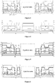
Figure 1 is a schematic structural view of a display panel in the present application. -
Figure 2 is a schematic structural view of a display panel without an aperture area of the present application. -
Figure 3 is a schematic structural view of a display panel inFigure 2 with an aperture area . -
Figure 4 is a schematic structural view of a display panel without an aperture area of the present application. -
Figure 5 is a schematic structural view of a display panel inFigure 4 with an aperture area. -
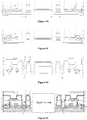
Figure 6 is a schematic structural view of a display panel with an aperture area of the present application. -
Figure 7 is a schematic structural view of a display panel with an aperture area of the present application. -
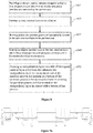
Figure 8 is a flowchart of a method for manufacturing a display panel of the present application. -
Figures 9a-9e are schematic structural views of a process for manufacturing a display panel of the present application. - At present, in order to achieve a full screen display, a mounting hole is generally disposed in the display area of the display device (such as a mobile phone), and functional components such as cameras, sensors, or earpieces are disposed in the mounting hole. However, there is a risk of encapsulation failure for arranging the mounting hole in the display area, which in turn affects the display effect of the display panel. After research, the applicant found that it is mainly because that after installing the mounting hole in the display area, an organic material layer on a side wall of the mounting hole is exposed, and the exposed part of the organic material layer is more likely to be invaded by water and oxygen, which makes a planarization layer, insulating layer, hole injection layer, hole transport layer, organic light emitting layer, electron transport layer, electron injection layer or cathode layer and other organic material layers form a channel for water and oxygen to enter the display area, thus causing encapsulation failure of the display area, and affects the display effect of the display panel.
- In view of the above technical problems, the present application provides a display panel and a method for preparing the same and a display device. The inventors has realized a partition of a water and oxygen entry channel by separating the organic material layer around the mounting hole, which can solve the above technical problem and prevent the encapsulation failure of the display area and ensure the display effect of the display panel.
- The present application provides a display panel. As shown in
Figure 1 , thedisplay panel 100 provided by the present application comprises adisplay area 101, anaperture area 102 located in thedisplay area 101, and apartition area 103 surrounding theaperture area 102, wherein theaperture area 102 is provided with a mounting hole therein, and the mounting hole is used to mount functional elements such as a camera, a sensor or an earpiece, so as to increase a screen ratio and improve visual enjoyment of the user. - Optionally, as shown in
Figure 2 or3 , thedisplay panel 100 comprises asubstrate 1 wherein thesubstrate 1 comprises adisplay area 101, anaperture area 102 located in thedisplay area 101, and apartition area 103 surrounding theaperture area 102; and thepartition area 103 is provided with at least onepartition ring 113, and apartition groove 123 is disposed on at least one side of thepartition ring 113, and the partition groove comprises athird partition groove 1233, afirst partition groove 1231, and a second partition groove 1232 that are disposed on a side away from the substrate and communicated with each other. As shown inFigure 3 , thethird partition grooves 1233, thefirst partition grooves 1231 and the second partition grooves 1232 are arranged in sequence on a surface of a side away from the substrate in sequence. Thethird partition groove 1233 is located near the substrate, thefirst partition groove 1231 is located on a side of thethird partition groove 1233 away from the substrate, and the second partition groove 1232 is located at an uppermost position of the side of thefirst partition groove 1231 away from thethird partition groove 1233. Thefirst partition groove 1231 is used to partition anorganic material layer 10 on the side wall of the second partition groove 1232 and thethird partition groove 1233; the material at a bottom of thefirst partition groove 1231 and the material covering the interior of thepartition groove 123, and the material of theencapsulation layer 11 in contact with the bottom of the third partition groove are of the same type. - Specifically, the
first partition groove 1231 is formed before the preparation of the pixel defining layer, that is, the pixel defining layer is prepared after the preparation of thefirst partition groove 1231, so that the pixel defining layer is filled at the bottom of thefirst partition groove 1231, and the pixel defining layer can't be removed through an exposure process, which may cause that the organic material layer cannot be partitioned in subsequent evaporation of the organic material layer, and lead to encapsulation failure of the display panel. Based on this fact, thepartition ring 113 can have a gourd shape, and a pixel defining layer is located at an upper layer of thepartition ring 113, which prevents thefirst partition groove 1231 from being filled with organic film layer such as the pixel defining layer, and thus effectively isolating the organic material layer and improving encapsulation effect. In addition, a crack dam can be omitted through the setting of the partition ring, and a frame area of the aperture area can be reduced, therefore the screen ratio can be further increased. - Optionally, the
substrate 1 comprises a first flexible layer, a first barrier layer, and a second flexible layer, and an array structure layer is formed on a side of the second flexible layer away from the first barrier layer. The first barrier layer arranged between the first flexible layer and the second flexible layer can improve the ability of the flexible substrate to block water and oxygen. Specifically, the first flexible layer and the second flexible layer comprises a material such as polyimide (PI), and the first flexible layer has a thickness of 8-12 µm, preferably 10 µm, and the second flexible layer has a thickness of 8-12µm, preferably 10µm. The first barrier layer is an inorganic layer, the inorganic layer comprises a material of silicon oxide (SiOx) or silicon nitride (SiNx) or other materials, and the first barrier layer has a thickness of 0.8-1.2µm, preferably 1µm. The setting of the thickness of the first barrier layer may not only optimize the effect of blocking external water or vapor, but also reduce a thickness of the display panel to achieve lightness and thinness. - In the above display panel, a
partition groove 123 or apartition ring 113 is provided to partition theorganic material layer 10,the material at the bottom of thefirst partition groove 1231, the material covering the interior of thepartition groove 123, and the material of the encapsulation layer in contact with the bottom of the groove are of the same type, on the one hand, the organic light-emitting layer is partitioned to block water and oxygen from the entry channel, and improve the encapsulation effect of the display panel; on the other hand, an adhesion force of the film layer can be improved, so that the inorganic film layer in theencapsulation layer 11 and the inorganic film layer at the bottom of thepartition groove 123 are closely bonded to further enhance an encapsulation effect and prevent external water and oxygen from entering the organic material layer in thedisplay area 101 via theaperture area 102, and improve a encapsulation effect, service life and display effect of the display panel. - Optionally, in the display panel of the embodiment of the present application, the
third partition groove 1233, thefirst partition groove 1231, and the second partition groove 1232 are arranged in sequence along a stacking direction that forms a certain angle with the display panel (for example, 75°, 80°, 90°, etc.). - Optionally, as shown in
Figure 3 , in the embodiment of the present application, the example is described when thethird partition groove 1233, thefirst partition groove 1231, and the second partition groove 1232 are arranged along the stacking direction orthogonal to the display panel, which is not used to limit the present application. - In the stacking direction orthogonal to the display panel, a diameter W2 of the groove opening on a side of the
first partition groove 1231 away from thesubstrate 1 is larger than a diameter W1 of the groove opening on a side of the second partition groove 1232 near thesubstrate 1, a diameter of the groove opening on a side of thefirst partition groove 1231 near the substrate is larger than a diameter of the groove opening on a side of thethird partition groove 1233 away from the substrate ; so that theorganic material layer 10 is partitioned at thefirst partition groove 1231. - Optionally, as shown in
Figure 3 or Figure 6 , in the stacking direction orthogonal to the display panel, thefirst partition groove 1231 has an inverted trapezoid shape or hexagon shape in cross section; each side wall of thefirst partition groove 1231, the second partition groove 1232 and thethird partition grooves 1233 forms an angle larger than 90° with respective bottom plane to which the side wall corresponds. Specifically, when the partition groove is cut along an axis of thepartition groove 123, in the cross section of the cut groove, a side wall of the section forms an angle larger than 90° with the bottom wall of the section. This structure arrangement is beneficial for forming a tightly adhered film on the side wall of thepartition groove 123 when the inorganic layer of theencapsulation layer 11 is formed by a chemical vapor deposition (CVD) process, thereby improving the encapsulation effect. - Optionally, the
partition groove 123 is an annular groove. The annular partition groove is arranged around theaperture area 102 to partition the organic material layer between theaperture area 102 and thedisplay area 101, thereby partitioning the channel of water and oxygen entering the display area, and improving the service life and display effect of the display panel. - As shown in
Figures 2-7 , theaperture area 102 is provided with a mounting hole passing through thedisplay panel 100 for mounting functional elements, apartition groove 123 is arranged around the mounting hole, and apartition ring 113 is disposed between thepartition groove 123 and the mounting hole to partition theorganic material layer 10; specifically, the functional element may be a camera, a sensor, a microphone, an earpiece, or a physical button, etc. - Optionally, at least two partition rings 113 are arranged around the mounting hole. The
partition ring 113 is a ring-shaped partition ring arranged around the mounting hole to partition theorganic material layer 10. By providing a plurality of partition rings, theorganic material layer 10 can be better and more thoroughly partitioned to improve the encapsulation effect of the display panel. - Further, the
display panel 100 further comprises an array structure layer disposed on thesubstrate 1, and at least part of thepartition grooves 123 are disposed in the array structure layer. - Optionally, a buffer layer is arranged between the
substrate 1 and the array structure layer, at least part of thepartition groove 123 passes through the buffer layer, and the material of the encapsulation layer in contact with the groove bottom of thepartition groove 123 is the same type as the material of the buffer layer; that is, the material of the buffer layer exposed at the bottom of thepartition groove 123 is the same type as the material of a side of theencapsulation layer 11 near thesubstrate 1. For example, both of the material can be inorganic material including silicon nitride or silicon oxide. Such setting can not only partition the organic material layer, but also improve an adhesion force of the film layer, so that the inorganic film layer in theencapsulation layer 11 and the inorganic film layer of the buffer layer are closely bonded, which can enhance the encapsulation effect and prevent external water and oxygen from entering theorganic material layer 10 in thedisplay area 101 via theaperture area 102, and improve the encapsulation effect, service life and display effect of the display panel. - Further, as shown in
Figure 3 , the buffer layer comprises a firstinorganic layer 2 adjacent to thesubstrate 1 and a secondinorganic layer 3 away from thesubstrate 1. Thepartition groove 123 passes through the secondinorganic layer 3. The material ofencapsulation layer 11 in contact with the bottom of thepartition groove 123 is the same type as the material of the firstinorganic layer 2; specifically, the material of the firstinorganic layer 2 comprises silicon nitride (SiNx), and the material of the secondinorganic layer 3 comprises silicon oxide (SiOx), by setting such two inorganic buffer layers, it can not only improve the encapsulation effect, but also contribute to heat insulation. At the same time, by setting such silicon nitride (SiNx) layer, pollutants from the glass substrate, especially sodium ions, can be blocked, and leakage current caused by the pollutants can be avoided. In addition, by setting a silicon oxide (SiOx) layer, a heat conduction loss in the excimer laser anneal (ELA) process can be avoided, which is beneficial to the formation of large crystal grains and reduces the interface defects of polysilicon. - Optionally, the
encapsulation layer 11 is a thin-film encapsulation layer. The thin-film encapsulation layer comprises a third inorganic layer, an organic layer, and a fourth inorganic layer stacked in sequence. The fourth inorganic layer is near theorganic material layer 10 and overlies theorganic material layer 10. The material of the fourth inorganic layer and the material of the bottom of thepartition groove 123 are of the same type; the third inorganic layer has a thickness of 0.8-1.2µm, such as 1µm, the organic layer has a thickness of 8-12µm, such as 10µm, the fourth inorganic layer has a thickness of 0.8-1.2 µm, such as 1 µm. - Preferably, the first inorganic layer, the second inorganic layer, the third inorganic layer and the fourth inorganic layer are all made of silicon oxide or silicon nitride. The inorganic layers can be used to improve the encapsulation effect while improving the adhesion force of the film layer.
- Optionally, the
organic material layer 10 comprises a hole injection layer, a hole transport layer, an organic light-emitting layer, an electron transport layer, and an electron injection layer that are stacked, and the hole injection layer is disposed on the array structure layer. - Optionally, as shown in
Figure 3 , the array structure layer comprises a pixel circuit layer, a planarization layer, and a pixel defining layer. The pixel circuit layer forms respective film layers of a thin film transistor, such as a semiconductor layer (P-Si) formed on the secondinorganic layer 3 of the buffer layer, agate insulating layer 4 formed on the semiconductor layer, acapacitor insulating layer 5 located above thegate insulating layer 4, an interlayer dielectric layer 6 located above thecapacitor insulating layer 5, and aplanarization layer 8 located above the interlayer dielectric layer 6, and apixel defining layer 9 located on theplanarization layer 8. The pixel circuit layer comprises the source (S), drain (D) and gate (M1) in the thin film transistor (Thin Film Transistor, TFT), the gate (M1) is located between thegate insulating layer 4 and thecapacitor insulating layer 5, the source (S) and drain (D) are in contact with the semiconductor layer (P-Si). A capacitor of the pixel circuit layer comprises a first plate (M1) and a second plate (M2). The first plate (M1) is located between the capacitor insulatinglayer 5 and the interlayer dielectric layer 6, and the second plate (M2) is located between thegate insulating layer 4 and thecapacitor insulating layer 5. - The display panel further comprises a first electrode and a second electrode. The first electrode is an anode. The first electrode comprises material such as silver-doped indium tin oxide, or silver-doped indium zinc oxide, or indium zinc oxide or indium tin oxide. The first electrode uses silver-doped indium tin oxide or silver-doped indium zinc oxide to reduce a resistance of the first electrode. Optionally, the first electrode is a composite film layer of indium tin oxide and silver. For example, the first electrode comprises a three-layer composite film layer of indium tin oxide, silver and indium tin oxide; and the middle layer is configured as a silver layer, which can increase the conductivity of the first electrode. The second electrode is a cathode, and the second electrode is made of magnesium or silver.
- The present application also provides a display device including any of the above-mentioned display panels. For example, the display device can be a mobile phone, a television, a tablet, a computer, or a camera.
- The present application also provides a method for manufacturing a display panel, as shown in
Figures 9a-9e , including the following steps: - S10 providing a substrate comprising a display area, an aperture area located in the display area, and a partition area surrounding the aperture area;
- S20 forming an array structure layer on the substrate;
- S30 in the partition area, forming at least one partition groove at least partially located in the array structure layer;
- S40 forming an organic material layer on the array structure layer and in the partition groove, and the organic material layer is disconnected at the partition groove;
- S50 forming an encapsulation layer on a side of the organic material layer away from the substrate, the encapsulation layer covers an inner wall of the partition groove, the material at a bottom of the partition groove is the same as the material covering the partition groove, and the material of the encapsulation layer in contact with a bottom of the groove.
- The display panel prepared by the above preparation method, on the one hand, a partition groove and a partition ring can be formed between the aperture area and the display area to realize a partition of the organic light-emitting layer between the aperture area and the display area, thereby blocking water and oxygen from entering and improve the encapsulation layer; on the other hand, the material at a bottom of the partition groove is the same type as the material covering the interior of the partition groove, and the material of the encapsulation layer in contact with a bottom of the groove, for example, the material at the bottom of the partition groove is an inorganic material, and the material covering the interior of the partition groove and the material of the encapsulation layer in contact with the bottom of the groove are also an inorganic material, and the two materials are of the same type such as silicon nitride (SiNx) or silicon oxide (SiOx), which can improve an adhesion force of the film layer, make the bottom of the groove and the encapsulation layer more tightly bonded, and further improve the encapsulation effect, and the inorganic material can effectively block water and oxygen, and ensure service life and display effect of the display panel.
- As explained in the above technical solution, the inventor found that when preparing the mounting hole in the display area, the reason why the organic material layer in the aperture area cannot be effectively disconnected is mainly because the organic material layer such as the pixel defining layer can be filled in the first partition groove during the preparation process, which is difficult to be removed through an exposure process. During subsequent evaporation of the organic material layer, the organic material layer cannot be partitioned, which affects the actual encapsulation effect and display effect of the display panel. Therefore, the inventors firstly stacked an array structure layer on the substrate, and then formed a partition groove passing through the array structure layer. In a direction orthogonal to the stacking direction of the display panel, the partition groove comprises a
third partition groove 1233, thefirst partition groove 1231 and the second partition groove 1232, which are located on the side away from a surface of the substrate and communicated with each other. Specifically, thethird partition groove 1233, thefirst partition groove 1231, and the second partition groove 1232 are arranged in sequence along a surface away from the substrate. Thethird partition groove 1233 is arranged near the substrate. Thepartition groove 1231 is located at a side of thethird partition groove 1233 away from the substrate, and the second partition groove 1232 is located at a side of thefirst partition groove 1231 away from thethird partition groove 1233, and arranged at an uppermost position. A diameter of the groove opening on the side of thefirst partition groove 1231 away from the substrate is larger than a diameter of the groove opening on the side of the second partition groove near the substrate, that is, a groove wall of thefirst partition groove 1231 is recessed inward to make the organic material layer partitioned at thefirst partition groove 1231. Optionally, thefirst partition groove 1231 in the present application is formed after forming the pixel defining layer , which can prevent the pixel defining layer from entering thefirst partition groove 1231, therefore, when the mounting hole is prepared, the organic material layer in the aperture area is disconnected, which can prevent water and oxygen from entering the display area via the aperture area, and improve the encapsulation effect, service life and display effect of the display panel. - Further, the step of forming at least one partition groove at least partially located in the array structure layer in the partition area comprises:
A hole is punched in the array structure layer located in the partition area to form at least one first partition hole, and the first partition hole is filled with a metal material to form a metalsacrificial layer 13; aplanarization layer 8 is formed on the array structure layer. As shown inFigures 9a and9b , theplanarization layer 8 and part of the metalsacrificial layer 13 are etched to expose part of the metalsacrificial layer 13 to form a second partition hole. Further, as shown inFigure 9c , in the second partition hole, the remaining material of the metalsacrificial layer 13 is removed to form apartition groove 123 for partitioning theorganic material layer 10, so that theorganic material layer 10 is disconnected at a position where the metalsacrificial layer 13 is removed. The preparation of thepartition groove 123 can be achieved through the above process, which can simplify the process and reduce the effects on the display panel. - Optionally, removing the remaining metal
sacrificial layer 13 to form thepartition groove 123 can be achieved by a wet etching process. Other film layers will not be affected while removing the remaining metal sacrificial layer, which ensures reliability of the display panel. - Further, in the stacking direction orthogonal to the
display panel 100, thepartition groove 123 comprises afirst partition groove 1231 near thesubstrate 1 and a second partition groove 1232 away from thesubstrate 1. A diameter W2 of the groove opening on one side of thefirst partition groove 1231 away from thesubstrate 1 is larger than the diameter W1 of the groove opening on the side of the second partition groove 1232 near thesubstrate 1, that is, a diameter difference is formed between thefirst partition groove 1231 and the second partition groove 1232, so that the organic material layer is partitioned at thefirst partition groove 1231. - Optionally, as shown in
Figure 9d , along the stacking direction from the substrate to the encapsulation layer, thefirst partition groove 1231 has an inverted trapezoid shape in cross section. The angle between a sidewall of thefirst partition groove 1231 and the bottom of the partition groove can be larger than 90°, so that the encapsulation layer can be in close contact with the groove wall of the partition groove, which increases the adhesion force of the film layer and improves the encapsulation effect. - Optionally, before forming the second partition hole, the method further comprises:
Apixel defining layer 9 is formed on theplanarization layer 8 located in the partition area; thepixel defining layer 9 and theplanarization layer 8 and part of the metalsacrificial layer 13 are etched to expose part of the metalsacrificial layer 13 to form a second partition hole, which can be used to avoid that the organic material layer can't be effectively partitioned as the material of the pixel defining layer is deposited in the partition groove. - Optionally, a
partition ring 113 is formed betweenadjacent partition grooves 123 to partition theorganic material layer 10. - Preferably, the metal sacrificial layer comprises a material such as titanium and/or aluminum.
- Optionally, the metal sacrificial layer can be formed by a separate process, or can be formed in the same process step with the metal layer of the array structure layer. The metal layer in the array structure layer may comprise an electrode layer (a first electrode or a second electrode in a capacitor, or the gate electrode, etc.) or a wiring layer (data line or scan line).
- Optionally, the step of forming at least one partition groove at least partially located in the array located in the structure layer of the partition area comprises the following:
A hole is punched in the array structure layer located in the partition area to form at least one first partition hole, and the first partition hole is filled with a metal material to form a metalsacrificial layer 13; aplanarization layer 8 is formed on the array structure layer; the material of theplanarization layer 8 and part of the metalsacrificial layer 13 are etched to expose part of the metalsacrificial layer 13 to form a second partition hole; part of the metalsacrificial layer 13 is removed to form apartition groove 123 for partitioning the organic material layer. - Through the process, the partition groove can also be formed to achieve the partition of the organic material layer and improve the encapsulation effect; at the same time, the material of part of the metal sacrificial layer is removed to form a partition groove. As shown in
Figure 6 or7 , in a stacking direction orthogonal to thedisplay panel 100, thepartition groove 123 comprises afirst partition groove 1231 near thesubstrate 1 and a second partition groove 1232 away from thesubstrate 1; a maximum diameter of thefirst partition groove 1231 is larger than a diameter of the groove opening on the side of the second partition groove 1232 near thesubstrate 1, so that theorganic material layer 10 is partitioned at thefirst partition groove 1231. - Specifically, along the stacking direction of the
substrate 1 to theencapsulation layer 11, thefirst partition groove 1231 has a hexagon shape in cross section, and the side wall of thepartition groove 123 connected to the bottom of thepartition groove 123 forms an angle larger than 90° with a bottom-located plane of thepartition groove 123. At this time, the metal sacrificial layer comprises a three-layer structure, for example, the three-layer structure comprise materials of titanium/aluminum/titanium (Ti/Al/Ti), through selecting different etching rate, an etching rate of the aluminum metal layer is larger than that of the titanium metal layer, so that thefirst partition groove 1231 has a hexagonal shape in cross section, and a sidewall of thepartition groove 123 connected to the bottom of thepartition groove 123 forms an angle larger than 90° with a bottom-located plane of thepartition groove 123, which can effectively improve the encapsulation effect and prevent the intrusion of water and oxygen. - Optionally, before forming the second partition hole, the method further comprises the following:
Apixel defining layer 9 is formed on theplanarization layer 8 located in the partition area; thepixel defining layer 9 and theplanarization layer 8 and part of the metalsacrificial layer 13 are etched to expose part of the metalsacrificial layer 13 to form a second partition hole, which can be used to avoid that the organic material layer can't be effectively partitioned as the material of the pixel defining layer is deposited in the partition groove. - Further, a
partition ring 113 is formed betweenadjacent partition grooves 123 to partition theorganic material layer 10, which can also have the effect of blocking cracks. - Optionally, the metal
sacrificial layer 13 comprises materials of titanium and/or aluminum. Preferably, the first partition groove is filled with titanium, aluminum and titanium in sequence to form a metal sacrificial layer with a three-layer structure comprising a titanium layer, an aluminum layer and a titanium layer. - Further, the metal sacrificial layer and a metal lead layer of the array structure layer are formed in the same process step. The metal leads include scan lines and data lines.
- Further, as shown in
Figure 2 , the method further comprises the following:
A buffer layer is formed on the substrate, and at least a part of thepartition groove 123 passes through the buffer layer. - Preferably, the buffer layer comprises a first
inorganic layer 2 near thesubstrate 1 and a secondinorganic layer 3 away from thesubstrate 1. Thepartition groove 123 passes through the secondinorganic layer 3; that is, the firstinorganic layer 2 is exposed at a bottom of the partition groove and theencapsulation layer 11 is in direct contact with the firstinorganic layer 2, which can improve the film adhesion force. - Preferably, the method for manufacturing the
display panel 100 further comprises: as shown inFigure 9e , after theencapsulation layer 11 is prepared, a mounting hole passing through the display panel is arranged in theaperture area 102 of thedisplay panel 100 for mounting functional components, such as a camera, or earpiece, etc. - As shown in
Figure 3 , the array structure layer comprises a semiconductor layer (P-Si) on the secondinorganic layer 3 of the buffer layer, agate insulating layer 4 on the semiconductor layer, acapacitor insulating layer 5 on thegate insulating layer 4, an interlayer dielectric layer 6 on thecapacitor insulating layer 5, aplanarization layer 8 on the interlayer dielectric layer 6, and apixel defining layer 9 on theplanarization layer 8 that are stacked. The pixel circuit layer comprises a source (S), drain (D) and gate (M1) in the thin film transistor (Thin Film Transistor, TFT). - The gate (M1) is located between the
gate insulating layer 4 and thecapacitor insulating layer 5, the source (S) and drain (D) are in contact with the semiconductor layer (P-Si) layer. The capacitor of the pixel circuit layer comprises a first plate (M1) and a second plate (M2). The first plate (M1) is located between the capacitor insulatinglayer 5 and the interlayer dielectric layer 6, and the second plate (M2) is located between thegate insulating layer 4 and thecapacitor insulating layer 5. The semiconductor layer is made of P-Si or α-Si, and has a thickness of 45-55nm; thegate insulating layer 4 has a thickness of 95-105nm, and is made of silicon oxide or zirconium oxide; the gate (M1) has a thickness of 245-255 nm, and thecapacitor insulating layer 5 has a thickness of 95-105 nm. The pixel circuit is used to drive the organic light emitting device to emit light. - An
anode 12 is formed on theplanarization layer 8, apixel defining layer 9 is formed on theplanarizing layer 8 and theanode 12 located in the display area, and thepixel defining layer 9 is etched to expose at least part of theanode 12 to form a pixel opening, in which an organic material layer is prepared and a cathode is formed on the organic material layer. Optionally, thepixel defining layer 9 may be or may not be formed on the planarization layer located in the partition area; the display panel also comprises a spacer (SPC) arranged on thepixel defining layer 9 with a height of 1400-1600 nm, preferably 1500 nm, and used to support a mask when the organic light-emitting material is evaporated. - In the display panel and the a method for preparing the same and the display device provided in the present application, the display panel has a mounting hole for mounting functional elements such as a camera, a partition ring and a partition groove are arranged around the mounting hole, and the partition of the organic material layer between the aperture area and display area can be achieved through the partition ring and the partition groove, so as to prevent water and oxygen from entering the display area of the display panel, and improves the service life and display effect of the display panel. In addition, the setting of the partition groove can also function to prevent cracks.
Claims (20)
- A display panel, comprising a substrate, wherein the substrate comprises:a display area,an aperture area, located in the display area; anda partition area, surrounding the aperture area and provided with at least one partition ring disposed around the aperture area, wherein a partition groove is disposed on at least one side of the partition ring,which characterized in that the partition groove comprises a third partition groove, a first partition groove, and a second partition groove that are disposed on a side away from the substrate in sequence and communicated with each other, andthe first partition groove is used to separate an organic material layer on a side wall of the second partition groove from another organic material layer on a side of the third partition groove.
- The display panel of claim 1, wherein,the third partition groove, the first partition groove, and the second partition groove are disposed along a side away from the surface of the substrate in a direction orthogonal to a stacking direction of the display panel, anda diameter of a groove opening on the side of the first partition groove away from the substrate is larger than a diameter of a groove opening on the side of the second partition groove near the substrate, anda diameter of a groove opening on the side of the first partition groove near the substrate is larger than a diameter of a groove opening on the side of the third partition groove away from the substrate.
- The display panel of claim 1, wherein,the first partition groove has an inverted trapezoid shape or a hexagon in cross section in a direction orthogonal to the stacking direction of the display panel; andan angle between a side wall and a bottom-located plane of each of the first partition groove, the second partition groove and the third partition groove is larger than 90°.
- The display panel according to claim 1, wherein,a mounting hole through the display panel is disposed in the aperture area, and used for mounting functional elements, andthe partition groove is arranged around the mounting hole, and the partition ring is arranged between the partition groove and the mounting hole to partition the organic material layer.
- The display panel of claim 4, wherein
at least two partition rings are disposed around the mounting hole to partition the organic material layer . - The display panel according to any one of claims 1 to 5, wherein,
the display panel further comprises an array structure layer disposed on the substrate, and the partition groove is at least partially disposed inside the array structure layer. - The display panel of claim 6, wherein,a buffer layer is provided between the substrate and the array structure layer, and the partition groove at least partially passes through the buffer layer, andan encapsulation layer which is in contact with a bottom of the partition groove comprises a material the same as that of the buffer layer.
- The display panel of claim 7, wherein,the buffer layer comprises a first inorganic layer adjacent to the substrate,a second inorganic layeris disposed away from the substrate, and the partition groove extends through the second inorganic layer, andthe encapsulation layer which is in contact with a bottom of the partition groove comprises a material the same as that of the first inorganic layer .
- The display panel according to claim 8, wherein,the encapsulation layer is a thin-film encapsulation layer and comprises a third inorganic layer, an organic layer, and a fourth inorganic layer stacked in sequence, andthe fourth inorganic layer is close to the organic material layer and overlies the organic material layer, and the fourth inorganic layer comprise a material same as that of the bottom of the partition groove.
- A display device, characterized by comprising the display panel according to any one of claims 1-9.
- A method for manufacturing a display panel , characterized by comprising the following steps:providing a substrate, comprising a display area, an aperture area located in the display area, and a partition area surrounding the aperture area;forming an array structure layer on the substrate, presetting at least two metal sacrificial layers spaced apart along a direction parallel to the substrate in the partition area, and forming a second partition hole between adjacent metal sacrificial layers , so that the metal sacrificial layer is exposed on a side wall of the second partition hole;removing the metal sacrificial layer to form at least one partition groove at least partially in the array structure layer;forming an organic material layer on the array structure layer and in the partition groove, and the organic material layer is disconnected at a location where the metal sacrificial layer is removed.
- The method of claim 11, wherein,
the metal sacrificial layer is formed by the step of:punching a hole in the array structure layer located in the partition area to form at least one first partition hole, which is filled with a metal material to form the metal sacrificial layer. - The method of claim 12, wherein,
the step of exposing the metal sacrificial layer comprises:forming a planarization layer on the array structure layer;etching materials of the planarization layer and part of the metal sacrificial layer to expose part of the metal sacrificial layer to form a second partition hole. - The method according to claim 13, before forming the second partition hole, further comprising:forming a pixel defining layer on the planarization layer located in the partition area;etching the pixel defining layer, the planarization layer, and part of the metal sacrificial layer material to expose part of the metal sacrificial layer to form a second partition hole.
- The method according to claim 11, wherein,
a partition ring is formed between adjacent partition grooves. - The method according to claim 11, wherein,
the metal sacrificial layer comprises materials of titanium and/or aluminum. - The method of claim 12, wherein,
the metal sacrificial layer and a metal wiring layer of the array structure layer are formed in the same process step. - The method according to any one of claims 11-18, further comprising:forming a buffer layer on the substrate, and at least part of the partition groove passing through the buffer layer.
- The method according to claim 18, wherein,the buffer layer comprises a first inorganic layer adjacent to the substrate and a second inorganic layer away from the substrate, andthe partition groove passes through the second inorganic layer.
- The method of claim 18, further comprising, after preparing the encapsulation layer, opening a mounting hole passing through the display panel in the aperture area of the display panel for mounting functional components.
Applications Claiming Priority (3)
| Application Number | Priority Date | Filing Date | Title |
|---|---|---|---|
| CN201910703770.5A CN110429118A (en) | 2019-07-31 | 2019-07-31 | Display panel, manufacturing method thereof, and display device |
| CN201911120612.3A CN110828519B (en) | 2019-07-31 | 2019-11-15 | Display panel, preparation method thereof and display device |
| PCT/CN2020/081524 WO2021017501A1 (en) | 2019-07-31 | 2020-03-27 | Display panel, preparation method therefor and display apparatus |
Publications (3)
| Publication Number | Publication Date |
|---|---|
| EP3923337A1 true EP3923337A1 (en) | 2021-12-15 |
| EP3923337A4 EP3923337A4 (en) | 2022-06-08 |
| EP3923337B1 EP3923337B1 (en) | 2023-07-12 |
Family
ID=68413485
Family Applications (1)
| Application Number | Title | Priority Date | Filing Date |
|---|---|---|---|
| EP20847081.5A Active EP3923337B1 (en) | 2019-07-31 | 2020-03-27 | Display panel, preparation method therefor and display apparatus |
Country Status (7)
| Country | Link |
|---|---|
| US (1) | US12185566B2 (en) |
| EP (1) | EP3923337B1 (en) |
| JP (1) | JP7194291B2 (en) |
| KR (1) | KR102674697B1 (en) |
| CN (2) | CN110429118A (en) |
| TW (1) | TWI722856B (en) |
| WO (1) | WO2021017501A1 (en) |
Families Citing this family (63)
| Publication number | Priority date | Publication date | Assignee | Title |
|---|---|---|---|---|
| CN109560114B (en) * | 2018-12-06 | 2021-01-26 | 京东方科技集团股份有限公司 | Display panel manufacturing method, display panel and display device |
| KR102168042B1 (en) | 2018-12-27 | 2020-10-20 | 엘지디스플레이 주식회사 | Display Device |
| CN110429118A (en) * | 2019-07-31 | 2019-11-08 | 云谷(固安)科技有限公司 | Display panel, manufacturing method thereof, and display device |
| CN110854304B (en) * | 2019-11-20 | 2021-03-26 | 云谷(固安)科技有限公司 | Manufacturing method of display panel |
| CN110890474B (en) * | 2019-11-27 | 2022-04-26 | 武汉天马微电子有限公司 | Display panel and display device |
| CN110911421B (en) * | 2019-11-29 | 2023-04-07 | 京东方科技集团股份有限公司 | Back plate for organic light-emitting display panel, manufacturing method and display panel |
| CN110993660B (en) * | 2019-11-29 | 2022-10-11 | 武汉天马微电子有限公司 | Display panel and display device |
| CN113632234B (en) | 2019-12-11 | 2024-09-03 | 京东方科技集团股份有限公司 | Display substrate and manufacturing method thereof, and display device |
| CN111063713B (en) * | 2019-12-12 | 2022-03-29 | 武汉华星光电半导体显示技术有限公司 | OLED display panel, preparation method thereof and terminal device thereof |
| CN113013177B (en) * | 2019-12-20 | 2024-05-07 | 京东方科技集团股份有限公司 | Display panel and manufacturing method thereof, and display device |
| KR102778476B1 (en) * | 2020-01-02 | 2025-03-12 | 삼성디스플레이 주식회사 | Display device |
| CN111180465B (en) * | 2020-01-03 | 2022-09-23 | 京东方科技集团股份有限公司 | Display panel, preparation method and display device |
| CN111192974B (en) * | 2020-01-07 | 2022-07-12 | 武汉华星光电半导体显示技术有限公司 | Array substrate and preparation method thereof |
| CN111244140B (en) * | 2020-01-15 | 2023-04-25 | 云谷(固安)科技有限公司 | Method for manufacturing display panel and display panel |
| CN111403627B (en) * | 2020-03-26 | 2022-05-03 | 武汉华星光电半导体显示技术有限公司 | Display panel, manufacturing method thereof and display device |
| WO2021203351A1 (en) * | 2020-04-09 | 2021-10-14 | 京东方科技集团股份有限公司 | Display panel and manufacturing method thereof, hole formation precision measurement method, and display device |
| CN111490182B (en) * | 2020-04-24 | 2023-01-31 | 京东方科技集团股份有限公司 | Display back plate, manufacturing method thereof and display device |
| CN114127945B (en) * | 2020-04-29 | 2023-07-14 | 京东方科技集团股份有限公司 | Organic light-emitting display substrate, manufacturing method thereof, and organic light-emitting display device |
| CN111415974B (en) * | 2020-04-29 | 2022-10-04 | 武汉华星光电半导体显示技术有限公司 | OLED display panel and preparation method thereof |
| CN114127946B (en) * | 2020-04-29 | 2022-10-11 | 京东方科技集团股份有限公司 | Organic light-emitting display substrate, manufacturing method thereof and organic light-emitting display device |
| KR102845809B1 (en) | 2020-04-29 | 2025-08-13 | 삼성디스플레이 주식회사 | Display panel and display apparatus including the same |
| CN114144886B (en) * | 2020-05-15 | 2023-01-31 | 京东方科技集团股份有限公司 | Display substrate, manufacturing method thereof, and display device |
| CN111564478B (en) * | 2020-05-19 | 2022-11-04 | 京东方科技集团股份有限公司 | Stretchable display substrate, preparation method thereof, and display device |
| CN111725267A (en) * | 2020-06-02 | 2020-09-29 | 武汉华星光电半导体显示技术有限公司 | Display panel, preparation method thereof and display device |
| CN111725421B (en) * | 2020-06-09 | 2023-02-03 | 武汉华星光电半导体显示技术有限公司 | Organic light emitting diode display panel and display device |
| CN111725423A (en) * | 2020-06-10 | 2020-09-29 | 武汉华星光电半导体显示技术有限公司 | OLED device, preparation method thereof and display device |
| CN111653522B (en) * | 2020-06-16 | 2023-11-28 | 京东方科技集团股份有限公司 | A method for manufacturing a display substrate, a display substrate and a display device |
| CN113921733B (en) * | 2020-07-10 | 2025-05-27 | 华为技术有限公司 | Display panel, flexible display screen, electronic device and method for preparing display panel |
| WO2022018846A1 (en) * | 2020-07-22 | 2022-01-27 | シャープ株式会社 | Display device |
| CN112018264B (en) | 2020-09-01 | 2023-04-28 | 合肥鑫晟光电科技有限公司 | Light-emitting substrate and preparation method thereof |
| US20230413615A1 (en) * | 2020-09-23 | 2023-12-21 | Sharp Kabushiki Kaisha | Display device |
| CN114284296A (en) * | 2020-09-27 | 2022-04-05 | 华为技术有限公司 | Display panel, flexible display screen, electronic equipment and preparation method of display panel |
| CN112151697B (en) * | 2020-09-28 | 2023-06-06 | 京东方科技集团股份有限公司 | Method for making display backplane, display backplane and display device |
| JP7442419B2 (en) * | 2020-10-29 | 2024-03-04 | 東京エレクトロン株式会社 | Manufacturing method of organic EL panel |
| CN112397675B (en) * | 2020-11-18 | 2022-07-22 | 合肥维信诺科技有限公司 | Display panel preparation method and display panel |
| CN112531003B (en) | 2020-12-01 | 2023-04-25 | 武汉天马微电子有限公司 | Display panel, preparation method of display panel and display device |
| CN112582573B (en) * | 2020-12-11 | 2022-11-01 | 合肥维信诺科技有限公司 | Display panel, preparation method thereof and display device |
| CN112599700B (en) * | 2020-12-14 | 2022-05-24 | 合肥维信诺科技有限公司 | Display substrate, display substrate preparation method and display device |
| KR102959776B1 (en) * | 2020-12-17 | 2026-04-30 | 삼성디스플레이 주식회사 | Display panel and electronic device including the same |
| US12127439B2 (en) * | 2020-12-23 | 2024-10-22 | Chengdu Boe Optoelectronics Technology Co., Ltd. | Display substrate and preparation method thereof, and display apparatus |
| CN112736093B (en) * | 2020-12-30 | 2022-10-04 | 武汉华星光电半导体显示技术有限公司 | Display panel and display device |
| CN112786804B (en) * | 2021-01-08 | 2022-07-12 | 武汉华星光电半导体显示技术有限公司 | Display panel and manufacturing method thereof |
| CN112802979A (en) * | 2021-01-11 | 2021-05-14 | 合肥维信诺科技有限公司 | Display panel and preparation method thereof |
| CN112802981A (en) * | 2021-01-14 | 2021-05-14 | 武汉华星光电半导体显示技术有限公司 | Display panel and display device |
| CN112820741B (en) * | 2021-01-18 | 2023-12-19 | 合肥维信诺科技有限公司 | Display substrate and display substrate preparation method |
| CN113013359B (en) * | 2021-02-24 | 2022-09-20 | 厦门天马微电子有限公司 | Display panel and display device |
| CN113053917B (en) * | 2021-03-10 | 2022-08-23 | 武汉华星光电半导体显示技术有限公司 | Display screen, array substrate and manufacturing method thereof |
| CN113555396B (en) * | 2021-07-08 | 2022-10-04 | 武汉华星光电半导体显示技术有限公司 | Display panel |
| CN116096187A (en) * | 2021-10-29 | 2023-05-09 | 北京小米移动软件有限公司 | Display panel and preparation method thereof |
| CN114203774B (en) * | 2021-11-18 | 2025-10-31 | 维信诺科技股份有限公司 | Display panel and preparation method thereof |
| CN114188493B (en) * | 2021-11-29 | 2025-01-10 | 惠州华星光电显示有限公司 | Display panel and display device |
| CN116209311B (en) * | 2021-11-30 | 2026-02-06 | 京东方科技集团股份有限公司 | Display substrate and display device |
| KR20230093112A (en) * | 2021-12-17 | 2023-06-27 | 삼성디스플레이 주식회사 | Display device |
| CN114464754B (en) | 2022-01-25 | 2023-05-12 | 武汉华星光电半导体显示技术有限公司 | Display panel and display device |
| CN114613923A (en) * | 2022-03-14 | 2022-06-10 | 武汉华星光电半导体显示技术有限公司 | Display panel and display device |
| CN114784060B (en) * | 2022-04-01 | 2025-12-05 | 深圳市华星光电半导体显示技术有限公司 | Display Panel and its Manufacturing Method |
| CN115050787A (en) * | 2022-06-10 | 2022-09-13 | 云谷(固安)科技有限公司 | Display panel, manufacturing method and display device |
| CN115020462A (en) * | 2022-06-21 | 2022-09-06 | 武汉华星光电半导体显示技术有限公司 | Array substrate, display panel and manufacturing method of array substrate |
| CN115207246B (en) * | 2022-07-14 | 2023-06-06 | 武汉华星光电半导体显示技术有限公司 | Display panel and display device |
| JP2025529602A (en) * | 2022-08-01 | 2025-09-05 | アプライド マテリアルズ インコーポレイテッド | Bezel-less camera and sensor hole |
| CN115411085B (en) * | 2022-09-20 | 2025-12-09 | 武汉天马微电子有限公司 | Display panel and display device |
| CN115547195B (en) * | 2022-09-21 | 2024-07-26 | 厦门天马显示科技有限公司 | Display panel, method for manufacturing display panel, and display device |
| CN117440714B (en) * | 2023-11-23 | 2024-11-08 | 惠科股份有限公司 | Display panel and display device |
Family Cites Families (34)
| Publication number | Priority date | Publication date | Assignee | Title |
|---|---|---|---|---|
| KR102028505B1 (en) * | 2012-11-19 | 2019-10-04 | 엘지디스플레이 주식회사 | Organic light-emtting diode display panel and method for fabricating the same |
| JP6114670B2 (en) * | 2013-09-19 | 2017-04-12 | 株式会社ジャパンディスプレイ | ORGANIC ELECTROLUMINESCENT DISPLAY DEVICE AND METHOD FOR PRODUCING ORGANIC ELECTROLUMINESCENT DISPLAY DEVICE |
| KR102395388B1 (en) * | 2014-12-02 | 2022-05-06 | 엘지디스플레이 주식회사 | Organic light emitting display device and method of manufacturing the same |
| KR102552272B1 (en) * | 2015-11-20 | 2023-07-07 | 삼성디스플레이 주식회사 | Organic light emitting display and manufacturing method using the same |
| US10205122B2 (en) | 2015-11-20 | 2019-02-12 | Samsung Display Co., Ltd. | Organic light-emitting display and method of manufacturing the same |
| KR102457252B1 (en) * | 2015-11-20 | 2022-10-24 | 삼성디스플레이 주식회사 | Organic light emitting display and manufacturing method using the same |
| KR102605208B1 (en) * | 2016-06-28 | 2023-11-24 | 삼성디스플레이 주식회사 | Organic light emitting display device and method of manufacturing an organic light emitting display device |
| KR102342609B1 (en) * | 2017-04-25 | 2021-12-22 | 후아웨이 테크놀러지 컴퍼니 리미티드 | Lcd display screen, electronic device, manufacturing method for lcd display screen |
| CN107331790A (en) * | 2017-07-19 | 2017-11-07 | 京东方科技集团股份有限公司 | A kind of OLED display panel and its method for packing, OLED display |
| CN107452894B (en) * | 2017-07-31 | 2020-02-18 | 京东方科技集团股份有限公司 | An organic electroluminescence display panel, its manufacturing method and display device |
| DE102017007479B4 (en) | 2017-08-08 | 2021-09-02 | Comet Ag | Objective and condenser for an X-ray tube, X-ray tube and a method for operating such an X-ray tube |
| KR102083646B1 (en) | 2017-08-11 | 2020-03-03 | 삼성디스플레이 주식회사 | Display panel and electronic device having the same |
| EP3441845B1 (en) * | 2017-08-11 | 2021-10-27 | Samsung Display Co., Ltd. | Display panel and electronic device having the same |
| KR102394984B1 (en) * | 2017-09-04 | 2022-05-06 | 삼성디스플레이 주식회사 | Display device and manufacturing method of the same |
| KR102374753B1 (en) * | 2017-09-04 | 2022-03-15 | 엘지디스플레이 주식회사 | Light Emitting Display Device and Manufacturing Method thereof |
| KR102083315B1 (en) * | 2017-09-11 | 2020-03-03 | 삼성디스플레이 주식회사 | Organic light-emitting display device and method of manufacturing the same |
| KR102448325B1 (en) * | 2017-11-16 | 2022-09-30 | 삼성디스플레이 주식회사 | Display panel and electronic device including same |
| KR102454390B1 (en) | 2017-12-05 | 2022-10-14 | 엘지디스플레이 주식회사 | Light Emitting Display Device |
| KR102014179B1 (en) * | 2017-12-08 | 2019-08-26 | 엘지디스플레이 주식회사 | Organic light emitting display device and method for manufacturing the same |
| KR102387343B1 (en) * | 2017-12-20 | 2022-04-15 | 엘지디스플레이 주식회사 | Display device |
| CN208094613U (en) * | 2018-03-09 | 2018-11-13 | 广东欧珀移动通信有限公司 | Electronic equipment |
| CN108666347B (en) | 2018-04-26 | 2021-07-30 | 上海天马微电子有限公司 | Display panel, method for manufacturing the same, and display device |
| CN109346617B (en) * | 2018-08-28 | 2020-08-25 | 信利半导体有限公司 | Full-color OLED display |
| CN109360843B (en) * | 2018-10-18 | 2022-10-28 | 京东方科技集团股份有限公司 | OLED display substrate, manufacturing method thereof and display device |
| CN109671870B (en) * | 2018-12-19 | 2021-05-07 | 武汉华星光电半导体显示技术有限公司 | Organic light emitting display device and method of manufacturing the same |
| CN109742264B (en) * | 2019-01-08 | 2020-07-31 | 京东方科技集团股份有限公司 | Display area opening packaging method, display area opening packaging structure and display panel |
| CN109786427A (en) | 2019-01-18 | 2019-05-21 | 京东方科技集团股份有限公司 | A kind of preparation method and display device of organic LED display device |
| CN109802052B (en) * | 2019-01-25 | 2021-05-07 | 上海天马微电子有限公司 | Organic light-emitting display panel and manufacturing method thereof |
| CN109742133B (en) * | 2019-02-28 | 2021-04-30 | 云谷(固安)科技有限公司 | Display panel, preparation method thereof and display device |
| CN109801956A (en) * | 2019-03-13 | 2019-05-24 | 京东方科技集团股份有限公司 | Display device, display panel and its manufacturing method |
| CN109873022B (en) | 2019-03-21 | 2021-01-22 | 京东方科技集团股份有限公司 | A kind of backplane, display device and preparation method of backplane |
| CN110224006B (en) * | 2019-05-13 | 2021-06-01 | 武汉华星光电半导体显示技术有限公司 | OLED display panel and preparation method thereof |
| US11043651B2 (en) | 2019-05-13 | 2021-06-22 | Wuhan China Star Optoelectronics Semiconductor Display Technology Co., Ltd. | OLED display panel and manufacturing method thereof |
| CN110429118A (en) * | 2019-07-31 | 2019-11-08 | 云谷(固安)科技有限公司 | Display panel, manufacturing method thereof, and display device |
-
2019
- 2019-07-31 CN CN201910703770.5A patent/CN110429118A/en active Pending
- 2019-11-15 CN CN201911120612.3A patent/CN110828519B/en active Active
-
2020
- 2020-03-27 KR KR1020217028635A patent/KR102674697B1/en active Active
- 2020-03-27 WO PCT/CN2020/081524 patent/WO2021017501A1/en not_active Ceased
- 2020-03-27 EP EP20847081.5A patent/EP3923337B1/en active Active
- 2020-03-27 JP JP2021552633A patent/JP7194291B2/en active Active
- 2020-04-01 TW TW109111339A patent/TWI722856B/en active
-
2021
- 2021-08-16 US US17/402,622 patent/US12185566B2/en active Active
Also Published As
| Publication number | Publication date |
|---|---|
| US20210376293A1 (en) | 2021-12-02 |
| WO2021017501A1 (en) | 2021-02-04 |
| EP3923337B1 (en) | 2023-07-12 |
| CN110828519B (en) | 2023-02-07 |
| EP3923337A4 (en) | 2022-06-08 |
| KR102674697B1 (en) | 2024-06-13 |
| CN110429118A (en) | 2019-11-08 |
| TW202030529A (en) | 2020-08-16 |
| US12185566B2 (en) | 2024-12-31 |
| JP2022523978A (en) | 2022-04-27 |
| CN110828519A (en) | 2020-02-21 |
| JP7194291B2 (en) | 2022-12-21 |
| KR20210123389A (en) | 2021-10-13 |
| TWI722856B (en) | 2021-03-21 |
Similar Documents
| Publication | Publication Date | Title |
|---|---|---|
| EP3923337B1 (en) | Display panel, preparation method therefor and display apparatus | |
| US12453276B2 (en) | Display panel | |
| JP7331016B2 (en) | DISPLAY SUBSTRATE AND MANUFACTURING METHOD THEREOF, DISPLAY DEVICE | |
| US12402490B2 (en) | Method for manufacturing an isolation area within a holing area and a display area of a display panel | |
| GB2610325A (en) | Display substrate and manufacturing method therefor, display panel, and display device | |
| CN112531003B (en) | Display panel, preparation method of display panel and display device | |
| CN110660930A (en) | Display panel, method for producing the same, and display device | |
| CN113851600A (en) | Display substrate, manufacturing method thereof and display device | |
| US11569472B2 (en) | Electroluminescent display substrate, manufacturing method thereof and electroluminescent display apparatus | |
| JP2023518622A (en) | DISPLAY SUBSTRATE AND MANUFACTURING METHOD THEREOF, DISPLAY MOTHERBOARD AND DISPLAY DEVICE | |
| WO2021012461A1 (en) | Array substrate, oled display panel, and display apparatus | |
| JP7485484B2 (en) | Display substrate, its manufacturing method, and display device | |
| WO2023088096A1 (en) | Display panel and manufacturing method therefor, and electronic device | |
| CN115084411A (en) | Display panel, display device and manufacturing method of display panel | |
| CN110660839A (en) | A display panel and its manufacturing method | |
| US12111554B2 (en) | Display substrate and display panel | |
| CN116867311A (en) | Display backplane, manufacturing method and display device | |
| CN219019442U (en) | Display device | |
| KR102866128B1 (en) | Display apparatus having a substrate hole | |
| CN120322111A (en) | Display panel, method for manufacturing display panel, and electronic device | |
| CN120201891A (en) | Display panel and display device | |
| CN118019387A (en) | Display panel, display device, and method for manufacturing display panel | |
| CN121419488A (en) | Display panel, display panel manufacturing method and electronic device |
Legal Events
| Date | Code | Title | Description |
|---|---|---|---|
| STAA | Information on the status of an ep patent application or granted ep patent |
Free format text: STATUS: THE INTERNATIONAL PUBLICATION HAS BEEN MADE |
|
| PUAI | Public reference made under article 153(3) epc to a published international application that has entered the european phase |
Free format text: ORIGINAL CODE: 0009012 |
|
| STAA | Information on the status of an ep patent application or granted ep patent |
Free format text: STATUS: REQUEST FOR EXAMINATION WAS MADE |
|
| 17P | Request for examination filed |
Effective date: 20210906 |
|
| AK | Designated contracting states |
Kind code of ref document: A1 Designated state(s): AL AT BE BG CH CY CZ DE DK EE ES FI FR GB GR HR HU IE IS IT LI LT LU LV MC MK MT NL NO PL PT RO RS SE SI SK SM TR |
|
| A4 | Supplementary search report drawn up and despatched |
Effective date: 20220506 |
|
| RIC1 | Information provided on ipc code assigned before grant |
Ipc: H01L 51/56 20060101ALI20220429BHEP Ipc: H01L 51/52 20060101ALI20220429BHEP Ipc: H01L 27/32 20060101AFI20220429BHEP |
|
| DAV | Request for validation of the european patent (deleted) | ||
| DAX | Request for extension of the european patent (deleted) | ||
| REG | Reference to a national code |
Ref country code: DE Free format text: PREVIOUS MAIN CLASS: H01L0027320000 Ipc: H10K0050844000 Ref country code: DE Ref legal event code: R079 Ref document number: 602020013870 Country of ref document: DE Free format text: PREVIOUS MAIN CLASS: H01L0027320000 Ipc: H10K0050844000 |
|
| GRAP | Despatch of communication of intention to grant a patent |
Free format text: ORIGINAL CODE: EPIDOSNIGR1 |
|
| STAA | Information on the status of an ep patent application or granted ep patent |
Free format text: STATUS: GRANT OF PATENT IS INTENDED |
|
| RIC1 | Information provided on ipc code assigned before grant |
Ipc: H10K 59/80 20230101ALI20230418BHEP Ipc: H10K 59/12 20230101ALI20230418BHEP Ipc: H10K 50/844 20230101AFI20230418BHEP |
|
| GRAS | Grant fee paid |
Free format text: ORIGINAL CODE: EPIDOSNIGR3 |
|
| GRAA | (expected) grant |
Free format text: ORIGINAL CODE: 0009210 |
|
| STAA | Information on the status of an ep patent application or granted ep patent |
Free format text: STATUS: THE PATENT HAS BEEN GRANTED |
|
| INTG | Intention to grant announced |
Effective date: 20230516 |
|
| AK | Designated contracting states |
Kind code of ref document: B1 Designated state(s): AL AT BE BG CH CY CZ DE DK EE ES FI FR GB GR HR HU IE IS IT LI LT LU LV MC MK MT NL NO PL PT RO RS SE SI SK SM TR |
|
| REG | Reference to a national code |
Ref country code: CH Ref legal event code: EP |
|
| REG | Reference to a national code |
Ref country code: DE Ref legal event code: R096 Ref document number: 602020013870 Country of ref document: DE |
|
| REG | Reference to a national code |
Ref country code: IE Ref legal event code: FG4D |
|
| REG | Reference to a national code |
Ref country code: LT Ref legal event code: MG9D |
|
| REG | Reference to a national code |
Ref country code: NL Ref legal event code: MP Effective date: 20230712 |
|
| REG | Reference to a national code |
Ref country code: AT Ref legal event code: MK05 Ref document number: 1588472 Country of ref document: AT Kind code of ref document: T Effective date: 20230712 |
|
| PG25 | Lapsed in a contracting state [announced via postgrant information from national office to epo] |
Ref country code: NL Free format text: LAPSE BECAUSE OF FAILURE TO SUBMIT A TRANSLATION OF THE DESCRIPTION OR TO PAY THE FEE WITHIN THE PRESCRIBED TIME-LIMIT Effective date: 20230712 |
|
| PG25 | Lapsed in a contracting state [announced via postgrant information from national office to epo] |
Ref country code: GR Free format text: LAPSE BECAUSE OF FAILURE TO SUBMIT A TRANSLATION OF THE DESCRIPTION OR TO PAY THE FEE WITHIN THE PRESCRIBED TIME-LIMIT Effective date: 20231013 |
|
| PG25 | Lapsed in a contracting state [announced via postgrant information from national office to epo] |
Ref country code: ES Free format text: LAPSE BECAUSE OF FAILURE TO SUBMIT A TRANSLATION OF THE DESCRIPTION OR TO PAY THE FEE WITHIN THE PRESCRIBED TIME-LIMIT Effective date: 20230712 |
|
| PG25 | Lapsed in a contracting state [announced via postgrant information from national office to epo] |
Ref country code: IS Free format text: LAPSE BECAUSE OF FAILURE TO SUBMIT A TRANSLATION OF THE DESCRIPTION OR TO PAY THE FEE WITHIN THE PRESCRIBED TIME-LIMIT Effective date: 20231112 |
|
| PG25 | Lapsed in a contracting state [announced via postgrant information from national office to epo] |
Ref country code: SE Free format text: LAPSE BECAUSE OF FAILURE TO SUBMIT A TRANSLATION OF THE DESCRIPTION OR TO PAY THE FEE WITHIN THE PRESCRIBED TIME-LIMIT Effective date: 20230712 Ref country code: RS Free format text: LAPSE BECAUSE OF FAILURE TO SUBMIT A TRANSLATION OF THE DESCRIPTION OR TO PAY THE FEE WITHIN THE PRESCRIBED TIME-LIMIT Effective date: 20230712 Ref country code: PT Free format text: LAPSE BECAUSE OF FAILURE TO SUBMIT A TRANSLATION OF THE DESCRIPTION OR TO PAY THE FEE WITHIN THE PRESCRIBED TIME-LIMIT Effective date: 20231113 Ref country code: NO Free format text: LAPSE BECAUSE OF FAILURE TO SUBMIT A TRANSLATION OF THE DESCRIPTION OR TO PAY THE FEE WITHIN THE PRESCRIBED TIME-LIMIT Effective date: 20231012 Ref country code: LV Free format text: LAPSE BECAUSE OF FAILURE TO SUBMIT A TRANSLATION OF THE DESCRIPTION OR TO PAY THE FEE WITHIN THE PRESCRIBED TIME-LIMIT Effective date: 20230712 Ref country code: LT Free format text: LAPSE BECAUSE OF FAILURE TO SUBMIT A TRANSLATION OF THE DESCRIPTION OR TO PAY THE FEE WITHIN THE PRESCRIBED TIME-LIMIT Effective date: 20230712 Ref country code: IS Free format text: LAPSE BECAUSE OF FAILURE TO SUBMIT A TRANSLATION OF THE DESCRIPTION OR TO PAY THE FEE WITHIN THE PRESCRIBED TIME-LIMIT Effective date: 20231112 Ref country code: HR Free format text: LAPSE BECAUSE OF FAILURE TO SUBMIT A TRANSLATION OF THE DESCRIPTION OR TO PAY THE FEE WITHIN THE PRESCRIBED TIME-LIMIT Effective date: 20230712 Ref country code: GR Free format text: LAPSE BECAUSE OF FAILURE TO SUBMIT A TRANSLATION OF THE DESCRIPTION OR TO PAY THE FEE WITHIN THE PRESCRIBED TIME-LIMIT Effective date: 20231013 Ref country code: FI Free format text: LAPSE BECAUSE OF FAILURE TO SUBMIT A TRANSLATION OF THE DESCRIPTION OR TO PAY THE FEE WITHIN THE PRESCRIBED TIME-LIMIT Effective date: 20230712 Ref country code: ES Free format text: LAPSE BECAUSE OF FAILURE TO SUBMIT A TRANSLATION OF THE DESCRIPTION OR TO PAY THE FEE WITHIN THE PRESCRIBED TIME-LIMIT Effective date: 20230712 Ref country code: AT Free format text: LAPSE BECAUSE OF FAILURE TO SUBMIT A TRANSLATION OF THE DESCRIPTION OR TO PAY THE FEE WITHIN THE PRESCRIBED TIME-LIMIT Effective date: 20230712 |
|
| PG25 | Lapsed in a contracting state [announced via postgrant information from national office to epo] |
Ref country code: PL Free format text: LAPSE BECAUSE OF FAILURE TO SUBMIT A TRANSLATION OF THE DESCRIPTION OR TO PAY THE FEE WITHIN THE PRESCRIBED TIME-LIMIT Effective date: 20230712 |
|
| REG | Reference to a national code |
Ref country code: DE Ref legal event code: R097 Ref document number: 602020013870 Country of ref document: DE |
|
| PG25 | Lapsed in a contracting state [announced via postgrant information from national office to epo] |
Ref country code: SM Free format text: LAPSE BECAUSE OF FAILURE TO SUBMIT A TRANSLATION OF THE DESCRIPTION OR TO PAY THE FEE WITHIN THE PRESCRIBED TIME-LIMIT Effective date: 20230712 Ref country code: RO Free format text: LAPSE BECAUSE OF FAILURE TO SUBMIT A TRANSLATION OF THE DESCRIPTION OR TO PAY THE FEE WITHIN THE PRESCRIBED TIME-LIMIT Effective date: 20230712 Ref country code: EE Free format text: LAPSE BECAUSE OF FAILURE TO SUBMIT A TRANSLATION OF THE DESCRIPTION OR TO PAY THE FEE WITHIN THE PRESCRIBED TIME-LIMIT Effective date: 20230712 Ref country code: DK Free format text: LAPSE BECAUSE OF FAILURE TO SUBMIT A TRANSLATION OF THE DESCRIPTION OR TO PAY THE FEE WITHIN THE PRESCRIBED TIME-LIMIT Effective date: 20230712 Ref country code: CZ Free format text: LAPSE BECAUSE OF FAILURE TO SUBMIT A TRANSLATION OF THE DESCRIPTION OR TO PAY THE FEE WITHIN THE PRESCRIBED TIME-LIMIT Effective date: 20230712 Ref country code: SK Free format text: LAPSE BECAUSE OF FAILURE TO SUBMIT A TRANSLATION OF THE DESCRIPTION OR TO PAY THE FEE WITHIN THE PRESCRIBED TIME-LIMIT Effective date: 20230712 |
|
| PLBE | No opposition filed within time limit |
Free format text: ORIGINAL CODE: 0009261 |
|
| STAA | Information on the status of an ep patent application or granted ep patent |
Free format text: STATUS: NO OPPOSITION FILED WITHIN TIME LIMIT |
|
| PG25 | Lapsed in a contracting state [announced via postgrant information from national office to epo] |
Ref country code: IT Free format text: LAPSE BECAUSE OF FAILURE TO SUBMIT A TRANSLATION OF THE DESCRIPTION OR TO PAY THE FEE WITHIN THE PRESCRIBED TIME-LIMIT Effective date: 20230712 |
|
| 26N | No opposition filed |
Effective date: 20240415 |
|
| PG25 | Lapsed in a contracting state [announced via postgrant information from national office to epo] |
Ref country code: SI Free format text: LAPSE BECAUSE OF FAILURE TO SUBMIT A TRANSLATION OF THE DESCRIPTION OR TO PAY THE FEE WITHIN THE PRESCRIBED TIME-LIMIT Effective date: 20230712 |
|
| REG | Reference to a national code |
Ref country code: CH Ref legal event code: PL |
|
| PG25 | Lapsed in a contracting state [announced via postgrant information from national office to epo] |
Ref country code: BG Free format text: LAPSE BECAUSE OF FAILURE TO SUBMIT A TRANSLATION OF THE DESCRIPTION OR TO PAY THE FEE WITHIN THE PRESCRIBED TIME-LIMIT Effective date: 20230712 |
|
| PG25 | Lapsed in a contracting state [announced via postgrant information from national office to epo] |
Ref country code: LU Free format text: LAPSE BECAUSE OF NON-PAYMENT OF DUE FEES Effective date: 20240327 |
|
| PG25 | Lapsed in a contracting state [announced via postgrant information from national office to epo] |
Ref country code: MC Free format text: LAPSE BECAUSE OF FAILURE TO SUBMIT A TRANSLATION OF THE DESCRIPTION OR TO PAY THE FEE WITHIN THE PRESCRIBED TIME-LIMIT Effective date: 20230712 |
|
| PG25 | Lapsed in a contracting state [announced via postgrant information from national office to epo] |
Ref country code: MC Free format text: LAPSE BECAUSE OF FAILURE TO SUBMIT A TRANSLATION OF THE DESCRIPTION OR TO PAY THE FEE WITHIN THE PRESCRIBED TIME-LIMIT Effective date: 20230712 Ref country code: LU Free format text: LAPSE BECAUSE OF NON-PAYMENT OF DUE FEES Effective date: 20240327 Ref country code: BG Free format text: LAPSE BECAUSE OF FAILURE TO SUBMIT A TRANSLATION OF THE DESCRIPTION OR TO PAY THE FEE WITHIN THE PRESCRIBED TIME-LIMIT Effective date: 20230712 |
|
| REG | Reference to a national code |
Ref country code: BE Ref legal event code: MM Effective date: 20240331 |
|
| PG25 | Lapsed in a contracting state [announced via postgrant information from national office to epo] |
Ref country code: BE Free format text: LAPSE BECAUSE OF NON-PAYMENT OF DUE FEES Effective date: 20240331 |
|
| PG25 | Lapsed in a contracting state [announced via postgrant information from national office to epo] |
Ref country code: IE Free format text: LAPSE BECAUSE OF NON-PAYMENT OF DUE FEES Effective date: 20240327 |
|
| PG25 | Lapsed in a contracting state [announced via postgrant information from national office to epo] |
Ref country code: IE Free format text: LAPSE BECAUSE OF NON-PAYMENT OF DUE FEES Effective date: 20240327 Ref country code: BE Free format text: LAPSE BECAUSE OF NON-PAYMENT OF DUE FEES Effective date: 20240331 Ref country code: CH Free format text: LAPSE BECAUSE OF NON-PAYMENT OF DUE FEES Effective date: 20240331 |
|
| PG25 | Lapsed in a contracting state [announced via postgrant information from national office to epo] |
Ref country code: CY Free format text: LAPSE BECAUSE OF FAILURE TO SUBMIT A TRANSLATION OF THE DESCRIPTION OR TO PAY THE FEE WITHIN THE PRESCRIBED TIME-LIMIT; INVALID AB INITIO Effective date: 20200327 |
|
| PG25 | Lapsed in a contracting state [announced via postgrant information from national office to epo] |
Ref country code: HU Free format text: LAPSE BECAUSE OF FAILURE TO SUBMIT A TRANSLATION OF THE DESCRIPTION OR TO PAY THE FEE WITHIN THE PRESCRIBED TIME-LIMIT; INVALID AB INITIO Effective date: 20200327 |
|
| PG25 | Lapsed in a contracting state [announced via postgrant information from national office to epo] |
Ref country code: TR Free format text: LAPSE BECAUSE OF FAILURE TO SUBMIT A TRANSLATION OF THE DESCRIPTION OR TO PAY THE FEE WITHIN THE PRESCRIBED TIME-LIMIT Effective date: 20230712 |
|
| REG | Reference to a national code |
Ref country code: GB Ref legal event code: 732E Free format text: REGISTERED BETWEEN 20260115 AND 20260121 |
|
| REG | Reference to a national code |
Ref country code: DE Ref legal event code: R081 Ref document number: 602020013870 Country of ref document: DE Owner name: SUZHOU GOVISIONOX INNOVATION TECHNOLOGY CO., L, CN Free format text: FORMER OWNER: YUNGU (GU'AN) TECHNOLOGY CO., LTD., LANGFANG, HEBEI, CN Ref country code: DE Ref legal event code: R082 Ref document number: 602020013870 Country of ref document: DE Representative=s name: KRAUS & LEDERER PARTGMBB, DE |
|
| PGFP | Annual fee paid to national office [announced via postgrant information from national office to epo] |
Ref country code: GB Payment date: 20260323 Year of fee payment: 7 |
|
| PGFP | Annual fee paid to national office [announced via postgrant information from national office to epo] |
Ref country code: DE Payment date: 20260313 Year of fee payment: 7 |
|
| PGFP | Annual fee paid to national office [announced via postgrant information from national office to epo] |
Ref country code: FR Payment date: 20260330 Year of fee payment: 7 |