EP3915154B1 - Semiconductor devices using semiconductor-metal phase change materials - Google Patents
Semiconductor devices using semiconductor-metal phase change materials Download PDFInfo
- Publication number
- EP3915154B1 EP3915154B1 EP19817555.6A EP19817555A EP3915154B1 EP 3915154 B1 EP3915154 B1 EP 3915154B1 EP 19817555 A EP19817555 A EP 19817555A EP 3915154 B1 EP3915154 B1 EP 3915154B1
- Authority
- EP
- European Patent Office
- Prior art keywords
- region
- voltage
- source
- gate
- phase
- Prior art date
- Legal status (The legal status is an assumption and is not a legal conclusion. Google has not performed a legal analysis and makes no representation as to the accuracy of the status listed.)
- Active
Links
Images


Classifications
-
- H—ELECTRICITY
- H10—SEMICONDUCTOR DEVICES; ELECTRIC SOLID-STATE DEVICES NOT OTHERWISE PROVIDED FOR
- H10D—INORGANIC ELECTRIC SEMICONDUCTOR DEVICES
- H10D64/00—Electrodes of devices having potential barriers
- H10D64/01—Manufacture or treatment
- H10D64/013—Manufacture or treatment of electrodes having a conductor capacitively coupled to a semiconductor by an insulator
- H10D64/01302—Manufacture or treatment of electrodes having a conductor capacitively coupled to a semiconductor by an insulator the insulator being formed after the semiconductor body, the semiconductor being silicon
- H10D64/01304—Manufacture or treatment of electrodes having a conductor capacitively coupled to a semiconductor by an insulator the insulator being formed after the semiconductor body, the semiconductor being silicon characterised by the conductor
- H10D64/01318—Manufacture or treatment of electrodes having a conductor capacitively coupled to a semiconductor by an insulator the insulator being formed after the semiconductor body, the semiconductor being silicon characterised by the conductor the conductor comprising a layer of alloy material, compound material or organic material contacting the insulator, e.g. TiN
-
- H—ELECTRICITY
- H10—SEMICONDUCTOR DEVICES; ELECTRIC SOLID-STATE DEVICES NOT OTHERWISE PROVIDED FOR
- H10D—INORGANIC ELECTRIC SEMICONDUCTOR DEVICES
- H10D30/00—Field-effect transistors [FET]
- H10D30/60—Insulated-gate field-effect transistors [IGFET]
-
- H—ELECTRICITY
- H10—SEMICONDUCTOR DEVICES; ELECTRIC SOLID-STATE DEVICES NOT OTHERWISE PROVIDED FOR
- H10D—INORGANIC ELECTRIC SEMICONDUCTOR DEVICES
- H10D62/00—Semiconductor bodies, or regions thereof, of devices having potential barriers
- H10D62/10—Shapes, relative sizes or dispositions of the regions of the semiconductor bodies; Shapes of the semiconductor bodies
- H10D62/13—Semiconductor regions connected to electrodes carrying current to be rectified, amplified or switched, e.g. source or drain regions
- H10D62/149—Source or drain regions of field-effect devices
- H10D62/151—Source or drain regions of field-effect devices of IGFETs
-
- H—ELECTRICITY
- H10—SEMICONDUCTOR DEVICES; ELECTRIC SOLID-STATE DEVICES NOT OTHERWISE PROVIDED FOR
- H10D—INORGANIC ELECTRIC SEMICONDUCTOR DEVICES
- H10D64/00—Electrodes of devices having potential barriers
- H10D64/111—Field plates
-
- H—ELECTRICITY
- H10—SEMICONDUCTOR DEVICES; ELECTRIC SOLID-STATE DEVICES NOT OTHERWISE PROVIDED FOR
- H10D—INORGANIC ELECTRIC SEMICONDUCTOR DEVICES
- H10D64/00—Electrodes of devices having potential barriers
- H10D64/20—Electrodes characterised by their shapes, relative sizes or dispositions
- H10D64/23—Electrodes carrying the current to be rectified, amplified, oscillated or switched, e.g. sources, drains, anodes or cathodes
- H10D64/251—Source or drain electrodes for field-effect devices
-
- H—ELECTRICITY
- H10—SEMICONDUCTOR DEVICES; ELECTRIC SOLID-STATE DEVICES NOT OTHERWISE PROVIDED FOR
- H10D—INORGANIC ELECTRIC SEMICONDUCTOR DEVICES
- H10D64/00—Electrodes of devices having potential barriers
- H10D64/60—Electrodes characterised by their materials
- H10D64/66—Electrodes having a conductor capacitively coupled to a semiconductor by an insulator, e.g. MIS electrodes
- H10D64/667—Electrodes having a conductor capacitively coupled to a semiconductor by an insulator, e.g. MIS electrodes the conductor comprising a layer of alloy material, compound material or organic material contacting the insulator, e.g. TiN workfunction layers
-
- H—ELECTRICITY
- H10—SEMICONDUCTOR DEVICES; ELECTRIC SOLID-STATE DEVICES NOT OTHERWISE PROVIDED FOR
- H10N—ELECTRIC SOLID-STATE DEVICES NOT OTHERWISE PROVIDED FOR
- H10N70/00—Solid-state devices having no potential barriers, and specially adapted for rectifying, amplifying, oscillating or switching
- H10N70/20—Multistable switching devices, e.g. memristors
- H10N70/231—Multistable switching devices, e.g. memristors based on solid-state phase change, e.g. between amorphous and crystalline phases, Ovshinsky effect
-
- H—ELECTRICITY
- H10—SEMICONDUCTOR DEVICES; ELECTRIC SOLID-STATE DEVICES NOT OTHERWISE PROVIDED FOR
- H10N—ELECTRIC SOLID-STATE DEVICES NOT OTHERWISE PROVIDED FOR
- H10N70/00—Solid-state devices having no potential barriers, and specially adapted for rectifying, amplifying, oscillating or switching
- H10N70/20—Multistable switching devices, e.g. memristors
- H10N70/231—Multistable switching devices, e.g. memristors based on solid-state phase change, e.g. between amorphous and crystalline phases, Ovshinsky effect
- H10N70/235—Multistable switching devices, e.g. memristors based on solid-state phase change, e.g. between amorphous and crystalline phases, Ovshinsky effect between different crystalline phases, e.g. cubic and hexagonal
-
- H—ELECTRICITY
- H10—SEMICONDUCTOR DEVICES; ELECTRIC SOLID-STATE DEVICES NOT OTHERWISE PROVIDED FOR
- H10N—ELECTRIC SOLID-STATE DEVICES NOT OTHERWISE PROVIDED FOR
- H10N70/00—Solid-state devices having no potential barriers, and specially adapted for rectifying, amplifying, oscillating or switching
- H10N70/20—Multistable switching devices, e.g. memristors
- H10N70/253—Multistable switching devices, e.g. memristors having three or more electrodes, e.g. transistor-like devices
-
- H—ELECTRICITY
- H10—SEMICONDUCTOR DEVICES; ELECTRIC SOLID-STATE DEVICES NOT OTHERWISE PROVIDED FOR
- H10N—ELECTRIC SOLID-STATE DEVICES NOT OTHERWISE PROVIDED FOR
- H10N70/00—Solid-state devices having no potential barriers, and specially adapted for rectifying, amplifying, oscillating or switching
- H10N70/801—Constructional details of multistable switching devices
- H10N70/821—Device geometry
- H10N70/823—Device geometry adapted for essentially horizontal current flow, e.g. bridge type devices
-
- H—ELECTRICITY
- H10—SEMICONDUCTOR DEVICES; ELECTRIC SOLID-STATE DEVICES NOT OTHERWISE PROVIDED FOR
- H10N—ELECTRIC SOLID-STATE DEVICES NOT OTHERWISE PROVIDED FOR
- H10N70/00—Solid-state devices having no potential barriers, and specially adapted for rectifying, amplifying, oscillating or switching
- H10N70/801—Constructional details of multistable switching devices
- H10N70/841—Electrodes
-
- H—ELECTRICITY
- H10—SEMICONDUCTOR DEVICES; ELECTRIC SOLID-STATE DEVICES NOT OTHERWISE PROVIDED FOR
- H10N—ELECTRIC SOLID-STATE DEVICES NOT OTHERWISE PROVIDED FOR
- H10N70/00—Solid-state devices having no potential barriers, and specially adapted for rectifying, amplifying, oscillating or switching
- H10N70/801—Constructional details of multistable switching devices
- H10N70/881—Switching materials
- H10N70/882—Compounds of sulfur, selenium or tellurium, e.g. chalcogenides
- H10N70/8828—Tellurides, e.g. GeSbTe
Definitions
- Embodiments of this invention relate generally to semiconductor devices and more specifically to semiconductor devices using a region/layer of insulator/semiconductor phase change material with an electric field controllable phase change between semiconductor and metal phases at room temperature.
- Another object is to provide an embodiment that is compatible with common silicon large scale manufacturing of semiconductors.
- a field effect transistor has a semiconducting channel with spaced apart source and drain regions on its surface.
- a dielectric layer is disposed on the surface of the semiconducting channel between the source and drain regions, and a gate region is disposed on an opposing surface of the dielectric layer, the gate region being disposed between the source and drain regions.
- the source, gate and drain regions each comprising Mo x W 1-x Te 2 phase change material with metal contacts disposed on each to facilitate electrical connections.
- An externally controllable voltage differential generates a field applied to at least some of the phase change materials to control the phase of the phase change material.
- an FET includes an additional control terminal disposed between the gate and the drain where the additional control terminal is made of Mo x W 1-x Te 2 phase change material.
- An externally controllable voltage differential generates a field applied to the phase change material to control the phase of the phase change material between metal and insulator phases.
- the additional control terminal in the semiconductor phase functioning as a shield to passivate traps at the surface of the semiconducting channel between the gate region and the drain region.
- the additional control terminal in the insulator phase enhances high frequency response of the FET by not presenting a physically active region adjacent the gate region.
- Metallic regions 110 and 140 provide a spaced apart sandwich with the lateral sides of the phase change region 130.
- Metallic regions 110 and 140 function effectively as respective positive and negative voltage plates of a capacitor with presence/absence of the electric field there between controlling the ON/OFF operation of the switch 100, such as when a predetermined voltage equal to or greater than the required phase change voltage is or is not applied across the plates by a voltage source (not shown), e.g. a DC or AC voltage source.
- a voltage source not shown
- the electric field developed between the plates when the predetermined voltage is applied provides sufficient energy via the corresponding electric field to cause the phase change region to change from one of an insulator and metal phase to the other phase.
- no voltage or a voltage less than required phase change voltage
- the phase change material can be fabricated to have a stable static state of either the insulator phase or the metal phase.
- the insulator phase corresponds to the switch being OFF and the metal phase corresponds to the switch being ON. This operation of the switch 100 occurs while the switch temperature remains substantially constant at about room temperature and requires no pressure change to facilitate the switch operation.
- the phase change region 130 preferably consists of Mo x W 1-x Te 2 which can change between an insulator and metal phase based on the presence or absence of an electric field produced by a voltage differential of a few volts, e.g. about 0.5 to 5 volts. This operation does not require a change of temperature or change of pressure. Effective operation of the switch 100 is possible using Mo x W 1-x Te 2 where the x in the formula varies between 0.66 and 1.0. The ratio between Mo and W as well as the distance between the control electrodes determines the electric field required to cause a phase change.
- FIG. 2 is a side view of another example of a switch 200 in accordance with the present invention.
- a metallic switch control contact 210 On substrate 205 is disposed a metallic switch control contact 210.
- a dielectric layer 215 covers the top surface of the substrate 205.
- a region 220 of phase change material is disposed on the top surface of the dielectric 215 substantially opposite the switch control contact 210.
- Conductive interconnects 225 and 230 connected the respective left and right in regions of the phase change material 220. These interconnects provide conductivity and facilitate the connection of the switch 200 as an element in a circuit with external components (not shown).
- a dielectric layer 235 is disposed over the top surface of the phase change region 220 and provides a support for metallic switch control contact 240. Similar to the operation explained for the embodiment of FIG.
- switches/transistors as described in these examples provide very steep switching transitions of about 30 - 50 millivolts (V GS or voltage across switch 100)/decade of current change (I DS or current flow through the phase change region in switch 100). This offers a substantial improvement of higher speeds of switching state transitions as compared with the switching transition of a conventional silicon FET which has a switching transition of greater than 60 millivolt/decade of current change. As will be understood by those skilled in the art, a faster switching time for a device also corresponds in the analog frequency domain to improved higher frequency performance such as when such a device is utilized as an analog RF amplifier.
- a gate region 425 is deposited on top of the dielectric 420 between and not engaging the source and drain regions.
- the source, gate and drain regions are each formed by depositing alloy metals Mo and W as Mo x W 1-x . These metals can either be co-deposited or a superlattice can be formed, i.e. thin films of the combination repeated one after another.
- the choice of "x" in the composition is one factor in controlling the magnitude of the electric field needed to cause a phase change.
- FIG. 5 shows the semiconductor device 500 that results from the semiconductor device 400 having the source 410, gate 425 and the drain 415 exposed to a vaporized concentration of Te.
- the vapor of Te is preferably deposited at an elevated temperature of 400-1200°C which will determine the phase at room temperature with no electric field applied. With Te having been fully reacted, the semiconductor device 500 will have a source 510, gate 525 and drain 515.
- the changing electric field between the gate and drain will cause the phase change layer 735 made of Mo x W 1-x Te 2 to convert between metal and insulator.
- this extended shield plate will screen traps that can form between the gate and drain, as designated by xxx in the figure.
- the shield plate 735 is no longer electrically conducting and avoids parasitic short channel effects typically seen when using a fully metallic shield plate layer between gate and drain
- the layer of phase change material has deposited thereon Te such as by exposing the exposed surface of the phase change material to a vapor of Te at elevated temperature.
- Te deposited using temperatures between 400 and 600 °C result in a phase change material having an insulating state at room temperature operation and using temperatures between 650 and 1,100 °C result in a phase change material having a metal state at room temperature operation.
- a layer of a metal is deposited on the phase change layers providing for source/drain/gate connection contacts.
- FIG. 10 shows a schematic diagram of circuitry in accordance with the present invention that can be used to supply a voltage differential that will produce a field sufficient to control the phase of the phase change material as used in an FET 1005.
- the FET 1005 includes a drain 1010, gate 1015 and source 1020.
- An additional control gate/terminal 1025 is made of a phase change material as previously described herein.
- the gate 1025 is a schematic representation of element 735 as shown in FIG. 7 .
- a DC voltage source 1030 supplies current to the drain 1010 through the load 1035, assuming that the FET 1005 is in an active/ON state.
- the drain current flows through the semiconducting channel of the FET and out of source 120 through circuit element 1040 to ground completing the circuit back to the voltage source 1030.
- a variable DC voltage source 1045 provides an operational gate voltage to the gate 1015 through isolating circuit element 1050.
- An AC signal source 1055 is coupled to the gate 1015 through isolating circuit element 1060. Depending upon the gain of FET 1005, the signal from the AC signal source 1055 will appear in an amplified magnitude at the drain 1010.
- a variable DC voltage source 1065 is coupled through isolating circuit element 1070 to the additional control gate 1025 which is made of phase change material.
- the advantages of controlling the semiconducting and insulator phases of the phase change material of varying the voltage applied by the voltage source 1065 is explained with regard to FIG. 7 and FIG. 8 .
- the DC voltage source 1065 has a sufficient voltage range to provide the predetermined phase change voltage level required to transition the phase change material between the metal and insulator phases.
Landscapes
- Chemical & Material Sciences (AREA)
- Crystallography & Structural Chemistry (AREA)
- Insulated Gate Type Field-Effect Transistor (AREA)
- Electrodes Of Semiconductors (AREA)
- Junction Field-Effect Transistors (AREA)
- Composite Materials (AREA)
- Engineering & Computer Science (AREA)
- Materials Engineering (AREA)
Description
- Embodiments of this invention relate generally to semiconductor devices and more specifically to semiconductor devices using a region/layer of insulator/semiconductor phase change material with an electric field controllable phase change between semiconductor and metal phases at room temperature.
- Materials that change between semiconductor and metal phases in response to substantial temperature or pressure changes are known. These carry the obvious constraint of having to operate at temperatures/pressures different from room temperature/ambient atmospheric pressure in order to induce and/or facilitate the change of phase between semiconductor and insulator states. Devices and materials as known are described by Feng Zhang et al., "Electric-field induced structural transition in vertical MoTe 2- and Mo1-xWxTe2-based resistive memories", Nature Materials, vol. 18, p. 55-91, (2019), published online 10 December 2018; Nihar R. Pradhan et al., "Field-Effect Transistors Based on Few-Layered α-MoTe 2", ACSNano, vol. 8, p. 5911-5920, (2014); Suyeon Cho et al., "Applications of metal-semiconductor phase transition in 2D layered transition metal dichalcogenides", Vacuum Magazine, vol. 3, p. 4-8, (2016); Junku Liu et al., "Conversion of );
US 2014 / 0110765 A1 ;EP 0 587 520 A1US 2007 / 148839 A1 ; D. Rhodes et al., "Engineering the Structural and Electronic Phases of ); Zewei Shao et al., "Recent progress in the phase-transition mechanism and modulation of vanadium dioxide materials", NPG Asia Materials, vol. 10, p. 581-605, (2018). None of these disclosures describes a Field Effect Transistor with separate gate region and phase change material control region as defined byclaim 1. - One object of embodiments of the present invention is to provide a semiconductor with a room temperature controllable phase change between metal (conducting) and insulating phases that can be easily incorporated into current large-scale semiconductor fabrication.
- Another object is to provide an embodiment that is compatible with common silicon large scale manufacturing of semiconductors.
- An exemplary semiconductor incorporates phase change material MoxW1-xTe2 that may be the semiconducting channel or may be part of a control terminal/gate. The phase change material is controllably in one of metal and insulator phases depending on whether a voltage field greater than a predetermined electric field is present across the phase change material. The physical properties, especially the electrical conductivity or lack of conductivity, of the material change substantially depending on the phase of the phase change material.
- In one exemplary embodiment of a semiconductor switch, the phase change material is used for the semiconducting channel where an ON state corresponds to the phase change material being in the metal phase and an OFF state corresponds to the phase change material being in the insulator phase. An externally controllable voltage differential applied across the semiconducting channel generates a field that controls the phase of the phase change material.
- In another exemplary embodiment, a field effect transistor (FET) has a semiconducting channel with spaced apart source and drain regions on its surface. A dielectric layer is disposed on the surface of the semiconducting channel between the source and drain regions, and a gate region is disposed on an opposing surface of the dielectric layer, the gate region being disposed between the source and drain regions. The source, gate and drain regions each comprising MoxW1-xTe2 phase change material with metal contacts disposed on each to facilitate electrical connections. An externally controllable voltage differential generates a field applied to at least some of the phase change materials to control the phase of the phase change material.
- In a further exemplary embodiment, an FET includes an additional control terminal disposed between the gate and the drain where the additional control terminal is made of MoxW1-xTe2 phase change material. An externally controllable voltage differential generates a field applied to the phase change material to control the phase of the phase change material between metal and insulator phases. The additional control terminal in the semiconductor phase functioning as a shield to passivate traps at the surface of the semiconducting channel between the gate region and the drain region. The additional control terminal in the insulator phase enhances high frequency response of the FET by not presenting a physically active region adjacent the gate region. A device according to the invention is defined by
claim 1. - Features of exemplary implementations will become apparent from the description, the claims, and the accompanying drawings in which:
-
FIG. 1 is a top view of an embodiment of a representative semiconductor device. -
FIG. 2 is a side view of another embodiment of a semiconductor device. -
FIG. 3 is a graph illustrating an exemplary change of current flow versus changes in a control voltage. -
FIG. 4 is a representative side view of an example illustrating one point in the fabrication process. -
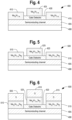
FIG. 5 is a representative side view at a processing step later than that represented inFIG. 4 . -
FIG. 6 is a representative side view illustrating completion of the fabrication of the example shown inFIG. 4 . -
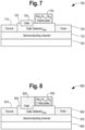
FIG. 7 is a representative side view illustrating an embodiment in accordance with the present invention -
FIG. 8 is a representative side view illustrating a further example. -
FIG. 9 is a flow diagram illustrating steps that can be used in the fabrication of an embodiment in accordance with the present invention. -
FIG. 10 is schematic diagram showing an exemplary circuit that can be used to supply a voltage differential that will produce a field sufficient to control the phase of the phase change material as used in an FET embodiment according to the present invention. -
FIG. 11 is schematic diagram showing an exemplary circuit that can be used to supply a voltage differential that will produce a field sufficient to control the phase of the phase change material used as an ON/OFF semiconductor switch. -
FIG. 1 shows a top view of an example of a representativesemiconductor switch device 100. Aconventional substrate 105, e.g. a silicon, GaAs, InP, SiC, sapphire substrate, such as commonly used in the manufacture of field effect transistors (FETs), has disposed thereon ametallic regions interconnects phase change region 130 which is disposed as a longitudinal strip on the top surface of the substrate betweeninterconnects metallic regions phase change region 130. Theregions phase change region 130 to control whether the phase change material is in the metal or insulating phase which corresponds to current flow or no current flow fromcontact 120 to contact 125. -
Metallic regions phase change region 130.Metallic regions switch 100, such as when a predetermined voltage equal to or greater than the required phase change voltage is or is not applied across the plates by a voltage source (not shown), e.g. a DC or AC voltage source. The electric field developed between the plates when the predetermined voltage is applied provides sufficient energy via the corresponding electric field to cause the phase change region to change from one of an insulator and metal phase to the other phase. When no voltage (or a voltage less than required phase change voltage) is applied to the plates, the other phase is present. The phase change material can be fabricated to have a stable static state of either the insulator phase or the metal phase. The insulator phase corresponds to the switch being OFF and the metal phase corresponds to the switch being ON. This operation of theswitch 100 occurs while the switch temperature remains substantially constant at about room temperature and requires no pressure change to facilitate the switch operation. - The
phase change region 130 preferably consists of MoxW1-xTe2 which can change between an insulator and metal phase based on the presence or absence of an electric field produced by a voltage differential of a few volts, e.g. about 0.5 to 5 volts. This operation does not require a change of temperature or change of pressure. Effective operation of theswitch 100 is possible using MoxW1-xTe2 where the x in the formula varies between 0.66 and 1.0. The ratio between Mo and W as well as the distance between the control electrodes determines the electric field required to cause a phase change. -
FIG. 2 is a side view of another example of aswitch 200 in accordance with the present invention. Onsubstrate 205 is disposed a metallicswitch control contact 210. Adielectric layer 215 covers the top surface of thesubstrate 205. Aregion 220 of phase change material is disposed on the top surface of the dielectric 215 substantially opposite theswitch control contact 210.Conductive interconnects phase change material 220. These interconnects provide conductivity and facilitate the connection of theswitch 200 as an element in a circuit with external components (not shown). Adielectric layer 235 is disposed over the top surface of thephase change region 220 and provides a support for metallicswitch control contact 240. Similar to the operation explained for the embodiment ofFIG. 1 , an electric field induced by a voltage connected acrossswitch control contacts phase change material 220 which in turn determines if the switch will be in the ON state if in the metal phase or will be in the OFF state if in the insulating phase. The switch control contacts form a sandwich with thephase change region 220 therebetween. -
FIG. 3 shows agraph 300 illustrating an exemplary change of current flow on the y-axis 305 versus changes in a control voltage on thex-axis 310 for asemiconductor 100 where the change of phase of MoxW1-xTe2 is used to control the OFF/ON states of the semiconductor. For this example, the x in MoxW1-xTe2 may be between 1 and 0.66. - Starting with a control voltage of 0 and increasing to a voltage at 315 (about 0.5-5 volts), the current flow through the respective device has a moderate increase of about 1 decade, i.e. 10 times, to just over 1E-08 amperes. However, a very small further increase in the control voltage from 315 to 320 (about a 30 - 50 millivolts change) causes over a 3 decade increase in current flow to about 1E-05 amperes. Further increases in the control voltage result in only marginal additional current flow as shown.
- Starting with a control voltage of above 320 and decreasing to a voltage at 325, the current flow through the respective device has a moderate decrease of current flow as shown. However, a very small further decrease in the control voltage from 325 to 330 (about a 30 - 50 millivolts change) causes over a 3 decade decrease in current flow to about 1E-08 amperes. Further decreases in the control voltage result in a further current flow decrease of about 1 decade to 1E-09 amperes as shown. It will be apparent that a hysteresis loop as shown exists between OFF/ON and ON/OFF phase transitions.
- It is important to understand that switches/transistors as described in these examples provide very steep switching transitions of about 30 - 50 millivolts (VGS or voltage across switch 100)/decade of current change (IDS or current flow through the phase change region in switch 100). This offers a substantial improvement of higher speeds of switching state transitions as compared with the switching transition of a conventional silicon FET which has a switching transition of greater than 60 millivolt/decade of current change. As will be understood by those skilled in the art, a faster switching time for a device also corresponds in the analog frequency domain to improved higher frequency performance such as when such a device is utilized as an analog RF amplifier.
-
FIGs. 4, 5 and 6 show side views of an example a semiconductor device utilizing MoxW1-xTe2 illustrating thesemiconductor device FIG. 4 , theembodiment 400 includes asemiconducting channel 405 of a typical semiconductor such as Si, GaAs, InGaAs, or GaN disposed on asubstrate 408 such as Si, GaAs, InP, sapphire and SiC. Asource region 410 and a spaced apart drainregion 415 are deposited on the top surface of thesemiconducting channel 405. A dielectric 420 is disposed on the top of thesemiconducting channel 405 between the source and drain. Agate region 425 is deposited on top of the dielectric 420 between and not engaging the source and drain regions. The source, gate and drain regions are each formed by depositing alloy metals Mo and W as MoxW1-x. These metals can either be co-deposited or a superlattice can be formed, i.e. thin films of the combination repeated one after another. The choice of "x" in the composition is one factor in controlling the magnitude of the electric field needed to cause a phase change. - In an example, the source is fabricated to require a lower magnitude electric field, to cause a phase transition, e.g. a higher W concentration such as 0.2-0.3 with respective x values of 0.8 - 0.7. The gate may be fabricated to require a higher magnitude electric field to cause the phase transition, e.g. a W concentration such as 0 - 0.1 with corresponding X values of 1 - 0.9. The drain may be fabricated to require a higher magnitude electric field to cause the phase transition utilizing the same ratios described for the gate.
-
FIG. 5 shows thesemiconductor device 500 that results from thesemiconductor device 400 having thesource 410,gate 425 and thedrain 415 exposed to a vaporized concentration of Te. The vapor of Te is preferably deposited at an elevated temperature of 400-1200°C which will determine the phase at room temperature with no electric field applied. With Te having been fully reacted, thesemiconductor device 500 will have asource 510,gate 525 and drain 515. -
FIG. 6 shows thesemiconductor device 600 in which conventional metal layers/pads source 510,gate 525 and drain 515. These metal layers facilitate the attachment/bonding of wires/runners to the respective terminals of thesemiconductor device 600 in order to connect the device to external circuitry. Thus,semiconductor device 600 illustrates a completed, fabricated device ready for operation as a steep transition digital switch or in an analog mode as a high-frequency amplifier. -
FIG. 7 shows a side view of anembodiment 700 of a semiconductor in accordance with the present invention. Thesemiconductor 700 represents a conventional semiconductor FET improved with a modification as will be explained. Aconventional substrate 705 has disposed thereon asemiconducting channel 710. Aconventional source 715 and spaced apart drain 720 are disposed on top of thesemiconducting channel 710. Between the source and drain is disposed agate dielectric 725 onto which themetallic gate 730 is deposited between the source and drain, and typically closer to the source than the drain. A layer ofphase change material 735 is deposited on top of thegate dielectric 725 spaced apart between thegate 730 and thedrain 720. During operation, the changing electric field between the gate and drain will cause thephase change layer 735 made of MoxW1-xTe2 to convert between metal and insulator. In the metal phase this extended shield plate will screen traps that can form between the gate and drain, as designated by xxx in the figure. In the insulating phase theshield plate 735 is no longer electrically conducting and avoids parasitic short channel effects typically seen when using a fully metallic shield plate layer between gate and drain -
FIG. 8 shows a side view of another example 800 of a semiconductor. Thesemiconductor 800 represents a conventional FET improved with another modification as will be explained. Aconventional substrate 805 has disposed thereon asemiconducting channel 810. Aconventional source 815 and spaced apart drain 820 are disposed on top of thesemiconducting channel 810. Between the source and drain is disposed agate dielectric 825 onto which themetallic gate 830 is deposited between the source and drain, and typically closer to the source than the drain. A layer ofphase change material 835 is deposited on top of thegate dielectric 825 connected to the edge of thegate 830 closest to the drain and extending laterally towards, but not engaging, thedrain 820. A field applied between the gate and drain region can be utilized to turn the gate extension, provided by thephase change material 835, ON and OFF. In the OFF state the phase change material functions as an insulator making the effective area of the gate only the area occupied bygate 830 which is physically short providing for improved high-frequency response. In the ON state the phase change material functions as a metal that makes the effective gate the combined combination ofgate 830 andphase change material 835 providing a longer effective gate in which the phase change extension functions as a shield trap at the channel surface improving breakdown and mitigating short channel effects. -
FIG. 9 shows a flow diagram illustrating steps that can be used in the fabrication of an embodiment of a FET semiconductor in accordance with the present invention. In step 905 a conventional semiconductor FET structure is fabricated but without the normal metal contacts that would be deposited to make for easier connections with the terminals of the device. In step 910 a layer of MoxW1-x is deposited on the source, drain and gate regions. This phase change material may be deposited by the concurrent deposition of Mo and W, or thin monolayers of each may be alternately deposited. The ratio of W to Mo may be controlled to establish the static phase at room temperature with no electric field applied. The application of an appropriate electrical field, e.g. such as by a voltage differential, to the phase change material will cause a phase change: metal to insulator, or insulator to metal. Useful ratios and corresponding X values in the formula have been discussed previously. Instep 915 the layer of phase change material has deposited thereon Te such as by exposing the exposed surface of the phase change material to a vapor of Te at elevated temperature. Generally, Te deposited using temperatures between 400 and 600 °C result in a phase change material having an insulating state at room temperature operation and using temperatures between 650 and 1,100 °C result in a phase change material having a metal state at room temperature operation. In afinal step 920, a layer of a metal is deposited on the phase change layers providing for source/drain/gate connection contacts. -
FIG. 10 shows a schematic diagram of circuitry in accordance with the present invention that can be used to supply a voltage differential that will produce a field sufficient to control the phase of the phase change material as used in anFET 1005. TheFET 1005 includes adrain 1010,gate 1015 andsource 1020. An additional control gate/terminal 1025 is made of a phase change material as previously described herein. Thegate 1025 is a schematic representation ofelement 735 as shown inFIG. 7 . ADC voltage source 1030 supplies current to thedrain 1010 through theload 1035, assuming that theFET 1005 is in an active/ON state. As will be appreciated, the drain current flows through the semiconducting channel of the FET and out ofsource 120 throughcircuit element 1040 to ground completing the circuit back to thevoltage source 1030. A variableDC voltage source 1045 provides an operational gate voltage to thegate 1015 through isolatingcircuit element 1050. AnAC signal source 1055 is coupled to thegate 1015 through isolatingcircuit element 1060. Depending upon the gain ofFET 1005, the signal from theAC signal source 1055 will appear in an amplified magnitude at thedrain 1010. - In accordance with an embodiment of the present invention, a variable
DC voltage source 1065 is coupled through isolatingcircuit element 1070 to theadditional control gate 1025 which is made of phase change material. The advantages of controlling the semiconducting and insulator phases of the phase change material of varying the voltage applied by thevoltage source 1065 is explained with regard toFIG. 7 and FIG. 8 . TheDC voltage source 1065 has a sufficient voltage range to provide the predetermined phase change voltage level required to transition the phase change material between the metal and insulator phases. -
FIG. 11 shows a schematic diagram of an exemplary circuit that can be used to supply a voltage differential that will produce a field sufficient to control the phase of the phase change material used as an ON/OFF semiconductor switch 1100. In this exemplary embodiment, achannel 1105 is made of a phase change material as described herein. Ametallic contact channel 1105 to permit the attachment of connectingwires switch 1100.Dielectric layers channel 1105.Metallic pads dielectric layers channel 1105. A variableDC voltage source 1150 is connected across themetallic pads source 1150 creates a corresponding internal electric field that is induced upon the lateral sides of thechannel 1105. As previously explained, the phase change material utilized forchannel 1105 will, with no voltage applied bysource 1150, be in one of a metal and insulator phase. With sufficient voltage applied bysource 1150 to reach a predetermined phase change voltage level, the phase change material utilized forchannel 1105 will transition to the other of the metal and insulator phases. Thus, thesemiconductor switch 1100 can be controllably switched between an ON state when thechannel 1105 is in the metal phase and an OFF state when thechannel 1105 is in the insulator phase. As previously explained, the transition between ON/OFF states can be achieved in a shorter time frame than conventional switches based on silicon technology. - Although exemplary implementations of the invention have been depicted and described in detail herein, it will be apparent to those skilled in the art that various modifications, additions, substitutions, and the like can be made without departing from the invention as defined in the following claims.
Claims (5)
- A field effect transistor (FET) apparatus comprising:
an FET device (400; 500; 600; 700; 1005) including:a semiconducting channel (405; 710; 810; 1105);spaced apart source (410; 510; 715; 815; 1020) and drain (415; 515; 720; 820; 1010) regions disposed on a surface of the semiconducting channel;a dielectric layer (420; 725; 825; 1130) disposed on the surface of the semiconducting channel between the source and drain regions;a gate region (425; 525; 730; 830; 1015) disposed on a surface of the dielectric layer opposite the surface of the semiconducting channel and between the source and drain regions;the source, gate and drain regions each being a metallic region;a control region (735; 1025) disposed on the surface of the dielectric layer between the gate region and the drain region, the control region not connected to the gate region, the control region comprising MoxW1-xTe2 phase change material which has a semiconductor phase and an insulator phase selectable based on whether a control voltage field, which is independent from a field produced by a voltage applied at the drain region, is or is not present across the control region;the control region in the semiconductor phase functioning as a shield to passivate traps at the surface of the semiconducting channel between the gate region and the drain region;the control region in the insulator phase enhancing high frequency response of the FET by not presenting a physically active region adjacent the gate region; the phase change material being changed from one of semiconductor and insulator phases to the other of semiconductor and insulator phases at room temperature dependent on whether a voltage differential greater than a predetermined phase change voltage exists across the phase change material. - The FET apparatus of claim 1 further comprising:first and second contacts connected to the gate region and the control region, respectively;first and second voltage sources (1045, 1065) coupled to the first and second contacts, respectively, the first voltage source (1045) determining an operating voltage of the gate region to source region, the second voltage source (1065) providing a control voltage to the control region (735; 1025), one voltage of the second voltage source causing the control region to be in the semiconductor phase and another voltage of the second voltage source causing the control region to be in the insulator phase.
- The FET apparatus of claim 1 wherein the gate region and the control region do not abut each other and are spaced apart.
- The FET apparatus of claim 1 wherein the x in the material composition formula is a positive number less than or equal to 1.0, the value of x differing for the material utilized in the source and gate regions with the source region having a lower x value than the x value for the gate region.
- The FET apparatus of claim 1 wherein the value of x in the material composition formula for the respective regions is as follows:for the source region, 0.7 < x < 0.8,for the gate region, 0.9 < x < 1.0,for the drain region, 0.9 < x < 1.0.
Priority Applications (1)
| Application Number | Priority Date | Filing Date | Title |
|---|---|---|---|
| EP24179818.0A EP4401149A3 (en) | 2019-01-22 | 2019-11-20 | Semiconductor devices using semiconductor-metal phase change materials |
Applications Claiming Priority (2)
| Application Number | Priority Date | Filing Date | Title |
|---|---|---|---|
| US16/254,218 US10811601B2 (en) | 2019-01-22 | 2019-01-22 | Semiconductor devices using insulator-metal phase change materials and method for fabrication |
| PCT/US2019/062377 WO2020154028A1 (en) | 2019-01-22 | 2019-11-20 | Semiconductor devices using insulator-metal phase change materials |
Related Child Applications (1)
| Application Number | Title | Priority Date | Filing Date |
|---|---|---|---|
| EP24179818.0A Division EP4401149A3 (en) | 2019-01-22 | 2019-11-20 | Semiconductor devices using semiconductor-metal phase change materials |
Publications (2)
| Publication Number | Publication Date |
|---|---|
| EP3915154A1 EP3915154A1 (en) | 2021-12-01 |
| EP3915154B1 true EP3915154B1 (en) | 2024-07-03 |
Family
ID=68835387
Family Applications (2)
| Application Number | Title | Priority Date | Filing Date |
|---|---|---|---|
| EP24179818.0A Pending EP4401149A3 (en) | 2019-01-22 | 2019-11-20 | Semiconductor devices using semiconductor-metal phase change materials |
| EP19817555.6A Active EP3915154B1 (en) | 2019-01-22 | 2019-11-20 | Semiconductor devices using semiconductor-metal phase change materials |
Family Applications Before (1)
| Application Number | Title | Priority Date | Filing Date |
|---|---|---|---|
| EP24179818.0A Pending EP4401149A3 (en) | 2019-01-22 | 2019-11-20 | Semiconductor devices using semiconductor-metal phase change materials |
Country Status (6)
| Country | Link |
|---|---|
| US (2) | US10811601B2 (en) |
| EP (2) | EP4401149A3 (en) |
| JP (2) | JP2022517129A (en) |
| KR (1) | KR102772338B1 (en) |
| SG (1) | SG11202107020WA (en) |
| WO (1) | WO2020154028A1 (en) |
Families Citing this family (3)
| Publication number | Priority date | Publication date | Assignee | Title |
|---|---|---|---|---|
| US11805711B2 (en) * | 2020-09-28 | 2023-10-31 | International Business Machines Corporation | Phase-change memory (PCM) including liner reducing resistance drift |
| KR102897071B1 (en) * | 2022-06-10 | 2025-12-16 | 한국과학기술원 | Electronic device including ferroelectric thin film |
| KR102810561B1 (en) * | 2022-09-16 | 2025-05-23 | 한국과학기술원 | Semiconductor device |
Family Cites Families (13)
| Publication number | Priority date | Publication date | Assignee | Title |
|---|---|---|---|---|
| US5461250A (en) | 1992-08-10 | 1995-10-24 | International Business Machines Corporation | SiGe thin film or SOI MOSFET and method for making the same |
| US7453716B2 (en) * | 2004-10-26 | 2008-11-18 | Samsung Electronics Co., Ltd | Semiconductor memory device with stacked control transistors |
| US7230270B2 (en) * | 2004-11-24 | 2007-06-12 | Taiwan Semiconductor Manfacturing Company, Ltd. | Self-aligned double gate device and method for forming same |
| JP4525928B2 (en) | 2005-12-27 | 2010-08-18 | セイコーエプソン株式会社 | Manufacturing method of semiconductor device |
| WO2008108383A1 (en) * | 2007-03-02 | 2008-09-12 | Nec Corporation | Semiconductor device employing graphene and method for fabricating the same |
| US8896035B2 (en) | 2012-10-22 | 2014-11-25 | International Business Machines Corporation | Field effect transistor having phase transition material incorporated into one or more components for reduced leakage current |
| JPWO2014128990A1 (en) * | 2013-02-19 | 2017-02-02 | 国立研究開発法人産業技術総合研究所 | Phase change channel transistor and driving method thereof |
| JP6421446B2 (en) * | 2013-06-28 | 2018-11-14 | 株式会社リコー | Field effect transistor, display element, image display apparatus and system |
| US9455343B2 (en) * | 2013-09-27 | 2016-09-27 | Intel Corporation | Hybrid phase field effect transistor |
| US9673390B2 (en) * | 2014-02-21 | 2017-06-06 | The Board Of Trustees Of The Leland Stanford Junior University | Phase transformation in transition metal dichalcogenides |
| TWI686874B (en) * | 2014-12-26 | 2020-03-01 | 日商半導體能源研究所股份有限公司 | Semiconductor device, display device, display module, electronic evice, oxide, and manufacturing method of oxide |
| KR102412965B1 (en) * | 2014-12-30 | 2022-06-24 | 삼성전자주식회사 | Electronic device having two dimensional material layer and method of manufacturing the electronic device using inkjet printing |
| US11034847B2 (en) * | 2017-07-14 | 2021-06-15 | Samsung Electronics Co., Ltd. | Hardmask composition, method of forming pattern using hardmask composition, and hardmask formed from hardmask composition |
-
2019
- 2019-01-22 US US16/254,218 patent/US10811601B2/en active Active
- 2019-11-20 EP EP24179818.0A patent/EP4401149A3/en active Pending
- 2019-11-20 WO PCT/US2019/062377 patent/WO2020154028A1/en not_active Ceased
- 2019-11-20 EP EP19817555.6A patent/EP3915154B1/en active Active
- 2019-11-20 KR KR1020217021456A patent/KR102772338B1/en active Active
- 2019-11-20 JP JP2021541541A patent/JP2022517129A/en active Pending
- 2019-11-20 SG SG11202107020WA patent/SG11202107020WA/en unknown
-
2020
- 2020-09-04 US US17/012,400 patent/US11018296B1/en active Active
-
2023
- 2023-10-03 JP JP2023172077A patent/JP7686717B2/en active Active
Also Published As
| Publication number | Publication date |
|---|---|
| JP2022517129A (en) | 2022-03-04 |
| JP2023175906A (en) | 2023-12-12 |
| KR102772338B1 (en) | 2025-02-21 |
| US10811601B2 (en) | 2020-10-20 |
| EP3915154A1 (en) | 2021-12-01 |
| EP4401149A2 (en) | 2024-07-17 |
| KR20210111776A (en) | 2021-09-13 |
| US11018296B1 (en) | 2021-05-25 |
| US20200235293A1 (en) | 2020-07-23 |
| WO2020154028A1 (en) | 2020-07-30 |
| EP4401149A3 (en) | 2024-10-30 |
| JP7686717B2 (en) | 2025-06-02 |
| SG11202107020WA (en) | 2021-08-30 |
Similar Documents
| Publication | Publication Date | Title |
|---|---|---|
| JP7686717B2 (en) | Semiconductor device using insulator-metal phase change material and method for manufacturing the semiconductor device | |
| US6100571A (en) | Fet having non-overlapping field control electrode between gate and drain | |
| JP3827346B2 (en) | Logic circuit having negative differential resistance element and manufacturing method thereof | |
| US3339128A (en) | Insulated offset gate field effect transistor | |
| EP2601680B1 (en) | High electron mobility transistors with field plate electrode | |
| US4972237A (en) | Metal-semiconductor field effect transistor device | |
| EP1964178A2 (en) | Mos transistor and a method of manufacturing a mos transistor | |
| US3409812A (en) | Space-charge-limited current triode device | |
| US6278158B1 (en) | Voltage variable capacitor with improved C-V linearity | |
| US3370184A (en) | Combination of thin-filmed electrical devices | |
| US11611003B2 (en) | Semiconductor component, use of a semiconductor component | |
| WO1995034913A1 (en) | Bootstrapped-gate field effect transistors and circuits thereof | |
| EP0481113B1 (en) | Digitally controlled field effect attenuator devices | |
| US4998147A (en) | Field effect attenuator devices having controlled electrical lengths | |
| JP4272547B2 (en) | Field effect transistor and integrated circuit device and switch circuit using the same | |
| JP3137290B2 (en) | Digitally controlled variable attenuator using field effect device | |
| JP3772562B2 (en) | Semiconductor device | |
| JP2007208036A (en) | Semiconductor element | |
| JPH0354852B2 (en) | ||
| WO2024220067A1 (en) | Iii-n dual gate devices | |
| KR0155302B1 (en) | Thin film field effect transistor | |
| KR20010052109A (en) | InxGa1-xP Stop-Etch Layer for Selective Recess of Gallium Arsenide-based Epitaxial Field Effect Transistors and Process Therefor | |
| Tsurumi et al. | Improved RF characteristics of InGaP/GaAs HBTs by using novel ledge coupled capacitor (LCC) structure | |
| KR20200001880A (en) | Graphene-Silicon Junction Transistor | |
| JPH0468792B2 (en) |
Legal Events
| Date | Code | Title | Description |
|---|---|---|---|
| STAA | Information on the status of an ep patent application or granted ep patent |
Free format text: STATUS: UNKNOWN |
|
| STAA | Information on the status of an ep patent application or granted ep patent |
Free format text: STATUS: THE INTERNATIONAL PUBLICATION HAS BEEN MADE |
|
| PUAI | Public reference made under article 153(3) epc to a published international application that has entered the european phase |
Free format text: ORIGINAL CODE: 0009012 |
|
| STAA | Information on the status of an ep patent application or granted ep patent |
Free format text: STATUS: REQUEST FOR EXAMINATION WAS MADE |
|
| 17P | Request for examination filed |
Effective date: 20210708 |
|
| AK | Designated contracting states |
Kind code of ref document: A1 Designated state(s): AL AT BE BG CH CY CZ DE DK EE ES FI FR GB GR HR HU IE IS IT LI LT LU LV MC MK MT NL NO PL PT RO RS SE SI SK SM TR |
|
| DAV | Request for validation of the european patent (deleted) | ||
| DAX | Request for extension of the european patent (deleted) | ||
| P01 | Opt-out of the competence of the unified patent court (upc) registered |
Effective date: 20230607 |
|
| REG | Reference to a national code |
Ref country code: DE Ref legal event code: R079 Free format text: PREVIOUS MAIN CLASS: H01L0045000000 Ipc: H01L0029080000 Ref country code: DE Ref legal event code: R079 Ref document number: 602019054705 Country of ref document: DE Free format text: PREVIOUS MAIN CLASS: H01L0045000000 Ipc: H01L0029080000 |
|
| RIC1 | Information provided on ipc code assigned before grant |
Ipc: H01L 29/78 20060101ALI20231219BHEP Ipc: H01L 29/417 20060101ALI20231219BHEP Ipc: H01L 29/40 20060101ALI20231219BHEP Ipc: H10N 70/00 20230101ALI20231219BHEP Ipc: H10N 70/20 20230101ALI20231219BHEP Ipc: H01L 21/8234 20060101ALI20231219BHEP Ipc: H01L 21/28 20060101ALI20231219BHEP Ipc: H01L 29/49 20060101ALI20231219BHEP Ipc: H01L 29/08 20060101AFI20231219BHEP |
|
| GRAP | Despatch of communication of intention to grant a patent |
Free format text: ORIGINAL CODE: EPIDOSNIGR1 |
|
| STAA | Information on the status of an ep patent application or granted ep patent |
Free format text: STATUS: GRANT OF PATENT IS INTENDED |
|
| INTG | Intention to grant announced |
Effective date: 20240130 |
|
| GRAS | Grant fee paid |
Free format text: ORIGINAL CODE: EPIDOSNIGR3 |
|
| GRAA | (expected) grant |
Free format text: ORIGINAL CODE: 0009210 |
|
| STAA | Information on the status of an ep patent application or granted ep patent |
Free format text: STATUS: THE PATENT HAS BEEN GRANTED |
|
| AK | Designated contracting states |
Kind code of ref document: B1 Designated state(s): AL AT BE BG CH CY CZ DE DK EE ES FI FR GB GR HR HU IE IS IT LI LT LU LV MC MK MT NL NO PL PT RO RS SE SI SK SM TR |
|
| REG | Reference to a national code |
Ref country code: CH Ref legal event code: EP |
|
| REG | Reference to a national code |
Ref country code: DE Ref legal event code: R096 Ref document number: 602019054705 Country of ref document: DE |
|
| REG | Reference to a national code |
Ref country code: LT Ref legal event code: MG9D |
|
| REG | Reference to a national code |
Ref country code: NL Ref legal event code: MP Effective date: 20240703 |
|
| REG | Reference to a national code |
Ref country code: DE Ref legal event code: R079 Ref document number: 602019054705 Country of ref document: DE Free format text: PREVIOUS MAIN CLASS: H01L0029080000 Ipc: H10D0062130000 |
|
| PG25 | Lapsed in a contracting state [announced via postgrant information from national office to epo] |
Ref country code: PT Free format text: LAPSE BECAUSE OF FAILURE TO SUBMIT A TRANSLATION OF THE DESCRIPTION OR TO PAY THE FEE WITHIN THE PRESCRIBED TIME-LIMIT Effective date: 20241104 |
|
| REG | Reference to a national code |
Ref country code: AT Ref legal event code: MK05 Ref document number: 1700754 Country of ref document: AT Kind code of ref document: T Effective date: 20240703 |
|
| PG25 | Lapsed in a contracting state [announced via postgrant information from national office to epo] |
Ref country code: NL Free format text: LAPSE BECAUSE OF FAILURE TO SUBMIT A TRANSLATION OF THE DESCRIPTION OR TO PAY THE FEE WITHIN THE PRESCRIBED TIME-LIMIT Effective date: 20240703 |
|
| PG25 | Lapsed in a contracting state [announced via postgrant information from national office to epo] |
Ref country code: PT Free format text: LAPSE BECAUSE OF FAILURE TO SUBMIT A TRANSLATION OF THE DESCRIPTION OR TO PAY THE FEE WITHIN THE PRESCRIBED TIME-LIMIT Effective date: 20241104 Ref country code: NL Free format text: LAPSE BECAUSE OF FAILURE TO SUBMIT A TRANSLATION OF THE DESCRIPTION OR TO PAY THE FEE WITHIN THE PRESCRIBED TIME-LIMIT Effective date: 20240703 |
|
| PG25 | Lapsed in a contracting state [announced via postgrant information from national office to epo] |
Ref country code: NO Free format text: LAPSE BECAUSE OF FAILURE TO SUBMIT A TRANSLATION OF THE DESCRIPTION OR TO PAY THE FEE WITHIN THE PRESCRIBED TIME-LIMIT Effective date: 20241003 |
|
| PG25 | Lapsed in a contracting state [announced via postgrant information from national office to epo] |
Ref country code: FI Free format text: LAPSE BECAUSE OF FAILURE TO SUBMIT A TRANSLATION OF THE DESCRIPTION OR TO PAY THE FEE WITHIN THE PRESCRIBED TIME-LIMIT Effective date: 20240703 Ref country code: GR Free format text: LAPSE BECAUSE OF FAILURE TO SUBMIT A TRANSLATION OF THE DESCRIPTION OR TO PAY THE FEE WITHIN THE PRESCRIBED TIME-LIMIT Effective date: 20241004 Ref country code: PL Free format text: LAPSE BECAUSE OF FAILURE TO SUBMIT A TRANSLATION OF THE DESCRIPTION OR TO PAY THE FEE WITHIN THE PRESCRIBED TIME-LIMIT Effective date: 20240703 |
|
| PG25 | Lapsed in a contracting state [announced via postgrant information from national office to epo] |
Ref country code: BG Free format text: LAPSE BECAUSE OF FAILURE TO SUBMIT A TRANSLATION OF THE DESCRIPTION OR TO PAY THE FEE WITHIN THE PRESCRIBED TIME-LIMIT Effective date: 20240703 |
|
| PG25 | Lapsed in a contracting state [announced via postgrant information from national office to epo] |
Ref country code: LV Free format text: LAPSE BECAUSE OF FAILURE TO SUBMIT A TRANSLATION OF THE DESCRIPTION OR TO PAY THE FEE WITHIN THE PRESCRIBED TIME-LIMIT Effective date: 20240703 |
|
| PG25 | Lapsed in a contracting state [announced via postgrant information from national office to epo] |
Ref country code: AT Free format text: LAPSE BECAUSE OF FAILURE TO SUBMIT A TRANSLATION OF THE DESCRIPTION OR TO PAY THE FEE WITHIN THE PRESCRIBED TIME-LIMIT Effective date: 20240703 Ref country code: IS Free format text: LAPSE BECAUSE OF FAILURE TO SUBMIT A TRANSLATION OF THE DESCRIPTION OR TO PAY THE FEE WITHIN THE PRESCRIBED TIME-LIMIT Effective date: 20241103 |
|
| PG25 | Lapsed in a contracting state [announced via postgrant information from national office to epo] |
Ref country code: HR Free format text: LAPSE BECAUSE OF FAILURE TO SUBMIT A TRANSLATION OF THE DESCRIPTION OR TO PAY THE FEE WITHIN THE PRESCRIBED TIME-LIMIT Effective date: 20240703 Ref country code: CZ Free format text: LAPSE BECAUSE OF FAILURE TO SUBMIT A TRANSLATION OF THE DESCRIPTION OR TO PAY THE FEE WITHIN THE PRESCRIBED TIME-LIMIT Effective date: 20240703 |
|
| PG25 | Lapsed in a contracting state [announced via postgrant information from national office to epo] |
Ref country code: ES Free format text: LAPSE BECAUSE OF FAILURE TO SUBMIT A TRANSLATION OF THE DESCRIPTION OR TO PAY THE FEE WITHIN THE PRESCRIBED TIME-LIMIT Effective date: 20240703 Ref country code: RS Free format text: LAPSE BECAUSE OF FAILURE TO SUBMIT A TRANSLATION OF THE DESCRIPTION OR TO PAY THE FEE WITHIN THE PRESCRIBED TIME-LIMIT Effective date: 20241003 |
|
| PG25 | Lapsed in a contracting state [announced via postgrant information from national office to epo] |
Ref country code: RS Free format text: LAPSE BECAUSE OF FAILURE TO SUBMIT A TRANSLATION OF THE DESCRIPTION OR TO PAY THE FEE WITHIN THE PRESCRIBED TIME-LIMIT Effective date: 20241003 Ref country code: PL Free format text: LAPSE BECAUSE OF FAILURE TO SUBMIT A TRANSLATION OF THE DESCRIPTION OR TO PAY THE FEE WITHIN THE PRESCRIBED TIME-LIMIT Effective date: 20240703 Ref country code: NO Free format text: LAPSE BECAUSE OF FAILURE TO SUBMIT A TRANSLATION OF THE DESCRIPTION OR TO PAY THE FEE WITHIN THE PRESCRIBED TIME-LIMIT Effective date: 20241003 Ref country code: LV Free format text: LAPSE BECAUSE OF FAILURE TO SUBMIT A TRANSLATION OF THE DESCRIPTION OR TO PAY THE FEE WITHIN THE PRESCRIBED TIME-LIMIT Effective date: 20240703 Ref country code: IS Free format text: LAPSE BECAUSE OF FAILURE TO SUBMIT A TRANSLATION OF THE DESCRIPTION OR TO PAY THE FEE WITHIN THE PRESCRIBED TIME-LIMIT Effective date: 20241103 Ref country code: HR Free format text: LAPSE BECAUSE OF FAILURE TO SUBMIT A TRANSLATION OF THE DESCRIPTION OR TO PAY THE FEE WITHIN THE PRESCRIBED TIME-LIMIT Effective date: 20240703 Ref country code: GR Free format text: LAPSE BECAUSE OF FAILURE TO SUBMIT A TRANSLATION OF THE DESCRIPTION OR TO PAY THE FEE WITHIN THE PRESCRIBED TIME-LIMIT Effective date: 20241004 Ref country code: FI Free format text: LAPSE BECAUSE OF FAILURE TO SUBMIT A TRANSLATION OF THE DESCRIPTION OR TO PAY THE FEE WITHIN THE PRESCRIBED TIME-LIMIT Effective date: 20240703 Ref country code: ES Free format text: LAPSE BECAUSE OF FAILURE TO SUBMIT A TRANSLATION OF THE DESCRIPTION OR TO PAY THE FEE WITHIN THE PRESCRIBED TIME-LIMIT Effective date: 20240703 Ref country code: CZ Free format text: LAPSE BECAUSE OF FAILURE TO SUBMIT A TRANSLATION OF THE DESCRIPTION OR TO PAY THE FEE WITHIN THE PRESCRIBED TIME-LIMIT Effective date: 20240703 Ref country code: BG Free format text: LAPSE BECAUSE OF FAILURE TO SUBMIT A TRANSLATION OF THE DESCRIPTION OR TO PAY THE FEE WITHIN THE PRESCRIBED TIME-LIMIT Effective date: 20240703 Ref country code: AT Free format text: LAPSE BECAUSE OF FAILURE TO SUBMIT A TRANSLATION OF THE DESCRIPTION OR TO PAY THE FEE WITHIN THE PRESCRIBED TIME-LIMIT Effective date: 20240703 |
|
| REG | Reference to a national code |
Ref country code: DE Ref legal event code: R097 Ref document number: 602019054705 Country of ref document: DE |
|
| PG25 | Lapsed in a contracting state [announced via postgrant information from national office to epo] |
Ref country code: DK Free format text: LAPSE BECAUSE OF FAILURE TO SUBMIT A TRANSLATION OF THE DESCRIPTION OR TO PAY THE FEE WITHIN THE PRESCRIBED TIME-LIMIT Effective date: 20240703 Ref country code: SM Free format text: LAPSE BECAUSE OF FAILURE TO SUBMIT A TRANSLATION OF THE DESCRIPTION OR TO PAY THE FEE WITHIN THE PRESCRIBED TIME-LIMIT Effective date: 20240703 Ref country code: RO Free format text: LAPSE BECAUSE OF FAILURE TO SUBMIT A TRANSLATION OF THE DESCRIPTION OR TO PAY THE FEE WITHIN THE PRESCRIBED TIME-LIMIT Effective date: 20240703 |
|
| PG25 | Lapsed in a contracting state [announced via postgrant information from national office to epo] |
Ref country code: EE Free format text: LAPSE BECAUSE OF FAILURE TO SUBMIT A TRANSLATION OF THE DESCRIPTION OR TO PAY THE FEE WITHIN THE PRESCRIBED TIME-LIMIT Effective date: 20240703 |
|
| PG25 | Lapsed in a contracting state [announced via postgrant information from national office to epo] |
Ref country code: IT Free format text: LAPSE BECAUSE OF FAILURE TO SUBMIT A TRANSLATION OF THE DESCRIPTION OR TO PAY THE FEE WITHIN THE PRESCRIBED TIME-LIMIT Effective date: 20240703 Ref country code: SK Free format text: LAPSE BECAUSE OF FAILURE TO SUBMIT A TRANSLATION OF THE DESCRIPTION OR TO PAY THE FEE WITHIN THE PRESCRIBED TIME-LIMIT Effective date: 20240703 |
|
| PLBE | No opposition filed within time limit |
Free format text: ORIGINAL CODE: 0009261 |
|
| STAA | Information on the status of an ep patent application or granted ep patent |
Free format text: STATUS: NO OPPOSITION FILED WITHIN TIME LIMIT |
|
| 26N | No opposition filed |
Effective date: 20250404 |
|
| REG | Reference to a national code |
Ref country code: CH Ref legal event code: PL |
|
| PG25 | Lapsed in a contracting state [announced via postgrant information from national office to epo] |
Ref country code: MC Free format text: LAPSE BECAUSE OF FAILURE TO SUBMIT A TRANSLATION OF THE DESCRIPTION OR TO PAY THE FEE WITHIN THE PRESCRIBED TIME-LIMIT Effective date: 20240703 |
|
| PG25 | Lapsed in a contracting state [announced via postgrant information from national office to epo] |
Ref country code: LU Free format text: LAPSE BECAUSE OF NON-PAYMENT OF DUE FEES Effective date: 20241120 |
|
| REG | Reference to a national code |
Ref country code: CH Ref legal event code: PL |
|
| PG25 | Lapsed in a contracting state [announced via postgrant information from national office to epo] |
Ref country code: CH Free format text: LAPSE BECAUSE OF NON-PAYMENT OF DUE FEES Effective date: 20241130 |
|
| REG | Reference to a national code |
Ref country code: BE Ref legal event code: MM Effective date: 20241130 |
|
| PG25 | Lapsed in a contracting state [announced via postgrant information from national office to epo] |
Ref country code: SE Free format text: LAPSE BECAUSE OF FAILURE TO SUBMIT A TRANSLATION OF THE DESCRIPTION OR TO PAY THE FEE WITHIN THE PRESCRIBED TIME-LIMIT Effective date: 20240703 |
|
| PG25 | Lapsed in a contracting state [announced via postgrant information from national office to epo] |
Ref country code: BE Free format text: LAPSE BECAUSE OF NON-PAYMENT OF DUE FEES Effective date: 20241130 |
|
| PG25 | Lapsed in a contracting state [announced via postgrant information from national office to epo] |
Ref country code: IE Free format text: LAPSE BECAUSE OF NON-PAYMENT OF DUE FEES Effective date: 20241120 |
|
| PGFP | Annual fee paid to national office [announced via postgrant information from national office to epo] |
Ref country code: DE Payment date: 20251119 Year of fee payment: 7 |
|
| PGFP | Annual fee paid to national office [announced via postgrant information from national office to epo] |
Ref country code: GB Payment date: 20251121 Year of fee payment: 7 |
|
| PGFP | Annual fee paid to national office [announced via postgrant information from national office to epo] |
Ref country code: FR Payment date: 20251126 Year of fee payment: 7 |
|
| PG25 | Lapsed in a contracting state [announced via postgrant information from national office to epo] |
Ref country code: HU Free format text: LAPSE BECAUSE OF FAILURE TO SUBMIT A TRANSLATION OF THE DESCRIPTION OR TO PAY THE FEE WITHIN THE PRESCRIBED TIME-LIMIT; INVALID AB INITIO Effective date: 20191120 |
|
| PG25 | Lapsed in a contracting state [announced via postgrant information from national office to epo] |
Ref country code: CY Free format text: LAPSE BECAUSE OF FAILURE TO SUBMIT A TRANSLATION OF THE DESCRIPTION OR TO PAY THE FEE WITHIN THE PRESCRIBED TIME-LIMIT; INVALID AB INITIO Effective date: 20191120 |