EP3914906B1 - Kapazitiver sensor - Google Patents
Kapazitiver sensor Download PDFInfo
- Publication number
- EP3914906B1 EP3914906B1 EP20704905.7A EP20704905A EP3914906B1 EP 3914906 B1 EP3914906 B1 EP 3914906B1 EP 20704905 A EP20704905 A EP 20704905A EP 3914906 B1 EP3914906 B1 EP 3914906B1
- Authority
- EP
- European Patent Office
- Prior art keywords
- electrode
- electrical potential
- electrical
- measurement
- potentials
- Prior art date
- Legal status (The legal status is an assumption and is not a legal conclusion. Google has not performed a legal analysis and makes no representation as to the accuracy of the status listed.)
- Active
Links
Images





Classifications
-
- G—PHYSICS
- G01—MEASURING; TESTING
- G01N—INVESTIGATING OR ANALYSING MATERIALS BY DETERMINING THEIR CHEMICAL OR PHYSICAL PROPERTIES
- G01N27/00—Investigating or analysing materials by the use of electric, electrochemical, or magnetic means
- G01N27/02—Investigating or analysing materials by the use of electric, electrochemical, or magnetic means by investigating impedance
- G01N27/22—Investigating or analysing materials by the use of electric, electrochemical, or magnetic means by investigating impedance by investigating capacitance
- G01N27/228—Circuits therefor
-
- G—PHYSICS
- G01—MEASURING; TESTING
- G01D—MEASURING NOT SPECIALLY ADAPTED FOR A SPECIFIC VARIABLE; ARRANGEMENTS FOR MEASURING TWO OR MORE VARIABLES NOT COVERED IN A SINGLE OTHER SUBCLASS; TARIFF METERING APPARATUS; MEASURING OR TESTING NOT OTHERWISE PROVIDED FOR
- G01D5/00—Mechanical means for transferring the output of a sensing member; Means for converting the output of a sensing member to another variable where the form or nature of the sensing member does not constrain the means for converting; Transducers not specially adapted for a specific variable
- G01D5/12—Mechanical means for transferring the output of a sensing member; Means for converting the output of a sensing member to another variable where the form or nature of the sensing member does not constrain the means for converting; Transducers not specially adapted for a specific variable using electric or magnetic means
- G01D5/14—Mechanical means for transferring the output of a sensing member; Means for converting the output of a sensing member to another variable where the form or nature of the sensing member does not constrain the means for converting; Transducers not specially adapted for a specific variable using electric or magnetic means influencing the magnitude of a current or voltage
- G01D5/24—Mechanical means for transferring the output of a sensing member; Means for converting the output of a sensing member to another variable where the form or nature of the sensing member does not constrain the means for converting; Transducers not specially adapted for a specific variable using electric or magnetic means influencing the magnitude of a current or voltage by varying capacitance
-
- G—PHYSICS
- G01—MEASURING; TESTING
- G01N—INVESTIGATING OR ANALYSING MATERIALS BY DETERMINING THEIR CHEMICAL OR PHYSICAL PROPERTIES
- G01N27/00—Investigating or analysing materials by the use of electric, electrochemical, or magnetic means
- G01N27/02—Investigating or analysing materials by the use of electric, electrochemical, or magnetic means by investigating impedance
- G01N27/22—Investigating or analysing materials by the use of electric, electrochemical, or magnetic means by investigating impedance by investigating capacitance
- G01N27/221—Investigating or analysing materials by the use of electric, electrochemical, or magnetic means by investigating impedance by investigating capacitance by investigating the dielectric properties
-
- G—PHYSICS
- G01—MEASURING; TESTING
- G01N—INVESTIGATING OR ANALYSING MATERIALS BY DETERMINING THEIR CHEMICAL OR PHYSICAL PROPERTIES
- G01N27/00—Investigating or analysing materials by the use of electric, electrochemical, or magnetic means
- G01N27/02—Investigating or analysing materials by the use of electric, electrochemical, or magnetic means by investigating impedance
- G01N27/22—Investigating or analysing materials by the use of electric, electrochemical, or magnetic means by investigating impedance by investigating capacitance
- G01N27/223—Investigating or analysing materials by the use of electric, electrochemical, or magnetic means by investigating impedance by investigating capacitance for determining moisture content, e.g. humidity
-
- G—PHYSICS
- G01—MEASURING; TESTING
- G01N—INVESTIGATING OR ANALYSING MATERIALS BY DETERMINING THEIR CHEMICAL OR PHYSICAL PROPERTIES
- G01N27/00—Investigating or analysing materials by the use of electric, electrochemical, or magnetic means
- G01N27/02—Investigating or analysing materials by the use of electric, electrochemical, or magnetic means by investigating impedance
- G01N27/22—Investigating or analysing materials by the use of electric, electrochemical, or magnetic means by investigating impedance by investigating capacitance
- G01N27/226—Construction of measuring vessels; Electrodes therefor
Definitions
- the disclosure relates to a capacitive sensor, in particular a capacitive humidity sensor, a capacitive gas sensor and a capacitive particulate matter sensor. Further aspects of the disclosure relate to a method for capacitive sensing, in particular for capacitive humidity sensing.
- Capacitive sensors may be embodied e.g. as humidity sensors, in particular as sensors for sensing the relative humidity of the environmental air, are widely used in environmental sensing applications.
- One type of humidity sensors are capacitive humidity sensors which comprise one or more humidity sensitive layers, in particular a polymer layer, which are arranged between two electrodes and interact with the environmental air.
- the measured capacity between the two electrodes correlates to the humidity of the environmental air and hence establishes a measure for the humidity.
- capacitive humidity sensors One problem of capacitive humidity sensors is that the environment of the sensing layer may not be well defined. In particular, the impedance of the environment may change in an uncontrolled manner. As an example, in case of condensation of water or another liquid on the humidity sensitive layer or by a contamination of the humidity sensitive layer with particles, the measured capacity may drop below 100%. Such a saturation event may lead to false measurements. In particular, a corresponding sensor may not be able to differentiate between a condensation scenario and a scenario according to which the relative humidity is indeed a bit below 100%.
- one problem to be solved by the present invention is therefore to provide a capacitive sensor with an improved sensitivity range, in particular a humidity sensor that is able to detect condensation scenarios.
- a capacitive humidity sensor comprising a substrate and an electrode structure.
- the electrode structure comprises at least a first electrode and a second electrode and a sensing layer arranged between the first electrode and the second electrode.
- the sensing layer may have in particular a humidity sensitive permittivity and may hence be embodied as humidity sensitive layer.
- the sensor further comprises a measurement circuit configured to measure the capacitance of the electrode structure by applying, at a first measurement phase, a first pair of electrical potentials to the first electrode and the second electrode.
- the first pair of electrical potentials comprises a first electrical potential of the first electrode and a first electrical potential of the second electrode.
- the measurement circuit is further configured to apply, at a second measurement phase, a second pair of electrical potentials to the first electrode and the second electrode.
- the second pair of electrical potentials comprises a second electrical potential of the first electrode and a second electrical potential of the second electrode.
- the embodiment of the first aspect is in particular characterized in that the first electrical potential of the second electrode and the second electrical potential of the second electrode are different from each other.
- V A1 denotes the first electrical potential of the first electrode at the first measurement phase and V A2 denotes the second electrical potential of the first electrode at the second measurement phase.
- V B1 denotes the first electrical potential of the second electrode at the first measurement phase and V B2 denotes the second electrical potential of the second electrode at the second measurement phase.
- C AE is the mutual capacitance between the first electrode and a virtual electrode arranged on the surface of the sensing layer
- C BE is the capacitance between the second electrode and the virtual electrode arranged on the surface of the sensing layer.
- Such an embodied capacitive sensor is configured to measure the capacitance of its electrode structure by means of a 2-phase measurement.
- the 2-phase measurement encompasses a first measurement phase and a second measurement phase during which a specific set of electrical potentials is applied to the first electrode and the second electrode.
- the first electrical potential of the second electrode and the second electrical potential of the second electrode are different from each other.
- the electrical potential of the second electrode changes between the first measurement phase and the second measurement phase.
- Such an embodied sensor provides the advantage that the different electrical potentials of the second electrode may be advantageously used to adapt the sensor functionality for specific measurement scenarios.
- sensors according to embodiments of the invention may be designed in such a way that a condensation on the surface of the sensing layer and/or a contamination of the sensing layer does not result in false measurements.
- the first electrical potential of the first electrode and the second electrical potential of the first electrode are different from each other. This increases the resulting charge difference between the first measurement phase and the second measurement phase.
- the virtual electrode may be considered as an electrode that is used to define and/or measure the capacitances C AE and C BE or more particularly the quotient C AE /C BE .
- the virtual electrode is arranged on the surface of the sensing layer.
- the surface of the sensing layer is the area of the sensing layer that is adjacent to the environmental air. In other words, the surface of the sensing layer provides an interface to the environmental air and interacts with the environmental air.
- the virtual electrode is not physically present during the sensing operation of the sensor.
- the virtual electrode may be applied on the surface of the sensing layer of a sample sensor to determine the quotient C AE /C BE or it may be used to determine the quotient C AE /C BE by means of a simulation.
- the quotient C BE /C AE may be determined in several different ways or methods as generally known to a skilled person in the art.
- the quotient C BE /C AE may be determined by a simulation according to the finite element method (FEM).
- FEM finite element method
- commercially available programs may be used, e.g. the Comsol Multiphysics ® software.
- the FEM simulation derives the quotient C BE /C AE by simulating the geometry of the electrode structure comprising the first electrode, the second electrode and the virtual electrode.
- the quotient C BE /C AE depends only on the geometry of the electrode structure, assuming that the permittivity of the dielectric material between the electrode structure is homogenous.
- the quotient C BE /C AE may be determined by measurement, e.g. by measurements using a capacitive voltage divider formed by the capacitances C AE and C BE .
- the virtual electrode may be provided as real electrode or in other words physically on the surface of the sensing layer, e.g. by applying a conductive layer on the surface of the sensing layer.
- the geometry of the electrode structure remains constant and does not change during the measurement.
- the measured capacitance depends on a property or characteristic of the sensing layer, in particular on a property or characteristic of the material of the sensing layer, in particular on the permittivity of the sensing layer.
- the first pair of electrical potentials and the second pair of electrical potentials are chosen such that leakage currents between the surface of the sensing layer and electrical structures surrounding the surface of the sensing layer are reduced, in particular minimized, in particular in case of a contamination of the surface of the sensing layer or in case of a condensation on the surface of the sensing layer.
- Such electrical structures may be generally any electrical structures surrounding the sensing layer.
- the electrical structures may be in particular an electrical housing and/or electrical lines or electrical circuits of the sensors arranged in the neighbourhood of the sensing layer.
- intermediate electrical potentials of the first electrode and of the second electrode between the first measurement phase and the second measurement phase may have any arbitrary shape, in particular a rectangular shape or a sinusoidal shape.
- the first electrical potential of the first electrode and the second electrical potential of the first electrode are different from each other and the first electrical potential of the second electrode and the second electrical potential of the second electrode are different from each other.
- the sensing signal, in particular the sensed current, of the measurement circuit may be increased.
- the average electrical potential of the first pair of electrical potentials is the same as the average electrical potential of the second pair of electrical potentials.
- This embodiment is in particular suited for sensors having a symmetric electrode structure, i.e. electrode structures according to which the first electrode and the second electrode are arranged symmetrically with respect to the sensing layer and hence have the same distance to the sensing layer.
- the capacitance C AE between the first electrode and the environment and the capacitance C BE between the second electrode and the environment have the same value.
- Embodiments of the invention are based on an insight of the inventors of the present invention that in case of condensation the impedance between the surface of the sensing layer and external electrical structures surrounding the surface of the sensing layer are not infinite anymore and that this may result in a loss of current via this impedance. As a result, this loss of current reduces the current in the second electrode and hence without countermeasures a sensor may not be able to differentiate a condensation scenario from a humidity scenario of less than 100 % humidity.
- Sensors according to embodiments of the invention avoid by a smart choice of pairs of electrical potentials that current is lost to external electrical structures in case of condensation or other contaminations of the surface of the sensing layer. This facilitates the measurement circuit to differentiate between the two scenarios.
- the measurement circuit may be in particular configured to sense a resulting charge difference between the first measurement phase and the second measurement phase at the second electrode. Accordingly, the measurement circuit evaluates the charge difference which accumulates between the first measurement phase and the second measurement phase. In other words, the measurement circuit compares an initial state (charge state at the end of the first measurement phase) with a final state (charge state at the end of the second measurement phase). However, the run of the charging cycles as such does not need to be considered.
- the total capacitance between the first electrode and the second electrode is larger in case of condensation than in cases without condensation. Accordingly, the resulting charge difference measured by a measurement circuit according to embodiments of the invention increases in case of condensation.
- the measurement circuit is configured to transfer the resulting charge difference to a reference capacitor and to measure a resulting voltage at the reference capacitor. According to an embodiment, the measurement circuit is further configured to determine the capacitance of the sensing layer from the resulting voltage.
- the capacitance of the sensing layer may be derived from the reference capacitance, the resulting voltage and the electrical potentials applied during the first and the second measurement phase.
- the measurement circuit comprises an offset capacitor and the measurement circuit is configured to subtract an offset charge from the resulting charge difference.
- Such an embodiment may be used to transfer a charge to the reference capacitor that is symmetric to 0.
- the measurement circuit comprises an integrator, in particular a switched capacitor amplifier.
- the switched capacitor amplifier is configured to integrate the resulting charge difference or in other words to integrate the current flowing through the second electrode when switching from the first measurement phase to the second measurement phase.
- the integrator in particular the switched capacitor amplifier, is embodied as operational amplifier.
- Such a switched capacitor amplifier circuit may be implemented and fabricated in an efficient way.
- the first electrical potential of the first electrode is the same as the second electrical potential of the second electrode and the second electrical potential of the first electrode is the same as the first electrical potential of the second electrode.
- first electrical potential of the first electrode and the second electrical potential of the second electrode are supply voltage potentials and the first electrical potential of the second electrode and the second electrical potential of the first electrode are ground potentials or the first electrical potential of the first electrode and the second electrical potential of the second electrode are ground potentials and the first electrical potential of the second electrode and the second electrical potential of the first electrode are supply voltage potentials.
- Such a simplified set of electrical potentials facilitates an efficient design and fabrication of the measurement circuit, in particular as ground and supply voltage potentials of a corresponding integrated circuit may be used and no further voltage generation or voltage conversion is needed.
- the senor comprises a first metal layer comprising the first electrode and the second electrode and a second metal layer comprising a shielding structure.
- the shielding structure may comprise a plurality of shielding electrodes.
- the shielding structure performs a shielding of electromagnetic fields.
- a shielding structure may provide an etch stop and hence facilitates an efficient fabrication of the sensor.
- the shielding structure is electrically coupled to a ground potential.
- the parasitic capacitance between the second electrode and ground is measured.
- the shielding structure is electrically coupled to the first electrode.
- the parasitic capacitance between the second electrode and ground is measured with a factor of two.
- the shielding structure is electrically coupled to the second electrode.
- the parasitic capacitance between the second electrode and ground is not measured.
- a method for performing a capacitance measurement comprises steps of providing an electrode structure comprising at least a first electrode, a second electrode and a sensing layer arranged between the first electrode and the second electrode.
- the method comprises further steps of measuring the capacitance of the electrode structure by applying, at a first measurement phase, a first pair of electrical potentials to the first electrode and the second electrode and by applying, at a second measurement phase, a second pair of electrical potentials to the first electrode and the second electrode.
- the first pair of electrical potentials comprises a first electrical potential of the first electrode and a first electrical potential of the second electrode.
- the second pair of electrical potentials comprises a second electrical potential of the first electrode and a second electrical potential of the second electrode.
- the first electrical potential of the second electrode and the second electrical potential of the second electrode are different from each other.
- the method further comprises sensing a resulting charge difference between the first measurement phase and the second measurement phase at the second electrode and transferring the resulting charge difference to a reference capacitor.
- the method may comprise steps of measuring a resulting voltage at the reference capacitor and determining the capacitance of the electrode structure from the resulting voltage.
- Fig. 1 shows a cross sectional view of a capacitive sensor 100 according to an embodiment of the invention.
- the capacitive sensor 100 may be in particular embodied as humidity sensor and comprises an electrode structure 10 comprising first electrodes 11 and second electrodes 12.
- the sensor 100 comprises three first electrodes 11 and two second electrodes 12.
- a sensing layer 15 is arranged between the first electrodes 11 and the second electrodes 12.
- the first electrodes 11 are also denoted as electrodes A and the second electrodes 12 are also denoted as electrodes B.
- the electrode structure 10 forms a first or top metal layer 21.
- the sensing layer 15 has a humidity sensitive permittivity and hence the electrode structure 10 has a humidity sensitive capacitance and may comprise or consist of a polymer.
- the sensing layer 15 extends between the first electrodes 11 and the second electrodes 12 and is illustrated with a diagonal pattern.
- the sensor 100 further comprises dielectric layers 18 which provide an electrical insulation between the first metal layer 21 and a second metal layer 22.
- the second metal layer 22 may also be denoted as second last metal layer.
- the second metal layer 22 comprises a plurality of electrodes 23, which may be in particular electrically coupled to a ground potential and accordingly denoted as ground electrodes.
- the second metal layer 22 forms a shielding structure 22. According to other embodiments the second metal layer 22, in particular the electrodes 23, may be coupled to the first electrode 11 or the second electrode 22.
- the sensor 100 comprises a base substrate 14 on which the second metal layer 22, the dielectric layers 18, the first metal layer 21 and the sensing layer 15 are formed.
- the base substrate 14 may be in particular a semiconductor substrate, e.g. a Si-substrate.
- the sensing layer 15 has a surface 31 to a sensing environment 30.
- the sensing environment 30 may be a gas surrounding the sensor, in particular the environmental air.
- the sensing environment 30 is illustrated by a dotted pattern.
- the sensing environment 30 encompasses a local sensing environment 30a near the surface 31 of the sensing layer 15 and a further sensing environment 30b.
- the further sensing environment 30b encompasses the wider or in other words larger area of the sensor and may also be denoted as wider, remote or distant sensing environment. In FIG. 2 the further sensing area 30b is illustrated with a lower density of dots than the local sensing environment 30a.
- the surface 31 of the sensing layer 15 establishes an interface between the sensing layer 15 and the sensing environment 30. Accordingly, the surface 31 may be also denoted as environmental interface 31.
- the environmental air interacts with the sensing layer 15, in particular via the surface 31 of the sensing layer 15. More particularly, humidity of the environmental air diffuses into the sensing layer 15 and thereby changes the permittivity of the sensing layer 15 between adjacent electrodes 11 and 12 and thereby the capacitance of the electrode structure 10. This capacitance change may be measured in order to sense the humidity of the environmental air 30.
- the humidity sensor 100 derives the humidity of the environmental air or more generally of the gaseous environment which surrounds the humidity sensor 100 from the capacitance of the electrode structure 10.
- a measurement circuit may be connected to the first electrodes 11 and the second electrodes 12.
- FIG. 2 shows a partial cross sectional view 200 of a humidity sensor, more particularly a cut-out section 101 of the sensor 100 as shown in FIG. 1 including a schematic illustration of the capacitances to be considered for measurement approaches according to embodiments of the invention.
- FIG. 3 shows a corresponding schematic electrical equivalent circuit 300 of the partial cross sectional view 200 of FIG. 2 .
- the partial cross sectional view 200 and the electrical equivalent circuit 300 comprise a main capacitance C MAIN between the first electrode A and the second electrode B.
- the first electrode A is coupled to an electrical potential V A and the second electrode B to an electrical potential V B .
- the partial cross sectional view 200 and the electrical equivalent circuit 300 comprises a capacitance C AE between the first electrode 11 and a first reference node N E1 on the surface 31 of the sensing layer 15 and a capacitance C BE between the second electrode 12 and a second reference node N E2 on the surface 31 of the sensing layer 15.
- the capacitance C AE may also be defined as the mutual capacitance between the first electrode 11 and a virtual electrode arranged on the surface 31 of the sensing layer 15, while C BE may also be defined as the capacitance between the second electrode 12 and the virtual electrode.
- the capacitance C AE may be denoted as interface capacitance C AE and the capacitance C BE as interface capacitance C BE .
- the electrical equivalent circuit 300 comprises a parasitic capacitance C AP between the electrode A and a fix potential V G of electrode 23, in particular to ground potential, and a parasitic capacitance C BP between the electrode B and the fix potential V G of electrode 23, in particular to the ground potential.
- the electrical equivalent circuit 300 comprises an environmental capacitance C E .
- the environmental capacitance C E may be considered as a capacitance between two fictive "points" of the sensing environment 30, in particular between two fictive points on or on top of the surface 31 of the sensing layer 15, in particular between the reference nodes N E1 and N E2 .
- the environmental capacitance may be also denoted as surface capacitance.
- the electrical equivalent circuit 300 comprises an impedance Z 0A between the first reference node N E1 and a third reference node N E3 and an impedance Z 0B between the second reference node N E2 and the third reference node N E3 .
- the third reference node N E3 is also a fictive node which is coupled to a floating electrical potential V E .
- the impedance Z 0A and the impedance Z 0B may be resistive, capacitive and/or inductive and may be considered as local impedances of the local sensing environment 30a near the surface 31 of the sensing layer 15.
- the impedances Z 0A and Z 0B may change independently from C MAIN , C AE and C BE .
- the electrical equivalent circuit 300 comprises an impedance Z 0 between the third reference node N E3 and a fourth reference node N E4 .
- the fourth reference node N E4 is also a fictive node which is coupled to an electrical potential V 0 .
- the impedance Z 0 may be considered as an impedance between the local sensing environment 30a near the surface 31 of the sensing layer 30 and the further sensing environment 30b of the sensor 100.
- the impedance Z 0 may change independently from C MAIN , C AE , C BE , Z 0A und Z 0B .
- the electrical potential V 0 may be considered as a defined remote electrical potential of the sensor.
- the electrical structures 50 surrounding the surface 31 of the sensing layer 15 are collectively illustrated with a single line.
- the electrical structures 50 may encompass e.g. electrical lines, electronic circuitry or any other electrical structures of the sensor towards which leakage currents I L may occur via the sensing environment 30 in case of a condensation or contamination of the surface of the sensing layer.
- the short-circuiting may be performed e.g. by applying a conductive layer on the surface of the sensing layer.
- a measurement circuit 40 which measures the permittivity of the sensing layer 15 by applying, at a first measurement phase, a first pair of electrical potentials to the first electrode A and the second electrode B. Then, at a second measurement phase, the measurement circuit 40 applies a second pair of electrical potentials to the first electrode A and the second electrode B.
- FIG. 4 shows an electrical equivalent circuit representing a "normal” or in other words regular measurement scenarios without a substantial contamination or condensation of the surface 31 of the sensing layer 15.
- Z 0A , Z 0B , Z 0 max (1/(w*C E ), 1/(w*C AE ), 1/(w*C BE )), wherein w is the excitation frequency of the first electrode and the second electrode.
- the first electrode 11 and the second electrode 12 are electrically connected by a parallel arrangement of the main capacitance C MAIN and a serial arrangement of C AE , C BE and C E .
- i Bn d dt V A ⁇ V B C MAIN + C AE C BE C E C AE C BE + C AE C E + C BE C E + V G ⁇ V B C BP
- d/dt generally denotes the derivative of the applied voltages V A and V B .
- V A and V B the difference between the voltages being applied at the two phases.
- the current i bn and hence the sensor signal or in other words the sensing signal of the measurement circuit may be increased.
- FIG. 5 shows an electrical equivalent circuit representing a contamination or condensation scenario assuming a local or small scale contamination or condensation of the surface 31 of the sensing layer 15.
- a local contamination or condensation scenario it is generally assumed that the absolute value of Z 0A and Z 0B ⁇ 1/(w*C E ), wherein w is the excitation frequency of the first electrode and the second electrode and that the absolute value of Z 0 » Z 0A , Z 0B .
- the first electrode 11 and the second electrode 12 are electrically connected by a parallel arrangement of the main capacitance C MAIN and a serial arrangement of C AE and C BE .
- i Bl d dt V A ⁇ V B C MAIN + C AE C BE C AE + C BE + V G ⁇ V B C BP .
- FIG. 6 shows an electrical equivalent circuit representing a contamination or condensation scenario assuming a large area or large scale contamination or condensation of the surface 31 of the sensing layer 15.
- a large area contamination or condensation encompasses in particular contamination or condensation scenarios which extend beyond the sensing layer 15 and hence may result in leakage currents to the electrical structures 50 surrounding the sensing layer 15.
- i Bg becomes independent of C AE and the current through C BE depends only on d dt V 0 ⁇ V B , but not anymore on d dt V A . .
- i Bg ⁇ i Bn for the electrode current i B of the second electrode a condition as follows is desired: i Bg ⁇ i Bn .
- the current at the second electrode 12 shall be higher in the case of large area contaminations or large area condensations ("global contaminations") than in the normal measurement scenario.
- the sensor would deliver a larger sensor signal in case of large contamination/condensation.
- V 0 remains constant over time.
- This may be e.g. achieved by a suitable arrangement of the electrical circuits, lines and wires of the electrical structures 50 in the surrounding of the electrode structure as known to an electronic circuit design engineer. In particular, it may be achieved by avoiding to place clocked lines near the electrode structure and in particular near the surface of the sensor chip.
- C BE /C E is unknown, changes with the permittivity of the sensing layer and also depends on the permittivity of the sensing environment.
- the quotient C BE /C AE is determined by the geometry of the electrode structure. It does not change over time and also does not change in dependence on the measurand.
- V A1 denotes the first electrical potential of the first electrode 11 at the first measurement phase
- V A2 is the second electrical potential of the first electrode 11 at the second measurement phase
- V B1 is the first electrical potential of the second electrode 12 at the first measurement phase
- V B2 is the second electrical potential of the second electrode 12 at the second measurement phase.
- V A2 , V A2 , V B1 and V B2 are reached at the end of the respective measurement phase.
- the transition from the first to the second measurement phase can have an arbitrary course.
- the average electrical potential of the first pair of electrical potentials is the same as the average electrical potential of the second pair of electrical potentials.
- the average potential of electrode A and B is kept constant during the first measurement phase and the second measurement phase.
- the parasitic capacitance C BP is also measured assuming that the electrodes 23 are on ground potential.
- the quotient C BE /C AE may be determined in several different ways. As mentioned above, such a determination is only needed in case of asymmetric electrode arrangements, while in symmetric electrode arrangements the quotient is 1.
- the quotient C BE /C AE may be determined by a simulation according to the finite element method (FEM), e.g. by the Comsol Multiphysics ® software. For such a simulation a virtual electrode on the surface 31 of the sensing layer 15 is provided.
- FEM finite element method
- the quotient C BE /C AE may be determined by measurements, e.g. by measurements based on a capacitive voltage divider formed by the capacitances C AE and C BE .
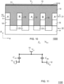
- FIG. 10 shows a cross sectional view of a capacitive sensor 1000, which essentially corresponds to the sensor 100 of FIG. 1 .
- the sensor 1000 however comprises a conductive layer 1010 on the surface 31 of the sensing layer 15.
- the sensor 1000 establishes an exemplary measurement arrangement for measuring the quotient C AE /C BE .
- the conductive layer 1010 establishes a virtual electrode 13.
- the virtual electrode 13 may be considered as a measurement electrode, in particular an auxiliary measurement electrode for measuring the quotient C AE /C BE .
- the conductive layer 1010 may be e.g. a layer of metal that has been applied by spraying or sputtering.
- such a layer may be e.g. a sputtered gold layer (AU layer) having a thickness of e.g. 100nm.
- the gold layer may be connected to an existing pad that can be wire bonded or contacted with probes.
- the conductive layer 1010 may be applied only once or only for one sample sensor in order to determine the quotient C BE /C AE for a corresponding series of sensors.
- the measurement may be performed in a lab environment.
- such a method is in particular useful for asymmetric electrode arrangements, while for symmetric arrangements the quotient C BE /C AE may be assumed to be 1.
- FIG. 11 shows a corresponding electrical equivalent circuit of the exemplary measurement arrangement.
- the electrical equivalent circuit of FIG. 11 does not comprise the capacitances C MAIN , C AP and C BP .
- the latter capacitances may be neglected or omitted as the first electrode 11 and the second electrode 12 are operated for the measurement at defined voltage potentials.
- the corresponding charges Q CAE and Q CBE on the capacitances C AE and C BE are equal to each other.
- one may not measure the quotient C BE /C AE directly, but rather indirectly.
- a relative humidity can be provided e.g. with an appropriate laboratory equipment, e.g. by slowly cooling down a sealed environment (e.g. a sealed box that contains the sensor), until condensation occurs.
- a sealed environment e.g. a sealed box that contains the sensor
- By continuously measuring the sensor capacitance one can determine the difference in the sensors signal just before and after condensation. Such a procedure should be repeated for different levels of VA1, VA2, VB1 and VB2.
- a second measurement is performed where a condensation layer is applied to the sensing layer 30 corresponding to the global contamination/condensation scenario as shown in FIG. 6 .
- a condensation layer may be applied e.g. by applying a thin layer of water on the sensing layer 30.
- the voltage potentials V A1 , V A2 , V B1 and V B2 are then chosen by experiment/trial in such a way that the resulting charge difference at the second electrode is the same for the measurement at a relative humidity of 100% and for the measurement at the global contamination/condensation scenario.
- V A1 2V
- V A2 1V
- the estimated value of the quotient C BE /C AE 0.75.
- V B2 - V B1 sufficiently large, e.g. 3V, so that in any case the product (V B2 -V B1 ) * C BE /C AE ⁇ 1V.
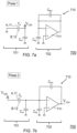
- FIG. 7a and FIG. 7b show a measurement circuit 700 for measuring the capacitance of the sensing layer of sensors according to embodiments of the invention, e.g. of the sensor of FIG. 1 . More particularly, FIG. 7a shows the measurement circuit 700 at the first measurement phase and FIG. 7b the measurement circuit 700 at the second measurement phase.
- the measurement circuit 700 comprises a first circuit part 701 and a second circuit part 702.
- the first circuit part 701 comprises the electrode arrangement with the first electrode A/11, the second electrode B/12 and the sensing layer in between.
- the left circuit part 701 furthermore comprises a voltage generator, which is not shown as such, but only the voltages provided.
- the voltage generator of the measurement circuit 700 provides at the first measurement phase an electrical potential V DD to the second electrode B of the electrode structure and a ground potential to the first electrode A.
- the capacitance to be sensed is denoted with Cs.
- Cs Between the second electrode B and ground there is arranged a parasitic capacitance C P1 .
- the second circuit part 702 forms an integrator 710, in particular a switched capacitor amplifier.
- the integrator 710 is configured to integrate a resulting charge difference as will be explained below.
- the integrator 710 is embodied as switched capacitor amplifier and comprises an operational amplifier 711.
- the positive input of the operational amplifier 711 is coupled to ground.
- a feedback path couples the output of the operational amplifier 711 via an integrating capacitor C INT to the negative (inverting) input of the operational amplifier 711.
- the integrating capacitor C INT may also be denoted as reference capacitor.
- the negative input is coupled via a parasitic capacitance C P2 to ground. In the first measurement phase the integrating capacitor C INT is short circuited.
- the second circuit part 702 is not connected to the first circuit part 701 during the first measurement phase.
- the voltage generator of the measurement circuit provides an electrical potential V DD to the first electrode A of the electrode structure and a ground potential to the second electrode B.
- the second circuit part 702 is during the second measurement phase coupled to the first circuit part 701. More particularly, the negative input of the operational amplifier 711 is coupled to the second electrode B. Hence the ground potential of the second electrode B is provided by the virtual ground of the operational amplifier 711. Furthermore, the integrating capacitor C INT is not short-circuited anymore.
- the measurement circuit 700 may be switched between the first measurement phase and the second measurement phase by appropriate switches as apparent to a skilled person in the art.
- the corresponding switches are not shown in FIG. 7a and FIG 7b for ease of illustration.
- the measurement circuit 700 is configured to transfer a resulting charge difference that results at the second electrode B to the integrating capacitor C INT .
- the integrator 710 integrates a current flowing through the first electrode and the second electrode during the second measurement phase.
- the integrating capacitor C INT forms a reference capacitor.
- the measurement circuit 700 provides a resulting voltage V out at the reference capacitor C INT and the output of the operational amplifier 711. The resulting voltage V out may then be used by the sensor to determine the permittivity of the sensing layer and a corresponding relative humidity.
- FIG. 8a and FIG. 8b show a measurement circuit 800 for measuring the permittivity of the sensing layer of sensors according to embodiments of the invention, e.g. of the sensor of FIG. 1 . More particularly, FIG. 8a shows the measurement circuit 800 at the first measurement phase and FIG. 8b the measurement circuit 800 at the second measurement phase.
- the measurement circuit 800 comprises a first circuit part 701, a second circuit part 702 and a third circuit part 803.
- the circuit parts 701 and 702 correspond to the circuit parts 701 and 702 as shown and described with reference to FIG. 7a and FIG. 7b .
- the third circuit part 803 comprises an offset capacitance C O .
- the offset capacitance C O is charged with the voltage V DD to an offset charge Q O .
- the offset capacitance C O is coupled between ground and the negative input of the operational amplifier 711. Accordingly, the measurement circuit 800 is configured to subtract the offset charge Q O from the resulting charge difference.
- FIG. 9 illustrates a flow chart of method steps of a method for performing a relative humidity measurement.
- the method may be e.g. performed with sensors according to embodiments of the invention as described above.
- an electrode structure which comprises at least a first electrode and a second electrode.
- a sensing layer is provided.
- the sensing layer is arranged between the first electrode and the second electrode and has a humidity sensitive permittivity.
- the first electrode, the sensing layer and the second electrode form a capacitor.
- a first measurement phase is performed and a first pair of electrical potentials is applied to the first electrode and the second electrode.
- a second measurement phase is performed and a second pair of electrical potentials is applied to the first electrode and the second electrode.
- the first pair of electrical potentials comprises a first electrical potential of the first electrode and a first electrical potential of the second electrode.
- the second pair of electrical potentials comprises a second electrical potential of the first electrode and a second electrical potential of the second electrode.
- the first electrical potential of the second electrode and the second electrical potential of the second electrode are different from each other.
- a resulting charge difference between the first measurement phase and the second measurement phase at the second electrode is sensed by a measurement circuit, in particular a readout circuit. More particularly, a change in the charge of the capacitor between the first measurement phase and the second measurement phase results in a current through the first electrode and the second electrode. The current in the second electrode is integrated, resulting in a charge difference seen on the capacitor.
- the resulting charge difference is transferred to a reference capacitor, in particular to a capacitor having a known capacitance.
- a resulting voltage is measured at the reference capacitor.
- the capacitance of the electrode structure may be determined.
- the measured capacitance of the electrode structure is a measure of the humidity of the sensing environment.
- FIG. 12 shows a top view 1200 of the sensor 1000 of FIG. 10 forming an exemplary measurement arrangement for measuring the quotient C AE /C BE according to an embodiment of the invention.
- the virtual electrode 13 which has been applied for measurement purposes covers the whole surface 31 of the sensing layer 15.
- the first electrode 11 and the second electrode 13 are arranged below the virtual electrode 13 and are embodied as interdigitated electrodes.
- FIG. 13 shows a top view 1300 of an exemplary measurement arrangement for measuring the quotient C AE /C BE according to another embodiment of the invention.
- the measurement arrangement 1300 also comprises a virtual electrode 13 covering a sensing layer of a sensor according to an embodiment of the invention.
- the first electrode 11 and the second electrode 12 are not interdigitated electrodes, but have just a simple rectangular shape.
- first electrode and the second electrode may be used for the first electrode and the second electrode according to embodiments.
Landscapes
- Chemical & Material Sciences (AREA)
- General Physics & Mathematics (AREA)
- Physics & Mathematics (AREA)
- Electrochemistry (AREA)
- Health & Medical Sciences (AREA)
- Life Sciences & Earth Sciences (AREA)
- Analytical Chemistry (AREA)
- Biochemistry (AREA)
- General Health & Medical Sciences (AREA)
- Chemical Kinetics & Catalysis (AREA)
- Immunology (AREA)
- Pathology (AREA)
- Investigating Or Analyzing Materials By The Use Of Electric Means (AREA)
- Measurement Of Resistance Or Impedance (AREA)
Claims (13)
- Ein kapazitiver Sensor umfassendein Substrat (14);eine Elektrodenstruktur (10) umfassend
mindestens eine erste Elektrode (11) und eine zweite Elektrode (12); undeine Sensorschicht (15), die zwischen der ersten Elektrode (11) und der zweiten Elektrode (12) angeordnet ist; undeine Messschaltung (40, 500, 600), die so konfiguriert ist, dass siedie Kapazität der Elektrodenstruktur (10) misst, indem siein einer ersten Messphase ein erstes Paar elektrischer Potentiale, das ein erstes elektrisches Potential der ersten Elektrode und ein erstes elektrisches Potential der zweiten Elektrode umfasst, an die erste Elektrode (11) und die zweite Elektrode (12) anlegt; undin einer zweiten Messphase ein zweites Paar elektrischer Potentiale, das ein zweites elektrisches Potential der ersten Elektrode und ein zweites elektrisches Potential der zweiten Elektrode umfasst, an die erste Elektrode (11) und die zweite Elektrode (12) anlegt;
dadurch gekennzeichnet, dassdas erste elektrische Potential der zweiten Elektrode (12) und das zweite elektrische Potential der zweiten Elektrode (12) voneinander verschieden sind;wobei das erste Paar elektrischer Potentiale und das zweite Paar elektrischer Potentiale so angelegt werden, dass
 wobeiVA1 das erste elektrische Potential der ersten Elektrode in der ersten Messphase ist;VA2 das zweite elektrische Potential der ersten Elektrode in der zweiten Messphase ist;VB1 das erste elektrische Potenzial der zweiten Elektrode in der ersten Messphase ist;VB2 das zweite elektrische Potential der zweiten Elektrode in der zweiten Messphase ist;CAE eine Kapazität zwischen der ersten Elektrode und einer virtuellen Elektrode ist, die auf der Oberfläche der Sensorschicht angeordnet ist; undCBE eine Kapazität zwischen der zweiten Elektrode und der virtuellen Elektrode ist, die auf der Oberfläche der Sensorschicht angeordnet ist.
 - Ein Sensor nach Anspruch 1,
wobei das erste Paar elektrischer Potentiale und das zweite Paar elektrischer Potentiale so angelegt werden, dass
- Ein Sensor nach einem der vorangehenden Ansprüche,
wobei das mittlere elektrische Potenzial des ersten Paars elektrischer Potenziale das gleiche ist wie das mittlere elektrische Potenzial des zweiten Paars elektrischer Potenziale. - Ein Sensor nach einem der vorangehenden Ansprüche, wobei die Messschaltung (40, 700, 800) so konfiguriert ist, dass sie
eine resultierende Ladungsdifferenz zwischen der ersten Messphase und der zweiten Messphase an der zweiten Elektrode (12) erfasst. - Ein Sensor nach einem der vorangehenden Ansprüche, wobei die Messschaltung eine geschaltete Kondensatorschaltung und/oder eine geschaltete Stromschaltung umfasst, um das erste und das zweite Paar elektrischer Potenziale zu erzeugen und/oder die resultierende Ladungsdifferenz zu erfassen.
- Ein Sensor nach Anspruch 4 oder 5, wobei die Messschaltung (40, 700, 800) konfiguriert ist, umdie resultierende Ladungsdifferenz zu einem Referenzkondensator (CInt) zu übertragen;eine resultierenden Spannung am Referenzkondensator (CInt) zu messen; unddie Kapazität der Elektrodenstruktur aus der resultierenden Spannung zu bestimmen.
- Ein Sensor nach einem der vorangehenden Ansprüche 4 bis 6, wobeidie Messschaltung (40, 700, 800) einen Offset-Kondensator (CO) umfasst;die Messschaltung (40, 700, 800) so konfiguriert ist, dass sie eine Offset-Ladung von der resultierenden Ladungsdifferenz subtrahiert.
- Ein Sensor nach einem der vorangehenden Ansprüche 4 bis 7, wobei die Messschaltung (40, 700, 800) einen Integrator (710), insbesondere einen Verstärker mit geschalteten Kapazitäten, umfasst, wobei der Integrator (710) so konfiguriert ist, dass er die resultierende Ladungsdifferenz integriert.
- Ein Sensor nach einem der vorangehenden Ansprüche,
wobeidas erste elektrische Potential der ersten Elektrode gleich dem zweiten elektrischen Potential der zweiten Elektrode ist; unddas erste elektrische Potential der zweiten Elektrode gleich dem zweiten elektrischen Potential der ersten Elektrode ist; und insbesondere wobeidas erste elektrische Potential der ersten Elektrode und das zweite elektrische Potential der zweiten Elektrode Versorgungsspannungspotentiale sind; unddas erste elektrische Potential der zweiten Elektrode und das zweite elektrische Potential der ersten Elektrode Massepotentiale sind; oder insbesondere wobei das erste elektrische Potential der ersten Elektrode und das zweite elektrische Potential der zweiten Elektrode Massepotentiale sind; unddas erste elektrische Potenzial der zweiten Elektrode und das zweite elektrische Potenzial der ersten Elektrode Versorgungsspannungspotenziale sind. - Ein Sensor nach einem der vorangehenden Ansprüche, wobei der Sensor Folgendes umfassteine erste Metallschicht (21), die die erste Elektrode (11) und die zweite Elektrode (12) umfasst; undeine zweite Metallschicht (22), die eine Abschirmungsstruktur (22) umfasst.
- Ein Sensor nach Anspruch 10, wobei die Abschirmungsstruktur (22) elektrisch gekoppelt ist anein festes Potential, insbesondere ein Massepotential oder ein Versorgungspotential;die erste Elektrode (11); oderdie zweite Elektrode (12).
- Ein Sensor nach einem der vorangehenden Ansprüche, wobei der Sensor ein kapazitiver Feuchtigkeitssensor, ein kapazitiver Gassensor oder ein kapazitiver Partikelsensor ist.
- Ein Verfahren zur Durchführung einer Kapazitätsmessung, wobei das Verfahren Folgendes umfasstBereitstellen einer Elektrodenstruktur (10), die mindestens eine erste Elektrode (11) und eine zweite Elektrode (12) sowie eine zwischen der ersten Elektrode (11) und der zweiten Elektrode (12) angeordnete Sensorschicht (15) umfasst;Messen der Kapazität der Elektrodenstruktur indemin einer ersten Messphase ein erstes Paar elektrischer Potentiale, das ein erstes elektrisches Potential der ersten Elektrode und ein erstes elektrisches Potential der zweiten Elektrode umfasst, an die erste Elektrode (11) und die zweite Elektrode (12) angelegt wird; undin einer zweiten Messphase ein zweites Paar elektrischer Potenziale, das ein zweites elektrisches Potenzial der ersten Elektrode und ein zweites elektrisches Potenzial der zweiten Elektrode umfasst, an die erste Elektrode (11) und die zweite Elektrode (12) angelegt wird;dadurch gekennzeichnet, dassdas erste elektrische Potential der zweiten Elektrode (12) und das zweite elektrische Potential der zweiten Elektrode (12) voneinander verschieden sind;wobei das erste Paar elektrischer Potentiale und das zweite Paar elektrischer Potentiale so angelegt werden, dass

 wobeiVA1 das erste elektrische Potential der ersten Elektrode in der ersten Messphase ist;VA2 das zweite elektrische Potential der ersten Elektrode in der zweiten Messphase ist;VB1 das erste elektrische Potenzial der zweiten Elektrode in der ersten Messphase ist;VB2 das zweite elektrische Potential der zweiten Elektrode in der zweiten Messphase ist;CAE eine Kapazität zwischen der ersten Elektrode und einer virtuellen Elektrode ist, die auf der Oberfläche der Sensorschicht angeordnet ist; undCBE eine Kapazität zwischen der zweiten Elektrode und der virtuellen Elektrode ist, die auf der Oberfläche der Sensorschicht angeordnet ist.
Applications Claiming Priority (2)
| Application Number | Priority Date | Filing Date | Title |
|---|---|---|---|
| EP19158447.3A EP3699583A1 (de) | 2019-02-21 | 2019-02-21 | Kapazitiver sensor |
| PCT/EP2020/054379 WO2020169676A1 (en) | 2019-02-21 | 2020-02-19 | Capacitive sensor |
Publications (2)
| Publication Number | Publication Date |
|---|---|
| EP3914906A1 EP3914906A1 (de) | 2021-12-01 |
| EP3914906B1 true EP3914906B1 (de) | 2023-05-31 |
Family
ID=65520097
Family Applications (2)
| Application Number | Title | Priority Date | Filing Date |
|---|---|---|---|
| EP19158447.3A Withdrawn EP3699583A1 (de) | 2019-02-21 | 2019-02-21 | Kapazitiver sensor |
| EP20704905.7A Active EP3914906B1 (de) | 2019-02-21 | 2020-02-19 | Kapazitiver sensor |
Family Applications Before (1)
| Application Number | Title | Priority Date | Filing Date |
|---|---|---|---|
| EP19158447.3A Withdrawn EP3699583A1 (de) | 2019-02-21 | 2019-02-21 | Kapazitiver sensor |
Country Status (6)
| Country | Link |
|---|---|
| US (1) | US11726052B2 (de) |
| EP (2) | EP3699583A1 (de) |
| JP (1) | JP7513622B2 (de) |
| KR (1) | KR102838214B1 (de) |
| CN (1) | CN113711024B (de) |
| WO (1) | WO2020169676A1 (de) |
Families Citing this family (1)
| Publication number | Priority date | Publication date | Assignee | Title |
|---|---|---|---|---|
| US11946892B1 (en) | 2021-04-12 | 2024-04-02 | Enco Electronic Systems, Llc | System for and method of improving accuracy and discrimination of liquids in capacitive moisture sensors |
Family Cites Families (20)
| Publication number | Priority date | Publication date | Assignee | Title |
|---|---|---|---|---|
| US3030949A (en) | 1958-08-01 | 1962-04-24 | James S Gassaway | Body manipulating apparatus |
| JPH0687048B2 (ja) * | 1983-10-12 | 1994-11-02 | 株式会社日立製作所 | 有機高分子式湿度センサの動作回路 |
| JP3453962B2 (ja) * | 1995-10-31 | 2003-10-06 | 松下電工株式会社 | 静電容量型雨センサ |
| DE19757190A1 (de) * | 1997-12-22 | 1999-06-24 | Abb Research Ltd | Kapazitiver Füllstandssensor mit integrierter Schmutzfilmdetektion |
| DE19917717C2 (de) * | 1999-04-20 | 2002-10-17 | Joerg Mueller | Kapazitiver Feuchtesensor |
| JP4501320B2 (ja) * | 2001-07-16 | 2010-07-14 | 株式会社デンソー | 容量式湿度センサ |
| EP1411349B1 (de) | 2002-10-18 | 2005-12-21 | Siemens Schweiz AG | Feuchtigkeitsfühler mit kapazitivem Feuchte-Messelement und Verfahren zur Erfassung der Luftfeuchtigkeit |
| JP3855950B2 (ja) | 2003-03-19 | 2006-12-13 | 株式会社デンソー | 容量式湿度センサ |
| JP4229885B2 (ja) * | 2004-08-18 | 2009-02-25 | 株式会社デンソー | 容量式物理量検出装置 |
| JPWO2007063573A1 (ja) * | 2005-11-29 | 2009-05-07 | 富士通マイクロエレクトロニクス株式会社 | 半導体装置とその製造方法 |
| DE102006034931A1 (de) | 2006-07-28 | 2008-01-31 | E + E Elektronik Ges.M.B.H. | Schaltungsanordnung und Verfahren zur Feuchtmessung |
| US8410562B2 (en) * | 2010-01-22 | 2013-04-02 | Carnegie Mellon University | Methods, apparatuses, and systems for micromechanical gas chemical sensing capacitor |
| US20140026642A1 (en) * | 2012-07-25 | 2014-01-30 | John O. O'Connell | Capacitive sensor comprising differing unit cell structures |
| EP2799891A1 (de) * | 2013-05-03 | 2014-11-05 | Sensirion AG | Sensorschaltungsanordnung |
| EP3375892B1 (de) | 2013-12-12 | 2020-07-01 | Altratech Limited | Kapazitiver sensor |
| DE202013105955U1 (de) | 2013-12-27 | 2014-01-20 | Sensirion Ag | Sensorbaustein |
| DE102014202248A1 (de) * | 2014-02-07 | 2015-08-27 | Robert Bosch Gmbh | Sensor zum Detektieren mindestens eines Mediums und Verfahren zum Betreiben einer kapazitiven Messeinrichtung |
| KR102238937B1 (ko) * | 2014-07-22 | 2021-04-09 | 주식회사 키 파운드리 | 배선 사이의 중공에 형성된 습도 센서 및 그 제조 방법 |
| US9696272B2 (en) | 2015-08-07 | 2017-07-04 | Silicon Laboratories Inc. | Systems and methods for humidity measurement using dielectric material-based relative humidity sensors |
| JP6772670B2 (ja) * | 2016-08-26 | 2020-10-21 | アイシン精機株式会社 | 静電容量センサ |
-
2019
- 2019-02-21 EP EP19158447.3A patent/EP3699583A1/de not_active Withdrawn
-
2020
- 2020-02-19 CN CN202080024783.0A patent/CN113711024B/zh active Active
- 2020-02-19 US US17/431,480 patent/US11726052B2/en active Active
- 2020-02-19 JP JP2021549278A patent/JP7513622B2/ja active Active
- 2020-02-19 WO PCT/EP2020/054379 patent/WO2020169676A1/en not_active Ceased
- 2020-02-19 KR KR1020217029842A patent/KR102838214B1/ko active Active
- 2020-02-19 EP EP20704905.7A patent/EP3914906B1/de active Active
Also Published As
| Publication number | Publication date |
|---|---|
| WO2020169676A1 (en) | 2020-08-27 |
| JP2022523359A (ja) | 2022-04-22 |
| KR102838214B1 (ko) | 2025-07-25 |
| US20220136991A1 (en) | 2022-05-05 |
| KR20210127232A (ko) | 2021-10-21 |
| CN113711024A (zh) | 2021-11-26 |
| JP7513622B2 (ja) | 2024-07-09 |
| EP3914906A1 (de) | 2021-12-01 |
| US11726052B2 (en) | 2023-08-15 |
| CN113711024B (zh) | 2024-07-23 |
| EP3699583A1 (de) | 2020-08-26 |
Similar Documents
| Publication | Publication Date | Title |
|---|---|---|
| US9721140B2 (en) | Sensing method of fingerprint sensor and related sensing circuit | |
| KR100363287B1 (ko) | 매우 낮은 커패시턴스를 결정하는 방법과 그것에 관한사용 | |
| US6145384A (en) | Capacitive transducer having guard electrode and buffer amlifying means | |
| US9613247B2 (en) | Sensing method and circuit of fingerprint sensor | |
| EP3346248B1 (de) | Verbesserte druckregler-sensorstruktur | |
| KR101861114B1 (ko) | 플라잉 캐패시터식 전압 검출 회로 및 전지 보호용 집적 회로 | |
| KR20040111631A (ko) | 반도체 장치, 소스와 드레인 사이의 전압차 측정 방법 및반도체 장치 보호 방법 | |
| EP0980004B1 (de) | Mikroskopische Kapazitätmesssystem und Testsystem | |
| EP3914906B1 (de) | Kapazitiver sensor | |
| KR100341966B1 (ko) | 임피던스-전압 변환기 및 변환방법 | |
| KR20150110717A (ko) | 전압 측정 장치 | |
| JP2004184307A (ja) | 静電容量検出回路及び静電容量検出方法 | |
| JP2001512836A (ja) | 非常に小さな容量を求めるための方法およびこれにより構想されたセンサ | |
| JP3815771B2 (ja) | 静電容量式ギャップセンサ、及びその信号検出方法 | |
| JP5066687B2 (ja) | 微小伝導領域のインピーダンス測定回路、ならびに微小伝導領域のインピーダンス測定方法 | |
| JP2003130893A (ja) | シールドを有する電気回路 | |
| JP3311309B2 (ja) | 半導体装置の評価方法 | |
| CN115453205B (zh) | 可克服分布参数及线路电阻影响的高精度阻抗检测电路 | |
| JP3362639B2 (ja) | 半導体装置の絶縁膜の電気的評価装置 | |
| CN107228986A (zh) | 一种电容失配检测电路及方法 | |
| TWI559232B (zh) | 指紋感測器的感測方法及電路 | |
| JPS6341040A (ja) | 半導体集積回路装置 |
Legal Events
| Date | Code | Title | Description |
|---|---|---|---|
| STAA | Information on the status of an ep patent application or granted ep patent |
Free format text: STATUS: UNKNOWN |
|
| STAA | Information on the status of an ep patent application or granted ep patent |
Free format text: STATUS: THE INTERNATIONAL PUBLICATION HAS BEEN MADE |
|
| PUAI | Public reference made under article 153(3) epc to a published international application that has entered the european phase |
Free format text: ORIGINAL CODE: 0009012 |
|
| STAA | Information on the status of an ep patent application or granted ep patent |
Free format text: STATUS: REQUEST FOR EXAMINATION WAS MADE |
|
| 17P | Request for examination filed |
Effective date: 20210823 |
|
| AK | Designated contracting states |
Kind code of ref document: A1 Designated state(s): AL AT BE BG CH CY CZ DE DK EE ES FI FR GB GR HR HU IE IS IT LI LT LU LV MC MK MT NL NO PL PT RO RS SE SI SK SM TR |
|
| DAV | Request for validation of the european patent (deleted) | ||
| DAX | Request for extension of the european patent (deleted) | ||
| GRAP | Despatch of communication of intention to grant a patent |
Free format text: ORIGINAL CODE: EPIDOSNIGR1 |
|
| STAA | Information on the status of an ep patent application or granted ep patent |
Free format text: STATUS: GRANT OF PATENT IS INTENDED |
|
| INTG | Intention to grant announced |
Effective date: 20221219 |
|
| GRAS | Grant fee paid |
Free format text: ORIGINAL CODE: EPIDOSNIGR3 |
|
| GRAA | (expected) grant |
Free format text: ORIGINAL CODE: 0009210 |
|
| STAA | Information on the status of an ep patent application or granted ep patent |
Free format text: STATUS: THE PATENT HAS BEEN GRANTED |
|
| AK | Designated contracting states |
Kind code of ref document: B1 Designated state(s): AL AT BE BG CH CY CZ DE DK EE ES FI FR GB GR HR HU IE IS IT LI LT LU LV MC MK MT NL NO PL PT RO RS SE SI SK SM TR |
|
| REG | Reference to a national code |
Ref country code: GB Ref legal event code: FG4D Ref country code: CH Ref legal event code: EP |
|
| REG | Reference to a national code |
Ref country code: DE Ref legal event code: R096 Ref document number: 602020011309 Country of ref document: DE |
|
| REG | Reference to a national code |
Ref country code: AT Ref legal event code: REF Ref document number: 1571208 Country of ref document: AT Kind code of ref document: T Effective date: 20230615 |
|
| REG | Reference to a national code |
Ref country code: IE Ref legal event code: FG4D |
|
| P01 | Opt-out of the competence of the unified patent court (upc) registered |
Effective date: 20230602 |
|
| REG | Reference to a national code |
Ref country code: LT Ref legal event code: MG9D |
|
| REG | Reference to a national code |
Ref country code: NL Ref legal event code: MP Effective date: 20230531 |
|
| REG | Reference to a national code |
Ref country code: AT Ref legal event code: MK05 Ref document number: 1571208 Country of ref document: AT Kind code of ref document: T Effective date: 20230531 |
|
| PG25 | Lapsed in a contracting state [announced via postgrant information from national office to epo] |
Ref country code: SE Free format text: LAPSE BECAUSE OF FAILURE TO SUBMIT A TRANSLATION OF THE DESCRIPTION OR TO PAY THE FEE WITHIN THE PRESCRIBED TIME-LIMIT Effective date: 20230531 Ref country code: NO Free format text: LAPSE BECAUSE OF FAILURE TO SUBMIT A TRANSLATION OF THE DESCRIPTION OR TO PAY THE FEE WITHIN THE PRESCRIBED TIME-LIMIT Effective date: 20230831 Ref country code: ES Free format text: LAPSE BECAUSE OF FAILURE TO SUBMIT A TRANSLATION OF THE DESCRIPTION OR TO PAY THE FEE WITHIN THE PRESCRIBED TIME-LIMIT Effective date: 20230531 Ref country code: AT Free format text: LAPSE BECAUSE OF FAILURE TO SUBMIT A TRANSLATION OF THE DESCRIPTION OR TO PAY THE FEE WITHIN THE PRESCRIBED TIME-LIMIT Effective date: 20230531 |
|
| PG25 | Lapsed in a contracting state [announced via postgrant information from national office to epo] |
Ref country code: RS Free format text: LAPSE BECAUSE OF FAILURE TO SUBMIT A TRANSLATION OF THE DESCRIPTION OR TO PAY THE FEE WITHIN THE PRESCRIBED TIME-LIMIT Effective date: 20230531 Ref country code: PL Free format text: LAPSE BECAUSE OF FAILURE TO SUBMIT A TRANSLATION OF THE DESCRIPTION OR TO PAY THE FEE WITHIN THE PRESCRIBED TIME-LIMIT Effective date: 20230531 Ref country code: NL Free format text: LAPSE BECAUSE OF FAILURE TO SUBMIT A TRANSLATION OF THE DESCRIPTION OR TO PAY THE FEE WITHIN THE PRESCRIBED TIME-LIMIT Effective date: 20230531 Ref country code: LV Free format text: LAPSE BECAUSE OF FAILURE TO SUBMIT A TRANSLATION OF THE DESCRIPTION OR TO PAY THE FEE WITHIN THE PRESCRIBED TIME-LIMIT Effective date: 20230531 Ref country code: LT Free format text: LAPSE BECAUSE OF FAILURE TO SUBMIT A TRANSLATION OF THE DESCRIPTION OR TO PAY THE FEE WITHIN THE PRESCRIBED TIME-LIMIT Effective date: 20230531 Ref country code: IS Free format text: LAPSE BECAUSE OF FAILURE TO SUBMIT A TRANSLATION OF THE DESCRIPTION OR TO PAY THE FEE WITHIN THE PRESCRIBED TIME-LIMIT Effective date: 20230930 Ref country code: HR Free format text: LAPSE BECAUSE OF FAILURE TO SUBMIT A TRANSLATION OF THE DESCRIPTION OR TO PAY THE FEE WITHIN THE PRESCRIBED TIME-LIMIT Effective date: 20230531 Ref country code: GR Free format text: LAPSE BECAUSE OF FAILURE TO SUBMIT A TRANSLATION OF THE DESCRIPTION OR TO PAY THE FEE WITHIN THE PRESCRIBED TIME-LIMIT Effective date: 20230901 |
|
| PG25 | Lapsed in a contracting state [announced via postgrant information from national office to epo] |
Ref country code: FI Free format text: LAPSE BECAUSE OF FAILURE TO SUBMIT A TRANSLATION OF THE DESCRIPTION OR TO PAY THE FEE WITHIN THE PRESCRIBED TIME-LIMIT Effective date: 20230531 |
|
| PG25 | Lapsed in a contracting state [announced via postgrant information from national office to epo] |
Ref country code: SK Free format text: LAPSE BECAUSE OF FAILURE TO SUBMIT A TRANSLATION OF THE DESCRIPTION OR TO PAY THE FEE WITHIN THE PRESCRIBED TIME-LIMIT Effective date: 20230531 |
|
| PG25 | Lapsed in a contracting state [announced via postgrant information from national office to epo] |
Ref country code: SM Free format text: LAPSE BECAUSE OF FAILURE TO SUBMIT A TRANSLATION OF THE DESCRIPTION OR TO PAY THE FEE WITHIN THE PRESCRIBED TIME-LIMIT Effective date: 20230531 Ref country code: SK Free format text: LAPSE BECAUSE OF FAILURE TO SUBMIT A TRANSLATION OF THE DESCRIPTION OR TO PAY THE FEE WITHIN THE PRESCRIBED TIME-LIMIT Effective date: 20230531 Ref country code: RO Free format text: LAPSE BECAUSE OF FAILURE TO SUBMIT A TRANSLATION OF THE DESCRIPTION OR TO PAY THE FEE WITHIN THE PRESCRIBED TIME-LIMIT Effective date: 20230531 Ref country code: PT Free format text: LAPSE BECAUSE OF FAILURE TO SUBMIT A TRANSLATION OF THE DESCRIPTION OR TO PAY THE FEE WITHIN THE PRESCRIBED TIME-LIMIT Effective date: 20231002 Ref country code: EE Free format text: LAPSE BECAUSE OF FAILURE TO SUBMIT A TRANSLATION OF THE DESCRIPTION OR TO PAY THE FEE WITHIN THE PRESCRIBED TIME-LIMIT Effective date: 20230531 Ref country code: DK Free format text: LAPSE BECAUSE OF FAILURE TO SUBMIT A TRANSLATION OF THE DESCRIPTION OR TO PAY THE FEE WITHIN THE PRESCRIBED TIME-LIMIT Effective date: 20230531 Ref country code: CZ Free format text: LAPSE BECAUSE OF FAILURE TO SUBMIT A TRANSLATION OF THE DESCRIPTION OR TO PAY THE FEE WITHIN THE PRESCRIBED TIME-LIMIT Effective date: 20230531 |
|
| REG | Reference to a national code |
Ref country code: DE Ref legal event code: R097 Ref document number: 602020011309 Country of ref document: DE |
|
| PLBE | No opposition filed within time limit |
Free format text: ORIGINAL CODE: 0009261 |
|
| STAA | Information on the status of an ep patent application or granted ep patent |
Free format text: STATUS: NO OPPOSITION FILED WITHIN TIME LIMIT |
|
| PG25 | Lapsed in a contracting state [announced via postgrant information from national office to epo] |
Ref country code: SI Free format text: LAPSE BECAUSE OF FAILURE TO SUBMIT A TRANSLATION OF THE DESCRIPTION OR TO PAY THE FEE WITHIN THE PRESCRIBED TIME-LIMIT Effective date: 20230531 |
|
| 26N | No opposition filed |
Effective date: 20240301 |
|
| PG25 | Lapsed in a contracting state [announced via postgrant information from national office to epo] |
Ref country code: SI Free format text: LAPSE BECAUSE OF FAILURE TO SUBMIT A TRANSLATION OF THE DESCRIPTION OR TO PAY THE FEE WITHIN THE PRESCRIBED TIME-LIMIT Effective date: 20230531 Ref country code: IT Free format text: LAPSE BECAUSE OF FAILURE TO SUBMIT A TRANSLATION OF THE DESCRIPTION OR TO PAY THE FEE WITHIN THE PRESCRIBED TIME-LIMIT Effective date: 20230531 |
|
| PG25 | Lapsed in a contracting state [announced via postgrant information from national office to epo] |
Ref country code: MC Free format text: LAPSE BECAUSE OF FAILURE TO SUBMIT A TRANSLATION OF THE DESCRIPTION OR TO PAY THE FEE WITHIN THE PRESCRIBED TIME-LIMIT Effective date: 20230531 |
|
| PG25 | Lapsed in a contracting state [announced via postgrant information from national office to epo] |
Ref country code: LU Free format text: LAPSE BECAUSE OF NON-PAYMENT OF DUE FEES Effective date: 20240219 |
|
| GBPC | Gb: european patent ceased through non-payment of renewal fee |
Effective date: 20240219 |
|
| PG25 | Lapsed in a contracting state [announced via postgrant information from national office to epo] |
Ref country code: LU Free format text: LAPSE BECAUSE OF NON-PAYMENT OF DUE FEES Effective date: 20240219 |
|
| PG25 | Lapsed in a contracting state [announced via postgrant information from national office to epo] |
Ref country code: BG Free format text: LAPSE BECAUSE OF FAILURE TO SUBMIT A TRANSLATION OF THE DESCRIPTION OR TO PAY THE FEE WITHIN THE PRESCRIBED TIME-LIMIT Effective date: 20230531 |
|
| PG25 | Lapsed in a contracting state [announced via postgrant information from national office to epo] |
Ref country code: BG Free format text: LAPSE BECAUSE OF FAILURE TO SUBMIT A TRANSLATION OF THE DESCRIPTION OR TO PAY THE FEE WITHIN THE PRESCRIBED TIME-LIMIT Effective date: 20230531 |
|
| REG | Reference to a national code |
Ref country code: BE Ref legal event code: MM Effective date: 20240229 |
|
| PG25 | Lapsed in a contracting state [announced via postgrant information from national office to epo] |
Ref country code: BE Free format text: LAPSE BECAUSE OF NON-PAYMENT OF DUE FEES Effective date: 20240229 |
|
| PG25 | Lapsed in a contracting state [announced via postgrant information from national office to epo] |
Ref country code: GB Free format text: LAPSE BECAUSE OF NON-PAYMENT OF DUE FEES Effective date: 20240219 |
|
| PG25 | Lapsed in a contracting state [announced via postgrant information from national office to epo] |
Ref country code: FR Free format text: LAPSE BECAUSE OF NON-PAYMENT OF DUE FEES Effective date: 20240229 |
|
| PG25 | Lapsed in a contracting state [announced via postgrant information from national office to epo] |
Ref country code: IE Free format text: LAPSE BECAUSE OF NON-PAYMENT OF DUE FEES Effective date: 20240219 |
|
| PG25 | Lapsed in a contracting state [announced via postgrant information from national office to epo] |
Ref country code: IE Free format text: LAPSE BECAUSE OF NON-PAYMENT OF DUE FEES Effective date: 20240219 Ref country code: GB Free format text: LAPSE BECAUSE OF NON-PAYMENT OF DUE FEES Effective date: 20240219 Ref country code: FR Free format text: LAPSE BECAUSE OF NON-PAYMENT OF DUE FEES Effective date: 20240229 Ref country code: BE Free format text: LAPSE BECAUSE OF NON-PAYMENT OF DUE FEES Effective date: 20240229 |
|
| PG25 | Lapsed in a contracting state [announced via postgrant information from national office to epo] |
Ref country code: CY Free format text: LAPSE BECAUSE OF FAILURE TO SUBMIT A TRANSLATION OF THE DESCRIPTION OR TO PAY THE FEE WITHIN THE PRESCRIBED TIME-LIMIT; INVALID AB INITIO Effective date: 20200219 |
|
| PG25 | Lapsed in a contracting state [announced via postgrant information from national office to epo] |
Ref country code: HU Free format text: LAPSE BECAUSE OF FAILURE TO SUBMIT A TRANSLATION OF THE DESCRIPTION OR TO PAY THE FEE WITHIN THE PRESCRIBED TIME-LIMIT; INVALID AB INITIO Effective date: 20200219 |
|
| PG25 | Lapsed in a contracting state [announced via postgrant information from national office to epo] |
Ref country code: TR Free format text: LAPSE BECAUSE OF FAILURE TO SUBMIT A TRANSLATION OF THE DESCRIPTION OR TO PAY THE FEE WITHIN THE PRESCRIBED TIME-LIMIT Effective date: 20230531 |
|
| REG | Reference to a national code |
Ref country code: CH Ref legal event code: U11 Free format text: ST27 STATUS EVENT CODE: U-0-0-U10-U11 (AS PROVIDED BY THE NATIONAL OFFICE) Effective date: 20260301 |
|
| PGFP | Annual fee paid to national office [announced via postgrant information from national office to epo] |
Ref country code: DE Payment date: 20260217 Year of fee payment: 7 |
|
| PGFP | Annual fee paid to national office [announced via postgrant information from national office to epo] |
Ref country code: CH Payment date: 20260301 Year of fee payment: 7 |