EP3910386A1 - Optical member, method for manufacturing optical member, and optical information transmission device - Google Patents
Optical member, method for manufacturing optical member, and optical information transmission device Download PDFInfo
- Publication number
- EP3910386A1 EP3910386A1 EP20758557.1A EP20758557A EP3910386A1 EP 3910386 A1 EP3910386 A1 EP 3910386A1 EP 20758557 A EP20758557 A EP 20758557A EP 3910386 A1 EP3910386 A1 EP 3910386A1
- Authority
- EP
- European Patent Office
- Prior art keywords
- optical
- optical member
- polishing
- flatness
- molded
- Prior art date
- Legal status (The legal status is an assumption and is not a legal conclusion. Google has not performed a legal analysis and makes no representation as to the accuracy of the status listed.)
- Pending
Links
- 230000003287 optical effect Effects 0.000 title claims abstract description 203
- 238000000034 method Methods 0.000 title claims description 21
- 238000004519 manufacturing process Methods 0.000 title description 8
- 230000005540 biological transmission Effects 0.000 title description 5
- 229920000620 organic polymer Polymers 0.000 claims abstract description 27
- 238000005498 polishing Methods 0.000 claims description 128
- 239000011347 resin Substances 0.000 claims description 21
- 229920005989 resin Polymers 0.000 claims description 21
- 239000003082 abrasive agent Substances 0.000 claims description 14
- 230000003746 surface roughness Effects 0.000 claims description 13
- 229920002803 thermoplastic polyurethane Polymers 0.000 claims description 10
- -1 allyl diglycidyl carbonate Chemical compound 0.000 claims description 9
- 150000003553 thiiranes Chemical class 0.000 claims description 8
- 239000004925 Acrylic resin Substances 0.000 claims description 6
- QEMSHZOGUJXBQA-UHFFFAOYSA-N sulfanyl carbamate Chemical compound NC(=O)OS QEMSHZOGUJXBQA-UHFFFAOYSA-N 0.000 claims description 6
- 229920005668 polycarbonate resin Polymers 0.000 claims description 4
- 239000004431 polycarbonate resin Substances 0.000 claims description 4
- 229920006122 polyamide resin Polymers 0.000 claims description 3
- 229920001225 polyester resin Polymers 0.000 claims description 3
- 239000004645 polyester resin Substances 0.000 claims description 3
- 229920001721 polyimide Polymers 0.000 claims description 3
- 239000009719 polyimide resin Substances 0.000 claims description 3
- 229920000193 polymethacrylate Polymers 0.000 claims description 3
- 229920005672 polyolefin resin Polymers 0.000 claims description 3
- 229920001021 polysulfide Polymers 0.000 claims description 3
- 239000005077 polysulfide Substances 0.000 claims description 3
- 150000008117 polysulfides Polymers 0.000 claims description 3
- 125000000446 sulfanediyl group Chemical group *S* 0.000 claims description 3
- 239000010410 layer Substances 0.000 description 16
- 239000007788 liquid Substances 0.000 description 14
- 239000011521 glass Substances 0.000 description 9
- 239000000758 substrate Substances 0.000 description 8
- 229910003460 diamond Inorganic materials 0.000 description 7
- 239000010432 diamond Substances 0.000 description 7
- 230000005484 gravity Effects 0.000 description 7
- 239000000463 material Substances 0.000 description 6
- 239000000203 mixture Substances 0.000 description 6
- 230000015572 biosynthetic process Effects 0.000 description 5
- 230000007547 defect Effects 0.000 description 5
- 229910010272 inorganic material Inorganic materials 0.000 description 5
- 239000011147 inorganic material Substances 0.000 description 5
- 239000012790 adhesive layer Substances 0.000 description 4
- 239000000178 monomer Substances 0.000 description 4
- 239000011368 organic material Substances 0.000 description 4
- 230000002093 peripheral effect Effects 0.000 description 4
- 150000001875 compounds Chemical class 0.000 description 3
- 238000006073 displacement reaction Methods 0.000 description 3
- 238000005259 measurement Methods 0.000 description 3
- 239000006061 abrasive grain Substances 0.000 description 2
- PNEYBMLMFCGWSK-UHFFFAOYSA-N aluminium oxide Inorganic materials [O-2].[O-2].[O-2].[Al+3].[Al+3] PNEYBMLMFCGWSK-UHFFFAOYSA-N 0.000 description 2
- 230000001771 impaired effect Effects 0.000 description 2
- 230000001678 irradiating effect Effects 0.000 description 2
- 239000000049 pigment Substances 0.000 description 2
- 238000007517 polishing process Methods 0.000 description 2
- 239000002994 raw material Substances 0.000 description 2
- 239000000126 substance Substances 0.000 description 2
- 238000002834 transmittance Methods 0.000 description 2
- FDJWTMYNYYJBAT-UHFFFAOYSA-N 1,3,3-tris(sulfanylmethylsulfanyl)propylsulfanylmethanethiol Chemical compound SCSC(SCS)CC(SCS)SCS FDJWTMYNYYJBAT-UHFFFAOYSA-N 0.000 description 1
- RTTZISZSHSCFRH-UHFFFAOYSA-N 1,3-bis(isocyanatomethyl)benzene Chemical compound O=C=NCC1=CC=CC(CN=C=O)=C1 RTTZISZSHSCFRH-UHFFFAOYSA-N 0.000 description 1
- XSCLFFBWRKTMTE-UHFFFAOYSA-N 1,3-bis(isocyanatomethyl)cyclohexane Chemical compound O=C=NCC1CCCC(CN=C=O)C1 XSCLFFBWRKTMTE-UHFFFAOYSA-N 0.000 description 1
- VGHSXKTVMPXHNG-UHFFFAOYSA-N 1,3-diisocyanatobenzene Chemical compound O=C=NC1=CC=CC(N=C=O)=C1 VGHSXKTVMPXHNG-UHFFFAOYSA-N 0.000 description 1
- ROHUXHMNZLHBSF-UHFFFAOYSA-N 1,4-bis(isocyanatomethyl)cyclohexane Chemical compound O=C=NCC1CCC(CN=C=O)CC1 ROHUXHMNZLHBSF-UHFFFAOYSA-N 0.000 description 1
- CEUQYYYUSUCFKP-UHFFFAOYSA-N 2,3-bis(2-sulfanylethylsulfanyl)propane-1-thiol Chemical compound SCCSCC(CS)SCCS CEUQYYYUSUCFKP-UHFFFAOYSA-N 0.000 description 1
- LEAAXJONQWQISB-UHFFFAOYSA-N 2,5-bis(isocyanatomethyl)bicyclo[2.2.1]heptane Chemical compound C1C2C(CN=C=O)CC1C(CN=C=O)C2 LEAAXJONQWQISB-UHFFFAOYSA-N 0.000 description 1
- VSSFYDMUTATOHG-UHFFFAOYSA-N 2-(2-sulfanylethylsulfanyl)-3-[3-sulfanyl-2-(2-sulfanylethylsulfanyl)propyl]sulfanylpropane-1-thiol Chemical compound SCCSC(CS)CSCC(CS)SCCS VSSFYDMUTATOHG-UHFFFAOYSA-N 0.000 description 1
- FOLVZNOYNJFEBK-UHFFFAOYSA-N 3,5-bis(isocyanatomethyl)bicyclo[2.2.1]heptane Chemical compound C1C(CN=C=O)C2C(CN=C=O)CC1C2 FOLVZNOYNJFEBK-UHFFFAOYSA-N 0.000 description 1
- OCGYTRZLSMAPQC-UHFFFAOYSA-N 3-(2-sulfanylethylsulfanyl)-2-[1-sulfanyl-3-(2-sulfanylethylsulfanyl)propan-2-yl]sulfanylpropane-1-thiol Chemical compound SCCSCC(CS)SC(CS)CSCCS OCGYTRZLSMAPQC-UHFFFAOYSA-N 0.000 description 1
- NXYWIOFCVGCOCB-UHFFFAOYSA-N 3-(2-sulfanylethylsulfanyl)-2-[3-sulfanyl-2-(2-sulfanylethylsulfanyl)propyl]sulfanylpropane-1-thiol Chemical compound SCCSCC(CS)SCC(CS)SCCS NXYWIOFCVGCOCB-UHFFFAOYSA-N 0.000 description 1
- UPMLOUAZCHDJJD-UHFFFAOYSA-N 4,4'-Diphenylmethane Diisocyanate Chemical compound C1=CC(N=C=O)=CC=C1CC1=CC=C(N=C=O)C=C1 UPMLOUAZCHDJJD-UHFFFAOYSA-N 0.000 description 1
- 239000005057 Hexamethylene diisocyanate Substances 0.000 description 1
- 239000005058 Isophorone diisocyanate Substances 0.000 description 1
- NITQFNYRKUAWHQ-UHFFFAOYSA-N [2-(1,3-dithietan-2-yl)-1-(sulfanylmethylsulfanyl)ethyl]sulfanylmethanethiol Chemical compound SCSC(SCS)CC1SCS1 NITQFNYRKUAWHQ-UHFFFAOYSA-N 0.000 description 1
- NNJWFWSBENPGEY-UHFFFAOYSA-N [2-(sulfanylmethyl)phenyl]methanethiol Chemical compound SCC1=CC=CC=C1CS NNJWFWSBENPGEY-UHFFFAOYSA-N 0.000 description 1
- RUDUCNPHDIMQCY-UHFFFAOYSA-N [3-(2-sulfanylacetyl)oxy-2,2-bis[(2-sulfanylacetyl)oxymethyl]propyl] 2-sulfanylacetate Chemical compound SCC(=O)OCC(COC(=O)CS)(COC(=O)CS)COC(=O)CS RUDUCNPHDIMQCY-UHFFFAOYSA-N 0.000 description 1
- JOBBTVPTPXRUBP-UHFFFAOYSA-N [3-(3-sulfanylpropanoyloxy)-2,2-bis(3-sulfanylpropanoyloxymethyl)propyl] 3-sulfanylpropanoate Chemical compound SCCC(=O)OCC(COC(=O)CCS)(COC(=O)CCS)COC(=O)CCS JOBBTVPTPXRUBP-UHFFFAOYSA-N 0.000 description 1
- JSNABGZJVWSNOB-UHFFFAOYSA-N [3-(sulfanylmethyl)phenyl]methanethiol Chemical compound SCC1=CC=CC(CS)=C1 JSNABGZJVWSNOB-UHFFFAOYSA-N 0.000 description 1
- IYPNRTQAOXLCQW-UHFFFAOYSA-N [4-(sulfanylmethyl)phenyl]methanethiol Chemical compound SCC1=CC=C(CS)C=C1 IYPNRTQAOXLCQW-UHFFFAOYSA-N 0.000 description 1
- COYTVZAYDAIHDK-UHFFFAOYSA-N [5-(sulfanylmethyl)-1,4-dithian-2-yl]methanethiol Chemical compound SCC1CSC(CS)CS1 COYTVZAYDAIHDK-UHFFFAOYSA-N 0.000 description 1
- QNSUVMHSJGIMDL-UHFFFAOYSA-N [6-(sulfanylmethylsulfanyl)-1,3-dithian-4-yl]sulfanylmethanethiol Chemical compound SCSC1CC(SCS)SCS1 QNSUVMHSJGIMDL-UHFFFAOYSA-N 0.000 description 1
- 239000006096 absorbing agent Substances 0.000 description 1
- 239000003963 antioxidant agent Substances 0.000 description 1
- 230000003190 augmentative effect Effects 0.000 description 1
- 239000003795 chemical substances by application Substances 0.000 description 1
- 230000006835 compression Effects 0.000 description 1
- 238000007906 compression Methods 0.000 description 1
- 238000012790 confirmation Methods 0.000 description 1
- 230000006866 deterioration Effects 0.000 description 1
- 238000010586 diagram Methods 0.000 description 1
- KORSJDCBLAPZEQ-UHFFFAOYSA-N dicyclohexylmethane-4,4'-diisocyanate Chemical compound C1CC(N=C=O)CCC1CC1CCC(N=C=O)CC1 KORSJDCBLAPZEQ-UHFFFAOYSA-N 0.000 description 1
- 125000005442 diisocyanate group Chemical group 0.000 description 1
- 239000000975 dye Substances 0.000 description 1
- 230000000694 effects Effects 0.000 description 1
- 150000002148 esters Chemical class 0.000 description 1
- RRAMGCGOFNQTLD-UHFFFAOYSA-N hexamethylene diisocyanate Chemical compound O=C=NCCCCCCN=C=O RRAMGCGOFNQTLD-UHFFFAOYSA-N 0.000 description 1
- 238000003384 imaging method Methods 0.000 description 1
- 239000003112 inhibitor Substances 0.000 description 1
- NIMLQBUJDJZYEJ-UHFFFAOYSA-N isophorone diisocyanate Chemical compound CC1(C)CC(N=C=O)CC(C)(CN=C=O)C1 NIMLQBUJDJZYEJ-UHFFFAOYSA-N 0.000 description 1
- 239000002245 particle Substances 0.000 description 1
- 239000002685 polymerization catalyst Substances 0.000 description 1
- 230000000379 polymerizing effect Effects 0.000 description 1
- 239000007858 starting material Substances 0.000 description 1
- 125000005068 thioepoxy group Chemical group S(O*)* 0.000 description 1
- DVKJHBMWWAPEIU-UHFFFAOYSA-N toluene 2,4-diisocyanate Chemical compound CC1=CC=C(N=C=O)C=C1N=C=O DVKJHBMWWAPEIU-UHFFFAOYSA-N 0.000 description 1
- RUELTTOHQODFPA-UHFFFAOYSA-N toluene 2,6-diisocyanate Chemical compound CC1=C(N=C=O)C=CC=C1N=C=O RUELTTOHQODFPA-UHFFFAOYSA-N 0.000 description 1
Images



Classifications
-
- G—PHYSICS
- G02—OPTICS
- G02B—OPTICAL ELEMENTS, SYSTEMS OR APPARATUS
- G02B1/00—Optical elements characterised by the material of which they are made; Optical coatings for optical elements
- G02B1/04—Optical elements characterised by the material of which they are made; Optical coatings for optical elements made of organic materials, e.g. plastics
-
- B—PERFORMING OPERATIONS; TRANSPORTING
- B24—GRINDING; POLISHING
- B24B—MACHINES, DEVICES, OR PROCESSES FOR GRINDING OR POLISHING; DRESSING OR CONDITIONING OF ABRADING SURFACES; FEEDING OF GRINDING, POLISHING, OR LAPPING AGENTS
- B24B37/00—Lapping machines or devices; Accessories
- B24B37/04—Lapping machines or devices; Accessories designed for working plane surfaces
- B24B37/07—Lapping machines or devices; Accessories designed for working plane surfaces characterised by the movement of the work or lapping tool
- B24B37/08—Lapping machines or devices; Accessories designed for working plane surfaces characterised by the movement of the work or lapping tool for double side lapping
-
- G—PHYSICS
- G02—OPTICS
- G02B—OPTICAL ELEMENTS, SYSTEMS OR APPARATUS
- G02B27/00—Optical systems or apparatus not provided for by any of the groups G02B1/00 - G02B26/00, G02B30/00
- G02B27/01—Head-up displays
- G02B27/0101—Head-up displays characterised by optical features
- G02B2027/0123—Head-up displays characterised by optical features comprising devices increasing the field of view
- G02B2027/0125—Field-of-view increase by wavefront division
-
- G—PHYSICS
- G02—OPTICS
- G02B—OPTICAL ELEMENTS, SYSTEMS OR APPARATUS
- G02B27/00—Optical systems or apparatus not provided for by any of the groups G02B1/00 - G02B26/00, G02B30/00
- G02B27/01—Head-up displays
- G02B27/017—Head mounted
- G02B27/0172—Head mounted characterised by optical features
-
- G—PHYSICS
- G02—OPTICS
- G02B—OPTICAL ELEMENTS, SYSTEMS OR APPARATUS
- G02B6/00—Light guides; Structural details of arrangements comprising light guides and other optical elements, e.g. couplings
- G02B6/24—Coupling light guides
- G02B6/26—Optical coupling means
- G02B6/262—Optical details of coupling light into, or out of, or between fibre ends, e.g. special fibre end shapes or associated optical elements
Definitions
- the present disclosure relates to an optical member, a method of producing the optical member, and an apparatus for transmitting optical information.
- glass substrates for electronic devices such as glass substrates for mask blanks, which have a high flatness and less microdefects (such as recess defects and protrusion defects) are demanded.
- Patent Document 1 Japanese Patent Publication ( JP-B) No. 6002528
- Optical members are desired to be capable of transmitting light with a high accuracy, and inorganic materials such as glass have been used, because of ease of production by polishing and the like.
- reduction in weight is required for optical members for use in wearable devices, for example, and attempts have been made to achieve a reduction in weight by reducing the thickness of optical members made of inorganic materials.
- the present disclosure has been made in view of the problems described above, and an object of the present disclosure is to provide an optical member which is lightweight and is capable of transmitting optical information with a high accuracy, a method of producing the same, and an apparatus for transmitting optical information including the optical member.
- the present disclosure relates to the following embodiments.
- the present disclosure enables to provide an optical member which is lightweight and is capable of transmitting optical information with a high accuracy, a method of producing the same, and an apparatus for transmitting optical information including the optical member.
- any numerical range described using the expression "from ⁇ to” represents a range in which numerical values described before and after the "to” are included in the range as a lower limit value and an upper limit value, respectively.
- step includes not only an independent step, but also a step which is not clearly distinguishable from another step, as long as the purpose of the step is achieved.
- optical member refers to a member composed of at least one layer including an organic polymer.
- An optical member according to the present disclosure may be in the form of a laminated body in which a plurality of members including an organic polymer are disposed one on another in layers, or may be in the form of a laminated body in which a member(s) including an organic polymer is/are layered with another member(s).
- An optical member according to the present disclosure includes an organic polymer, and includes a surface A which has an area of 1 mm 2 or more, and in which the flatness of a region having an area of 1 mm 2 , as measured by a non-contact type optical flatness meter, is 80 ⁇ m or less.
- the optical member according to the present disclosure is lightweight due to including an organic polymer, and is capable of transmitting optical information with a high accuracy due to including the surface A in which the flatness is 80 ⁇ m or less.
- the position of the surface A in the optical member according to the present disclosure is not particularly limited. However, a configuration is preferred, in which the surface A is located on at least a part of the exposed surfaces (including a principal surface) of the optical member, because a high flatness of the surface A facilitates the transmission of optical information. In a case in which the surface A is located on a part of the exposed surfaces of the optical member according to the present disclosure, it is preferred that the surface A is located at a position at which the optical information to be transmitted by the surface A can be easily received. Specifically, the surface A is preferably located on the principal surface of the optical member, and further, in a region including the center of gravity of the principal surface is preferred.
- the region to be measured by the non-contact type optical flatness meter is not particularly limited, as long as the region is a region in the surface A which has an area of 1 mm 2 . Accordingly, the surface A in the optical member according to the present disclosure is required to include a region having an area of 1 mm 2 in which the flatness is 80 ⁇ m or less, and the flatness of the region other than that region in the surface A may be 80 ⁇ m or less, or more than 80 ⁇ m.
- the entire surface A may have a flatness of 80 ⁇ m or less, or alternatively, 10% or more of the total area of the surface A, preferably 50% or more of the total area of the surface A may have a flatness of 80 ⁇ m or less.
- the region to be measured by the non-contact type optical flatness meter may be a region having an area of 1 mm 2 whose center is the center of gravity of the surface A.
- the surface A is required to have a flatness of 80 ⁇ m or less, and is preferably 50 ⁇ m or less, more preferably 30 ⁇ m or less, still more preferably 20 ⁇ m or less, and particularly preferably 15 ⁇ m or less, from the viewpoint of improving the transmission of optical information.
- the lower limit of the flatness of the surface A is not particularly limited as long as the flatness is 0 ⁇ m or more, and may be 1 ⁇ m or more, or 5 ⁇ m or more.
- the area of the surface A is required to be 1 mm 2 or more, and can be selected as appropriate, depending on the application of the optical member.
- the area of the surface A may be within the range of from 10 mm 2 to 20,000 mm 2 , or from 100 mm 2 to 1,000 mm 2 .
- the optical member according to the present disclosure may include a surface B located on the opposite side of the surface A, and having an area of 1 mm 2 or more.
- the preferred range of the area of the surface B is the same as the preferred range of the area of the surface A described above. Further, the areas of the surface A and the surface B area may be the same as, or different from, each other.
- the flatness of a region having an area of 1 mm 2 may be 80 ⁇ m or less.
- the preferred range of the flatness of the surface B is the same as the preferred range of the flatness of the surface A described above.
- the absolute value (hereinafter, also referred to as "parallelism") of the difference between the flatness of the surface A and the flatness of the surface B is preferably 5 ⁇ m or less. This configuration allows the optical member according to the present disclosure to transmit optical information with a high accuracy.
- the laminated structure enables to achieve the transmission of optical information with a high accuracy.
- the parallelism as described above is more preferably 4 ⁇ m or less, and still more preferably 3 ⁇ m or less.
- the lower limit of the parallelism is not particularly limited as long as the parallelism is 0 ⁇ m or more, and may be 0.5 ⁇ m or more, or 1.0 ⁇ m or more.
- the average distance between the surface A and the surface B may be 10 mm or less, 8 mm or less, or 6 mm or less. Further, the average distance between the surface A and the surface B may be 2 mm or more, or 4 mm or more.
- the expression "average distance between the surface A and the surface B" refers to a value obtained by dividing the sum of the maximum value of the distance between the surface A and the surface B, and the minimum value of the distance between the surface A and the surface B, by 2.
- the arithmetic average roughness Ra of a region having an area of 4,200 ⁇ m 2 in the surface A, as measured by a non-contact type optical surface roughness tester is preferably 10 nm or less, and more preferably 5 nm or less.
- the above described arithmetic average roughness Ra in the surface A may be more than 0.1 nm.
- the arithmetic average roughness Ra in the present disclosure is based on that defined in JIS B0601 (2013).
- the region to be measured by the non-contact type optical surface roughness tester is not particularly limited, as long as the region is that in the surface A which has an area of 4,200 ⁇ m 2 . Accordingly, the surface A in the optical member according to the present disclosure is required to include a region having an area of 4,200 ⁇ m 2 in which the arithmetic average roughness Ra is 10 nm or less, and the arithmetic average roughness Ra of the region other than that region in the surface A may be 10 nm or less, or more than 10 nm.
- a plurality of linear marks having a height of 50 nm or less are observed, in an image of a region having an area of 4,200 ⁇ m 2 in the surface A, when the region is imaged by a non-contact type optical surface roughness tester.
- the plurality of the linear marks described above may be polishing marks, and may be polishing marks formed by polishing a molded member by a production method to be described later. Each as one example, FIG.
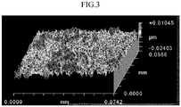
- FIG. 3 shows the three-dimensional data of the optical member according to the present disclosure, imaged by the non-contact type optical surface roughness tester
- FIG. 4 shows the image data of polishing marks in the optical member according to the present disclosure.
- the polishing marks as shown in FIG. 4 are easily formed by polishing the molded member in accordance with the production method to be described later.
- the polishing marks to be formed on the optical member according to the present disclosure are not limited to the shape, size and the like of those shown in FIG. 4 .
- the expression "height of linear marks” as used herein refers to the difference between the highest position and the lowest position of the linear marks imaged by the non-contact type optical surface roughness tester.
- At least some of the plurality of the linear marks may be parallel to one another, or may be crossed with one another.
- another layer such as an adhesive layer or a tacky layer
- another member is layered on the surface A, for example, the occurrence of relative positional displacement between the surface A and the other layer, or between the surface A and the other member, for example, can be more easily reduced.
- the region to be measured and observed by the non-contact type optical surface roughness tester may be a region having an area of 4,200 ⁇ m 2 whose center is the center of gravity of the surface A.
- another layer such as an adhesive layer or a tacky layer
- the presence of the linear marks enhances the adhesion between the surface A and the other layer, making the relative positional displacement between the surface A and the other layer less likely to occur.
- another member is provided so as to be in contact with the surface A, the relative positional displacement between the surface A and the other member is less likely to occur.
- the optical member according to the present disclosure preferably has a Vickers hardness at 23°C of 1 GPa or less. In other words, it is preferred that the optical member is relatively soft.
- the Vickers hardness at 23°C of the optical member may be measured in accordance with JIS Z 2244 (2009).
- the optical member according to the present disclosure preferably has a tensile elastic modulus at 23°C of from 1.0 ⁇ 10 3 MPa to 5.0 ⁇ 10 3 MPa.
- the tensile elastic modulus at 23°C of the optical member may be measured in accordance with JIS K 7161-1 (2014).
- a method of producing the optical member according to the present disclosure to be described later enables to obtain an optical member which satisfies at least one of the Vickers hardness at 23°C and the tensile elastic modulus at 23°C described above, and which has an excellent flatness of the surface A.
- the optical member may have a total light transmittance of 10% or more.
- the total light transmittance of the optical member may be measured in accordance with JIS K 7361-1 (1997).
- the optical member preferably has a haze (total haze) of 10% or less, more preferably 1% or less, and still more preferably 0.5% or less.
- the haze of the optical member as used herein refers to a value measured at 25°C in accordance with JIS-K 7105, using a haze meter [TC-HIII DPK; manufactured by Tokyo Denshoku Co., Ltd.].
- the shape of the optical member is not particularly limited, and may be in the form of a plate, a cylinder, a rectangular parallelopiped, or the like.
- the optical member has a shape with corners, such as a shape in the form of a plate or a rectangular parallelopiped, the force for forming the surface A is concentrated to the corners, during the formation of the surface A, making the parallelism or the flatness in the vicinity of the corners to be more likely to be impaired.
- the method of producing the optical member according to the present disclosure to be described later enables to form the surface A without applying an excessive force to the corners, during the formation of the surface A, making it possible to reduce the values of the parallelism, flatness and the like of the optical member.
- the optical member preferably has a refractive index of 1.58 or more.
- the optical member may have a refractive index of 1.80 or less, or 1.75 or less.
- the refractive index of the optical member may be measured in accordance with JIS K 7142 (2014).
- the optical member preferably includes, as the organic polymer to be included therein, at least one selected from the group consisting of a poly(thio)urethane resin, an episulfide resin, a polycarbonate resin, a polyester resin, a polyamide resin, a polyimide resin, a poly(meth)acrylate resin, a polyolefin resin, a polyurea-urethane resin, a polysulfide resin, a poly(meth)(thio)acrylate resin and an allyl diglycidyl carbonate resin.
- a poly(thio)urethane resin, an episulfide resin and a polycarbonate resin are preferred, and a poly(thio)urethane resin and an episulfide resin are more preferred, as the organic polymer, from the viewpoint of improving the refractive index.
- the poly(thio)urethane resin is preferably a thiourethane resin. More specifically, a thiourethane resin obtained by polymerizing a diisocyanate compound and a thiol compound is preferred.
- diisocyanate compound examples include 2,4-tolylene diisocyanate, 2,6-tolylene diisocyanate, diphenylmethane diisocyanate, m-xylylene diisocyanate, m-phenylene diisocyanate, isophorone diisocyanate, hexamethylene diisocyanate, 2,5-bis(isocyanatomethyl)bicyclo-[2.2.1]-heptane, 2,6-bis(isocyanatomethyl)bicyclo-[2.2.1]-heptane, 1,3-bis(isocyanatomethyl)cyclohexane, 1,4-bis(isocyanatomethyl)cyclohexane, bis(4-isocyanatocyclohexyl)methane, and 1,5-pentamethylene diisocyanate. These diisocyanate compounds may be used singly, or in combination of two or more kinds thereof.
- thiol compound examples include pentaerythritol tetrakis(3-mercaptopropionate), pentaerythritol tetrakis(2-mercaptoacetate), 4-mercaptomethyl-1,8-dimercapto-3,6-dithiaoctane, 5,7-dimercaptomethyl-1, 11-dimercapto-3,6,9-trithiaundecane, 4,7-dimercaptomethyl-1,11-dimercapto-3,6,9-trithiaundecane, 4,8-dimercaptomethyl-1,11-dimercapto-3,6,9-trithiaundecane, 2,5-dimercaptomethyl-1,4-dithiane, 1,1,3,3-tetrakis(mercaptomethylthio)propane, 4,6-bis(mercaptomethylthio)-1,3 -dithiane, 2-(2,2-bis(mercaptomethylthio)eth
- the episulfide resin may be any resin in which a compound having an episulfide group is used as a main component or a sub component of a starting material of the resin.
- Examples of the compound having an episulfide group include episulfide compounds described in in WO 2017/159839 and Japanese Patent Application Laid-Open ( JP-A) No. 2018-154690 , thioepoxy compounds described in JP-A No. 2002-194083 , and novel tetrathiaspiro compounds described in in JP-A No.2019-1785 .
- the content of the organic polymer included in the optical member is preferably 80% by mass or more, and more preferably 90% by mass or more, with respect to the total amount of the optical member, from the viewpoint achieving a reduction in weight. Further, the content of the organic polymer included in the optical member may be 100% by mass, or may be 99% by mass or less, with respect to the total amount of the optical member.
- the optical member may include another component other than the organic polymer.
- the other component include ultraviolet absorbers, antioxidants, photostabilizers, deterioration inhibitors, pigments (such as photochromic materials), release agents, dyes, pigments, and polymerization catalysts.
- the application of the optical member according to the present disclosure is not particularly limited, and can be used, for example, in a display device, an imaging apparatus, an optical device or the like. More specifically, the optical member can be used in a wearable device, still more specifically, in a wearable display in which virtual reality (VR), augmented reality (AR) or the like is realized.
- VR virtual reality
- AR augmented reality
- a method of producing the optical member according to the present disclosure includes:
- the production method includes a step of preparing a molded member including an organic polymer.
- the molded member is an optical member before being subjected to a polishing treatment, and the shape of the molded member may be selected as appropriate, depending on the shape of the optical member to be produced.
- the molded member may be produced by pouring a composition containing monomers as raw materials of the organic polymer into a mold, and then irradiating UV light or the like to the composition so as to polymerize the monomers.
- the production method includes the first polishing step of polishing the molded member with a polishing pad, after arranging the molded member in a movement restriction member which restricts the movement of the molded member during the polishing of the molded member.
- the first polishing step at least one surface of the molded member which will constitute the surface A in the resulting optical member is polished, and preferably, each of both surfaces of the molded member which will constitute the surface A and the surface B in the resulting optical member is polished.
- the polishing may be performed using a single-sided polishing machine in which a polishing pad is provided on one of the upper and lower lapping plates.
- the polishing may be performed using a double-sided polishing machine in which a polishing pad is provided on each of both the upper and lower lapping plates.
- the movement restriction member is required to have a configuration which allows the molded member to be arranged therein, and enables to restrict the movement of the molded member during the polishing of the molded member with a polishing pad.
- the movement restriction member may have a configuration which retains the molded member such that the molded member is not movable relative to the movement restriction member, during the polishing of the molded member with a polishing pad.
- the movement restriction member may have a configuration which allows the molded member to be arranged therein such that the molded member is movable relative to the movement restriction member. In the latter configuration, an optical member in which the flatness of the surface A is high, and which is excellent in the parallelism between the surface A and the surface B tends to be more easily obtained.
- the molded member may be polished while supplying a known polishing liquid, grinding liquid or the like.
- the molded member is preferably polished using an abrasive material having a grain size of from 5 ⁇ m to 10 ⁇ m, and more preferably using an abrasive material having a grain size of from 7 ⁇ m to 10 ⁇ m, from the viewpoint of improving the polishability of the molded member.
- the polishing of the molded member using the abrasive material having a grain size of 3 ⁇ m or more described above can be performed, for example, by: a method of polishing the molded member using a polishing pad (having a pad roughness of 3 ⁇ m or more) in which an abrasive material (fixed abrasive grains), such as diamond having a grain size of 3 ⁇ m or more, is embedded; or a method of polishing the molded member using an abrasive material (loose abrasive grains), such as diamond having a grain size of 3 ⁇ m or more, and a polishing pad.
- a polishing pad having a pad roughness of 3 ⁇ m or more
- an abrasive material fixed abrasive grains
- an abrasive material loose abrasive grains
- an abrasive material having a smaller grain size is more preferred, in order to smoothen the surface(s) of a molded member including an inorganic material.
- polishing a molded member including an organic polymer, which is softer than an inorganic material in contrast, the present inventors have found out that the values of the parallelism, flatness and the like can be reduced by using an abrasive material having a grain size equal to or higher than a certain value, different from the usual case.
- the molded member is preferably arranged in the movement restriction member such that the clearance between the molded member and the movement restriction member is 1 mm or more.
- the clearance described above is preferably 3 mm or more, more preferably 5 mm or more, and still more preferably 10 mm or more. Further, the clearance may be 30 mm or less.
- the term "clearance” refers to a value represented by (A-B)/2, wherein A and B are defined as follows.
- a and B are defined as follows.
- the maximum value of the distance between the side surfaces is defined as length A; in a case in which the movement restriction member has a side surface in the form of a circle, the diameter of the member is defined as the length A; in a case in which the molded member has side surfaces in the form of a polygon, the maximum value of the distance between the side surfaces is defined as length B; and in a case in which the molded member has a side surface in the form of a circle, the diameter of the member is defined as the length B.
- Providing a clearance enables to prevent an excessive force from being applied to the peripheral portion of the molded member including an organic polymer, during the polishing of the molded member including an organic polymer, making it possible to reduce the values of the parallelism, flatness and the like.
- providing a clearance makes the movement restriction member and the peripheral portion of the molded member more prone to collide with each other during the formation of the surface A, it is assumed that the molded member is less susceptible to deformation even when the movement restriction member and the peripheral portion of the molded member collide with each other during the formation of the surface A, because of the flexibility of the molded member including an organic polymer.
- the molded member may be polished by planetary polishing.
- planetary polishing refers to polishing the molded members while allowing the movement restriction members in which the molded members are arranged to revolve and rotate.
- FIG. 1 shows a perspective view illustrating the meshing relationship between a sun gear, an internal gear and movement restriction members, in a planetary gear system.
- the planetary gear system shown in FIG. 1 includes: a sun gear 30; an internal gear 40 arranged concentrically outside the sun gear 30; and movement restriction members 50 which mesh with the sun gear 30 and the internal gear 40, and which revolve and rotate corresponding to the rotation of the sun gear 30 and the internal gear 40.
- a plurality of molded members W are arranged in each of these movement restriction members 50. Further, both surfaces of the molded members W arranged in the movement restriction members 50 are polished by polishing pads which are provided on the upper and lower lapping plates of the double-sided polishing machine employing the planetary gear system.
- the speed of rotation of the upper polishing pad is preferably from 5 rpm to 30 rpm, and more preferably from 7 rpm to 20 rpm.
- the speed of rotation of the lower polishing pad is preferably from 20 rpm to 50 rpm, and more preferably from 25 rpm to 40 rpm.
- the direction of rotation of the upper polishing pad may be the same as, or the opposite of that of the lower polishing pad.
- the speed of revolution of the movement restriction members in which the molded members are arranged is preferably from 5 rpm to 30 rpm, and more preferably from 7 rpm to 20 rpm.
- the direction of revolution of the movement restriction members may be the same as, or the opposite of that of the lower polishing pad.
- the speed of rotation of the movement restriction members in which the molded members are arranged is preferably from 2 rpm to 50 rpm, and more preferably from 5 rpm to 20 rpm.
- the method of producing the optical member according to the present disclosure further includes a second polishing step of polishing the molded member after being subjected to the first polishing step, with a polishing pad and an abrasive material.
- a polishing pad different from one used in the first polishing step such as, for example, a suede type polishing pad in which a nap layer made of a resin such as a urethane resin or an ester resin is provided on a substrate.
- the molded member may be polished while supplying a known polishing liquid, grinding liquid or the like which contains an abrasive material such as alumina.
- An apparatus for transmitting optical information according to the present disclosure include:
- the above described optical members according to the present disclosure may be directly disposed one on another in layers, or may be disposed one on another in layers with an adhesive layer(s) interposed between the optical members.
- the adhesive layer may be formed, for example, by applying a composition containing monomers as raw materials of an organic polymer to one optical member, to form a composition layer, sandwiching the thus formed composition layer between two pieces of the optical members, and then irradiating light, such as UV light, to the composition layer so as to polymerize the monomers.
- FIG. 2 shows one example of the apparatus for transmitting optical information according to the present disclosure.
- An apparatus for transmitting optical information 10 includes: an image display section 1; and a light guide in which a plurality of optical members 2 are arranged. The light generated from the image display section 1 is reflected by the optical members 2 in the light guide, and the light reflected and scattered by the plurality of the optical members 2 is irradiated into the eyes of a user wearing the apparatus for transmitting optical information 10, as a result of which an image displayed on the image display section 1 is recognized by the user.
- molded members each composed of the following material, and is in the form of a disk having a diameter of 80 mm and a height of 1.7 mm, were prepared.
- the molded members had a Vickers hardness of 228 MPa, and a tensile elastic modulus at 23°C of 3.8 ⁇ 10 3 MPa.
- MR10 (a thiourethane resin; refractive index: 1.67; manufactured by Mitsui Chemicals, Inc.)
- the thus prepared molded members were arranged in fixing devices (corresponding to movement restriction members) with openings on both surfaces, of a polishing apparatus (9B double-sided lapping machine), such that the two circular surfaces of each molded member would be the surfaces to be polished.
- the clearance between wall surfaces of the fixing devices and the molded members was set to 20 mm.
- the first polishing step was carried out, using the polishing pads and the grinding liquid shown below, and under the following polishing conditions.
- the molded members were polished (by planetary polishing) by: introducing the grinding liquid under the following conditions; rotating the upper pad and the lower pad under the following conditions; and allowing the fixing devices in which the molded members were arranged to rotate and revolve under the following conditions.
- the second polishing step was carried out, using the polishing pads and the grinding liquid shown below, and under the following polishing conditions.
- the clearance between the wall surfaces of the fixing devices and the molded members was to 20 mm. (Polishing Pads (Upper Pad and Lower Pad))
- the molded members were polished (by planetary polishing) by: introducing the grinding liquid under the following conditions; rotating the upper pad and the lower pad under the following conditions; and allowing the fixing devices in which the molded members were arranged to rotate and revolve under the following conditions.
- the first polishing step and the second polishing step described above were performed to obtain optical members each in the form of a disk having a diameter of 80 mm and a height of 0.81 mm.
- molded members each composed of the following material, and is in the form of a disk having a diameter of 80 mm and a height of 2.0 mm, were prepared.
- the molded members had a Vickers hardness of 205 MPa, and a tensile elastic modulus at 23°C of 3.1 ⁇ 10 3 MPa.
- MR8 (a thiourethane resin; refractive index: 1.6; manufactured by Mitsui Chemicals, Inc.)
- the first polishing step was carried out in the same manner as in Experimental Examples 1 to 4, except that the clearance between the wall surfaces of the fixing devices and the molded members were changed from 20 mm to 0.5 mm, and the pad pressure was changed from a surface pressure of 80 g to 100 g.
- the polishing amount in the first polishing step was 1,170 ⁇ m.
- the second polishing step was carried out in the same manner as in Experimental Examples 1 to 4, except that the clearance between the wall surfaces of the fixing devices and the molded members were changed from 20 mm to 0.5 mm, the speed of rotation of the upper pad was changed from 10 rpm to 5 rpm, the speed of rotation of the lower pad was changed from 30 rpm to 15 rpm, the speed of rotation of the fixing devices was changed from 5 rpm to 2 rpm, and the speed of revolution of the fixing devices was changed from 10 rpm to 5 rpm.
- the polishing amount in the second polishing step was 22 ⁇ m.
- the first polishing step and the second polishing step described above were performed to obtain optical members each in the form of a disk having a diameter of 80 mm and a height of 0.808 mm.
- the first polishing step was carried out in the same manner as in Experimental Examples 1 to 4, except that the diamond pads (pad roughness: 9 ⁇ m, corresponding to #2000) used in Experimental Examples 1 to 4 were changed to diamond pads (pad roughness: 2 ⁇ m, corresponding to #6000). However, the polishing of the molded members did not proceed in Experimental Example 8.
- the first polishing step was carried out in the same manner as in Experimental Examples 5 to 7, except that the diamond pads (pad roughness: 9 ⁇ m, corresponding to #2000) used in Experimental Examples 5 to 7 were changed to diamond pads (pad roughness: 2 ⁇ m, corresponding to #6000). However, the polishing of the molded members did not proceed in Experimental Example 9.
Landscapes
- Physics & Mathematics (AREA)
- General Physics & Mathematics (AREA)
- Optics & Photonics (AREA)
- Engineering & Computer Science (AREA)
- Mechanical Engineering (AREA)
- Finish Polishing, Edge Sharpening, And Grinding By Specific Grinding Devices (AREA)
- Optical Elements Other Than Lenses (AREA)
Abstract
Description
- The present disclosure relates to an optical member, a method of producing the optical member, and an apparatus for transmitting optical information.
- In recent years, requirements on flatness, surface defects and the like of glass substrates for electronic devices are getting stricter. For example, glass substrates for electronic devices, such as glass substrates for mask blanks, which have a high flatness and less microdefects (such as recess defects and protrusion defects) are demanded. As a method for producing such glass substrates for mask blanks which have a high flatness and less microdefects (such as recess defects and protrusion defects), a method has been investigated in which: a plurality of glass substrates are sandwiched between an upper lapping plate and a lower lapping plate that are disposed so as to face each other in the vertical direction and each provided with a polishing pad; and both main surfaces of the glass substrates are polished, while supplying a polishing liquid to the glass substrates from the side of the upper lapping plate (see
Patent Document 1, for example). - Patent Document 1: Japanese Patent Publication (
JP-B) No. 6002528 - Optical members are desired to be capable of transmitting light with a high accuracy, and inorganic materials such as glass have been used, because of ease of production by polishing and the like. In recent years, however, reduction in weight is required for optical members for use in wearable devices, for example, and attempts have been made to achieve a reduction in weight by reducing the thickness of optical members made of inorganic materials.
- It is common technical knowledge that, although a further reduction in weight can be expected by using organic materials instead, as materials for optical members, it causes problems, for example, that optical members become more susceptible to deformation and damage when processing organic materials into optical members. Accordingly, optical members produced using organic materials are difficult to achieve a highly accurate transmission of optical information, and attempts to use organic materials for optical members are extremely rare.
- The present disclosure has been made in view of the problems described above, and an object of the present disclosure is to provide an optical member which is lightweight and is capable of transmitting optical information with a high accuracy, a method of producing the same, and an apparatus for transmitting optical information including the optical member.
- The present disclosure relates to the following embodiments.
- <1> An optical member comprising an organic polymer,
wherein the optical member comprises a surface A which has an area of 1 mm2 or more, and in which a flatness of a region having an area of 1 mm2, as measured by a non-contact type optical flatness meter, is 80 µm or less. - <2> The optical member according to <1>, wherein the flatness of the surface A is 50 µm or less.
- <3> The optical member according to <1> or <2> comprising a surface B located on an opposite side of the surface A, and having an area of 1 mm2 or more,
wherein, when a flatness of a region having an area of 1 mm2 is measured for each of the surface A and the surface B by the non-contact type optical flatness meter, an absolute value of a difference between the flatness of the surface A and the flatness of the surface B is 5 µm or less. - <4> An optical member comprising an organic polymer,
- wherein the optical member comprises:
- a surface A having an area of 1 mm2 or more; and
- a surface B located on an opposite side of the surface A, and having an area of 1 mm2 or more; and
- wherein, when a flatness of a region having an area of 1 mm2 is measured for each of the surface A and the surface B by a non-contact type optical flatness meter, an absolute value of a difference between the flatness of the surface A and the flatness of the surface B is 5 µm or less.
- wherein the optical member comprises:
- <5> The optical member according to <3> or <4>, wherein an average distance between the surface A and the surface B is 10 mm or less.
- <6> The optical member according to any one of <1> to <5>, wherein an arithmetic average roughness Ra of a region having an area of 4,200 µm2 in the surface A, as measured by a non-contact type optical surface roughness tester, is 10 nm or less.
- <7> The optical member according to any one of <1> to <6>, wherein the optical member has a refractive index of 1.58 or more.
- <8> The optical member according to any one of <1> to <7>, wherein, a plurality of linear marks having a height of 50 nm or less are observed, in an image of a region having an area of 4,200 µm2 in the surface A, when the region is imaged by a non-contact type optical surface roughness tester.
- <9> The optical member according to any one of <1> to <8>, wherein the optical member has a Vickers hardness at 23°C of 1 GPa or less.
- <10> The optical member according to any one of <1> to <9>, wherein the optical member has a tensile elastic modulus at 23°C of from 1.0 × 10³ MPa to 5.0 × 10³ MPa.
- <11> The optical member according to any one of <1> to <10>, wherein the organic polymer comprises at least one selected from the group consisting of a poly(thio)urethane resin, an episulfide resin, a polycarbonate resin, a polyester resin, a polyamide resin, a polyimide resin, a poly(meth)acrylate resin, a polyolefin resin, a polyurea-urethane resin, a polysulfide resin, a poly(meth)(thio)acrylate resin and an allyl diglycidyl carbonate resin.
- <12> The optical member according to any one of <1> to <11>, wherein the optical member is for use in a wearable device.
- <13> A method of producing the optical member according to any one of <1> to <12>, the method comprising:
- a step of preparing a molded member including an organic polymer; and
- a first polishing step of polishing the molded member with a polishing pad, after arranging the molded member in a movement restriction member which restricts the movement of the molded member during the polishing of the molded member,
- wherein, in the first polishing step, the molded member is polished using an abrasive material having a grain size of 3 µm or more.
- <14> The method of producing the optical member according to <13>, wherein the molded member is movable relative to the movement restriction member, during the polishing of the molded member with the polishing pad.
- <15> The method of producing the optical member according to <13> or <14>, wherein, in the first polishing step, the molded member is arranged in the movement restriction member such that a clearance between the molded member and the movement restriction member is 1 mm or more.
- <16> The method of producing the optical member according to any one of <13> to <15>, further comprising a second polishing step of polishing the molded member after being subjected to the first polishing step, with a polishing pad and an abrasive material.
- <17> An apparatus for transmitting optical information, the apparatus comprising:
- a light irradiation section; and
- a light guide comprising a plurality of the optical members according to any one of
claims 1 to 12, wherein the plurality of the optical members are arranged such that principal surfaces of the optical members are substantially parallel to one another.
- The present disclosure enables to provide an optical member which is lightweight and is capable of transmitting optical information with a high accuracy, a method of producing the same, and an apparatus for transmitting optical information including the optical member.
-
-
FIG. 1 is a perspective view showing a meshing relationship between a sun gear, an internal gear and movement restriction members, in a planetary gear system. -
FIG. 2 is a schematic configuration diagram showing one example of an apparatus for transmitting optical information according to the present disclosure. -
FIG. 3 shows three-dimensional data imaged by a non-contact type optical surface roughness tester. -
FIG. 4 shows image data of polishing marks. - Examples of preferred embodiments of the present disclosure will now be described in detail. The following descriptions and Examples are for illustrating the embodiments, and are not intended to limit the scope of the embodiments.
- In the present disclosure, any numerical range described using the expression "from ∗ to" represents a range in which numerical values described before and after the "to" are included in the range as a lower limit value and an upper limit value, respectively.
- In the present disclosure, the definition of the term "step" includes not only an independent step, but also a step which is not clearly distinguishable from another step, as long as the purpose of the step is achieved.
- In the present disclosure, the term "optical member" refers to a member composed of at least one layer including an organic polymer. An optical member according to the present disclosure may be in the form of a laminated body in which a plurality of members including an organic polymer are disposed one on another in layers, or may be in the form of a laminated body in which a member(s) including an organic polymer is/are layered with another member(s).
- An optical member according to the present disclosure includes an organic polymer, and includes a surface A which has an area of 1 mm2 or more, and in which the flatness of a region having an area of 1 mm2, as measured by a non-contact type optical flatness meter, is 80 µm or less. The optical member according to the present disclosure is lightweight due to including an organic polymer, and is capable of transmitting optical information with a high accuracy due to including the surface A in which the flatness is 80 µm or less.
- The position of the surface A in the optical member according to the present disclosure is not particularly limited. However, a configuration is preferred, in which the surface A is located on at least a part of the exposed surfaces (including a principal surface) of the optical member, because a high flatness of the surface A facilitates the transmission of optical information. In a case in which the surface A is located on a part of the exposed surfaces of the optical member according to the present disclosure, it is preferred that the surface A is located at a position at which the optical information to be transmitted by the surface A can be easily received. Specifically, the surface A is preferably located on the principal surface of the optical member, and further, in a region including the center of gravity of the principal surface is preferred.
- The region to be measured by the non-contact type optical flatness meter is not particularly limited, as long as the region is a region in the surface A which has an area of 1 mm2. Accordingly, the surface A in the optical member according to the present disclosure is required to include a region having an area of 1 mm2 in which the flatness is 80 µm or less, and the flatness of the region other than that region in the surface A may be 80 µm or less, or more than 80 µm. The entire surface A may have a flatness of 80 µm or less, or alternatively, 10% or more of the total area of the surface A, preferably 50% or more of the total area of the surface A may have a flatness of 80 µm or less.
- The region to be measured by the non-contact type optical flatness meter may be a region having an area of 1 mm2 whose center is the center of gravity of the surface A.
- The surface A is required to have a flatness of 80 µm or less, and is preferably 50 µm or less, more preferably 30 µm or less, still more preferably 20 µm or less, and particularly preferably 15 µm or less, from the viewpoint of improving the transmission of optical information.
- The lower limit of the flatness of the surface A is not particularly limited as long as the flatness is 0 µm or more, and may be 1 µm or more, or 5 µm or more.
- The area of the surface A is required to be 1 mm2 or more, and can be selected as appropriate, depending on the application of the optical member. For example, the area of the surface A may be within the range of from 10 mm2 to 20,000 mm2, or from 100 mm2 to 1,000 mm2.
- The optical member according to the present disclosure may include a surface B located on the opposite side of the surface A, and having an area of 1 mm2 or more.
- The preferred range of the area of the surface B is the same as the preferred range of the area of the surface A described above. Further, the areas of the surface A and the surface B area may be the same as, or different from, each other.
- In the surface B, the flatness of a region having an area of 1 mm2, as measured by the non-contact type optical flatness meter, may be 80 µm or less. The preferred range of the flatness of the surface B is the same as the preferred range of the flatness of the surface A described above.
- In the optical member according to the present disclosure, when the flatness of a region having an area of 1 mm2 is measured for each of the surface A and the surface B by the non-contact type optical flatness meter, the absolute value (hereinafter, also referred to as "parallelism") of the difference between the flatness of the surface A and the flatness of the surface B is preferably 5 µm or less. This configuration allows the optical member according to the present disclosure to transmit optical information with a high accuracy. For example, in a case in which a plurality of the optical members according to the present disclosure are layered such that the regions between which the parallelism is 5 µm or less are in contact with each other, to be formed into a laminated structure, the laminated structure enables to achieve the transmission of optical information with a high accuracy.
- The parallelism as described above is more preferably 4 µm or less, and still more preferably 3 µm or less. The lower limit of the parallelism is not particularly limited as long as the parallelism is 0 µm or more, and may be 0.5 µm or more, or 1.0 µm or more.
- The average distance between the surface A and the surface B may be 10 mm or less, 8 mm or less, or 6 mm or less. Further, the average distance between the surface A and the surface B may be 2 mm or more, or 4 mm or more.
- In the present disclosure, the expression "average distance between the surface A and the surface B" refers to a value obtained by dividing the sum of the maximum value of the distance between the surface A and the surface B, and the minimum value of the distance between the surface A and the surface B, by 2.
- In the optical member according to the present disclosure, the arithmetic average roughness Ra of a region having an area of 4,200 µm2 in the surface A, as measured by a non-contact type optical surface roughness tester, is preferably 10 nm or less, and more preferably 5 nm or less. The above described arithmetic average roughness Ra in the surface A may be more than 0.1 nm. The arithmetic average roughness Ra in the present disclosure is based on that defined in JIS B0601 (2013).
- The region to be measured by the non-contact type optical surface roughness tester is not particularly limited, as long as the region is that in the surface A which has an area of 4,200 µm2. Accordingly, the surface A in the optical member according to the present disclosure is required to include a region having an area of 4,200 µm2 in which the arithmetic average roughness Ra is 10 nm or less, and the arithmetic average roughness Ra of the region other than that region in the surface A may be 10 nm or less, or more than 10 nm.
- In the optical member according to the present disclosure, it is preferred that a plurality of linear marks having a height of 50 nm or less are observed, in an image of a region having an area of 4,200 µm2 in the surface A, when the region is imaged by a non-contact type optical surface roughness tester. By this configuration, in a case in which a plurality of the optical members according to the present disclosure are layered such that the regions in which the linear marks are observed are in contact with each other, for example, the resulting laminated structure can be more easily maintained. The plurality of the linear marks described above may be polishing marks, and may be polishing marks formed by polishing a molded member by a production method to be described later. Each as one example,
FIG. 3 shows the three-dimensional data of the optical member according to the present disclosure, imaged by the non-contact type optical surface roughness tester, andFIG. 4 shows the image data of polishing marks in the optical member according to the present disclosure. The polishing marks as shown inFIG. 4 are easily formed by polishing the molded member in accordance with the production method to be described later. The polishing marks to be formed on the optical member according to the present disclosure are not limited to the shape, size and the like of those shown inFIG. 4 . - The expression "height of linear marks" as used herein refers to the difference between the highest position and the lowest position of the linear marks imaged by the non-contact type optical surface roughness tester.
- From the viewpoint of maintaining the laminated structure of the optical members, it is preferred that five or more of the linear marks described above are observed, in an image of a region having an area of 4,200 µm2 in the surface A, when the region is imaged by the non-contact type optical surface roughness tester.
- At least some of the plurality of the linear marks may be parallel to one another, or may be crossed with one another. In particular, when at least some of the plurality of the linear marks are crossed with one another, and in a case in which another layer (such as an adhesive layer or a tacky layer) is layered on the surface A, or another member is layered on the surface A, for example, the occurrence of relative positional displacement between the surface A and the other layer, or between the surface A and the other member, for example, can be more easily reduced.
- The region to be measured and observed by the non-contact type optical surface roughness tester may be a region having an area of 4,200 µm2 whose center is the center of gravity of the surface A. In a case in which another layer (such as an adhesive layer or a tacky layer) is layered on the surface A, the presence of the linear marks enhances the adhesion between the surface A and the other layer, making the relative positional displacement between the surface A and the other layer less likely to occur. Further, in a case in which another member is provided so as to be in contact with the surface A, the relative positional displacement between the surface A and the other member is less likely to occur.
- The optical member according to the present disclosure preferably has a Vickers hardness at 23°C of 1 GPa or less. In other words, it is preferred that the optical member is relatively soft. The Vickers hardness at 23°C of the optical member may be measured in accordance with JIS Z 2244 (2009).
- The optical member according to the present disclosure preferably has a tensile elastic modulus at 23°C of from 1.0 × 10³ MPa to 5.0 × 10³ MPa. The tensile elastic modulus at 23°C of the optical member may be measured in accordance with JIS K 7161-1 (2014).
- For example, a method of producing the optical member according to the present disclosure to be described later enables to obtain an optical member which satisfies at least one of the Vickers hardness at 23°C and the tensile elastic modulus at 23°C described above, and which has an excellent flatness of the surface A.
- The optical member may have a total light transmittance of 10% or more. The total light transmittance of the optical member may be measured in accordance with JIS K 7361-1 (1997).
- The optical member preferably has a haze (total haze) of 10% or less, more preferably 1% or less, and still more preferably 0.5% or less. The haze of the optical member as used herein refers to a value measured at 25°C in accordance with JIS-K 7105, using a haze meter [TC-HIII DPK; manufactured by Tokyo Denshoku Co., Ltd.].
- The shape of the optical member is not particularly limited, and may be in the form of a plate, a cylinder, a rectangular parallelopiped, or the like. In the case of adjusting the shape of the optical member by processing, it is preferred to perform the processing of the optical member before forming the surface A of the optical member, because the parallelism, flatness and the like of the surface A are more likely to be impaired when the processing of the optical member is performed after the formation of the surface A. In general, when the optical member has a shape with corners, such as a shape in the form of a plate or a rectangular parallelopiped, the force for forming the surface A is concentrated to the corners, during the formation of the surface A, making the parallelism or the flatness in the vicinity of the corners to be more likely to be impaired. In contrast, the method of producing the optical member according to the present disclosure to be described later enables to form the surface A without applying an excessive force to the corners, during the formation of the surface A, making it possible to reduce the values of the parallelism, flatness and the like of the optical member.
- The optical member preferably has a refractive index of 1.58 or more. The optical member may have a refractive index of 1.80 or less, or 1.75 or less. The refractive index of the optical member may be measured in accordance with JIS K 7142 (2014).
- The optical member preferably includes, as the organic polymer to be included therein, at least one selected from the group consisting of a poly(thio)urethane resin, an episulfide resin, a polycarbonate resin, a polyester resin, a polyamide resin, a polyimide resin, a poly(meth)acrylate resin, a polyolefin resin, a polyurea-urethane resin, a polysulfide resin, a poly(meth)(thio)acrylate resin and an allyl diglycidyl carbonate resin. Among these resins, a poly(thio)urethane resin, an episulfide resin and a polycarbonate resin are preferred, and a poly(thio)urethane resin and an episulfide resin are more preferred, as the organic polymer, from the viewpoint of improving the refractive index.
- The poly(thio)urethane resin is preferably a thiourethane resin. More specifically, a thiourethane resin obtained by polymerizing a diisocyanate compound and a thiol compound is preferred.
- Examples of the diisocyanate compound include 2,4-tolylene diisocyanate, 2,6-tolylene diisocyanate, diphenylmethane diisocyanate, m-xylylene diisocyanate, m-phenylene diisocyanate, isophorone diisocyanate, hexamethylene diisocyanate, 2,5-bis(isocyanatomethyl)bicyclo-[2.2.1]-heptane, 2,6-bis(isocyanatomethyl)bicyclo-[2.2.1]-heptane, 1,3-bis(isocyanatomethyl)cyclohexane, 1,4-bis(isocyanatomethyl)cyclohexane, bis(4-isocyanatocyclohexyl)methane, and 1,5-pentamethylene diisocyanate. These diisocyanate compounds may be used singly, or in combination of two or more kinds thereof.
- Examples of the thiol compound include pentaerythritol tetrakis(3-mercaptopropionate), pentaerythritol tetrakis(2-mercaptoacetate), 4-mercaptomethyl-1,8-dimercapto-3,6-dithiaoctane, 5,7-dimercaptomethyl-1, 11-dimercapto-3,6,9-trithiaundecane, 4,7-dimercaptomethyl-1,11-dimercapto-3,6,9-trithiaundecane, 4,8-dimercaptomethyl-1,11-dimercapto-3,6,9-trithiaundecane, 2,5-dimercaptomethyl-1,4-dithiane, 1,1,3,3-tetrakis(mercaptomethylthio)propane, 4,6-bis(mercaptomethylthio)-1,3 -dithiane, 2-(2,2-bis(mercaptomethylthio)ethyl)-1,3-dithietane, 1,2-bis(mercaptomethyl)benzene, 1,3-bis(mercaptomethyl)benzene, and 1,4-bis(mercaptomethyl)benzene. These thiol compounds may be used singly, or in combination of two or more kinds thereof.
- The episulfide resin may be any resin in which a compound having an episulfide group is used as a main component or a sub component of a starting material of the resin. Examples of the compound having an episulfide group include episulfide compounds described in in
WO 2017/159839 and Japanese Patent Application Laid-Open (JP-A) No. 2018-154690 JP-A No. 2002-194083 JP-A No.2019-1785 - The content of the organic polymer included in the optical member is preferably 80% by mass or more, and more preferably 90% by mass or more, with respect to the total amount of the optical member, from the viewpoint achieving a reduction in weight. Further, the content of the organic polymer included in the optical member may be 100% by mass, or may be 99% by mass or less, with respect to the total amount of the optical member.
- The optical member may include another component other than the organic polymer. Examples of the other component include ultraviolet absorbers, antioxidants, photostabilizers, deterioration inhibitors, pigments (such as photochromic materials), release agents, dyes, pigments, and polymerization catalysts.
- The application of the optical member according to the present disclosure is not particularly limited, and can be used, for example, in a display device, an imaging apparatus, an optical device or the like. More specifically, the optical member can be used in a wearable device, still more specifically, in a wearable display in which virtual reality (VR), augmented reality (AR) or the like is realized.
- A method of producing the optical member according to the present disclosure includes:
- a step of preparing a molded member including an organic polymer; and
- a first polishing step of polishing the molded member with a polishing pad, after arranging the molded member in a movement restriction member which restricts the movement of the molded member during the polishing of the molded member;
- wherein, in the first polishing step, the molded member is polished using an abrasive material having a grain size of 3 µm or more.
- The production method according to the present disclosure includes a step of preparing a molded member including an organic polymer. The molded member is an optical member before being subjected to a polishing treatment, and the shape of the molded member may be selected as appropriate, depending on the shape of the optical member to be produced. For example, the molded member may be produced by pouring a composition containing monomers as raw materials of the organic polymer into a mold, and then irradiating UV light or the like to the composition so as to polymerize the monomers.
- The production method according to the present disclosure includes the first polishing step of polishing the molded member with a polishing pad, after arranging the molded member in a movement restriction member which restricts the movement of the molded member during the polishing of the molded member. In the first polishing step, at least one surface of the molded member which will constitute the surface A in the resulting optical member is polished, and preferably, each of both surfaces of the molded member which will constitute the surface A and the surface B in the resulting optical member is polished. In the case of polishing one surface of the molded member, the polishing may be performed using a single-sided polishing machine in which a polishing pad is provided on one of the upper and lower lapping plates. In the case of polishing both surfaces of the molded member, the polishing may be performed using a double-sided polishing machine in which a polishing pad is provided on each of both the upper and lower lapping plates.
- The movement restriction member is required to have a configuration which allows the molded member to be arranged therein, and enables to restrict the movement of the molded member during the polishing of the molded member with a polishing pad. Further, the movement restriction member may have a configuration which retains the molded member such that the molded member is not movable relative to the movement restriction member, during the polishing of the molded member with a polishing pad. Alternatively, the movement restriction member may have a configuration which allows the molded member to be arranged therein such that the molded member is movable relative to the movement restriction member. In the latter configuration, an optical member in which the flatness of the surface A is high, and which is excellent in the parallelism between the surface A and the surface B tends to be more easily obtained.
- In the first polishing step, the molded member may be polished while supplying a known polishing liquid, grinding liquid or the like.
- In the first polishing step, the molded member is preferably polished using an abrasive material having a grain size of from 5 µm to 10 µm, and more preferably using an abrasive material having a grain size of from 7 µm to 10 µm, from the viewpoint of improving the polishability of the molded member. The polishing of the molded member using the abrasive material having a grain size of 3 µm or more described above, can be performed, for example, by: a method of polishing the molded member using a polishing pad (having a pad roughness of 3 µm or more) in which an abrasive material (fixed abrasive grains), such as diamond having a grain size of 3 µm or more, is embedded; or a method of polishing the molded member using an abrasive material (loose abrasive grains), such as diamond having a grain size of 3 µm or more, and a polishing pad. In general, an abrasive material having a smaller grain size is more preferred, in order to smoothen the surface(s) of a molded member including an inorganic material. In the case of polishing a molded member including an organic polymer, which is softer than an inorganic material, in contrast, the present inventors have found out that the values of the parallelism, flatness and the like can be reduced by using an abrasive material having a grain size equal to or higher than a certain value, different from the usual case.
- In the first polishing step, the molded member is preferably arranged in the movement restriction member such that the clearance between the molded member and the movement restriction member is 1 mm or more. By this configuration, an optical member which has a higher flatness of the surface A, and which has a better parallelism between the surface A and the surface B tends to be more easily obtained.
- In the first polishing step, the clearance described above is preferably 3 mm or more, more preferably 5 mm or more, and still more preferably 10 mm or more. Further, the clearance may be 30 mm or less.
- In the present disclosure, the term "clearance" refers to a value represented by (A-B)/2, wherein A and B are defined as follows. In a case in which the movement restriction member has side surfaces in the form of a polygon, the maximum value of the distance between the side surfaces is defined as length A; in a case in which the movement restriction member has a side surface in the form of a circle, the diameter of the member is defined as the length A; in a case in which the molded member has side surfaces in the form of a polygon, the maximum value of the distance between the side surfaces is defined as length B; and in a case in which the molded member has a side surface in the form of a circle, the diameter of the member is defined as the length B. Providing a clearance enables to prevent an excessive force from being applied to the peripheral portion of the molded member including an organic polymer, during the polishing of the molded member including an organic polymer, making it possible to reduce the values of the parallelism, flatness and the like. Although providing a clearance makes the movement restriction member and the peripheral portion of the molded member more prone to collide with each other during the formation of the surface A, it is assumed that the molded member is less susceptible to deformation even when the movement restriction member and the peripheral portion of the molded member collide with each other during the formation of the surface A, because of the flexibility of the molded member including an organic polymer. In contrast, in a case in which an inorganic-based molded member, which includes a hard inorganic material such as glass as a main component, is polished with a clearance provided, it is thought that the force applied from the movement restriction member to the inorganic-based molded member is more easily transmitted to the entire portion of the inorganic-based molded member, making it possible to reduce the values of the parallelism, flatness and the like. However, it is expected that the movement restriction member and the peripheral portion of the inorganic-based molded member collide with each other, making the inorganic-based molded member more susceptible to damage.
- In the first polishing step, the molded member may be polished by planetary polishing. The term "planetary polishing" refers to polishing the molded members while allowing the movement restriction members in which the molded members are arranged to revolve and rotate.
- In the case of performing the planetary polishing of the molded members, it is preferred to use a double-sided polishing machine employing a planetary gear system.
FIG. 1 shows a perspective view illustrating the meshing relationship between a sun gear, an internal gear and movement restriction members, in a planetary gear system. The planetary gear system shown inFIG. 1 includes: asun gear 30; aninternal gear 40 arranged concentrically outside thesun gear 30; andmovement restriction members 50 which mesh with thesun gear 30 and theinternal gear 40, and which revolve and rotate corresponding to the rotation of thesun gear 30 and theinternal gear 40. In each of thesemovement restriction members 50, a plurality of molded members W are arranged. Further, both surfaces of the molded members W arranged in themovement restriction members 50 are polished by polishing pads which are provided on the upper and lower lapping plates of the double-sided polishing machine employing the planetary gear system. - In the case of using the double-sided polishing machine, the speed of rotation of the upper polishing pad is preferably from 5 rpm to 30 rpm, and more preferably from 7 rpm to 20 rpm. The speed of rotation of the lower polishing pad is preferably from 20 rpm to 50 rpm, and more preferably from 25 rpm to 40 rpm. The direction of rotation of the upper polishing pad may be the same as, or the opposite of that of the lower polishing pad.
- The speed of revolution of the movement restriction members in which the molded members are arranged is preferably from 5 rpm to 30 rpm, and more preferably from 7 rpm to 20 rpm. The direction of revolution of the movement restriction members may be the same as, or the opposite of that of the lower polishing pad.
- Further, the speed of rotation of the movement restriction members in which the molded members are arranged is preferably from 2 rpm to 50 rpm, and more preferably from 5 rpm to 20 rpm.
- It is preferred that the method of producing the optical member according to the present disclosure further includes a second polishing step of polishing the molded member after being subjected to the first polishing step, with a polishing pad and an abrasive material. In the second polishing step, it is possible to use a polishing pad different from one used in the first polishing step, such as, for example, a suede type polishing pad in which a nap layer made of a resin such as a urethane resin or an ester resin is provided on a substrate.
- In the second polishing step, the molded member may be polished while supplying a known polishing liquid, grinding liquid or the like which contains an abrasive material such as alumina.
- An apparatus for transmitting optical information according to the present disclosure include:
- a light irradiation section; and
- a light guide including a plurality of the optical members according to the present disclosure described above, wherein the plurality of the optical members are arranged such that principal surfaces of the optical members are substantially parallel to one another.
- In the apparatus for transmitting optical information according to the present disclosure, the above described optical members according to the present disclosure may be directly disposed one on another in layers, or may be disposed one on another in layers with an adhesive layer(s) interposed between the optical members. The adhesive layer may be formed, for example, by applying a composition containing monomers as raw materials of an organic polymer to one optical member, to form a composition layer, sandwiching the thus formed composition layer between two pieces of the optical members, and then irradiating light, such as UV light, to the composition layer so as to polymerize the monomers.
-
FIG. 2 shows one example of the apparatus for transmitting optical information according to the present disclosure. An apparatus for transmittingoptical information 10 includes: animage display section 1; and a light guide in which a plurality ofoptical members 2 are arranged. The light generated from theimage display section 1 is reflected by theoptical members 2 in the light guide, and the light reflected and scattered by the plurality of theoptical members 2 is irradiated into the eyes of a user wearing the apparatus for transmittingoptical information 10, as a result of which an image displayed on theimage display section 1 is recognized by the user. - The present invention will now be specifically described in further detail, based on Examples. However, it is noted that the invention is in no way limited to these Examples.
- First, molded members each composed of the following material, and is in the form of a disk having a diameter of 80 mm and a height of 1.7 mm, were prepared. The molded members had a Vickers hardness of 228 MPa, and a tensile elastic modulus at 23°C of 3.8 × 10³ MPa.
- MR10 (a thiourethane resin; refractive index: 1.67; manufactured by Mitsui Chemicals, Inc.)
- The thus prepared molded members were arranged in fixing devices (corresponding to movement restriction members) with openings on both surfaces, of a polishing apparatus (9B double-sided lapping machine), such that the two circular surfaces of each molded member would be the surfaces to be polished. The clearance between wall surfaces of the fixing devices and the molded members was set to 20 mm. Thereafter, the first polishing step was carried out, using the polishing pads and the grinding liquid shown below, and under the following polishing conditions.
-
- Diamond pads (pad roughness: 9 µm, corresponding to #2000)
(Grinding Liquid) - Grinding liquid (pH: 9.3)
(Polishing Conditions in First Polishing Step) - The molded members were polished (by planetary polishing) by: introducing the grinding liquid under the following conditions; rotating the upper pad and the lower pad under the following conditions; and allowing the fixing devices in which the molded members were arranged to rotate and revolve under the following conditions.
- The amount of the grinding liquid introduced: 3.8 L/min
- Pad pressure: surface pressure 80 g
- Speed of rotation of upper pad: 10 rpm (rotated in the direction opposite from that of the lower pad)
- Speed of rotation of lower pad: 30 rpm
- Speed of rotation of fixing devices: 5 rpm
- Speed of revolution of fixing devices: 10 rpm (rotated in the same direction as that of the lower pad)
- Polishing amount: 840 µm
- After performing the first polishing step described above, the second polishing step was carried out, using the polishing pads and the grinding liquid shown below, and under the following polishing conditions. The clearance between the wall surfaces of the fixing devices and the molded members was to 20 mm.
(Polishing Pads (Upper Pad and Lower Pad)) - Suede pads (thickness: 0.95 mm, compression rate: 3.5%)
- Nap layers (NAP length: 570 µm, compressive elastic modulus: 60%, opening diameter: 25 µm)
(Grinding Liquid) - POLIPLA 608S (high-purity alumina; average particle size: 1.3 µm, pH: 3.4; manufactured by Fujimi Incorporated)
(Polishing Conditions in Second Polishing Step) - The molded members were polished (by planetary polishing) by: introducing the grinding liquid under the following conditions; rotating the upper pad and the lower pad under the following conditions; and allowing the fixing devices in which the molded members were arranged to rotate and revolve under the following conditions.
- The amount of the grinding liquid introduced: 14 L/min
- Pad pressure: surface pressure 120 g
- Speed of rotation of upper pad: 10 rpm
- Speed of rotation of lower pad: 30 rpm
- Speed of rotation of fixing devices: 5 rpm
- Speed of revolution of fixing devices: 10 rpm
- Polishing amount: 49 µm
- The first polishing step and the second polishing step described above were performed to obtain optical members each in the form of a disk having a diameter of 80 mm and a height of 0.81 mm.
- First, molded members each composed of the following material, and is in the form of a disk having a diameter of 80 mm and a height of 2.0 mm, were prepared. The molded members had a Vickers hardness of 205 MPa, and a tensile elastic modulus at 23°C of 3.1 × 10³ MPa.
- MR8 (a thiourethane resin; refractive index: 1.6; manufactured by Mitsui Chemicals, Inc.)
- The first polishing step was carried out in the same manner as in Experimental Examples 1 to 4, except that the clearance between the wall surfaces of the fixing devices and the molded members were changed from 20 mm to 0.5 mm, and the pad pressure was changed from a surface pressure of 80 g to 100 g. The polishing amount in the first polishing step was 1,170 µm.
- Further, the second polishing step was carried out in the same manner as in Experimental Examples 1 to 4, except that the clearance between the wall surfaces of the fixing devices and the molded members were changed from 20 mm to 0.5 mm, the speed of rotation of the upper pad was changed from 10 rpm to 5 rpm, the speed of rotation of the lower pad was changed from 30 rpm to 15 rpm, the speed of rotation of the fixing devices was changed from 5 rpm to 2 rpm, and the speed of revolution of the fixing devices was changed from 10 rpm to 5 rpm. The polishing amount in the second polishing step was 22 µm.
- The first polishing step and the second polishing step described above were performed to obtain optical members each in the form of a disk having a diameter of 80 mm and a height of 0.808 mm.
- The first polishing step was carried out in the same manner as in Experimental Examples 1 to 4, except that the diamond pads (pad roughness: 9 µm, corresponding to #2000) used in Experimental Examples 1 to 4 were changed to diamond pads (pad roughness: 2 µm, corresponding to #6000). However, the polishing of the molded members did not proceed in Experimental Example 8.
- The first polishing step was carried out in the same manner as in Experimental Examples 5 to 7, except that the diamond pads (pad roughness: 9 µm, corresponding to #2000) used in Experimental Examples 5 to 7 were changed to diamond pads (pad roughness: 2 µm, corresponding to #6000). However, the polishing of the molded members did not proceed in Experimental Example 9.
- For each of the two circular surfaces of each of the optical members of Experimental Examples 1 to 7, the flatness of the region having an area of 1 mm2 whose center is the center of gravity was measured, using a flatness measurement device (FlatMaster-Industrial, manufactured by Corning Tropel). Further, the absolute value of the difference in flatness between the two circular surfaces measured, was calculated.
- The results are shown in Table 1.
- For each of the two circular surfaces of each of the optical members of Experimental Examples 1 to 7, the arithmetic average roughness Ra of the region of 70 µm × 60 µm whose center is the center of gravity was measured, using an optical device for measuring surface characteristics (NEW VIEW 7300, manufactured by Zygo Corporation), which is a non-contact type optical surface roughness tester.
- The results are shown in Table 2.
- For each of the two circular surfaces of each of the optical members of Experimental Examples 1 to 7, an image of the region of 70 µm × 60 µm whose center is the center of gravity was imaged, using the optical device for measuring surface characteristics (NEW VIEW 7300, manufactured by Zygo Corporation). As a result, a plurality of linear marks having a height of 50 nm or less were observed in the images of the two circular surfaces. These linear marks are assumed to be polishing marks.
[Table 1] Measured Results of Flatness (µm) Absolute Value of Difference in Flatness (µm) Top Surface (upper pad side) Bottom Surface (lower pad side) |Top Surface - Bottom Surface| Experimental Example 1 15.304 13.376 1.928 Experimental Example 2 16.885 13.190 3.695 Experimental Example 3 17.228 15.594 1.634 Experimental Example 4 20.347 17.365 2.982 Experimental Example 5 17.436 8.698 8.738 Experimental Example 6 19.157 11.322 7.835 Experimental Example 7 76.792 78.387 1.595 [Table 2] Measured Results of Arithmetic Average Roughness Ra (nm) Center of Gravity End Side (a part) of the Measured Region Experimental Example 1 3.420 4.120 Experimental Example 2 3.517 3.973 Experimental Example 3 3.366 2.979 Experimental Example 4 3.257 3.155 Experimental Example 5 3.084 2.712 Experimental Example 6 2.947 3.248 Experimental Example 7 2.980 3.606 - As shown in Table 1, in Experimental Examples 1 to 4, optical members in each of which the measured values of the flatness of the top surface and the bottom surface are low, and the absolute value of the difference in flatness is also low, were obtained.
- In Experimental Examples 5 and 6, optical members in each of which the measured values of the flatness of the top surface and the bottom surface are low were obtained, and in Experimental Example 7, an optical member in which the absolute value of the difference in flatness is low was obtained.
- The disclosure of
Japanese Patent Application No. 2019-026906, filed on February 18, 2019 - All publications, patent applications, and technical standards mentioned in the present specification are incorporated herein by reference to the same extent as if such individual publication, patent application, or technical standard was specifically and individually indicated to be incorporated by reference.
Claims (17)
- An optical member comprising an organic polymer,
wherein the optical member comprises a surface A which has an area of 1 mm2 or more, and in which a flatness of a region having an area of 1 mm2, as measured by a non-contact type optical flatness meter, is 80 µm or less. - The optical member according to claim 1, wherein the flatness of the surface A is 50 µm or less.
- The optical member according to claim 1 or claim 2, comprising a surface B located on an opposite side of the surface A, and having an area of 1 mm2 or more,
wherein, when a flatness of a region having an area of 1 mm2 is measured for each of the surface A and the surface B by the non-contact type optical flatness meter, an absolute value of a difference between the flatness of the surface A and the flatness of the surface B is 5 µm or less. - An optical member comprising an organic polymer,wherein the optical member comprises:a surface A having an area of 1 mm2 or more; anda surface B located on an opposite side of the surface A, and having an area of 1 mm2 or more; andwherein, when a flatness of a region having an area of 1 mm2 is measured for each of the surface A and the surface B by a non-contact type optical flatness meter, an absolute value of a difference between the flatness of the surface A and the flatness of the surface B is 5 µm or less.
- The optical member according to claim 3 or claim 4, wherein an average distance between the surface A and the surface B is 10 mm or less.
- The optical member according to any one of claims 1 to 5, wherein an arithmetic average roughness Ra of a region having an area of 4,200 µm2 in the surface A, as measured by a non-contact type optical surface roughness tester, is 10 nm or less.
- The optical member according to any one of claims 1 to 6, wherein the optical member has a refractive index of 1.58 or more.
- The optical member according to any one of claims 1 to 7, wherein, a plurality of linear marks having a height of 50 nm or less are observed, in an image of a region having an area of 4,200 µm2 in the surface A, when the region is imaged by a non-contact type optical surface roughness tester.
- The optical member according to any one of claims 1 to 8, wherein the optical member has a Vickers hardness at 23°C of 1 GPa or less.
- The optical member according to any one of claims 1 to 9, wherein the optical member has a tensile elastic modulus at 23°C of from 1.0 × 10³ MPa to 5.0 × 10³ MPa.
- The optical member according to any one of claims 1 to 10, wherein the organic polymer comprises at least one selected from the group consisting of a poly(thio)urethane resin, an episulfide resin, a polycarbonate resin, a polyester resin, a polyamide resin, a polyimide resin, a poly(meth)acrylate resin, a polyolefin resin, a polyurea-urethane resin, a polysulfide resin, a poly(meth)(thio)acrylate resin and an allyl diglycidyl carbonate resin.
- The optical member according to any one of claims 1 to 11, wherein the optical member is for use in a wearable device.
- A method of producing the optical member according to any one of claims 1 to 12, the method comprising:a step of preparing a molded member including an organic polymer; anda first polishing step of polishing the molded member with a polishing pad, after arranging the molded member in a movement restriction member which restricts the movement of the molded member during the polishing of the molded member,wherein, in the first polishing step, the molded member is polished using an abrasive material having a grain size of 3 µm or more.
- The method of producing the optical member according to claim 13, wherein the molded member is movable relative to the movement restriction member, during the polishing of the molded member with the polishing pad.
- The method of producing the optical member according to claim 13 or claim 14, wherein, in the first polishing step, the molded member is arranged in the movement restriction member such that a clearance between the molded member and the movement restriction member is 1 mm or more.
- The method of producing the optical member according to any one of claims 13 to 15, further comprising a second polishing step of polishing the molded member after being subjected to the first polishing step, with a polishing pad and an abrasive material.
- An apparatus for transmitting optical information, the apparatus comprising:a light irradiation section; anda light guide comprising a plurality of the optical members according to any one of claims 1 to 12, wherein the plurality of the optical members are arranged such that principal surfaces of the optical members are substantially parallel to one another.
Applications Claiming Priority (2)
| Application Number | Priority Date | Filing Date | Title |
|---|---|---|---|
| JP2019026906 | 2019-02-18 | ||
| PCT/JP2020/004094 WO2020170801A1 (en) | 2019-02-18 | 2020-02-04 | Optical member, method for manufacturing optical member, and optical information transmission device |
Publications (2)
| Publication Number | Publication Date |
|---|---|
| EP3910386A1 true EP3910386A1 (en) | 2021-11-17 |
| EP3910386A4 EP3910386A4 (en) | 2022-12-28 |
Family
ID=72144671
Family Applications (1)
| Application Number | Title | Priority Date | Filing Date |
|---|---|---|---|
| EP20758557.1A Pending EP3910386A4 (en) | 2019-02-18 | 2020-02-04 | OPTICAL ELEMENT, METHOD FOR MANUFACTURING AN OPTICAL ELEMENT AND OPTICAL INFORMATION TRANSMISSION DEVICE |
Country Status (5)
| Country | Link |
|---|---|
| US (1) | US11988807B2 (en) |
| EP (1) | EP3910386A4 (en) |
| JP (1) | JP7292689B2 (en) |
| CN (1) | CN113330336B (en) |
| WO (1) | WO2020170801A1 (en) |
Families Citing this family (5)
| Publication number | Priority date | Publication date | Assignee | Title |
|---|---|---|---|---|
| WO2021054358A1 (en) * | 2019-09-20 | 2021-03-25 | 三井化学株式会社 | Method for producing optical member and optical member |
| JPWO2025018344A1 (en) * | 2023-07-20 | 2025-01-23 | ||
| KR20250133794A (en) | 2023-07-20 | 2025-09-08 | 미쯔이가가꾸가부시끼가이샤 | Optical laminate, method for manufacturing optical laminate, and optical information transmission device |
| WO2025143116A1 (en) * | 2023-12-27 | 2025-07-03 | 三井化学株式会社 | Method for manufacturing optical resin wafer |
| WO2025164783A1 (en) * | 2024-02-01 | 2025-08-07 | ホヤ レンズ タイランド リミテッド | Resin substrate, light guide plate, waveguide device, optical member for eyewear, and wearable device |
Family Cites Families (21)
| Publication number | Priority date | Publication date | Assignee | Title |
|---|---|---|---|---|
| US4232075A (en) * | 1978-12-19 | 1980-11-04 | Gantec Corporation | Plastic mirror article and method of making same |
| JPS602528B2 (en) | 1979-06-06 | 1985-01-22 | 三洋電機株式会社 | Heat insulation board joining device |
| EP0519633A1 (en) * | 1991-06-11 | 1992-12-23 | Imperial Chemical Industries Plc | Data storage media |
| JP3712653B2 (en) | 1998-03-13 | 2005-11-02 | 三井化学株式会社 | Polymerizable composition |
| JPH11316302A (en) * | 1998-05-06 | 1999-11-16 | Asahi Optical:Kk | Plastic lens manufacturing method |
| JP2003090997A (en) * | 2001-07-13 | 2003-03-28 | Seiko Epson Corp | Color filter substrate, electro-optical device, method of manufacturing color filter substrate, method of manufacturing electro-optical device, and electronic apparatus |
| CN100349267C (en) * | 2002-11-27 | 2007-11-14 | 东洋橡胶工业株式会社 | Polishing pad and method for manufacturing semiconductor device |
| JP4787549B2 (en) * | 2005-06-09 | 2011-10-05 | 株式会社 武内製作所 | Resin substrate for resin reflector and method for producing the same |
| JP5755054B2 (en) * | 2011-05-20 | 2015-07-29 | 株式会社オハラ | Substrate manufacturing method |
| JP5108134B1 (en) * | 2011-05-20 | 2012-12-26 | 株式会社オハラ | Manufacturing method of substrate for information recording medium |
| JP6002528B2 (en) * | 2011-09-28 | 2016-10-05 | Hoya株式会社 | Manufacturing method of glass substrate for mask blank, manufacturing method of mask blank, manufacturing method of mask, and manufacturing method of imprint mold |
| WO2014208270A1 (en) * | 2013-06-28 | 2014-12-31 | Hoya株式会社 | Method for manufacturing glass substrate for information-recording medium |
| CN103611586B (en) * | 2013-12-06 | 2015-07-15 | 山东省科学院海洋仪器仪表研究所 | Preparation method of high-smoothness and low-deformation polymer micro-fluidic optical chip |
| IL244181B (en) * | 2016-02-18 | 2020-06-30 | Amitai Yaakov | Compact head-mounted display system |
| DE202016008528U1 (en) * | 2016-03-17 | 2018-04-17 | Schott Ag | Optical component |
| JP6200124B1 (en) | 2016-03-18 | 2017-09-20 | 三井化学株式会社 | Method for producing (poly) sulfide compound and method for producing episulfide compound |
| CN107870428B (en) | 2016-09-28 | 2021-11-12 | 精工爱普生株式会社 | Image display device |
| JP6915270B2 (en) * | 2016-09-28 | 2021-08-04 | セイコーエプソン株式会社 | Image display device |
| JP6826756B2 (en) | 2017-03-16 | 2021-02-10 | 三菱瓦斯化学株式会社 | A novel episulfide compound having a hydroxyl group and a method for producing the same |
| JP2019001785A (en) | 2017-06-19 | 2019-01-10 | 三菱瓦斯化学株式会社 | Novel tetrathiaspiro compound, optical composition containing the same, and method for producing the same |
| JP2019026906A (en) | 2017-08-01 | 2019-02-21 | プロマティック株式会社 | Base material processing method and vacuum processing apparatus |
-
2020
- 2020-02-04 WO PCT/JP2020/004094 patent/WO2020170801A1/en not_active Ceased
- 2020-02-04 JP JP2021501822A patent/JP7292689B2/en active Active
- 2020-02-04 EP EP20758557.1A patent/EP3910386A4/en active Pending
- 2020-02-04 CN CN202080010111.4A patent/CN113330336B/en active Active
- 2020-02-04 US US17/425,761 patent/US11988807B2/en active Active
Also Published As
| Publication number | Publication date |
|---|---|
| CN113330336B (en) | 2024-02-20 |
| US20220120935A1 (en) | 2022-04-21 |
| WO2020170801A1 (en) | 2020-08-27 |
| US11988807B2 (en) | 2024-05-21 |
| EP3910386A4 (en) | 2022-12-28 |
| JPWO2020170801A1 (en) | 2020-08-27 |
| JP7292689B2 (en) | 2023-06-19 |
| CN113330336A (en) | 2021-08-31 |
Similar Documents
| Publication | Publication Date | Title |
|---|---|---|
| US11988807B2 (en) | Optical member, method of producing optical member, and apparatus for transmitting optical information | |
| US20200276778A1 (en) | Photochromic Lens | |
| EP3940291B1 (en) | Method for manufacturing a diffraction light guide plate | |
| TWI793265B (en) | Functional laminate and functional lens using the functional laminate | |
| KR20170104551A (en) | A method of manufacturing an optical cast body having a holographic optical element, | |
| US20230014434A1 (en) | Light-guiding plate and ar display | |
| JP7265002B2 (en) | Injection molding apparatus, injection molding method using the apparatus, method for manufacturing molded body, and laminated lens | |
| TW202317708A (en) | Photocurable composition, cured product, laminated body, method for producing cured product, and method for producing lens | |
| JPWO2020170801A5 (en) | ||
| EP3858931A1 (en) | Functional layer including adhesive layer, laminate, and use thereof | |
| EP4032676B1 (en) | Method for producing optical member and optical member | |
| KR20190080662A (en) | Polarizing plate and optical display apparatus comprising the same | |
| KR102760210B1 (en) | Diffraction light guide plate and manufacturing method thereof the same | |
| CN118541634A (en) | Polythiourethane film, material for spectacle lenses, spectacle lens, and method for producing spectacle lens | |
| TW202340298A (en) | Systems and methods of making polymeric optical layers for optical layering applications | |
| KR102356632B1 (en) | Method for manufacturing plastic substrate | |
| US20250355282A1 (en) | Layered body, optical article, lens, and spectacles | |
| EP4722790A1 (en) | Resin substrate, light guide plate, optical member for eyewear, and wearable device | |
| WO2026034061A1 (en) | Optical member and method for manufacturing optical member | |
| WO2025143120A1 (en) | Optical resin wafer manufacturing method | |
| WO2025164783A1 (en) | Resin substrate, light guide plate, waveguide device, optical member for eyewear, and wearable device | |
| TW202502921A (en) | Thiourethane film, rolled product, lens, glasses, manufacturing method for thiourethane based resin film and manufacturing method for laminated lens | |
| CN120858299A (en) | Optical laminate, method for producing optical laminate, and optical information transmission device | |
| CN120917343A (en) | Optical laminate, method for producing optical laminate, and optical information transmission device | |
| KR20190094279A (en) | Polyester film with excellent anti-bloking property |
Legal Events
| Date | Code | Title | Description |
|---|---|---|---|
| STAA | Information on the status of an ep patent application or granted ep patent |
Free format text: STATUS: THE INTERNATIONAL PUBLICATION HAS BEEN MADE |
|
| PUAI | Public reference made under article 153(3) epc to a published international application that has entered the european phase |
Free format text: ORIGINAL CODE: 0009012 |
|
| STAA | Information on the status of an ep patent application or granted ep patent |
Free format text: STATUS: REQUEST FOR EXAMINATION WAS MADE |
|
| 17P | Request for examination filed |
Effective date: 20210810 |
|
| AK | Designated contracting states |
Kind code of ref document: A1 Designated state(s): AL AT BE BG CH CY CZ DE DK EE ES FI FR GB GR HR HU IE IS IT LI LT LU LV MC MK MT NL NO PL PT RO RS SE SI SK SM TR |
|
| DAV | Request for validation of the european patent (deleted) | ||
| DAX | Request for extension of the european patent (deleted) | ||
| A4 | Supplementary search report drawn up and despatched |
Effective date: 20221125 |
|
| RIC1 | Information provided on ipc code assigned before grant |
Ipc: G02B 27/02 20060101ALI20221121BHEP Ipc: G02B 5/08 20060101ALI20221121BHEP Ipc: G02B 1/04 20060101ALI20221121BHEP Ipc: B24B 37/08 20120101ALI20221121BHEP Ipc: G02B 5/00 20060101AFI20221121BHEP |
|
| RAP3 | Party data changed (applicant data changed or rights of an application transferred) |
Owner name: AHIKO FINETEC, LTD. Owner name: MITSUI CHEMICALS, INC. |
|
| STAA | Information on the status of an ep patent application or granted ep patent |
Free format text: STATUS: EXAMINATION IS IN PROGRESS |
|
| 17Q | First examination report despatched |
Effective date: 20241125 |