EP3906329B1 - Mehrschichtige leiterplatte mit leiterbahnen, die dicker als eine leiterplattenschicht sind - Google Patents
Mehrschichtige leiterplatte mit leiterbahnen, die dicker als eine leiterplattenschicht sind Download PDFInfo
- Publication number
- EP3906329B1 EP3906329B1 EP19907701.7A EP19907701A EP3906329B1 EP 3906329 B1 EP3906329 B1 EP 3906329B1 EP 19907701 A EP19907701 A EP 19907701A EP 3906329 B1 EP3906329 B1 EP 3906329B1
- Authority
- EP
- European Patent Office
- Prior art keywords
- catalytic
- layer
- circuit board
- particles
- catalytic layer
- Prior art date
- Legal status (The legal status is an assumption and is not a legal conclusion. Google has not performed a legal analysis and makes no representation as to the accuracy of the status listed.)
- Active
Links
Images


Classifications
-
- H—ELECTRICITY
- H05—ELECTRIC TECHNIQUES NOT OTHERWISE PROVIDED FOR
- H05K—PRINTED CIRCUITS; CASINGS OR CONSTRUCTIONAL DETAILS OF ELECTRIC APPARATUS; MANUFACTURE OF ASSEMBLAGES OF ELECTRICAL COMPONENTS
- H05K3/00—Apparatus or processes for manufacturing printed circuits
- H05K3/38—Improvement of the adhesion between the insulating substrate and the metal
- H05K3/386—Improvement of the adhesion between the insulating substrate and the metal by the use of an organic polymeric bonding layer, e.g. adhesive
- H05K3/387—Improvement of the adhesion between the insulating substrate and the metal by the use of an organic polymeric bonding layer, e.g. adhesive for electroless plating
-
- C—CHEMISTRY; METALLURGY
- C23—COATING METALLIC MATERIAL; COATING MATERIAL WITH METALLIC MATERIAL; CHEMICAL SURFACE TREATMENT; DIFFUSION TREATMENT OF METALLIC MATERIAL; COATING BY VACUUM EVAPORATION, BY SPUTTERING, BY ION IMPLANTATION OR BY CHEMICAL VAPOUR DEPOSITION, IN GENERAL; INHIBITING CORROSION OF METALLIC MATERIAL OR INCRUSTATION IN GENERAL
- C23C—COATING METALLIC MATERIAL; COATING MATERIAL WITH METALLIC MATERIAL; SURFACE TREATMENT OF METALLIC MATERIAL BY DIFFUSION INTO THE SURFACE, BY CHEMICAL CONVERSION OR SUBSTITUTION; COATING BY VACUUM EVAPORATION, BY SPUTTERING, BY ION IMPLANTATION OR BY CHEMICAL VAPOUR DEPOSITION, IN GENERAL
- C23C18/00—Chemical coating by decomposition of either liquid compounds or solutions of the coating forming compounds, without leaving reaction products of surface material in the coating; Contact plating
- C23C18/16—Chemical coating by decomposition of either liquid compounds or solutions of the coating forming compounds, without leaving reaction products of surface material in the coating; Contact plating by reduction or substitution, e.g. electroless plating
- C23C18/1601—Process or apparatus
- C23C18/1603—Process or apparatus coating on selected surface areas
- C23C18/1607—Process or apparatus coating on selected surface areas by direct patterning
-
- C—CHEMISTRY; METALLURGY
- C23—COATING METALLIC MATERIAL; COATING MATERIAL WITH METALLIC MATERIAL; CHEMICAL SURFACE TREATMENT; DIFFUSION TREATMENT OF METALLIC MATERIAL; COATING BY VACUUM EVAPORATION, BY SPUTTERING, BY ION IMPLANTATION OR BY CHEMICAL VAPOUR DEPOSITION, IN GENERAL; INHIBITING CORROSION OF METALLIC MATERIAL OR INCRUSTATION IN GENERAL
- C23C—COATING METALLIC MATERIAL; COATING MATERIAL WITH METALLIC MATERIAL; SURFACE TREATMENT OF METALLIC MATERIAL BY DIFFUSION INTO THE SURFACE, BY CHEMICAL CONVERSION OR SUBSTITUTION; COATING BY VACUUM EVAPORATION, BY SPUTTERING, BY ION IMPLANTATION OR BY CHEMICAL VAPOUR DEPOSITION, IN GENERAL
- C23C18/00—Chemical coating by decomposition of either liquid compounds or solutions of the coating forming compounds, without leaving reaction products of surface material in the coating; Contact plating
- C23C18/16—Chemical coating by decomposition of either liquid compounds or solutions of the coating forming compounds, without leaving reaction products of surface material in the coating; Contact plating by reduction or substitution, e.g. electroless plating
- C23C18/1601—Process or apparatus
- C23C18/1633—Process of electroless plating
- C23C18/1635—Composition of the substrate
- C23C18/1639—Substrates other than metallic, e.g. inorganic or organic or non-conductive
- C23C18/1641—Organic substrates, e.g. resin, plastic
-
- C—CHEMISTRY; METALLURGY
- C23—COATING METALLIC MATERIAL; COATING MATERIAL WITH METALLIC MATERIAL; CHEMICAL SURFACE TREATMENT; DIFFUSION TREATMENT OF METALLIC MATERIAL; COATING BY VACUUM EVAPORATION, BY SPUTTERING, BY ION IMPLANTATION OR BY CHEMICAL VAPOUR DEPOSITION, IN GENERAL; INHIBITING CORROSION OF METALLIC MATERIAL OR INCRUSTATION IN GENERAL
- C23C—COATING METALLIC MATERIAL; COATING MATERIAL WITH METALLIC MATERIAL; SURFACE TREATMENT OF METALLIC MATERIAL BY DIFFUSION INTO THE SURFACE, BY CHEMICAL CONVERSION OR SUBSTITUTION; COATING BY VACUUM EVAPORATION, BY SPUTTERING, BY ION IMPLANTATION OR BY CHEMICAL VAPOUR DEPOSITION, IN GENERAL
- C23C18/00—Chemical coating by decomposition of either liquid compounds or solutions of the coating forming compounds, without leaving reaction products of surface material in the coating; Contact plating
- C23C18/16—Chemical coating by decomposition of either liquid compounds or solutions of the coating forming compounds, without leaving reaction products of surface material in the coating; Contact plating by reduction or substitution, e.g. electroless plating
- C23C18/1601—Process or apparatus
- C23C18/1633—Process of electroless plating
- C23C18/1646—Characteristics of the product obtained
- C23C18/165—Multilayered product
-
- C—CHEMISTRY; METALLURGY
- C23—COATING METALLIC MATERIAL; COATING MATERIAL WITH METALLIC MATERIAL; CHEMICAL SURFACE TREATMENT; DIFFUSION TREATMENT OF METALLIC MATERIAL; COATING BY VACUUM EVAPORATION, BY SPUTTERING, BY ION IMPLANTATION OR BY CHEMICAL VAPOUR DEPOSITION, IN GENERAL; INHIBITING CORROSION OF METALLIC MATERIAL OR INCRUSTATION IN GENERAL
- C23C—COATING METALLIC MATERIAL; COATING MATERIAL WITH METALLIC MATERIAL; SURFACE TREATMENT OF METALLIC MATERIAL BY DIFFUSION INTO THE SURFACE, BY CHEMICAL CONVERSION OR SUBSTITUTION; COATING BY VACUUM EVAPORATION, BY SPUTTERING, BY ION IMPLANTATION OR BY CHEMICAL VAPOUR DEPOSITION, IN GENERAL
- C23C18/00—Chemical coating by decomposition of either liquid compounds or solutions of the coating forming compounds, without leaving reaction products of surface material in the coating; Contact plating
- C23C18/16—Chemical coating by decomposition of either liquid compounds or solutions of the coating forming compounds, without leaving reaction products of surface material in the coating; Contact plating by reduction or substitution, e.g. electroless plating
- C23C18/31—Coating with metals
- C23C18/38—Coating with copper
-
- H—ELECTRICITY
- H05—ELECTRIC TECHNIQUES NOT OTHERWISE PROVIDED FOR
- H05K—PRINTED CIRCUITS; CASINGS OR CONSTRUCTIONAL DETAILS OF ELECTRIC APPARATUS; MANUFACTURE OF ASSEMBLAGES OF ELECTRICAL COMPONENTS
- H05K1/00—Printed circuits
- H05K1/02—Details
- H05K1/09—Use of materials for the conductive, e.g. metallic pattern
-
- H—ELECTRICITY
- H05—ELECTRIC TECHNIQUES NOT OTHERWISE PROVIDED FOR
- H05K—PRINTED CIRCUITS; CASINGS OR CONSTRUCTIONAL DETAILS OF ELECTRIC APPARATUS; MANUFACTURE OF ASSEMBLAGES OF ELECTRICAL COMPONENTS
- H05K3/00—Apparatus or processes for manufacturing printed circuits
- H05K3/10—Apparatus or processes for manufacturing printed circuits in which conductive material is applied to the insulating support in such a manner as to form the desired conductive pattern
- H05K3/107—Apparatus or processes for manufacturing printed circuits in which conductive material is applied to the insulating support in such a manner as to form the desired conductive pattern by filling grooves in the support with conductive material
-
- H—ELECTRICITY
- H05—ELECTRIC TECHNIQUES NOT OTHERWISE PROVIDED FOR
- H05K—PRINTED CIRCUITS; CASINGS OR CONSTRUCTIONAL DETAILS OF ELECTRIC APPARATUS; MANUFACTURE OF ASSEMBLAGES OF ELECTRICAL COMPONENTS
- H05K3/00—Apparatus or processes for manufacturing printed circuits
- H05K3/10—Apparatus or processes for manufacturing printed circuits in which conductive material is applied to the insulating support in such a manner as to form the desired conductive pattern
- H05K3/18—Apparatus or processes for manufacturing printed circuits in which conductive material is applied to the insulating support in such a manner as to form the desired conductive pattern using precipitation techniques to apply the conductive material
- H05K3/181—Apparatus or processes for manufacturing printed circuits in which conductive material is applied to the insulating support in such a manner as to form the desired conductive pattern using precipitation techniques to apply the conductive material by electroless plating
- H05K3/182—Apparatus or processes for manufacturing printed circuits in which conductive material is applied to the insulating support in such a manner as to form the desired conductive pattern using precipitation techniques to apply the conductive material by electroless plating characterised by the patterning method
-
- H—ELECTRICITY
- H05—ELECTRIC TECHNIQUES NOT OTHERWISE PROVIDED FOR
- H05K—PRINTED CIRCUITS; CASINGS OR CONSTRUCTIONAL DETAILS OF ELECTRIC APPARATUS; MANUFACTURE OF ASSEMBLAGES OF ELECTRICAL COMPONENTS
- H05K3/00—Apparatus or processes for manufacturing printed circuits
- H05K3/46—Manufacturing multilayer circuits
- H05K3/4644—Manufacturing multilayer circuits by building the multilayer layer by layer, i.e. build-up multilayer circuits
- H05K3/4661—Adding a circuit layer by direct wet plating, e.g. electroless plating; insulating materials adapted therefor
-
- H—ELECTRICITY
- H05—ELECTRIC TECHNIQUES NOT OTHERWISE PROVIDED FOR
- H05K—PRINTED CIRCUITS; CASINGS OR CONSTRUCTIONAL DETAILS OF ELECTRIC APPARATUS; MANUFACTURE OF ASSEMBLAGES OF ELECTRICAL COMPONENTS
- H05K1/00—Printed circuits
- H05K1/02—Details
-
- H—ELECTRICITY
- H05—ELECTRIC TECHNIQUES NOT OTHERWISE PROVIDED FOR
- H05K—PRINTED CIRCUITS; CASINGS OR CONSTRUCTIONAL DETAILS OF ELECTRIC APPARATUS; MANUFACTURE OF ASSEMBLAGES OF ELECTRICAL COMPONENTS
- H05K1/00—Printed circuits
- H05K1/02—Details
- H05K1/0296—Conductive pattern lay-out details not covered by sub groups H05K1/02 - H05K1/0295
-
- H—ELECTRICITY
- H05—ELECTRIC TECHNIQUES NOT OTHERWISE PROVIDED FOR
- H05K—PRINTED CIRCUITS; CASINGS OR CONSTRUCTIONAL DETAILS OF ELECTRIC APPARATUS; MANUFACTURE OF ASSEMBLAGES OF ELECTRICAL COMPONENTS
- H05K2201/00—Indexing scheme relating to printed circuits covered by H05K1/00
- H05K2201/01—Dielectrics
- H05K2201/0137—Materials
- H05K2201/0154—Polyimide
-
- H—ELECTRICITY
- H05—ELECTRIC TECHNIQUES NOT OTHERWISE PROVIDED FOR
- H05K—PRINTED CIRCUITS; CASINGS OR CONSTRUCTIONAL DETAILS OF ELECTRIC APPARATUS; MANUFACTURE OF ASSEMBLAGES OF ELECTRICAL COMPONENTS
- H05K2201/00—Indexing scheme relating to printed circuits covered by H05K1/00
- H05K2201/02—Fillers; Particles; Fibers; Reinforcement materials
- H05K2201/0203—Fillers and particles
- H05K2201/0206—Materials
- H05K2201/0221—Insulating particles having an electrically conductive coating
-
- H—ELECTRICITY
- H05—ELECTRIC TECHNIQUES NOT OTHERWISE PROVIDED FOR
- H05K—PRINTED CIRCUITS; CASINGS OR CONSTRUCTIONAL DETAILS OF ELECTRIC APPARATUS; MANUFACTURE OF ASSEMBLAGES OF ELECTRICAL COMPONENTS
- H05K2201/00—Indexing scheme relating to printed circuits covered by H05K1/00
- H05K2201/02—Fillers; Particles; Fibers; Reinforcement materials
- H05K2201/0203—Fillers and particles
- H05K2201/0206—Materials
- H05K2201/0224—Conductive particles having an insulating coating
-
- H—ELECTRICITY
- H05—ELECTRIC TECHNIQUES NOT OTHERWISE PROVIDED FOR
- H05K—PRINTED CIRCUITS; CASINGS OR CONSTRUCTIONAL DETAILS OF ELECTRIC APPARATUS; MANUFACTURE OF ASSEMBLAGES OF ELECTRICAL COMPONENTS
- H05K2201/00—Indexing scheme relating to printed circuits covered by H05K1/00
- H05K2201/03—Conductive materials
- H05K2201/0332—Structure of the conductor
- H05K2201/0364—Conductor shape
- H05K2201/0376—Flush conductors, i.e. flush with the surface of the printed circuit
-
- H—ELECTRICITY
- H05—ELECTRIC TECHNIQUES NOT OTHERWISE PROVIDED FOR
- H05K—PRINTED CIRCUITS; CASINGS OR CONSTRUCTIONAL DETAILS OF ELECTRIC APPARATUS; MANUFACTURE OF ASSEMBLAGES OF ELECTRICAL COMPONENTS
- H05K2201/00—Indexing scheme relating to printed circuits covered by H05K1/00
- H05K2201/03—Conductive materials
- H05K2201/0332—Structure of the conductor
- H05K2201/0364—Conductor shape
- H05K2201/0379—Stacked conductors
-
- H—ELECTRICITY
- H05—ELECTRIC TECHNIQUES NOT OTHERWISE PROVIDED FOR
- H05K—PRINTED CIRCUITS; CASINGS OR CONSTRUCTIONAL DETAILS OF ELECTRIC APPARATUS; MANUFACTURE OF ASSEMBLAGES OF ELECTRICAL COMPONENTS
- H05K2201/00—Indexing scheme relating to printed circuits covered by H05K1/00
- H05K2201/09—Shape and layout
- H05K2201/09009—Substrate related
- H05K2201/09036—Recesses or grooves in insulating substrate
-
- H—ELECTRICITY
- H05—ELECTRIC TECHNIQUES NOT OTHERWISE PROVIDED FOR
- H05K—PRINTED CIRCUITS; CASINGS OR CONSTRUCTIONAL DETAILS OF ELECTRIC APPARATUS; MANUFACTURE OF ASSEMBLAGES OF ELECTRICAL COMPONENTS
- H05K2201/00—Indexing scheme relating to printed circuits covered by H05K1/00
- H05K2201/09—Shape and layout
- H05K2201/09209—Shape and layout details of conductors
- H05K2201/09654—Shape and layout details of conductors covering at least two types of conductors provided for in H05K2201/09218 - H05K2201/095
- H05K2201/09736—Varying thickness of a single conductor; Conductors in the same plane having different thicknesses
-
- H—ELECTRICITY
- H05—ELECTRIC TECHNIQUES NOT OTHERWISE PROVIDED FOR
- H05K—PRINTED CIRCUITS; CASINGS OR CONSTRUCTIONAL DETAILS OF ELECTRIC APPARATUS; MANUFACTURE OF ASSEMBLAGES OF ELECTRICAL COMPONENTS
- H05K2203/00—Indexing scheme relating to apparatus or processes for manufacturing printed circuits covered by H05K3/00
- H05K2203/07—Treatments involving liquids, e.g. plating, rinsing
- H05K2203/0703—Plating
- H05K2203/072—Electroless plating, e.g. finish plating or initial plating
-
- H—ELECTRICITY
- H05—ELECTRIC TECHNIQUES NOT OTHERWISE PROVIDED FOR
- H05K—PRINTED CIRCUITS; CASINGS OR CONSTRUCTIONAL DETAILS OF ELECTRIC APPARATUS; MANUFACTURE OF ASSEMBLAGES OF ELECTRICAL COMPONENTS
- H05K2203/00—Indexing scheme relating to apparatus or processes for manufacturing printed circuits covered by H05K3/00
- H05K2203/14—Related to the order of processing steps
- H05K2203/1476—Same or similar kind of process performed in phases, e.g. coarse patterning followed by fine patterning
Definitions
- the present invention relates to a multi-layer printed circuit board formed with at least two catalytic layers and having traces having a depth formed continuously across at least two catalytic layers using electroless deposition in channels formed in adjacent catalytic layers to form traces with dimensional thickness spanning more than one catalytic layer.
- PCB printed circuit boards
- traces conductive metal interconnects
- layers conductive metal interconnects
- Each dielectric core has traces formed on one surface or on both surfaces, and by stacking several such dielectric cores having traces formed on one or more surfaces, and interspersed with bare dielectric layers, a multi-layer printed circuit may be formed by laminating them together under temperature and pressure.
- the dielectric substrate comprises an epoxy resin embedded in a fiber matrix such as glass fiber woven into a cloth.
- copper is laminated onto the outer surfaces of a dielectric layer, the copper surfaces are patterned such as with a photoresist or photo sensitive film to create masked and unmasked regions, and then etched to form a conductive trace layer on one or both sides of the core dielectric.
- a stack of dielectric cores with conductive traces may then be laminated together to form a multi-layer circuit board, and any layer to layer trace interconnects made with vias, which are drilled holes plated with copper to form annular rings which provide connectivity from one layer to another.
- PCB Printed circuit boards
- the dimension of a trace which is parallel to the surface of the laminate is considered a trace width
- the dimension of a trace which is perpendicular to the surface of the laminate is considered a trace thickness.
- One type of electronic component is a through-hole device which is mounted on the PCB by having leads positioned through one or more holes in the PCB, where the PCB hole includes a conductive annular ring pad on each trace connect layer, and the component lead is soldered to the annular ring pad of the PCB hole.
- SMT surface mount technology
- the thickness of pre-patterned or postpatterned copper on a printed circuit board laminate may be increased using electroplating, where the PCB or dielectric layer with traces is placed in an electrolytic bath, and a DC source is connected between a sacrificial anodic conductor electrode (such as a copper rod) to an electrode clamped or attached to an existing conductive layer of a PCB which forms the two electrodes across which a DC current may be applied.
- a sacrificial anodic conductor electrode such as a copper rod
- a seed layer of copper must first be deposited.
- lower resistance traces can be formed using electroplating to build up the thickness of the traces on the outer surface to reduce the trace resistance, or by widening the traces on the top surface to reduce the current density in the trace.
- it becomes difficult to electroplate more than 3oz of copper because of bleeding of the copper to surrounding areas, and width increase of the traces, limiting the thickness of the copper which can be electroplated.
- the trace is made wider during the design of the circuit board, which consumes available real estate on the board, or the trace is replicated onto lower trace layers to form parallel traces on separate inner trace layers separated by dielectric, where the inner layers are typically formed from thinner base copper such as 1/2 oz copper ( ⁇ 0.5 mil thick).
- traces may be formed in channels using the applicant's additive process as described in U.S. Patents 9,706,650 , 9,380,700 , 9,674,967 , and 9,631,279 . It is similarly possible to extend the width of these additive process traces formed in a channel to reduce trace resistance, subject to the same limitation of increasing the width of the trace to support greater current density. It is desired to provide traces with lower resistance than is provided by the prior art processes, and without increasing the width of the trace.
- the disclosure US 2015/0334825 A1 refers to a printed circuit board, comprising: a laminate substrate, the laminate substrate including catalytic core material overlaid with non-catalytic material so that the laminate substrate resists metal plating except where catalytic core material is exposed; metal traces within in trace channels formed within the laminate substrate, the channels extending below the surface of the catalytic core material; catalytic material over the laminate substrate; vias through the catalytic material; and additional traces on the surface of the catalytic material, including traces within the vias.
- An object of the invention is to provide a multi-layer circuit board as defined in claims 1-11.
- a first catalytic layer formed from either a catalytic laminate or a catalytic adhesive has catalytic particles an exclusion depth below at least one surface of the catalytic layer, the catalytic layer having channels formed into at least one surface of the catalytic layer which have a depth of at least the exclusion depth, the channels thereby exposing catalytic particles.
- the channels of the first catalytic layer are exposed to electroless plating of a conductive metal such as copper for a duration of time sufficient for a deposition of metal with a thickness from the bottom of the channel to a depth near the surface of the first catalytic layer.
- the first catalytic layer is bonded or laminated to a second catalytic layer and at least one channel is formed into the second catalytic layer which extends through the thickness of the second catalytic layer and to the deposition of metal on the first catalytic layer, after which the second catalytic layer channel is electroless plated over a depth from the metal deposition of the first catalytic layer to the surface of the second catalytic layer, thereby forming a trace which has greater depth than a single catalytic layer.
- Additional catalytic layers may be bonded or laminated to previous catalytic layers, the additional catalytic layers each having full depth channels formed to the underlying metal deposition of an adjacent catalytic layer, with the electroless deposition plated to form traces having a trace depth which spans each additional catalytic layer to form traces with a depth which spans the several catalytic layers, each catalytic layer providing a full depth channel.
- Catalytic layers are formed as either catalytic laminates or catalytic adhesives.
- Catalytic laminates are formed by curing a mixture of a resin, catalytic particles, and a fiber mesh, the catalytic particles an exclusion depth below the surface of the catalytic laminate.
- Catalytic adhesives are formed as a mixture of resin and catalytic particles which are cured onto an underlying surface, the surface of the cured catalytic adhesive having catalytic particles an exclusion depth below the surface of the cured catalytic adhesive.
- traces are formed having a depth of a plurality of catalytic layers, where a first catalytic layer has a channel formed, and the channel deposited with a metal using electroless plating to substantially fill the channel to a surface layer.
- the first catalytic layer is then bonded or laminated to one or more subsequent catalytic layers, each subsequent catalytic layer having a channel formed through the catalytic layer to the level of the first catalytic layer electroless plated metal, after which electroless copper is deposited in the channel to the surface of each subsequent layer, thereby providing traces continuous in depth over multiple catalytic layers, the resulting trace having a thickness greater than the thickness of a single catalytic layer, and spanning the depth of the multiple catalytic layers which form the trace.
- the lamination of a subsequent catalytic laminate to an underlying catalytic laminate layer with a formed channel may be performed with an electroless deposition after each lamination and channel forming step, or the channel may be formed through multiple catalytic laminate layers and electroless plated in a single step.
- the step of performing a sequential lamination of a catalytic laminate, forming a channel in the catalytic laminate after each lamination, and electroless plating each channel are done in a repeating sequence until the desired trace depth is formed.
- a process for forming traces in a catalytic layer formed from either catalytic laminate or a catalytic adhesive has at least one trace sequentially formed in a channel, the resultant trace having a thickness greater than the depth of a single catalytic layer, where the process comprises:
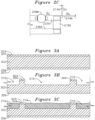
- FIG. 1 shows an example catalytic pre-preg for use in one aspect of the current invention.
- the catalytic pre-preg consists of a matrix of pre-impregnated fibers bound in a resin containing catalytic particles.
- Many different materials may be used for the fibers of prepreg, including woven glass-fiber cloth, carbon-fiber, or other fibers, and a variety of different materials may be used for the resin, including epoxy resin, polyimide resin, cyanate ester resin, PTFE (Teflon) blend resin, or other resins.
- One aspect of the invention is a printed circuit board laminate capable of supporting fine pitch conductive traces on the order of 1 mil (25u), and while the description is drawn to the formation of copper traces using catalysts for electroless copper formation, it is understood that the scope of the invention may be extended to other metals suitable for electroless plating and electro-plating.
- elemental palladium is preferred as the catalyst, although selected periodic table transition metal elements, such as group 9 to 11 platinum (Pt), rhodium (Rh), iridium (Ir), nickel (Ni), gold (Au), silver (Ag), cobalt (Co), or copper (Cu), or other compounds of these, including other metals such as iron (Fe), manganese (Mn), chromium (Cr), molybdenum (Mo), tungsten (W), titanium (Ti), tin (Sn), or mixtures or salts of the above, any of which may be used as catalytic particles.
- periodic table transition metal elements such as group 9 to 11 platinum (Pt), rhodium (Rh), iridium (Ir), nickel (Ni), gold (Au), silver (Ag), cobalt (Co), or copper (Cu), or other compounds of these, including other metals such as iron (Fe), manganese (Mn), chromium (Cr), molybdenum (M
- the present candidate list is intended to be exemplar rather than comprehensive, it is known in the art that other catalysts for attracting copper ions may also be used.
- the catalytic particles are homogeneous catalytic particles.
- the catalytic particles are inorganic particles or high temperature resistant plastic particles which are coated with a few angstrom thickness of catalytic metal, thereby forming heterogeneous catalytic particles having a thin catalytic outer surface encapsulating a non-catalytic inner particle. This formulation may be desirable for larger catalytic particles, such as those on the order of 25u in longest dimension.
- the heterogeneous catalytic particle of this formulation can comprise an inorganic, organic, or inert filler such as silicon dioxide (SiO2), an inorganic clay such as Kaolin, or a high temperature plastic filler coated on the surface with a catalyst such as palladium adsorbed onto the surface of the filler, such as by vapor deposition or chemical deposition. Only a few atomic layers of catalyst are required for the catalytic particle to have desirable properties conducive to electroless plating.
- the catalytic adhesive formulation is the same as for the catalytic laminate except that no fiber is introduced into the resin and catalytic particle mixture and the resin and catalytic particle mixture is applied to an underlying surface and cured such that catalytic particles are an exclusion depth below the surface of the cured catalytic adhesive, as was the case with the catalytic particle distribution of the catalytic laminate layer, thereby enabling electroless plating only in channels which are formed which extend below the exclusion depth for catalytic particles.
- a bath of fillers (organic or inorganic) is sorted by size to include particles less than 25u in size, these sorted inorganic particles are mixed into an aqueous bath in a tank, agitated, and then a palladium salt such as PdCl (or any other catalyst such as a salt of silver of other catalyst) is introduced with an acid such as HCl, and with a reducing agent such as hydrazine hydrate, the mixture thereby reducing metallic Pd which coats the inorganic particles provide a few angstroms of thickness of Pd coated on the filler, thereby creating a heterogeneous catalytic particle which has the catalytic property of a homogeneous Pd particle with a greatly reduced volume requirement of Pd compared to using homogeneous Pd metallic particles.
- homogeneous catalytic particles such as pure Pd may be preferred.
- Example inorganic fillers include clay minerals such as hydrous aluminum phyllosilicates, which may contain variable amounts of iron, magnesium, alkali metals, alkaline earths, and other cations.
- This family of example inorganic fillers includes silicon dioxide, aluminum silicate, kaolinite (Al 2 Si 2 O 5 (OH) 4 ), polysilicate, or other clay minerals which belong to the kaolin or china clay family.
- Example organic fillers include PTFE (Teflon) and other polymers with high temperature resistance.
- the catalytic powder of the present invention may also contain a mixture of heterogeneous catalytic particles (for example, catalytic materials coated over inorganic filler particles), homogeneous catalytic particles (such as elemental palladium), as well as non-catalytic particles (selected from the family of inorganic fillers).
- heterogeneous catalytic particles for example, catalytic materials coated over inorganic filler particles
- homogeneous catalytic particles such as elemental palladium
- non-catalytic particles selected from the family of inorganic fillers.
- a woven glass fiber is fed through as set of rollers infuse the fabric with epoxy resin blended with catalytic particles and mixed with a volatile liquid to reduce the viscosity, thereby forming an A-stage (liquid) pre-preg.
- the resin may be a polyimide resin, a blend of epoxy and cyanide ester (which provides curing at elevated temperatures), or any other suitable resin formulation with selectable viscosity during coating and thermosetting properties after cooling.
- Fire retardants may be added, for example to comply with a flammability standard, or to be compatible with one of the standard FR series of prepreg such as FR-4 or FR-10.
- dielectric constant ⁇ permittivity
- loss tangent ⁇ which is measure of frequency-dependent energy absorption over a distance
- the resin is blended with catalytic particles which have been sorted for size.
- the catalytic particles include at least one of: homogeneous catalytic particles (metallic palladium), or heterogeneous catalytic particles (palladium coated over an inorganic particle or high temperature plastic), and for either formulation, the catalytic particles preferably having a maximum extent of less than 25u and with 50% of the particles by count sized between 12u and 25u, or the range 1-25u, or smaller.
- the catalytic particles are in the size range 1u-25u.
- homogeneous catalytic particles are formed by grinding metallic palladium into particles and passing the resultant particles through a sieve with a mesh having 25u rectangular openings.
- the catalytic resin mixture is formed by blending homogeneous or heterogeneous catalytic particles into the pre-preg resin by a ratio of weights, such as the ratio of substantially 12% catalytic particles by weight to the weight of resin.
- the ratio by weight of catalytic particles in the resin mixture may alternatively be in the range of 8-16% of catalytic particle weight to the total weight of resin. It is understood that other blending ratios may also be used, and it may be preferable to use smaller particles.
- the catalytic particle density is chosen to provide a mean distance between catalytic particles on the order of 3u-5u.
- the pre-preg sheets positioned near the outer surfaces are selected to have greater than 65% resin, such as Glass 106 (71% resin), Glass 1067, or Glass 1035 (65% resin), and the inner prepreg sheets (which are not subject to surface removal) are selected to have less than 65% resin.
- a woven fiberglass may be used with the inner pre-preg layers and a flat unwoven fiberglass may be used in the outer resin rich pre-preg layers.
- the combination of resin-rich pre-preg and flat unwoven fiberglass on the outer surface layer results in an exclusion zone of .7 mil (17u) to .9 mil (23u) between an outer surface and the encapsulated fiberglass.
- Glass styles 106, 1035, and 1067 are preferred for use on the outer resin rich surface since the glass fiber thicknesses are smaller (1.3-1.4 mil / 33-35u) than the glass fiber thickness found in typical pre-preg sheets with greater than 65% resin used in the central regions of the laminate, such as glass style 2116, which has 3.7 mil (94u) fibers. These values are given as examples, the smallest glass fibers which are commercially available are expected to continue to reduce in diameter.
- a temperature vs. time sequence is applied to cause the catalytic particles and fiberglass to migrate away from the outer surface of the laminate, repelled by the surface tension of the epoxy during a liquid state of the gel point temperature.
- the cured C-stage pre-preg sheets are offloaded.
- the process which forms the cured C-stage pre-preg sheets may use single or multiple sheets of fiber fabric to vary the finished thickness, which may vary from 2 mil (51u) to 60 mil (1.5mm).
- Prior art catalytic laminates have activated surfaces that must be masked to prevent unwanted electroless plating on the activated surface of the catalytic laminate.
- the catalytic laminate and catalytic adhesives of the present invention exclude catalytic particles over the thickness extent from first surface 104 to first boundary 108, and from second surface 106 to second boundary 110, providing the benefit that a separate mask layer preventing contact with the catalytic particles is not required for electroless plating as it is in the prior art. Accordingly, removal of surface material from either first surface 104 to the depth of boundary layer 108 or deeper, or removal of surface material from second surface 106 to second boundary 110, results in the exposure of catalytic material which may be used for electroless plating.
- Figure 2A shows a prior art buck regulator circuit.
- switch 202 When the switch 202 is closed, inductor charging current flows from the power source 204 through energy storage inductor 208 and to smoothing capacitor 218, increasing the voltage in smoothing capacitor 218.
- switch 202 When switch 202 is open, inductor discharge current continues to flow through inductor 208, through the path of diode 212 and capacitor 218.
- Steady state currents I3 and I4 drawn by load 214 and 216, respectively, are significantly lower than the peak pulsatile current I1 206 through switch 202 or peak pulsatile current I2 210 through inductor 208.
- Figure 2C illustrates an example of the effect on a prior art printed circuit board which is designed for pulsatile vs steady state current flows.
- Inductor 208A corresponds to 208 of figure 2A and capacitor 218A of figure 2C corresponds to 218 of figure 2A .
- the trace 237A (corresponding to thick line 237 of schematic of figure 2A ) carries peak pulsatile currents and so must be comparatively wide to reduce I 2 R losses associated with I2, whereas the width of the traces 214A and 216A carrying steady state currents I3 and I4 (associated with corresponding lines 214 and 216 of figure 2A ) may be significantly narrower.
- traces which can grow in thickness rather than width, and which can utilize the thickness of two or more layers of a multi-layer circuit board to form the conductive traces.
- FIG. 3A shows a cross section view of a catalytic laminate (or catalytic adhesive) 302 with the catalytic particle distribution plot of figure 1 , where the catalytic particles are distributed throughout the inner regions of the catalytic layer (either a catalytic laminate or catalytic adhesive), and the catalytic particles are below the surface exclusion depth 306 and 304 of the associated outer surfaces, thereby providing a density of catalytic particles from 304 to 306 which is sufficient to provide electroless deposition of conductive metal such as copper in regions which extend below the surface catalytic particle exclusion zone, and to exclude electroless deposition at native surfaces 303 or 307.
- conductive metal such as copper
- Catalytic particles (not shown) in the region between 304 and 306 may be in the size range of 25u and smaller, in the present example they may be in the range 12u to 25u.
- the catalytic particles may include heterogeneous catalytic particles (organic or inorganic particles having a catalytic surface coating) or homogeneous particles (catalytic metal particles), as described previously.
- the exclusion boundary 304 is approximately 25u below the first surface 303.
- the second surface 307 and second surface exclusion boundary 306 on the opposite surface are shown for reference, but it is understood that the process may be used on one or both sides of a candidate catalytic laminate or catalytic adhesive.
- Figure 3B shows the laminate of figure 3A with a channel 310 formed by removal of the surface layer 303 below exclusion zone 304 in a region where a trace is desired.
- the removal of surface material to form channels in the catalytic laminate or catalytic adhesive 302 may be by laser ablation, where the temperature of the catalytic pre-preg is instantly elevated until the catalytic pre-preg is vaporized, while leaving the surrounding catalytic prepreg structurally unchanged, leaving the catalytic particles exposed. It may be preferable to use a laser with a wavelength with a low reflectivity and high absorption of this optical wavelength for the pre-preg material being ablated, such as ultraviolet (UV) wavelengths.
- UV ultraviolet
- UV lasers examples include the UV excimer laser or yttrium-aluminum-garnet (YAG) laser, which are also good choices because of the narrow beam extent and high available power which for forming channels of precise mechanical depth and with well-defined sidewalls.
- An example laser may remove material in a 0.9-1.1 mil (23u to 28u) diameter width with a depth governed by laser power and speed of movement across the surface.
- Another surface removal technique for forming channel 210 is plasma etching, which may be done locally or by preparing the surface with a patterned mask which excludes the plasma from the surface layers 206 or 205, such as a dry film photoresist or other mask material which has a low plasma etch rate compared to the plasma etch rate of catalytic pre-preg.
- the photoresist thickness is typically chosen based on epoxy/photoresist etch selectivity (such that plasma etch to the desired depth of removal of the cured epoxy leaves sufficient photoresist at the end of the etch), or in the case of photoresist which is used as an electroplate mask, the thickness is chosen according to desired deposition thickness. Typical dry film thickness is in the range of 0.8-2.5 mil (20-64u).
- Plasmas suitable for etching the resin rich surface include mixtures of oxygen (O) and CF 4 plasmas, mixed with inert gasses such as nitrogen (N), or argon (Ar) may be added as carrier gasses for the reactive gases.
- a mask pattern may also be formed with a dry film mask, metal mask, or any other type of mask having apertures.
- the etch resist may be applied using any of photolithography, screen printing, stenciling, squeegee, or any method of application of etch resist.
- Another method for removal of the surface layer of catalytic pre-preg is mechanical grinding, such as a linear or rotational cutting tool.
- the catalytic pre-preg may be secured in a vacuum plate chuck, and a rotating cutter (or fixed cutter with movable vacuum plate) may travel a pattern defining the traces such as defined by x,y coordinate pairs of a Gerber format photofile.
- a water cutting tool may be used, where a water jet with abrasive particles entrained in the stream may impinge on the surface, thereby removing material below the first boundary 304. Any of these methods may be used separately or in combination to remove surface material and form channel 310 from catalytic pre-preg 302, with the channel extending below the first boundary 304.
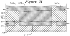
- Figure 3E shows the removal of catalytic layer 326 through the depth of catalytic layer 320 using the previously described method from the surface 321 of catalytic layer 320 through to the underlying electroless deposition 314 of the first layer 302.
- the formation of the channel 326 may be done using any known method for removing laminate, although laser ablation is preferred.
- Figure 3F shows electroless plating 329 of the channel 326 from the deposition 314 below to the top level 321 of the catalytic layer 320.
- the resulting circuit board now has a homogeneous trace with a trace thickness which is greater than the thickness of a single catalytic layer 320 or 302.
- the circuit board may be used in a finished form of figure 3F in this manner after the addition of components.
- High current trace segments such as trace segment 320 of figure 2C , may have its resistance reduced using the current method, and additional layers may be bonded or laminated to continue the process and increase the depth of the trace segment, as shown in figure 3G where catalytic layer 332 (where first exclusion surface 330 and second exclusion surface 334 may be present, as before).
- Figure 3H shows the subsequent step of forming channel 336 in catalytic layer 332 of figure 3G .
- Figure 3I shows a final step, where electroless deposition of metal 340 is in electrical contact with previous electroless depositions 329 and 314, thereby providing a method for forming a low resistance elongate conductor of selectable thickness, which can be narrower than allowed by the prior art for a given deposition metal resistivity (which translates to resistance per inch for a given trace thickness and width) of trace having a greater depth than provided in the prior art.
- the electroless metal deposition is homogeneous across layers, providing a low resistance trace which spans the several dielectric layers and without the boundaries shown in the figures.
- Electroless plating for 329 of figure 3F and 314 of figure 3C may be performed several different ways.
- One example electroless copper bath formulation uses a mixture of Rochelle salt as the complexing agent, copper sulfate as the copper metal source, formaldehyde as the reducing agent, and sodium hydroxide as a reactant.
- the tartrate (Rochelle salt) bath is preferred for ease of waste treatment; the Rochelle salt does not chelate as strongly as alternatives such as EDTA or quadrol.
- the tartrate (Rochelle salt) is the completing agent, copper sulfate is the metal source, formaldehyde is the reducing agent, and sodium hydroxide is a reactant.
- Other electroless plating formulations are possible, this example is given for reference. The electroless plating initially forms over the surfaces of the exposed catalytic particles and progresses until the deposition is below the native outer surfaces of the catalytic layer.
- a key advantage of electroless plating of channels etched in catalytic material is that the electroless plating progresses on all three sides at once, compared to electroplating which only progresses from a bottom (initially plated) layer.
- Figure 4 shows a series of process steps for using catalytic layers (catalytic adhesive or catalytic laminate) to form circuit boards with trace layers having a thickness greater than a single laminate layer thickness.
- Apertures are formed in step 402 such as for interlayer vias (not shown but well known in the prior art), followed by channels in step 404 such as channel 310 of figure 3B .
- Electroless plating is performed in step 406 corresponding to 314 of figure 3C , and a series of steps 408, 410, and 412 are iteratively performed as needed for each layer of laminate/channel/electroless plate to extend the thickness of the electroless deposition of step 406.
- Step 408 corresponds to the bonded or laminated subsequent layers 320 of step 3D and layer 332 to 302 of step 3G.
- Step 410 corresponds to the formation of channels 326 of figure 3E or 336 of figure 3H .
- Step 412 corresponds to the electroless plating 329 of figure 3F or 340 of figure 3I .
- the process of adding additional layers to further extend the thickness of the traces may be performed by the path 414 following step 412 for each iteration.
- trace structures of figures 3A to 3I are shown in combination as they would normally occur on a PCB, these examples are only for illustration, and are not intended to limit the invention to these constructions.
- the result of using the present invention for the example given in figure 2A and 2C is that if trace 237A is .25" wide and 3 mil thick for a conventional subtractive circuit board process, and the top and underlying catalytic layers 15 mil thick (30 mil total) were used to form the trace described in figures 3A to 3I , then trace 237 could be reduced from 250 mil to 25 mil width.
- Certain post-processing operations are not shown which are generic to printed circuit board manufacturing and may be performed using prior art methods on boards produced according to the novel process. Such operations include tin plating for improved solder flow, gold flash for improved conductivity and reduced corrosion, soldermask operations, silkscreening information on the board (part number, reference designators, etc.), scoring the finished board or providing breakaway tabs, etc.
- the circuit board formed using the current process has a planar surface compared to the prior art of subtractive copper etching which leaves an elevated trace on top of a lower underlying substrate. Certain of these operations may produce improved results when performed on the co-planar trace and substrate surfaces of the present invention. For example, silkscreened lettering over traces or vias traditionally breaks up because of trace and via thickness over the board surface, whereas these operations would provide superior results on a planarized surface.
Landscapes
- Engineering & Computer Science (AREA)
- Chemical & Material Sciences (AREA)
- Microelectronics & Electronic Packaging (AREA)
- Manufacturing & Machinery (AREA)
- Materials Engineering (AREA)
- Mechanical Engineering (AREA)
- Metallurgy (AREA)
- Organic Chemistry (AREA)
- Chemical Kinetics & Catalysis (AREA)
- General Chemical & Material Sciences (AREA)
- Inorganic Chemistry (AREA)
- Manufacturing Of Printed Wiring (AREA)
- Chemically Coating (AREA)
- Production Of Multi-Layered Print Wiring Board (AREA)
- Printing Elements For Providing Electric Connections Between Printed Circuits (AREA)
Claims (11)
- Mehrschichtige Leiterplatte, umfassendeine erste Katalyseschicht mit einer Oberfläche, die eine unzureichende Dichte von Katalysepartikeln aufweist, um eine stromlose Beschichtung zu ermöglichen, es sei denn ein Kanal, der sich bis in die untere Ausgrenzung erstreckt, ist erreicht, wobei die erste Katalyseschicht eine Leiterbahn aufweist, die durch außenstromlose Abscheidung in einem Kanal in der ersten Katalyseschicht ausgebildet wird, wobei der Kanal in die erste Katalyseschicht und unter der untere Ausgrenzung für Katalysepartikel verläuft;eine zweite Katalyseschicht, die auf die erste Katalyseschicht aufgebracht, geklebt oder beschichtet wird, wobei die zweite Katalyseschicht einen Kanal aufweist, der durch die Dicke der zweiten Katalyseschicht ausgebildet wird und in die Tiefe zur Leiterbahn der ersten Katalyseschicht verläuft;wobei der Kanal der zweiten Katalyseschicht mit einem leitenden Metall durch außenstromlose Abscheidung gefüllt ist und in Kontakt mit der außenstromlose Abscheidung der ersten Katalyseschicht ist.
- Mehrschichtige Leiterplatte nach Anspruch 1, wobei die erste Katalyseschicht oder die zweite Katalyseschicht unter Verwendung heterogener Katalysepartikel ausgebildet wird.
- Mehrschichtige Leiterplatte nach Anspruch 2, wobei die heterogenen Katalysepartikel ein anorganisches Material umfassen, das mit einem Katalysator überzogen ist.
- Mehrschichtige Leiterplatte nach Anspruch 3, wobei der Katalysator der heterogenen Katalysepartikel mindestens eins von Folgendem umfasst: Palladium (Pd), Rhodium (Rh), Iridium (Ir), Nickel (Ni), Gold (Au), Silber (Ag), Cobalt (Co), oder Kupfer (Cu), oder Verbindungen daraus, die andere Metalle umfassen können, etwa Eisen (Fe), Mangan (Mn), Chrom (Cr), Molybdän (Mo), Wolfram (W), Titan (Ti), Zinn (Sn) oder Mischungen oder Salze davon.
- Mehrschichtige Leiterplatte nach Anspruch 3, wobei der Katalysator der heterogenen Katalysepartikel Palladium-Salz enthält, die mindestens eins von Folgendem umfassen: BrPd, CL2Pd, Pd(CN)2, I2Pd, Pd(NO3)2*2H2O, Pd(NO3)2, PdSO4, Pd(NH3)4Br2, Pd(NH3)4Cl2H2O.
- Mehrschichtige Leiterplatte nach Anspruch 1, wobei die erste Katalyseschicht oder die zweite Katalyseschicht ein Harz umfasst, das mindestens eins von Folgendem umfasst: Polyimidharz oder Mischung aus Epoxid und Cyanatester.
- Mehrschichtige Leiterplatte nach Anspruch 1, wobei mindestens eine der ersten Katalyseschicht oder der zweiten Katalyseschicht ein Katalyseklebstoff oder Katalyseschichtstoff ist.
- Mehrschichtige Leiterplatte nach einem der Ansprüche 2 bis 5, wobei die Mehrheit der heterogenen Katalysepartikel im längsten Maß kleiner als 25 u ist.
- Mehrschichtige Leiterplatte nach Anspruch 2, wobei die heterogenen Katalysepartikel einen anorganischen Füllstoff umfassen, der mit einem Katalysator überzogen ist, und der Füllstoff mindestens eins von einem anorganischen Füllstoff, inerten Füllstoff, Tonfüllstoff wie Kaolin oder einem Hochtemperatur-Kunststofffüllstoff umfasst.
- Mehrschichtige Leiterplatte nach Anspruch 1, wobei mindestens eins von der ersten Katalyseschicht oder der zweiten Katalyseschicht eine Matrix aus vorab imprägnierten Fasern umfasst, die in einem Harz gebunden sind, das Katalysepartikel enthält.
- Mehrschichtige Leiterplatte nach Anspruch 10, wobei die Fasern ein Fasergeflecht umfassen.
Applications Claiming Priority (2)
| Application Number | Priority Date | Filing Date | Title |
|---|---|---|---|
| US16/237,702 US11039540B2 (en) | 2019-01-01 | 2019-01-01 | Multi-layer circuit board with traces thicker than a circuit board layer |
| PCT/US2019/066990 WO2020142209A1 (en) | 2019-01-01 | 2019-12-17 | Multi-layer circuit board with traces thicker than a circuit board layer |
Publications (4)
| Publication Number | Publication Date |
|---|---|
| EP3906329A1 EP3906329A1 (de) | 2021-11-10 |
| EP3906329A4 EP3906329A4 (de) | 2022-10-05 |
| EP3906329C0 EP3906329C0 (de) | 2025-02-05 |
| EP3906329B1 true EP3906329B1 (de) | 2025-02-05 |
Family
ID=71124513
Family Applications (1)
| Application Number | Title | Priority Date | Filing Date |
|---|---|---|---|
| EP19907701.7A Active EP3906329B1 (de) | 2019-01-01 | 2019-12-17 | Mehrschichtige leiterplatte mit leiterbahnen, die dicker als eine leiterplattenschicht sind |
Country Status (6)
| Country | Link |
|---|---|
| US (2) | US11039540B2 (de) |
| EP (1) | EP3906329B1 (de) |
| JP (2) | JP7676309B2 (de) |
| KR (1) | KR102803528B1 (de) |
| CN (1) | CN113544311B (de) |
| WO (1) | WO2020142209A1 (de) |
Families Citing this family (2)
| Publication number | Priority date | Publication date | Assignee | Title |
|---|---|---|---|---|
| WO2023043196A1 (ko) | 2021-09-14 | 2023-03-23 | 주식회사 엘지에너지솔루션 | 전극조립체, 이를 포함하는 이차전지, 이를 제조하는 이차전지 제조방법 및 이에 이용되는 이차전지 제조장치 |
| CN114980566B (zh) * | 2022-07-27 | 2022-10-28 | 四川英创力电子科技股份有限公司 | 一种阶梯线路制作方法 |
Family Cites Families (20)
| Publication number | Priority date | Publication date | Assignee | Title |
|---|---|---|---|---|
| JPH0936522A (ja) * | 1995-07-14 | 1997-02-07 | Fuji Kiko Denshi Kk | プリント配線板における回路形成方法 |
| KR100906931B1 (ko) * | 1998-02-26 | 2009-07-10 | 이비덴 가부시키가이샤 | 필드 바이어 구조를 갖는 다층프린트 배선판 |
| TW512653B (en) * | 1999-11-26 | 2002-12-01 | Ibiden Co Ltd | Multilayer circuit board and semiconductor device |
| JP2001291721A (ja) * | 2000-04-06 | 2001-10-19 | Nec Corp | 配線構造、導電パターンの形成方法、半導体装置および半導体装置の製造方法 |
| US10198908B2 (en) * | 2002-09-30 | 2019-02-05 | Stanley P. Dabrowski | Method and apparatus for integrated customer tracking and browsing |
| US20050233555A1 (en) * | 2004-04-19 | 2005-10-20 | Nagarajan Rajagopalan | Adhesion improvement for low k dielectrics to conductive materials |
| US20060113675A1 (en) * | 2004-12-01 | 2006-06-01 | Chung-Liang Chang | Barrier material and process for Cu interconnect |
| US8240036B2 (en) * | 2008-04-30 | 2012-08-14 | Panasonic Corporation | Method of producing a circuit board |
| EP2469990B1 (de) * | 2008-04-30 | 2014-01-15 | Panasonic Corporation | Verfahren zur Herstellung einer Leiterplatte mittels Additivverfahren. |
| CN103929903A (zh) * | 2013-01-15 | 2014-07-16 | 日本特殊陶业株式会社 | 布线基板的制造方法 |
| US8916469B2 (en) * | 2013-03-12 | 2014-12-23 | Taiwan Semiconductor Manufacturing Company, Ltd. | Method of fabricating copper damascene |
| US9380700B2 (en) * | 2014-05-19 | 2016-06-28 | Sierra Circuits, Inc. | Method for forming traces of a printed circuit board |
| US9398703B2 (en) | 2014-05-19 | 2016-07-19 | Sierra Circuits, Inc. | Via in a printed circuit board |
| US9631279B2 (en) | 2014-05-19 | 2017-04-25 | Sierra Circuits, Inc. | Methods for forming embedded traces |
| US20160278206A1 (en) * | 2014-05-19 | 2016-09-22 | Sierra Circuits, Inc. | Printed circuit board |
| US9405419B2 (en) * | 2014-11-11 | 2016-08-02 | Eastman Kodak Company | Electrically-conductive articles with electrically-conductive metallic connectors |
| US20160240419A1 (en) * | 2015-02-13 | 2016-08-18 | Eastman Kodak Company | Atomic-layer deposition substrate |
| US9706650B1 (en) * | 2016-08-18 | 2017-07-11 | Sierra Circuits, Inc. | Catalytic laminate apparatus and method |
| US9922951B1 (en) * | 2016-11-12 | 2018-03-20 | Sierra Circuits, Inc. | Integrated circuit wafer integration with catalytic laminate or adhesive |
| US10765012B2 (en) * | 2017-07-10 | 2020-09-01 | Catlam, Llc | Process for printed circuit boards using backing foil |
-
2019
- 2019-01-01 US US16/237,702 patent/US11039540B2/en active Active
- 2019-12-17 JP JP2021538684A patent/JP7676309B2/ja active Active
- 2019-12-17 CN CN201980093241.6A patent/CN113544311B/zh active Active
- 2019-12-17 EP EP19907701.7A patent/EP3906329B1/de active Active
- 2019-12-17 WO PCT/US2019/066990 patent/WO2020142209A1/en not_active Ceased
- 2019-12-17 KR KR1020217024423A patent/KR102803528B1/ko active Active
-
2021
- 2021-05-11 US US17/317,203 patent/US11406024B2/en active Active
-
2024
- 2024-10-03 JP JP2024174325A patent/JP2024177400A/ja active Pending
Also Published As
| Publication number | Publication date |
|---|---|
| KR102803528B1 (ko) | 2025-05-02 |
| EP3906329C0 (de) | 2025-02-05 |
| JP2022516625A (ja) | 2022-03-01 |
| US20210282274A1 (en) | 2021-09-09 |
| JP2024177400A (ja) | 2024-12-19 |
| EP3906329A1 (de) | 2021-11-10 |
| US20200214144A1 (en) | 2020-07-02 |
| CN113544311A (zh) | 2021-10-22 |
| JP7676309B2 (ja) | 2025-05-14 |
| US11039540B2 (en) | 2021-06-15 |
| EP3906329A4 (de) | 2022-10-05 |
| US11406024B2 (en) | 2022-08-02 |
| CN113544311B (zh) | 2022-08-26 |
| WO2020142209A1 (en) | 2020-07-09 |
| KR20210122787A (ko) | 2021-10-12 |
Similar Documents
| Publication | Publication Date | Title |
|---|---|---|
| US12513827B2 (en) | Semi-additive process for catalytic printed circuit boards | |
| US10765003B2 (en) | Method for making a multi-layer circuit board using conductive paste with interposer layer | |
| US10959329B2 (en) | Circuit board using non-catalytic laminate with catalytic adhesive overlay | |
| US11653453B2 (en) | Electroless and electrolytic deposition process for forming traces on a catalytic laminate | |
| JP2024177400A (ja) | 回路板層より厚いトレースを有する多層回路板 | |
| KR102649271B1 (ko) | 트레이스 및 비아를 갖는 플라스마 에칭 촉매 라미네이트 | |
| US20200008306A1 (en) | UV curable Catalytic Adhesive for Circuit Boards with Traces and Vias | |
| US20230096301A1 (en) | Circuit Board Traces in Channels using Electroless and Electroplated Depositions |
Legal Events
| Date | Code | Title | Description |
|---|---|---|---|
| STAA | Information on the status of an ep patent application or granted ep patent |
Free format text: STATUS: THE INTERNATIONAL PUBLICATION HAS BEEN MADE |
|
| PUAI | Public reference made under article 153(3) epc to a published international application that has entered the european phase |
Free format text: ORIGINAL CODE: 0009012 |
|
| STAA | Information on the status of an ep patent application or granted ep patent |
Free format text: STATUS: REQUEST FOR EXAMINATION WAS MADE |
|
| 17P | Request for examination filed |
Effective date: 20210802 |
|
| AK | Designated contracting states |
Kind code of ref document: A1 Designated state(s): AL AT BE BG CH CY CZ DE DK EE ES FI FR GB GR HR HU IE IS IT LI LT LU LV MC MK MT NL NO PL PT RO RS SE SI SK SM TR |
|
| DAV | Request for validation of the european patent (deleted) | ||
| DAX | Request for extension of the european patent (deleted) | ||
| A4 | Supplementary search report drawn up and despatched |
Effective date: 20220901 |
|
| RIC1 | Information provided on ipc code assigned before grant |
Ipc: H05K 3/46 20060101ALI20220826BHEP Ipc: H05K 3/18 20060101ALI20220826BHEP Ipc: H05K 3/10 20060101ALI20220826BHEP Ipc: H05K 1/11 20060101ALI20220826BHEP Ipc: H05K 1/09 20060101ALI20220826BHEP Ipc: H05K 1/03 20060101ALI20220826BHEP Ipc: H05K 1/02 20060101ALI20220826BHEP Ipc: C23C 18/38 20060101ALI20220826BHEP Ipc: C23C 18/16 20060101AFI20220826BHEP |
|
| RIN1 | Information on inventor provided before grant (corrected) |
Inventor name: BAHL, KENNETH S. |
|
| GRAP | Despatch of communication of intention to grant a patent |
Free format text: ORIGINAL CODE: EPIDOSNIGR1 |
|
| STAA | Information on the status of an ep patent application or granted ep patent |
Free format text: STATUS: GRANT OF PATENT IS INTENDED |
|
| INTG | Intention to grant announced |
Effective date: 20240924 |
|
| GRAS | Grant fee paid |
Free format text: ORIGINAL CODE: EPIDOSNIGR3 |
|
| GRAA | (expected) grant |
Free format text: ORIGINAL CODE: 0009210 |
|
| STAA | Information on the status of an ep patent application or granted ep patent |
Free format text: STATUS: THE PATENT HAS BEEN GRANTED |
|
| AK | Designated contracting states |
Kind code of ref document: B1 Designated state(s): AL AT BE BG CH CY CZ DE DK EE ES FI FR GB GR HR HU IE IS IT LI LT LU LV MC MK MT NL NO PL PT RO RS SE SI SK SM TR |
|
| REG | Reference to a national code |
Ref country code: GB Ref legal event code: FG4D |
|
| REG | Reference to a national code |
Ref country code: CH Ref legal event code: EP |
|
| REG | Reference to a national code |
Ref country code: IE Ref legal event code: FG4D |
|
| REG | Reference to a national code |
Ref country code: DE Ref legal event code: R096 Ref document number: 602019065668 Country of ref document: DE |
|
| U01 | Request for unitary effect filed |
Effective date: 20250205 |
|
| U07 | Unitary effect registered |
Designated state(s): AT BE BG DE DK EE FI FR IT LT LU LV MT NL PT RO SE SI Effective date: 20250211 |
|
| PG25 | Lapsed in a contracting state [announced via postgrant information from national office to epo] |
Ref country code: RS Free format text: LAPSE BECAUSE OF FAILURE TO SUBMIT A TRANSLATION OF THE DESCRIPTION OR TO PAY THE FEE WITHIN THE PRESCRIBED TIME-LIMIT Effective date: 20250505 |
|
| PG25 | Lapsed in a contracting state [announced via postgrant information from national office to epo] |
Ref country code: PL Free format text: LAPSE BECAUSE OF FAILURE TO SUBMIT A TRANSLATION OF THE DESCRIPTION OR TO PAY THE FEE WITHIN THE PRESCRIBED TIME-LIMIT Effective date: 20250205 |
|
| PG25 | Lapsed in a contracting state [announced via postgrant information from national office to epo] |
Ref country code: ES Free format text: LAPSE BECAUSE OF FAILURE TO SUBMIT A TRANSLATION OF THE DESCRIPTION OR TO PAY THE FEE WITHIN THE PRESCRIBED TIME-LIMIT Effective date: 20250205 |
|
| PG25 | Lapsed in a contracting state [announced via postgrant information from national office to epo] |
Ref country code: IS Free format text: LAPSE BECAUSE OF FAILURE TO SUBMIT A TRANSLATION OF THE DESCRIPTION OR TO PAY THE FEE WITHIN THE PRESCRIBED TIME-LIMIT Effective date: 20250605 Ref country code: NO Free format text: LAPSE BECAUSE OF FAILURE TO SUBMIT A TRANSLATION OF THE DESCRIPTION OR TO PAY THE FEE WITHIN THE PRESCRIBED TIME-LIMIT Effective date: 20250505 |
|
| PG25 | Lapsed in a contracting state [announced via postgrant information from national office to epo] |
Ref country code: HR Free format text: LAPSE BECAUSE OF FAILURE TO SUBMIT A TRANSLATION OF THE DESCRIPTION OR TO PAY THE FEE WITHIN THE PRESCRIBED TIME-LIMIT Effective date: 20250205 |
|
| PG25 | Lapsed in a contracting state [announced via postgrant information from national office to epo] |
Ref country code: GR Free format text: LAPSE BECAUSE OF FAILURE TO SUBMIT A TRANSLATION OF THE DESCRIPTION OR TO PAY THE FEE WITHIN THE PRESCRIBED TIME-LIMIT Effective date: 20250506 |
|
| PG25 | Lapsed in a contracting state [announced via postgrant information from national office to epo] |
Ref country code: SM Free format text: LAPSE BECAUSE OF FAILURE TO SUBMIT A TRANSLATION OF THE DESCRIPTION OR TO PAY THE FEE WITHIN THE PRESCRIBED TIME-LIMIT Effective date: 20250205 |
|
| PG25 | Lapsed in a contracting state [announced via postgrant information from national office to epo] |
Ref country code: CZ Free format text: LAPSE BECAUSE OF FAILURE TO SUBMIT A TRANSLATION OF THE DESCRIPTION OR TO PAY THE FEE WITHIN THE PRESCRIBED TIME-LIMIT Effective date: 20250205 |
|
| PG25 | Lapsed in a contracting state [announced via postgrant information from national office to epo] |
Ref country code: SK Free format text: LAPSE BECAUSE OF FAILURE TO SUBMIT A TRANSLATION OF THE DESCRIPTION OR TO PAY THE FEE WITHIN THE PRESCRIBED TIME-LIMIT Effective date: 20250205 |
|
| PLBE | No opposition filed within time limit |
Free format text: ORIGINAL CODE: 0009261 |
|
| STAA | Information on the status of an ep patent application or granted ep patent |
Free format text: STATUS: NO OPPOSITION FILED WITHIN TIME LIMIT |
|
| REG | Reference to a national code |
Ref country code: CH Ref legal event code: L10 Free format text: ST27 STATUS EVENT CODE: U-0-0-L10-L00 (AS PROVIDED BY THE NATIONAL OFFICE) Effective date: 20251217 |
|
| REG | Reference to a national code |
Ref country code: CH Ref legal event code: U11 Free format text: ST27 STATUS EVENT CODE: U-0-0-U10-U11 (AS PROVIDED BY THE NATIONAL OFFICE) Effective date: 20260101 |
|
| PGFP | Annual fee paid to national office [announced via postgrant information from national office to epo] |
Ref country code: GB Payment date: 20251219 Year of fee payment: 7 |
|
| 26N | No opposition filed |
Effective date: 20251106 |
|
| U20 | Renewal fee for the european patent with unitary effect paid |
Year of fee payment: 7 Effective date: 20251230 |